US9812155B1 - Method and system for fabricating high junction angle read sensors - Google Patents
Method and system for fabricating high junction angle read sensors Download PDFInfo
- Publication number
- US9812155B1 US9812155B1 US14/949,155 US201514949155A US9812155B1 US 9812155 B1 US9812155 B1 US 9812155B1 US 201514949155 A US201514949155 A US 201514949155A US 9812155 B1 US9812155 B1 US 9812155B1
- Authority
- US
- United States
- Prior art keywords
- layer
- read
- magnetic
- read sensor
- angle
- Prior art date
- Legal status (The legal status is an assumption and is not a legal conclusion. Google has not performed a legal analysis and makes no representation as to the accuracy of the status listed.)
- Active
Links
- 238000000034 method Methods 0.000 title abstract description 41
- 230000005291 magnetic effect Effects 0.000 claims abstract description 130
- 239000000463 material Substances 0.000 claims abstract description 45
- 230000005415 magnetization Effects 0.000 claims abstract description 19
- 239000010410 layer Substances 0.000 description 141
- 150000002500 ions Chemical class 0.000 description 55
- 230000005290 antiferromagnetic effect Effects 0.000 description 8
- 230000005641 tunneling Effects 0.000 description 8
- 238000013500 data storage Methods 0.000 description 7
- 238000000151 deposition Methods 0.000 description 7
- 230000009977 dual effect Effects 0.000 description 6
- 230000006872 improvement Effects 0.000 description 5
- 238000004519 manufacturing process Methods 0.000 description 5
- 125000006850 spacer group Chemical group 0.000 description 5
- 230000004888 barrier function Effects 0.000 description 4
- 230000015572 biosynthetic process Effects 0.000 description 3
- 238000003801 milling Methods 0.000 description 2
- 239000002356 single layer Substances 0.000 description 2
- 238000003860 storage Methods 0.000 description 2
- 229910003321 CoFe Inorganic materials 0.000 description 1
- 230000002411 adverse Effects 0.000 description 1
- 239000000956 alloy Substances 0.000 description 1
- 229910045601 alloy Inorganic materials 0.000 description 1
- 230000001771 impaired effect Effects 0.000 description 1
- 239000012212 insulator Substances 0.000 description 1
- 239000011159 matrix material Substances 0.000 description 1
- 239000002245 particle Substances 0.000 description 1
- 230000009467 reduction Effects 0.000 description 1
- 238000000992 sputter etching Methods 0.000 description 1
Images


Classifications
-
- G—PHYSICS
- G11—INFORMATION STORAGE
- G11B—INFORMATION STORAGE BASED ON RELATIVE MOVEMENT BETWEEN RECORD CARRIER AND TRANSDUCER
- G11B5/00—Recording by magnetisation or demagnetisation of a record carrier; Reproducing by magnetic means; Record carriers therefor
- G11B5/127—Structure or manufacture of heads, e.g. inductive
- G11B5/1272—Assembling or shaping of elements
-
- G—PHYSICS
- G11—INFORMATION STORAGE
- G11B—INFORMATION STORAGE BASED ON RELATIVE MOVEMENT BETWEEN RECORD CARRIER AND TRANSDUCER
- G11B5/00—Recording by magnetisation or demagnetisation of a record carrier; Reproducing by magnetic means; Record carriers therefor
- G11B5/127—Structure or manufacture of heads, e.g. inductive
- G11B5/31—Structure or manufacture of heads, e.g. inductive using thin films
- G11B5/3163—Fabrication methods or processes specially adapted for a particular head structure, e.g. using base layers for electroplating, using functional layers for masking, using energy or particle beams for shaping the structure or modifying the properties of the basic layers
-
- G—PHYSICS
- G11—INFORMATION STORAGE
- G11B—INFORMATION STORAGE BASED ON RELATIVE MOVEMENT BETWEEN RECORD CARRIER AND TRANSDUCER
- G11B5/00—Recording by magnetisation or demagnetisation of a record carrier; Reproducing by magnetic means; Record carriers therefor
- G11B5/127—Structure or manufacture of heads, e.g. inductive
- G11B5/33—Structure or manufacture of flux-sensitive heads, i.e. for reproduction only; Combination of such heads with means for recording or erasing only
- G11B5/39—Structure or manufacture of flux-sensitive heads, i.e. for reproduction only; Combination of such heads with means for recording or erasing only using magneto-resistive devices or effects
- G11B5/3903—Structure or manufacture of flux-sensitive heads, i.e. for reproduction only; Combination of such heads with means for recording or erasing only using magneto-resistive devices or effects using magnetic thin film layers or their effects, the films being part of integrated structures
- G11B5/3906—Details related to the use of magnetic thin film layers or to their effects
- G11B5/3909—Arrangements using a magnetic tunnel junction
-
- G—PHYSICS
- G11—INFORMATION STORAGE
- G11B—INFORMATION STORAGE BASED ON RELATIVE MOVEMENT BETWEEN RECORD CARRIER AND TRANSDUCER
- G11B5/00—Recording by magnetisation or demagnetisation of a record carrier; Reproducing by magnetic means; Record carriers therefor
- G11B5/127—Structure or manufacture of heads, e.g. inductive
- G11B5/33—Structure or manufacture of flux-sensitive heads, i.e. for reproduction only; Combination of such heads with means for recording or erasing only
- G11B5/39—Structure or manufacture of flux-sensitive heads, i.e. for reproduction only; Combination of such heads with means for recording or erasing only using magneto-resistive devices or effects
- G11B5/3903—Structure or manufacture of flux-sensitive heads, i.e. for reproduction only; Combination of such heads with means for recording or erasing only using magneto-resistive devices or effects using magnetic thin film layers or their effects, the films being part of integrated structures
- G11B5/3906—Details related to the use of magnetic thin film layers or to their effects
- G11B5/3912—Arrangements in which the active read-out elements are transducing in association with active magnetic shields, e.g. magnetically coupled shields
-
- G—PHYSICS
- G11—INFORMATION STORAGE
- G11B—INFORMATION STORAGE BASED ON RELATIVE MOVEMENT BETWEEN RECORD CARRIER AND TRANSDUCER
- G11B5/00—Recording by magnetisation or demagnetisation of a record carrier; Reproducing by magnetic means; Record carriers therefor
- G11B5/127—Structure or manufacture of heads, e.g. inductive
- G11B5/33—Structure or manufacture of flux-sensitive heads, i.e. for reproduction only; Combination of such heads with means for recording or erasing only
- G11B5/39—Structure or manufacture of flux-sensitive heads, i.e. for reproduction only; Combination of such heads with means for recording or erasing only using magneto-resistive devices or effects
- G11B5/3903—Structure or manufacture of flux-sensitive heads, i.e. for reproduction only; Combination of such heads with means for recording or erasing only using magneto-resistive devices or effects using magnetic thin film layers or their effects, the films being part of integrated structures
- G11B5/3906—Details related to the use of magnetic thin film layers or to their effects
- G11B5/3929—Disposition of magnetic thin films not used for directly coupling magnetic flux from the track to the MR film or for shielding
- G11B5/3932—Magnetic biasing films
-
- G—PHYSICS
- G11—INFORMATION STORAGE
- G11B—INFORMATION STORAGE BASED ON RELATIVE MOVEMENT BETWEEN RECORD CARRIER AND TRANSDUCER
- G11B5/00—Recording by magnetisation or demagnetisation of a record carrier; Reproducing by magnetic means; Record carriers therefor
- G11B5/127—Structure or manufacture of heads, e.g. inductive
- G11B5/33—Structure or manufacture of flux-sensitive heads, i.e. for reproduction only; Combination of such heads with means for recording or erasing only
- G11B5/39—Structure or manufacture of flux-sensitive heads, i.e. for reproduction only; Combination of such heads with means for recording or erasing only using magneto-resistive devices or effects
- G11B5/3903—Structure or manufacture of flux-sensitive heads, i.e. for reproduction only; Combination of such heads with means for recording or erasing only using magneto-resistive devices or effects using magnetic thin film layers or their effects, the films being part of integrated structures
- G11B5/398—Specially shaped layers
-
- G—PHYSICS
- G11—INFORMATION STORAGE
- G11B—INFORMATION STORAGE BASED ON RELATIVE MOVEMENT BETWEEN RECORD CARRIER AND TRANSDUCER
- G11B5/00—Recording by magnetisation or demagnetisation of a record carrier; Reproducing by magnetic means; Record carriers therefor
- G11B5/127—Structure or manufacture of heads, e.g. inductive
- G11B5/33—Structure or manufacture of flux-sensitive heads, i.e. for reproduction only; Combination of such heads with means for recording or erasing only
- G11B5/39—Structure or manufacture of flux-sensitive heads, i.e. for reproduction only; Combination of such heads with means for recording or erasing only using magneto-resistive devices or effects
- G11B2005/3996—Structure or manufacture of flux-sensitive heads, i.e. for reproduction only; Combination of such heads with means for recording or erasing only using magneto-resistive devices or effects large or giant magnetoresistive effects [GMR], e.g. as generated in spin-valve [SV] devices
Definitions
- FIG. 1 depicts an air-bearing surface (ABS) view of a conventional read apparatus used in magnetic recording technology applications.
- the conventional read apparatus 10 includes shields 12 and 18 , insulator 14 , magnetic bias structures 16 , and sensor 20 .
- the read sensor 20 is typically a giant magnetoresistive (GMR) sensor or tunneling magnetoresistive (TMR) sensor.
- the read sensor 20 includes an antiferromagnetic (AFM) layer 22 , a pinned layer 24 , a nonmagnetic spacer layer 26 , and a free layer 28 . Also shown is a capping layer 30 .
- seed layer(s) may be used.
- the free layer 28 has a magnetization sensitive to an external magnetic field.
- the free layer 28 functions as a sensor layer for the magnetoresistive sensor 20 .
- the read sensor 20 typically has its top narrower than its bottom.
- the read sensor 20 has junction angle, a.
- the junction angle is typically fifty degrees, plus or minus fifteen degrees. The lower junction angles are desirable to reduce or prevent damage to the tunneling barrier layer 26 during fabrication and to account for redeposition that occurs during fabrication.
- the magnetic bias structures 16 are used to magnetically bias the free layer 28 .
- the trend in magnetic recording is to higher areal density recording.
- a lower track width (TW) is desired for such higher areal densities.
- a reduced shield-to-shield spacing (SS) is desired for higher density recording.
- the performance of the read sensor 20 may be adversely affected.
- the volumes of the AFM layer 22 , pinned layer 24 and free layer 28 are reduced at narrow track widths.
- the free layer 28 reduction in volume is exacerbated by the free layer 28 being narrower than remaining magnetic layers.
- the stability of the read sensor 20 and ability of the free layer 28 to function as a sensor layer are impaired.
- a narrow shield-to-shield spacing is also desired and because of the nature of the read sensor 20 , the thickness of the layers 22 , 24 and 28 may be desired to remain thin.
- FIG. 1 depicts an ABS view of a conventional magnetic recording read apparatus.
- FIG. 2 is a flow chart depicting an exemplary embodiment of a method for fabricating a magnetic read apparatus having read sensor with a high junction angle.
- FIG. 3 is a flow chart depicting an exemplary embodiment of a method for fabricating a read sensor with a high junction angle.
- FIGS. 4-8 depict an exemplary embodiment of a portion of a magnetic recording read apparatus during fabrication.
- FIG. 9 depicts an ABS view of another exemplary embodiment of a portion of a magnetic recording read apparatus.
- FIG. 10 depicts an ABS view of another exemplary embodiment of a portion of a magnetic recording read apparatus.
- FIG. 11 depicts an ABS view of another exemplary embodiment of a portion of a magnetic recording read apparatus.
- FIG. 12 depicts an ABS view of another exemplary embodiment of a portion of a magnetic recording read apparatus.
- FIG. 13 depicts an ABS view of another exemplary embodiment of a portion of a magnetic recording read apparatus.
- FIG. 2 is an exemplary embodiment of a method 100 for providing a read apparatus. More specifically, the method 100 is used in providing a read sensor. For simplicity, some steps may be omitted, interleaved, combined, have multiple substeps and/or performed in another order unless otherwise specified. Although described in the context of a single magnetic read apparatus, multiple magnetic read apparatuses may be fabricated at substantially the same time. The method 100 may also be used to fabricate other magnetic recording apparatuses. The method 100 is also described in the context of particular layers. A particular layer may include multiple materials and/or multiple sub-layers. The method 100 is described in the context of a disk drive. However, the method may be used in other magnetic storage devices. The method is also described in the context of particular magnetic junctions. In other embodiments, other magnetic junctions may be formed. The method 100 also may start after formation of other portions of the magnetic read apparatus. For example, the method 100 may start after the bottom shield is fabricated.
- step 102 The layers to form a read sensor stack are deposited, via step 102 .
- the layers deposited in step 102 depend upon the type of read sensor being formed.
- step 102 may include depositing a reference layer, depositing a nonmagnetic layer on the reference layer and depositing a free layer on the nonmagnetic layer.
- the nonmagnetic layer may be a tunneling barrier layer or a conductive layer.
- the reference layer has its magnetic moment fixed, or pinned in a particular direction.
- step 102 also includes depositing a pinning layer, such as an antiferromagnetic layer, adjoining the reference layer.
- MTJ magnetic tunneling junction
- spin valve may be deposited in step 102 .
- step 102 may include depositing a first free layer, depositing a nonmagnetic layer on the first free layer and depositing a second free layer on the nonmagnetic layer.
- a dual free layer magnetic junction may also be fabricated using the method 100 .
- other and/or additional layers may be deposited for the magnetic junctions being formed.
- the read sensor is then defined using steps 104 and 106 .
- the read sensor could be defined in the track width direction in steps 104 and 106 or in the stripe height direction.
- the stripe height direction is perpendicular to the ABS.
- steps 104 and 106 may define the read sensor such that the read sensor has sides that form junction angles with respect to a bottom of the read sensor.
- the junction angles are each at least seventy-five degrees and not more than one hundred and five degrees. In some such embodiments, the junction angles may each be at least eighty-five degrees and not more than ninety-five degrees. Junction angles less than ninety degrees may occur for a read sensor having a top smaller than the bottom. Junction angles greater than ninety degrees may occur for a read sensor having a top wider than the bottom.
- the sidewalls need not be straight.
- the two free layers may be symmetric. In such an embodiment, the middle region of the read sensor may be narrower than the top or the bottom.
- the first angle is at least five degrees and not more than thirty degrees from a normal to the top surface of the read sensor stack.
- the first ion mill is performed relatively close to perpendicular to the surface of the read sensor stack.
- the first energy at which the ion mill is performed is relatively high.
- the ion mill may be performed at a milling energy of at least two hundred electron volts.
- the first ion mill of step 104 mills through most if not all of the read sensor stack.
- enough of the read sensor stack is removed that less than half of the depth of a bottom layer of the read sensor stack remains unmilled.
- the read sensor stack may be completely milled through. Thus, the bottom layer of the read sensor stack is milled though in such an embodiment.
- a second ion mill is performed at a second angle and a second ion mill energy, via step 106 .
- the second ion mill energy is less than the first ion mill energy.
- the second angle for the second ion mill is greater than the first angle for the first ion mill.
- the second ion mill energy is at least one-fourth of the first ion mill energy and not more than three-fourths of the first ion mill energy.
- the second ion mill energy is nominally half of the first ion mill energy.
- the second angle may be significantly greater than the first angle.
- the second angle is at least seventy and not more than eighty five degrees from the normal to the top surface.
- the second angle is at a glancing angle from the top of the read sensor layers.
- steps 104 and 106 define the read sensor in the track width direction.
- the sides of the read sensor that are formed are the sidewalls as viewed from the ABS.
- steps 104 and 106 define the read sensor in the stripe height direction.
- the back of the read sensor may be formed in steps 104 and 106 .
- the front/ABS surface of the read sensor is generally formed by lapping.
- steps 104 and 106 may define the read sensor in both the stripe height and the track width direction. In such embodiments, steps 104 and 106 might be carried out twice, once for the track width direction and once for the stripe height direction.
- An additional ion mill may be performed after step 104 but before step 106 in some embodiments.
- Such an ion mill may be performed at an energy that is greater than the second energy of step 106 , but may use a larger angle than step 104 .
- the energy may be substantially the same as used in step 104 but the angle for such an ion mill may be at least sixty-five degrees and not more than eighty-five degrees from normal to the top surface.
- this additional ion milling step may be omitted.
- the read sensor may be defined in the stripe height and/or track width directions by steps 104 and 106 . Fabrication of the read apparatus may then be completed, via step 108 .
- side bias structure(s) may be provided. These side bias structure may be magnetic and are used to magnetically bias the free layer(s).
- the side bias structures include side shielding material(s). The side shielding material(s) having at least one of a saturation magnetization exceeding 800 emu/cm 3 and an exchange length of less than five nanometers.
- a rear magnetic bias structure may also be fabricated.
- a top shield is also generally provided in step 108 . The remainder of the read apparatus, magnetic write apparatus (if any) and data storage device may thus be manufactured.
- the method 100 may be used to fabricate a read sensor having substantially vertical sides in the track width and/or stripe height direction.
- the read sensor may also have a small track width.
- the track width may be as low as five nanometers or less. Because the sidewalls have large junction angles, the free layer volume may be increased at lower track widths. Thus, the magnetic behavior of the read sensor may be closer to that desired.
- steps 104 and 106 particularly step 106 may be used to remove redeposition and/or damaged regions from the sides of the magnetic junction being formed. Because of the lower energy used, this removal can be achieved without causing additional damage to the read sensor. As a result, a read sensor having large junction angles and improved performance may be reliably fabricated.
- FIG. 3 is another exemplary embodiment of a method 110 for defining a read sensor in a magnetic read apparatus.
- FIGS. 4-8 depict an exemplary embodiment of a magnetic read apparatus 200 during fabrication using the method 110 .
- FIGS. 4-8 are not to scale.
- FIGS. 4-8 may also be either all ABS location views (views as seen from the plane that will become the ABS) or apex views. If FIGS. 4-8 are considered ABS location views, the method 110 defines the read sensor in the track width direction. If FIGS. 4-8 are considered to be apex views, the read sensor is defined in the stripe height direction using the method 110 .
- the method 110 may be used in fabricating other read sensors. Referring to FIGS. 4-8 , the method 110 is described in the context of providing a single read apparatus 200 for a magnetic recording disk drive. The method 110 may be used to fabricate multiple magnetic readers at substantially the same time. The method 110 is also described in the context of particular layers. A particular layer may include multiple materials and/or multiple sub-layers. The method 110 also may start after formation of other portions of the magnetic read apparatus. For example, the method 110 may start after the shield and layers for the read sensor stack have been deposited.
- the read sensor stack is milled at a first angle and a first ion mill energy, via step 112 .
- FIG. 4 depicts the read apparatus 200 before step 112 starts. Thus, a shield 202 and read sensor stack 210 is shown. Also depicted is mask 204 used to define the read sensor.
- the read sensor stack 210 may include multiple layers. For example, the layers for a magnetic tunneling junction, spin valve, dual free layer sensor or other read sensor may be present in the read sensor stack 210 .
- FIG. 5 depicts the read apparatus 200 during step 112 . The direction of the ions used in the first ion mill are shown by arrows. The ion mill of step 112 is performed at a first angle, ⁇ 1 .
- the first angle is at least five degrees and not more than thirty degrees from a normal to the top surface of the read sensor stack. In some embodiments, the first angle is not more than twenty degrees from normal to the surface. In some embodiments, the first ion mill energy at which may be performed at a milling energy of at least two hundred electron volts. In other embodiments, other energies may be used.
- the first ion mill of step 112 mills through most if not all of the read sensor stack 210 . Thus, as can be seen in FIG. 5 , the read sensor 210 has been mostly milled through.
- the dashed line in the read sensor stack 210 of FIG. 5 indicates the top surface of the bottom layer in the read sensor stack 210 .
- the read sensor stack 210 may be completely milled through. Also shown in FIG. 5 is redeposition 212 .
- the redeposition 212 resides at least on the mask 204 used in defining the read sensor.
- a second, intermediate ion mill is performed, via step 114 .
- Such an ion mill may be performed at an energy that is not more than the first ion mill energy of step 112 , but may use a larger angle than step 112 .
- the second ion mill energy may be substantially the same as used in step 112 . In other embodiments, the second energy is less than that used in the first ion mill.
- FIG. 6 depicts the read apparatus 200 during step 114 . The direction of the ions used in the second ion mill are shown by arrows. As can be seen in FIG. 6 , the second ion mill is performed at a second angle ⁇ 2 from the normal to the top surface of the read sensor stack 210 .
- the second angle is significantly larger than the first angle.
- the second angle is at least sixty-five degrees and not more than eighty-five degrees from normal to the top surface. In other embodiments, this second angle may be at least seventy-five degrees.
- the redeposition 212 has been removed.
- a damage/redeposition layer 214 has been formed on the sides of the sensor stack 210 .
- a third ion mill is performed at a third angle and a third ion mill energy, via step 116 .
- the third ion mill energy is less than the first ion mill energy and less than the second ion mill energy.
- the third ion mill energy is at least one-fourth of the first ion mill energy and not more than three-fourths of the first ion mill energy.
- the third ion mill energy is nominally half of the first ion mill energy.
- FIG. 7 depicts the read apparatus 200 during step 116 .
- the direction of the ions used in the third ion mill are shown by arrows.
- the ion mill is at a third angle, ⁇ 3 .
- the third angle for this ion mill is greater than the first angle for the first ion mill. In some embodiments the third angle is at least seventy and not more than eighty five degrees from the normal to the top surface of the read sensor stack. Because of the angle and energy used in step 116 , the damage layer 214 has been removed. Additional damage due to the third ion mill is minimal or nonexistent because of the low energy and high angle used. Further, the read sensor 210 has been defined. The sides of the read sensor 210 form junction angles ⁇ 1 and ⁇ 2 with the bottom. In some embodiments, ⁇ 1 and ⁇ 2 are substantially equal. Further, the junction angles are close to ninety degrees. In some embodiments, the junction angles are each at least seventy-five degrees and not more than one hundred and five degrees. In some such embodiments, the junction angles may each be at least eighty-five degrees and not more than ninety-five degrees.
- FIG. 8 depicts the read apparatus after conclusion of the method 110 .
- the read apparatus 200 includes the read sensor 210 having junction angles ⁇ 1 and ⁇ 2 , side layers 220 , top shield 230 and optional insulating layers 232 .
- Other structures such as capping and/or seed layers, additional sensors, and/or leads might be included.
- FIG. 8 shows an ABS view
- the side layers 220 might be side magnetic bias structures.
- FIG. 8 is an apex view (e.g. prior to lapping), then the side layers 220 may be nonmagnetic insulating refill layers and/or rear bias structures.
- the read sensor 210 may be defined in the stripe height and/or track width directions using the method 110 .
- the read sensor 210 has substantially vertical sides in the track width and/or stripe height direction.
- the read sensor may also have a small track width.
- the track width may be as low as five nanometers or less. Because the sidewalls have large junction angles, ⁇ 1 and ⁇ 2 , the free layer volume may be increased at lower track widths. Thus, the magnetic behavior of the read sensor 210 may be closer to that desired.
- the method 110 removes redeposition and/or damaged regions from the sides of the read sensor 210 being formed. Because of the lower energy used, this can be achieved without causing additional damage to the read sensor 210 . As a result, a read sensor 210 having improved performance may be achieved.
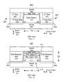
- FIG. 9 depicts an ABS view of an exemplary embodiment of a portion of a magnetic read apparatus 300 .
- the read apparatus 300 may be part of a read head or may be part of a merged head that also includes a write apparatus.
- the read apparatus 300 may be part of a disk drive having a media, a slider and the read apparatus coupled with (fabricated on) the slider.
- the read apparatus 300 may be part of another data storage device. Further, only a portion of the components of the read apparatus 300 are depicted.
- the view shown in FIG. 9 may be for a read apparatus fabricated using the methods 100 and/or 110 in which the ion mills used to define the read sensor are performed at least for the cross-track direction.
- the read apparatus 300 may be analogous to the read apparatus 200 .
- the read apparatus 300 includes shields 302 and 304 , read sensor 310 , capping layer 318 and soft magnetic bias structures 320 .
- the shield-to-shield spacing is SS, while the track width is TW.
- the shields 302 and 304 are shown as monolithic shields, which include only a single layer. However, other structures are possible for the shields 302 and 304 .
- the read sensor 310 may include multiple layers. For example, the layers for a magnetic tunneling junction, spin valve, dual free layer sensor or other read sensor may be present in the read sensor stack 310 .
- the read sensor 310 has a bottom in proximity to (and shown as adjoining) the shield 302 , a top in proximity to (and shown as adjoining) the capping layer 318 or shield 304 and sides.
- the sides form junction angles ⁇ 1 and ⁇ 2 with the bottom of the read sensor 310 .
- the junction angles are each at least seventy-five degrees and not more than one hundred and five degrees. In some embodiments, the junction angles are each at least eighty-five degrees and not more than ninety-five degrees. In the embodiment depicted in FIG.
- the junction angles are less than ninety degrees.
- This configuration results in the top of the read sensor 310 being narrower than the bottom in the cross-track direction.
- larger junction angles are possible.
- the sides of the read sensor 310 are substantially vertical.
- the top of the read sensor 310 may have the same width as the bottom of the read sensor 310 .
- the junction angle(s) are greater than ninety degrees
- the top of the read sensor 310 may be wider than the bottom of the read sensor 310 in the cross-track direction.
- the sidewalls need not be straight.
- the two free layers may be symmetric.
- the middle region of the read sensor may be narrower than the top or the bottom.
- the magnetic bias structures 320 include a side shielding material that has a saturation magnetization and an exchange length.
- the saturation magnetization of the side shielding material is greater than 800 emu/cm 3 .
- the exchange length of the side shielding material is less than five nanometers.
- both the saturation magnetization of the side shielding material is greater than 800 emu/cm 3 and the exchange length of the side shielding material is less than five nanometers. This may be achieved by selection of side shielding materials.
- nanomagnets such as small clusters of Co or Fe particles in an insulating or oxide matrix, such as Hf oxide, may have the reduced exchange length described above.
- Other materials such as Co, Fe, a CoFe alloy such as Co 90 Fe 10 and/or NiFeX, where X is a material such as Cr and/or Ta, may also be used.
- Other materials having the saturation magnetization and exchange length described above may also be used.
- the side magnetic bias structures 320 may consist of only the side shielding material. In some such embodiments, multiple different side shielding materials having the saturation magnetization greater than 800 emu/cm 3 and/or the exchange length less than five nanometers may be used. In other embodiments, the side shielding material may be incorporated in another manner.
- the side magnetic bias structures 320 may include one or more layers of the side shielding material as well as other magnetic or nonmagnetic layers. In such embodiments, the layers of side shielding materials may be ferromagnetically or antiferromagnetically aligned.
- the magnetic read apparatus 300 may have improved performance.
- the large junction angles ⁇ 1 and ⁇ 2 may allow for improved performance of the read sensor 310 .
- stability and/or other magnetic properties may be improved.
- the high junction angle read sensor 310 may be reliably fabricated using the method 100 and/or 110 .
- the side magnetic bias structures 320 may also provide improved side shielding.
- the combination of the (nearly) vertical sidewalls of the read sensor 310 and the side shielding material discussed above may improve the cross-track resolution.
- the side shielding material described above has a lower exchange length and larger magnetization than is typically selected for side shields.
- the improvement in the cross-track resolution for the magnetic read apparatus 300 may be considered surprising.
- FIG. 10 depicts an ABS view of an exemplary embodiment of a read apparatus 300 ′.
- the read apparatus 300 ′ may be part of a read head or may be part of a merged head that also includes a write apparatus.
- the read apparatus 300 ′ may be part of a disk drive having a media, a slider and the read apparatus coupled with (fabricated on) the slider.
- the read apparatus 300 ′ may be part of another data storage device. Further, only a portion of the components of the read apparatus 300 ′ are depicted.
- the view shown in FIG. 10 may be for a read apparatus fabricated using the methods 100 and/or 110 in which the ion mills used to define the read sensor are performed at least for the cross-track direction.
- the head of which the read apparatus 300 ′ is a part is part of a disk drive having a media, a slider and the head coupled with the slider.
- the read apparatus 300 ′ corresponds to the read apparatus 300 . Consequently, analogous components are labeled similarly.
- the read apparatus 300 ′ includes shields 302 and 304 , read sensor 310 , capping layer 318 , nonmagnetic layer 306 and soft magnetic bias structures 320 ′ that are analogous to the shields 302 and 304 , read sensor 310 , capping layer 318 , nonmagnetic layer 306 and soft magnetic bias structures 320 , respectively.
- the magnetic bias structures 320 ′ include magnetic bias layers 330 and 350 and nonmagnetic layer 340 .
- the magnetic moments of the magnetic bias layers 330 and 350 are antiferromagnetically aligned.
- the magnetic moments of the magnetic bias layers 330 and 350 are ferromagnetically aligned.
- One or both of the magnetic bias layers 330 and 350 include the side shielding material that has the saturation magnetization greater than 800 emu/cm 3 and/or the exchange length less than five nanometers.
- the side shielding material(s) may be selected from the material(s) described above.
- only the magnetic layers 330 are formed of the side shielding material(s).
- only the magnetic layers 350 are formed of the side shielding material(s).
- both of the magnetic layers 330 and 350 include the side shielding material(s).
- the magnetic read apparatus 300 ′ may have improved performance analogous to that of the magnetic read apparatus 200 and/or 300 .
- the large junction angles ⁇ 1 and ⁇ 2 may allow for improved performance of the read sensor 310 .
- the high junction angle read sensor 310 may be reliably fabricated using the method 100 and/or 110 .
- the side magnetic bias structures 320 ′, particularly in combination with the large junction angle read sensor 310 may also provide improved side shielding.
- the side shielding material described above has a lower exchange length and larger magnetization than is typically selected for side shields. Thus, the improvement in the cross-track resolution for the magnetic read apparatus 300 ′ may be considered surprising.
- FIG. 11 depicts an ABS view of an exemplary embodiment of a read apparatus 300 ′′.
- the read apparatus 300 ′′ may be part of a read head or may be part of a merged head that also includes a write apparatus.
- the read apparatus 300 ′′ may be part of a disk drive having a media, a slider and the read apparatus coupled with (fabricated on) the slider.
- the read apparatus 300 ′′ may be part of another data storage device. Further, only a portion of the components of the read apparatus 300 ′′ are depicted.
- the view shown in FIG. 11 may be for a read apparatus fabricated using the methods 100 and/or 110 in which the ion mills used to define the read sensor are performed at least for the cross-track direction.
- the head of which the read apparatus 300 ′′ is a part is part of a disk drive having a media, a slider and the head coupled with the slider.
- the read apparatus 300 ′′ corresponds to the read apparatus 300 and/or 300 ′. Consequently, analogous components are labeled similarly.
- the read apparatus 300 ′′ includes shields 302 and 304 , read sensor 310 , capping layer 318 , nonmagnetic layer 306 and soft magnetic bias structures 320 ′′ that are analogous to the shields 302 and 304 , read sensor 310 , capping layer 318 , nonmagnetic layer 306 and soft magnetic bias structures 320 / 320 ′, respectively.
- the magnetic bias structures 320 ′′ include magnetic bias layers 330 ′ and 350 ′.
- the magnetic bias layers 330 ′ and 350 ′ adjoin (share an interface).
- a nonmagnetic layer analogous to the nonmagnetic layer 340 may be included.
- the magnetic moments of the magnetic bias layers 330 ′ and 350 ′ are ferromagnetically aligned.
- One or both of the magnetic bias layers 330 ′ and 350 ′ include the side shielding material that has the saturation magnetization greater than 800 emu/cm 3 and/or the exchange length less than five nanometers.
- the side shielding material(s) may be selected from the material(s) described above.
- only the magnetic layers 330 ′ are formed of the side shielding material(s). Because a portion of the magnetic bias layers 330 ′ are closer to the read sensor 310 than the magnetic bias layers 350 ′, it may be preferred to use the above-described side shielding materials in at least the magnetic bias layer 330 ′. In other embodiments, only the magnetic layers 350 ′ are formed of the side shielding material(s). In still other embodiments both of the magnetic layers 330 ′ and 350 ′ include the side shielding material(s).
- the magnetic read apparatus 300 ′′ may have improved performance analogous to that of the magnetic read apparatus 200 , 300 and/or 300 ′.
- the large junction angles ⁇ 1 and ⁇ 2 may allow for improved performance of the read sensor 310 .
- the high junction angle read sensor 310 may be reliably fabricated using the method 100 and/or 110 .
- the side magnetic bias structures 320 ′′, particularly in combination with the large junction angle read sensor 310 may also provide improved side shielding.
- the side shielding material described above has a lower exchange length and larger magnetization than is typically selected for side shields. Thus, the improvement in the cross-track resolution for the magnetic read apparatus 300 ′′ may be considered surprising.
- FIG. 12 depicts an ABS view of an exemplary embodiment of a read apparatus 400 .
- the read apparatus 400 may be part of a read head or may be part of a merged head that also includes a write apparatus.
- the read apparatus 400 may be part of a disk drive having a media, a slider and the read apparatus coupled with (fabricated on) the slider.
- the read apparatus 400 may be part of another data storage device. Further, only a portion of the components of the read apparatus 400 are depicted.
- the view shown in FIG. 12 may be for a read apparatus fabricated using the methods 100 and/or 110 in which the ion mills used to define the read sensor are performed at least for the cross-track direction.
- the head of which the read apparatus 400 is a part is part of a disk drive having a media, a slider and the head coupled with the slider.
- the read apparatus 400 may correspond to the read apparatuses 200 , 300 , 300 ′ and/or 300 ′′. Consequently, analogous components are labeled similarly.
- the read apparatus 400 includes shields 402 and 404 , read sensor 410 , capping layer 418 , nonmagnetic layer 406 and magnetic bias structures 420 that are analogous to the shields 302 and 304 , read sensor 310 , capping layer 318 , nonmagnetic layer 306 and soft magnetic bias structures 320 / 320 ′/ 320 ′′, respectively.
- the magnetic bias structures 420 may be monolithic, as shown in FIG. 12 . Alternatively, the magnetic bias structures 420 or may include multiple layers, for example as shown in FIGS. 10 and 11 .
- the magnetic read apparatus 400 also includes sensor 410 .
- the read sensor 410 includes an antiferromagnetic (AFM) layer 411 , a reference layer 412 adjoining the AFM layer 411 , a nonmagnetic spacer layer 414 and a free layer 416 .
- the nonmagnetic spacer layer 414 may be a tunneling barrier layer, a conductive nonmagnetic layer or another analogous layer.
- the free layer 416 and reference layer 412 are magnetic and may include one or more sublayers.
- the AFM layer 411 may be a multilayer or a single layer.
- the magnetic read apparatus 400 may have improved performance analogous to that of the magnetic read apparatus 200 , 300 , 300 ′ and/or 300 ′′.
- the large junction angles ⁇ 1 and ⁇ 2 may allow for improved performance of the read sensor 410 .
- the free layer 416 may have a larger volume and an attendant improvement in magnetic properties.
- the high junction angle read sensor 410 may be reliably fabricated using the method 100 and/or 110 .
- the side magnetic bias structures 420 particularly in combination with the large junction angle read sensor 410 , may also provide improved side shielding for the reasons discussed above. Thus, performance of the read apparatus 400 may be enhanced.
- FIG. 13 depicts an ABS view of an exemplary embodiment of a read apparatus 400 ′.
- the read apparatus 400 ′ may be part of a read head or may be part of a merged head that also includes a write apparatus.
- the read apparatus 400 ′ may be part of a disk drive having a media, a slider and the read apparatus coupled with (fabricated on) the slider.
- the read apparatus 400 ′ may be part of another data storage device. Further, only a portion of the components of the read apparatus 400 ′ are depicted.
- the view shown in FIG. 13 may be for a read apparatus fabricated using the methods 100 and/or 110 in which the ion mills used to define the read sensor are performed at least for the cross-track direction.
- the head of which the read apparatus 400 ′ is a part is part of a disk drive having a media, a slider and the head coupled with the slider.
- the read apparatus 400 ′ may correspond to the read apparatuses 200 , 300 , 300 ′, 300 ′′ and/or 400 . Consequently, analogous components are labeled similarly.
- the read apparatus 400 ′ includes shields 402 and 404 , read sensor 410 ′, capping layer 418 , nonmagnetic layer 406 and magnetic bias structures 420 that are analogous to the shields 402 and 404 , read sensor 410 , capping layer 418 , nonmagnetic layer 406 and soft magnetic bias structures 420 , respectively.
- the magnetic bias structures 420 may be monolithic, as shown in FIG. 13 . Alternatively, the magnetic bias structures 420 or may include multiple layers, for example as shown in FIGS. 10 and 11 .
- the magnetic read apparatus 400 ′ also includes sensor 410 ′. In the embodiment shown, the read sensor 410 ′ is a dual free layer read sensor. Thus, the read sensor 410 ′ includes a first free layer 416 A, a nonmagnetic spacer layer 414 and a second free layer 416 B.
- the nonmagnetic spacer layer 414 may be a tunneling barrier layer, a conductive nonmagnetic layer or another analogous layer.
- the free layers 416 A and 416 B are magnetic and may include one or more sublayers.
- the magnetic layers 416 A and 416 B may be desired to be biased in a scissor mode.
- the magnetic read apparatus 400 ′ may include a rear magnetic bias structure (not shown in FIG. 13 ).
- the read sensor 410 ′ is between the rear bias structure and the ABS.
- the sidewalls for the read sensor 410 ′ need not be.
- the two free layers 416 A and 416 B may be symmetric.
- the middle region of the read sensor 410 ′ may be narrower than the top or the bottom.
- the magnetic read apparatus 400 ′ may have improved performance analogous to that of the magnetic read apparatus 200 , 300 , 300 ′, 300 ′′ and/or 400 .
- the large junction angles ⁇ 1 and ⁇ 2 may allow for improved performance of the read sensor 410 ′.
- the free layers 416 A and 416 B may have a larger volume and an attendant improvement in magnetic properties.
- the high junction angle read sensor 410 ′ may be reliably fabricated using the method 100 and/or 110 .
- the side magnetic bias structures 420 particularly in combination with the large junction angle read sensor 410 ′, may also provide improved side shielding for the reasons discussed above. Thus, performance of the read apparatus 400 ′ may be enhanced.
- the apparatuses 200 , 300 , 300 ′, 300 ′′, 400 and/or 400 ′ may be fabricated.
- the benefits of one or more of the apparatuses 200 , 300 , 300 ′, 300 ′′, 400 , and/or 400 ′ may be achieved.
- the formation of the read sensors and the configuration of the magnetic bias structures may improve reading and side shielding.
- the benefits of the methods 100 and 110 and one or more of the read apparatuses 200 , 300 , 300 ′, 300 ′′, 400 and/or 400 ′ may be attained.
Abstract
Description
Claims (9)
Priority Applications (1)
| Application Number | Priority Date | Filing Date | Title |
|---|---|---|---|
| US14/949,155 US9812155B1 (en) | 2015-11-23 | 2015-11-23 | Method and system for fabricating high junction angle read sensors |
Applications Claiming Priority (1)
| Application Number | Priority Date | Filing Date | Title |
|---|---|---|---|
| US14/949,155 US9812155B1 (en) | 2015-11-23 | 2015-11-23 | Method and system for fabricating high junction angle read sensors |
Publications (1)
| Publication Number | Publication Date |
|---|---|
| US9812155B1 true US9812155B1 (en) | 2017-11-07 |
Family
ID=60189629
Family Applications (1)
| Application Number | Title | Priority Date | Filing Date |
|---|---|---|---|
| US14/949,155 Active US9812155B1 (en) | 2015-11-23 | 2015-11-23 | Method and system for fabricating high junction angle read sensors |
Country Status (1)
| Country | Link |
|---|---|
| US (1) | US9812155B1 (en) |
Cited By (3)
| Publication number | Priority date | Publication date | Assignee | Title |
|---|---|---|---|---|
| US10103322B1 (en) * | 2017-03-22 | 2018-10-16 | Headway Technologies Inc. | Method to remove sidewall damage after MTJ etching |
| US20200227473A1 (en) * | 2019-01-14 | 2020-07-16 | United Microelectronics Corp. | Mram structure and method of fabricating the same |
| US11514930B1 (en) * | 2021-06-25 | 2022-11-29 | Western Digital Technologies, Inc. | Soft bias side shield stabilized by hard bias for read head design |
Citations (554)
| Publication number | Priority date | Publication date | Assignee | Title |
|---|---|---|---|---|
| US5529671A (en) | 1994-07-27 | 1996-06-25 | Litton Systems, Inc. | Apparatus and method for ion beam polishing and for in-situ ellipsometric deposition of ion beam films |
| US6016290A (en) | 1999-02-12 | 2000-01-18 | Read-Rite Corporation | Read/write head with shifted waveguide |
| US6018441A (en) | 1998-06-08 | 2000-01-25 | Read-Rite Corporation | Disk drive pivot bearing and actuator arm assembly |
| US6025988A (en) | 1998-12-17 | 2000-02-15 | Read-Rite Corporation | Interconnect adapter and head suspension assembly |
| US6025978A (en) | 1996-12-20 | 2000-02-15 | Read-Rite Smi Corporation | Composite type thin-film magnetic head with improved recording characteristics and high resolution |
| US6032353A (en) | 1997-05-15 | 2000-03-07 | Read-Rite Corporation | Magnetic head with low stack height and self-aligned pole tips |
| US6034851A (en) | 1998-04-07 | 2000-03-07 | Read-Rite Corporation | Shorting bar and test clip for protecting magnetic heads from damage caused by electrostatic discharge during manufacture |
| US6033532A (en) | 1996-02-27 | 2000-03-07 | Read-Rite Smi Corporation | Oxide film fabrication method and electronic device |
| US6043959A (en) | 1998-03-23 | 2000-03-28 | Read-Rite Corporation | Inductive write head formed with flat yoke and merged with magnetoresistive read transducer |
| US6046885A (en) | 1998-04-03 | 2000-04-04 | Intri-Plex Technologies, Inc. | Base plate suspension assembly in a hard disk drive with step in flange |
| US6049650A (en) | 1998-04-17 | 2000-04-11 | Seagate Technology, Inc. | Structure for micro-machine optical tooling and method for making and using |
| US6054023A (en) | 1997-12-22 | 2000-04-25 | International Business Machines Corporation | Method of making inverted merged MR head with track width defining first pole tip component constructed on a side wall |
| US6055138A (en) | 1998-05-06 | 2000-04-25 | Read-Rite Corporation | Thin film pedestal pole tips write head having narrower lower pedestal pole tip |
| US6058094A (en) | 1996-07-30 | 2000-05-02 | Seagate Technology Inc. | Flying magneto-optical head with a steerable mirror |
| US6073338A (en) | 1997-08-19 | 2000-06-13 | Read-Rite Corporation | Thin film read head with coplanar pole tips |
| US6078479A (en) | 1993-08-10 | 2000-06-20 | Read-Rite Corporation | Magnetic tape head with flux sensing element |
| US6081499A (en) | 1997-05-05 | 2000-06-27 | Seagate Technology, Inc. | Magneto-optical data storage system having an optical-processing flying head |
| US6094803A (en) | 1999-01-21 | 2000-08-01 | Read-Rite Corporation | Wafer processing techniques for near field magneto-optical head |
| US6099362A (en) | 1996-01-18 | 2000-08-08 | Read-Rite Corporation | Apparatus and method for testing magnetic disk drive components |
| US6103073A (en) | 1996-07-15 | 2000-08-15 | Read-Rite Corporation | Magnetic thin film head zero throat pole tip definition |
| US6108166A (en) | 1998-03-12 | 2000-08-22 | Read-Rite Corporation | Current-pinned spin valve sensor |
| US6118629A (en) | 1997-07-28 | 2000-09-12 | Read-Rite Corporation | Magnetic head with aligned pole tips and pole layers formed of high magnetic moment material |
| US6118638A (en) | 1998-11-02 | 2000-09-12 | Read-Rite Corporation | CPP magnetoresistive device and method for making same |
| US6125018A (en) | 1997-06-10 | 2000-09-26 | Read-Rite Smi Corporation | Composite type thin-film magnetic head |
| US6130779A (en) | 1998-07-06 | 2000-10-10 | Read-Rite Corporation | Near field magneto-optical head made using wafer processing techniques |
| US6134089A (en) | 1999-03-11 | 2000-10-17 | Read-Rite Corporation | Current perpendicular to plane magnetoresistive device with low resistance lead |
| US6137661A (en) | 1998-10-19 | 2000-10-24 | Read-Rite Corporation | System for providing a magnetoresistive head having higher efficiency |
| US6136166A (en) | 1998-03-27 | 2000-10-24 | Read-Rite Corporation | Apparatus for producing a uniform magnetic field over a large surface area of a wafer |
| US6137662A (en) | 1998-04-07 | 2000-10-24 | Read-Rite Corporation | Magnetoresistive sensor with pinned SAL |
| US6160684A (en) | 1998-11-12 | 2000-12-12 | Read-Rite Corporation | Head suspension having tabs and force isolation welds for gram load reduction during swaging |
| US6163426A (en) | 1996-04-23 | 2000-12-19 | Read Rite Corporation | Magnetoresistive head with minimal electromigration |
| US6166891A (en) | 1997-06-30 | 2000-12-26 | Read-Rite Corporation | Magnetoresistive sensor for high temperature environment using iridium manganese |
| US6173486B1 (en) | 1997-03-04 | 2001-01-16 | Read-Rite Corporation | Thin film magnetic head with self-aligned pole tips |
| US6175476B1 (en) | 1998-08-18 | 2001-01-16 | Read-Rite Corporation | Synthetic spin-valve device having high resistivity anti parallel coupling layer |
| US6178150B1 (en) | 1996-07-30 | 2001-01-23 | Seagate Technology Inc. | Offset optics for use with optical heads |
| US6178066B1 (en) | 1998-05-27 | 2001-01-23 | Read-Rite Corporation | Method of fabricating an improved thin film device having a small element with well defined corners |
| US6178070B1 (en) | 1999-02-11 | 2001-01-23 | Read-Rite Corporation | Magnetic write head and method for making same |
| US6181525B1 (en) | 1998-09-23 | 2001-01-30 | Read-Rite Corporation | Read/write head with a limited range of motion relative to a load beam |
| US6181485B1 (en) | 1999-06-23 | 2001-01-30 | Read-Rite Corporation | High numerical aperture optical focusing device for use in data storage systems |
| US6185081B1 (en) | 1999-06-30 | 2001-02-06 | Read-Rite Corporation | Bias layers which are formed on underlayers promoting in-plane alignment of the c-axis of cobalt used in magnetoresistive transducers |
| US6185077B1 (en) | 1999-01-06 | 2001-02-06 | Read-Rite Corporation | Spin valve sensor with antiferromagnetic and magnetostatically coupled pinning structure |
| US6185051B1 (en) | 1999-06-23 | 2001-02-06 | Read-Rite Corporation | High numerical aperture optical focusing device for use in data storage systems |
| US6188549B1 (en) | 1997-12-10 | 2001-02-13 | Read-Rite Corporation | Magnetoresistive read/write head with high-performance gap layers |
| US6190764B1 (en) | 1998-11-23 | 2001-02-20 | Read-Rite Corporation | Inductive write head for magnetic data storage media |
| US6193584B1 (en) | 1999-05-27 | 2001-02-27 | Read-Rite Corporation | Apparatus and method of device stripe height control |
| US6195229B1 (en) | 1998-01-30 | 2001-02-27 | Read-Rite Corporation | Thin film MR head and method of making wherein pole trim takes place at the wafer level |
| US6198608B1 (en) | 1999-03-18 | 2001-03-06 | Read-Rite Corporation | MR sensor with blunt contiguous junction and slow-milling-rate read gap |
| US6198609B1 (en) | 1998-11-09 | 2001-03-06 | Read-Rite Corporation | CPP Magnetoresistive device with reduced edge effect and method for making same |
| US6201673B1 (en) | 1999-04-02 | 2001-03-13 | Read-Rite Corporation | System for biasing a synthetic free layer in a magnetoresistance sensor |
| US6204998B1 (en) | 1996-03-28 | 2001-03-20 | Read-Rite Corporation | Multi-tapped coil having tapped segments cascaded for amplification for improving signal-to-noise ratio |
| US6204999B1 (en) | 1998-12-23 | 2001-03-20 | Read-Rite Corporation | Method and system for providing a write head having a conforming pole structure |
| US6212153B1 (en) | 1998-07-06 | 2001-04-03 | Read-Rite Corporation | High NA solid catadioptric focusing device having a flat kinoform phase profile |
| US6215625B1 (en) | 1999-01-04 | 2001-04-10 | Read-Rite Corporation | Apparatus and method for adhesive bridge suspension attachment |
| US6219205B1 (en) | 1995-10-10 | 2001-04-17 | Read-Rite Corporation | High density giant magnetoresistive transducer with recessed sensor |
| US6221218B1 (en) | 1998-11-23 | 2001-04-24 | Read-Rite Corporation | Method of forming an inductive write head for magnetic data storage media |
| US6222707B1 (en) | 1998-12-28 | 2001-04-24 | Read-Rite Corporation | Bottom or dual spin valve having a seed layer that results in an improved antiferromagnetic layer |
| US6229782B1 (en) | 1998-07-06 | 2001-05-08 | Read-Rite Corporation | High numerical aperture optical focusing device for use in data storage systems |
| US6233116B1 (en) | 1998-11-13 | 2001-05-15 | Read-Rite Corporation | Thin film write head with improved laminated flux carrying structure and method of fabrication |
| US6237215B1 (en) | 1997-02-07 | 2001-05-29 | Read Rite Corporation | Test fixture for positioning and testing a magnetic head |
| US6252743B1 (en) | 1998-11-02 | 2001-06-26 | Read-Rite Corporation | Read/write positioning arm with interspaced amplifier chips |
| US6255721B1 (en) | 1997-08-07 | 2001-07-03 | Read-Rite Corporation | Method and tool for handling micro-mechanical structures |
| US6258468B1 (en) | 1998-12-22 | 2001-07-10 | Read-Rite Corporation | AMR read sensor structure and method with high magnetoresistive coefficient |
| US6266216B1 (en) | 1996-11-08 | 2001-07-24 | Read-Rite Corporation | Inductive/MR composite type thin-film magnetic head with NLTS reduction |
| US6271604B1 (en) | 1999-05-10 | 2001-08-07 | Western Digital Corporation | Integrated computer module having a data integrity latch |
| US6275354B1 (en) | 1998-01-21 | 2001-08-14 | Read-Rite Corporation | Magnetic head with a toroidal coil encompassing only one yoke layer |
| US6277505B1 (en) | 1999-01-21 | 2001-08-21 | Read-Rite Corporation | Read sensor with improved thermal stability and manufacturing method therefor |
| US6282056B1 (en) | 1999-04-08 | 2001-08-28 | Read-Rite Corporation | Tapered stitch pole writer for high density magnetic recording |
| US6296955B1 (en) | 1999-05-24 | 2001-10-02 | Read-Rite Corporation | High moment and high permeability transducer structures and formation |
| US6297955B1 (en) | 1999-03-31 | 2001-10-02 | Western Digital Ventures, Inc. | Host assembly for an integrated computer module |
| US6304414B1 (en) | 1999-07-20 | 2001-10-16 | Read-Rite Corporation | Thin film magnetic write head having an ultra-low stack height |
| US6307715B1 (en) | 1996-08-30 | 2001-10-23 | Read-Rite Corporation | Head suspension having reduced torsional vibration |
| US6310746B1 (en) | 1999-06-23 | 2001-10-30 | Read-Rite Corporation | Piezoelectric vibration damping for disk drives |
| US6310750B1 (en) | 1999-10-20 | 2001-10-30 | Read-Rite Corporation | Disk drive actuator arm with microactuated read/write head positioning |
| US6317290B1 (en) | 1999-08-31 | 2001-11-13 | Read-Rite Corporation | Advance pole trim writer with moment P1 and low apex angle |
| US6317297B1 (en) | 1999-10-06 | 2001-11-13 | Read-Rite Corporation | Current pinned dual spin valve with synthetic pinned layers |
| US6322911B1 (en) | 1999-02-01 | 2001-11-27 | Read-Rite Corporation | Spin-valve magnetic resistance sensor and thin-film magnetic head |
| US6330136B1 (en) | 1998-10-14 | 2001-12-11 | Read-Rite Corporation | Magnetic read sensor with SDT tri-layer and method for making same |
| US6330137B1 (en) | 1999-06-11 | 2001-12-11 | Read-Rite Corporation | Magnetoresistive read sensor including a carbon barrier layer and method for making same |
| US6333830B2 (en) | 1998-11-09 | 2001-12-25 | Read-Rite Corporation | Low resistance coil structure for high speed writer |
| US6340533B1 (en) | 1998-09-09 | 2002-01-22 | Read-Rite Corporation | Spin-valve magnetoresistance sensor and thin film magnetic head |
| US6349014B1 (en) | 1999-05-14 | 2002-02-19 | Read-Rite Corporation | Magnetic read/write device with insulated coil layer recessed into pole |
| US6351355B1 (en) | 1999-02-09 | 2002-02-26 | Read-Rite Corporation | Spin valve device with improved thermal stability |
| US6353318B1 (en) | 2000-03-10 | 2002-03-05 | Read-Rite Corporation | Magnetoresistive sensor having hard biased current perpendicular to the plane sensor |
| US6353511B1 (en) | 1999-06-15 | 2002-03-05 | Read-Rite Corporation | Thin film write head for improved high speed and high density recording |
| US6356412B1 (en) | 1999-09-30 | 2002-03-12 | Read-Rite Corporation | Air bearing facilitating load/unload of a magnetic read/write head |
| US6359779B1 (en) | 1999-04-05 | 2002-03-19 | Western Digital Ventures, Inc. | Integrated computer module with airflow accelerator |
| US6369983B1 (en) | 1999-08-13 | 2002-04-09 | Read-Rite Corporation | Write head having a dry-etchable antireflective intermediate layer |
| US6377535B1 (en) | 1998-07-06 | 2002-04-23 | Read-Rite Corporation | High numerical aperture optical focusing device having a conical incident facet and a parabolic reflector for use in data storage systems |
| US6376964B1 (en) | 2001-05-16 | 2002-04-23 | Read-Rite Corporation | Collocated rotating flexure microactuator for dual-stage servo in disk drives |
| US6381095B1 (en) | 1999-08-31 | 2002-04-30 | Read-Rite Corporation | High performance thin film magnetic write element having high Bsat poles and method for making same |
| US6381105B1 (en) | 1999-10-22 | 2002-04-30 | Read-Rite Corporation | Hybrid dual spin valve sensor and method for making same |
| US6389499B1 (en) | 1999-06-09 | 2002-05-14 | Western Digital Ventures, Inc. | Integrated computer module |
| US6392850B1 (en) | 1997-04-03 | 2002-05-21 | Read-Rite Corporation | Magnetoresistive transducer having a common magnetic bias using assertive and complementary signals |
| US6395388B1 (en) | 1992-10-30 | 2002-05-28 | Kabushiki Kaisha Toshiba | Magnetoresistance effect element |
| US6396660B1 (en) | 1999-08-23 | 2002-05-28 | Read-Rite Corporation | Magnetic write element having a thermally dissipative structure |
| US6400526B2 (en) | 1999-05-26 | 2002-06-04 | Read-Rite Corporation | Advanced writer for chip-on-load beam |
| US6399179B1 (en) | 1998-04-03 | 2002-06-04 | Intri-Plex Technologies, Inc. | Base plate for suspension assembly in hard disk drive with stress isolation |
| US6404706B1 (en) | 1999-02-12 | 2002-06-11 | Read-Rite Corporation | Laser mounting for a thermally assisted GMR head |
| US6404601B1 (en) | 2000-01-25 | 2002-06-11 | Read-Rite Corporation | Merged write head with magnetically isolated poletip |
| US6411522B1 (en) | 1999-04-01 | 2002-06-25 | Western Digital Ventures, Inc. | Integrated computer module with EMI shielding plate |
| US6410170B1 (en) | 1999-05-20 | 2002-06-25 | Read-Rite Corporation | High resistivity FeXN sputtered films for magnetic storage devices and method of fabrication |
| US6418000B1 (en) | 1999-01-21 | 2002-07-09 | Read-Rite Corporation | Dual, synthetic spin valve sensor using current pinning |
| US6418048B1 (en) | 2001-08-15 | 2002-07-09 | Read-Rite Corporation | Spin-dependent tunneling sensor suitable for a magnetic memory |
| US6417999B1 (en) | 2000-02-04 | 2002-07-09 | Read-Rite Corporation | Magnetoresistive head stabilized structure and method of fabrication thereof |
| US6417998B1 (en) | 1999-03-23 | 2002-07-09 | Read-Rite Corporation | Ultra small advanced write transducer and method for making same |
| US6421212B1 (en) | 1999-09-21 | 2002-07-16 | Read-Rite Corporation | Thin film read head structure with improved bias magnet-to-magnetoresistive element interface and method of fabrication |
| US6424505B1 (en) | 1999-05-06 | 2002-07-23 | Read-Rite Corporation | Method and system for providing electrostatic discharge protection for flex-on suspension, trace-suspension assembly, or cable-on suspension |
| US6430009B1 (en) | 1999-05-06 | 2002-08-06 | Read-Rite Smi Corporation | Magnetic head shield pole with nonmagnetic separation film between transition portion and shield portion |
| US6433970B1 (en) | 1999-06-07 | 2002-08-13 | Read-Rite Corporation | Structure and method for redeposition free thin film CPP read sensor fabrication |
| US6433968B1 (en) | 2000-05-02 | 2002-08-13 | Read-Rite Corporation | Merged read/write head and method of fabricating same |
| US6430806B1 (en) | 2000-06-23 | 2002-08-13 | Read-Rite Corporation | Method for manufacturing an inductive write element employing bi-layer photoresist to define a thin high moment pole pedestal |
| US6433965B1 (en) | 2000-03-02 | 2002-08-13 | Read-Rite Corporation | Laminated carbon-containing overcoats for information storage system transducers |
| US6437945B1 (en) | 1999-12-28 | 2002-08-20 | Read-Rite Corporation | Airflow assisted ramp loading and unloading of sliders in hard disk drives |
| US6445542B1 (en) | 2000-03-06 | 2002-09-03 | Read-Rite Corporation | Air bearing slider |
| US6445554B1 (en) | 2000-03-10 | 2002-09-03 | Read-Rite Corporation | Method and system for providing edge-junction TMR for high areal density magnetic recording |
| US6445536B1 (en) | 1998-08-27 | 2002-09-03 | Read-Rite Corporation | Dielectric stencil-defined write head for MR, GMR, and spin valve high density recording heads |
| US6445553B2 (en) | 1999-04-02 | 2002-09-03 | Read-Rite Corporation | Method and system for fabricating a high density magnetoresistive device |
| US6448765B1 (en) | 1999-10-28 | 2002-09-10 | Read-Rite Corporation | Microscopic tips having stable magnetic moments and disposed on cantilevers for sensing magnetic characteristics of adjacent structures |
| US6447935B1 (en) | 1999-11-23 | 2002-09-10 | Read-Rite Corporation | Method and system for reducing assymetry in a spin valve having a synthetic pinned layer |
| US6451514B1 (en) | 1998-11-27 | 2002-09-17 | Read-Rite Corporation | Method for formation of upper magnetic pole layer of thin film magnetic head, method of forming miniature block pattern with high aspect ratio on bottom part of step on surface with step, and thin film magnetic head |
| US6452742B1 (en) | 1999-09-02 | 2002-09-17 | Read-Rite Corporation | Thin film write having reduced resistance conductor coil partially recessed within middle coat insulation |
| US6452765B1 (en) | 1998-11-18 | 2002-09-17 | Read-Rite Corporation | CoNbTi as high resistivity SAL material for high-density MR |
| US6456465B1 (en) | 1999-11-09 | 2002-09-24 | Read-Rite Corporation | Vertical giant magnetoresistance sensor using a recessed shield |
| US6462920B1 (en) | 1998-12-23 | 2002-10-08 | Read-Rite Corporation | Method and system for reducing MR head instability |
| US6466401B1 (en) | 1999-06-02 | 2002-10-15 | Read-Rite Corporation | Thin film write head with interlaced coil winding and method of fabrication |
| US6466402B1 (en) | 1999-06-18 | 2002-10-15 | Read-Rite Corporation | Compact MR write structure |
| US6469877B1 (en) | 1999-06-15 | 2002-10-22 | Read-Rite Corporation | Spin valve device with improved exchange layer defined track width and method of fabrication |
| US6477019B2 (en) | 1998-10-08 | 2002-11-05 | Read-Rite Smi Corporation | Thin film magnetic head including nonmagnetic and magnetic layers with similar milling rates |
| US6479096B1 (en) | 1999-12-03 | 2002-11-12 | Read-Rite Corporation | Method for manufacturing a GMR spin valve having a smooth interface between magnetic and non-magnetic layers |
| US6483662B1 (en) | 1999-07-09 | 2002-11-19 | Read-Rite Corporation | High density multi-coil magnetic write head having a reduced yoke length and short flux rise time |
| US6490125B1 (en) | 1999-04-09 | 2002-12-03 | Read-Rite Corporation | Thin film write head with improved yoke to pole stitch |
| US6496330B1 (en) | 1999-09-09 | 2002-12-17 | Read-Rite Corporation | Magnetic write head having a splitcoil structure |
| US6496334B1 (en) | 2000-05-26 | 2002-12-17 | Read-Rite Corportion | Data storage and retrieval apparatus with thin film read head having planarized extra gap and shield layers and method of fabrication thereof |
| US6512690B1 (en) | 2001-08-15 | 2003-01-28 | Read-Rite Corporation | High sensitivity common source amplifier MRAM cell, memory array and read/write scheme |
| US6512661B1 (en) | 2000-08-10 | 2003-01-28 | Read-Rite Corporation | Vertical giant magnetoresistance sensor utilizing an insulating bias layer |
| US6512657B2 (en) | 2000-07-17 | 2003-01-28 | Read-Rite Corporation | Head suspension having gram load change reduction and method of assembly |
| US6515791B1 (en) | 2001-04-06 | 2003-02-04 | Read-Rite Corporation | Active reflection and anti-reflection optical switch |
| US6515573B1 (en) | 2000-06-19 | 2003-02-04 | Read-Rite Corporation | Method and system for providing edge-junction TMR utilizing a hard magnet as a pinned layer |
| US6532823B1 (en) | 1999-03-18 | 2003-03-18 | Read-Rite Corporation | Insulator layers for magnetoresistive transducers |
| US6535363B1 (en) | 1999-01-13 | 2003-03-18 | Read-Rite Smi Corporation | Magnetic resistance effect type thin-film magnetic head and method for manufacturing the same |
| US6552874B1 (en) | 2000-05-17 | 2003-04-22 | Read-Rite Corporation | Shared pole magnetic read-write head for achieving optimized erase band width and method of fabricating the same |
| US6552928B1 (en) | 2001-02-23 | 2003-04-22 | Read-Rite Corporation | Read-write control circuit for magnetic tunnel junction MRAM |
| US6577470B1 (en) | 2001-01-25 | 2003-06-10 | Read-Rite Corporation | Method and system for providing a tape head subassembly structure having an integrated wear bar and outrigger rail |
| US6583968B1 (en) | 2001-10-31 | 2003-06-24 | Western Digital Technologies, Inc. | Spindle motor hub having equivalent MR read element bias voltage to mitigate potential between disk and MR read element |
| US6597548B1 (en) | 1998-06-05 | 2003-07-22 | Read-Rite Smi Corporation | Magnetoresistive element and magnetic head |
| US6611398B1 (en) | 1999-08-09 | 2003-08-26 | Quantum Corporation | Tape head with support bars |
| US6618223B1 (en) | 2000-07-18 | 2003-09-09 | Read-Rite Corporation | High speed, high areal density inductive writer |
| US6629357B1 (en) | 1999-02-10 | 2003-10-07 | Read-Rite Smi Corp. | Method of magnetic head manufacture |
| US6633464B2 (en) | 1998-12-09 | 2003-10-14 | Read-Rite Corporation | Synthetic antiferromagnetic pinned layer with Fe/FeSi/Fe system |
| US6636394B1 (en) | 1999-02-23 | 2003-10-21 | Read-Rite Smi Corp. | Spin-valve magnetic resistance sensor and thin-film magnetic head |
| US6639291B1 (en) | 2002-02-06 | 2003-10-28 | Western Digital (Fremont), Inc. | Spin dependent tunneling barriers doped with magnetic particles |
| US6650506B1 (en) | 1999-12-15 | 2003-11-18 | Patrick Risse | Double-sided disk storage using a single configuration of magnetoresistive head |
| US6654195B1 (en) | 1999-04-27 | 2003-11-25 | Western Digital Ventures, Inc. | Disk drive having a register set for providing real time position variables to a host |
| US6657816B1 (en) | 1999-04-09 | 2003-12-02 | Ronald A. Barr | Thin film inductive read/write head with a sloped pole |
| US6661621B1 (en) | 1999-11-19 | 2003-12-09 | Read-Rite Smi Corp. | Compound thin film magnetic head |
| US6661625B1 (en) | 2001-02-20 | 2003-12-09 | Kyusik Sin | Spin-dependent tunneling sensor with low resistance metal oxide tunnel barrier |
| US6674610B1 (en) | 2000-06-16 | 2004-01-06 | Western Digital (Fremont), Inc. | Thin film write head with universal coil design |
| US6680863B1 (en) | 2002-07-09 | 2004-01-20 | Western Digital (Fremont), Inc. | MRAM memory array having merged word lines |
| US6683763B1 (en) | 2001-08-15 | 2004-01-27 | Western Digital (Fremont), Inc. | Method and system for providing a self-aligned electrical contact for a TMR element |
| US6687098B1 (en) | 1999-07-08 | 2004-02-03 | Western Digital (Fremont), Inc. | Top spin valve with improved seed layer |
| US6687178B1 (en) | 2001-02-23 | 2004-02-03 | Western Digital (Fremont), Inc. | Temperature dependent write current source for magnetic tunnel junction MRAM |
| US6691226B1 (en) | 1999-03-16 | 2004-02-10 | Western Digital Ventures, Inc. | Computer system with disk drive having private key validation means for enabling features |
| US6697294B1 (en) | 2001-02-23 | 2004-02-24 | Western Digital (Fremont), Inc. | Designs of reference cells for magnetic tunnel junction (MTJ) MRAM |
| US6700738B1 (en) | 2001-03-16 | 2004-03-02 | Kyusik Sin | Read/write head coil tap having upper and lower portions |
| US6700759B1 (en) | 2000-06-02 | 2004-03-02 | Western Digital (Fremont), Inc. | Narrow track width magnetoresistive sensor and method of making |
| US6704158B2 (en) | 2001-06-05 | 2004-03-09 | Western Digital (Fremont), Inc. | Shear mode multilayered collocated micro-actuator for dual-stage servo controllers in disk drives |
| US6707083B1 (en) | 2002-07-09 | 2004-03-16 | Western Digital (Fremont), Inc. | Magnetic tunneling junction with improved power consumption |
| US6713801B1 (en) | 2002-07-09 | 2004-03-30 | Western Digital (Fremont), Inc. | α-tantalum lead for use with magnetic tunneling junctions |
| US6721149B1 (en) | 2000-02-11 | 2004-04-13 | Western Digital (Fremont), Inc. | Tunneling magnetoresistance spin-valve read sensor with LaNiO3 spacer |
| US6721138B1 (en) | 2001-10-24 | 2004-04-13 | Western Digital (Fremont), Inc. | Inductive transducer with stitched pole tip and pedestal defining zero throat height |
| US6724569B1 (en) | 2000-02-16 | 2004-04-20 | Western Digital (Fremont), Inc. | Thin film writer with multiplayer write gap |
| US6724572B1 (en) | 2002-02-28 | 2004-04-20 | Western Digital, Inc. | Inductive transducer with recessed leading pole layer |
| US6737281B1 (en) | 2002-01-08 | 2004-05-18 | Western Digital (Fremont), Inc. | Method of making transducer with inorganic nonferromagnetic apex region |
| US6744608B1 (en) | 2002-05-14 | 2004-06-01 | Western Digital (Fremont), Inc. | Method and system for making TMR junctions |
| US6747301B1 (en) | 2002-02-06 | 2004-06-08 | Western Digital (Fremont), Inc. | Spin dependent tunneling barriers formed with a magnetic alloy |
| US6751055B1 (en) | 2002-01-08 | 2004-06-15 | Western Digital (Fremont), Inc. | Inductive transducer with reduced pole tip protrusion |
| US6754049B1 (en) | 2001-10-16 | 2004-06-22 | Western Digital (Fremont), Inc. | Transducers for perpendicular recording with inductive cancellation at MR sensor |
| US6757140B1 (en) | 2002-03-19 | 2004-06-29 | Western Digital, Inc. | Electrostatic microelectromechanical (MEM) microactuator for precise read/write head positioning |
| US6760196B1 (en) | 2001-12-12 | 2004-07-06 | Western Digital, Inc. | Microactuator with offsetting hinges and method for high-resolution positioning of magnetic read/write head |
| US6762910B1 (en) | 1999-06-03 | 2004-07-13 | Western Digital (Fremont), Inc. | Data storage and retrieval apparatus with thin film read head having inset extra gap insulation layer and method of fabrication |
| US6765756B1 (en) | 1999-03-12 | 2004-07-20 | Western Digital (Fremont), Inc. | Ultra-short yoke and ultra-low stack height writer and method of fabrication |
| US6775902B1 (en) | 1997-07-28 | 2004-08-17 | Western Digital (Fremont) Inc. | Method of making a magnetic head with aligned pole tips |
| US6778358B1 (en) | 2002-05-01 | 2004-08-17 | Western Digital (Fremont), Inc. | Magnetically soft, high saturation magnetization laminates of iron-cobalt-nitrogen and iron-nickel |
| US6781927B1 (en) | 1996-07-30 | 2004-08-24 | Seagate Technology Llc | Data storage system having an optical processing flying head |
| US6785955B1 (en) | 2001-01-23 | 2004-09-07 | Western Digital (Fremont), Inc. | Method for providing pedestal-defined zero throat writer |
| US6791807B1 (en) | 1998-06-10 | 2004-09-14 | Read-Rite Smi Corporation | Spin-valve magnetic transducing element and magnetic head having free layer with negative magnetostriction |
| US6791793B1 (en) | 2001-09-14 | 2004-09-14 | Western Digital (Fremont), Inc. | Perpendicular recording write head having a recessed magnetic adjunct pole and method of making the same |
| US6798625B1 (en) | 1999-10-28 | 2004-09-28 | Western Digital (Fremont), Inc. | Spin-valve magnetoresistance sensor and thin-film magnetic head |
| US6798616B1 (en) | 2001-07-10 | 2004-09-28 | Western Digital (Fremont), Inc. | Write head architecture for improved manufacturability |
| US6801411B1 (en) | 1999-02-10 | 2004-10-05 | Western Digital (Fremont), Inc. | Dual stripe spin valve sensor without antiferromagnetic pinning layer |
| US6801408B1 (en) | 2000-11-02 | 2004-10-05 | Western Digital (Fremont), Inc. | Data storage and retrieval apparatus with thin film read head having a planar sensor element and an extra gap and method of fabrication thereof |
| US6803615B1 (en) | 2001-02-23 | 2004-10-12 | Western Digital (Fremont), Inc. | Magnetic tunnel junction MRAM with improved stability |
| US6806035B1 (en) | 2002-06-25 | 2004-10-19 | Western Digital (Fremont), Inc. | Wafer serialization manufacturing process for read/write heads using photolithography and selective reactive ion etching |
| US6807030B1 (en) | 2001-12-18 | 2004-10-19 | Western Digital (Fremont), Inc. | Enclosed piezoelectric microactuators coupled between head and suspension |
| US6807332B1 (en) | 2000-11-06 | 2004-10-19 | Western Digital (Fremont), Inc. | Piezoelectric actuated optical switch |
| US6809899B1 (en) | 2001-08-20 | 2004-10-26 | Western Digital (Fremont), Inc. | Magnetic heads for perpendicular recording with trapezoidal pole tips |
| US6816345B1 (en) | 2001-09-24 | 2004-11-09 | Western Digital (Fremont), Inc. | Magnetoresistive sensors having submicron track widths and method of making |
| US6829160B1 (en) | 2001-04-06 | 2004-12-07 | Western Digital (Fremont), Inc. | Magnetic ram cell with amplification circuitry and MRAM memory array formed using the MRAM cells |
| US6828897B1 (en) | 1996-08-26 | 2004-12-07 | Western Digital (Fremont), Inc. | Methods and compositions for optimizing interfacial properties of magnetoresistive sensors |
| US6829819B1 (en) | 1999-05-03 | 2004-12-14 | Western Digital (Fremont), Inc. | Method of forming a magnetoresistive device |
| US6859343B1 (en) | 2002-03-19 | 2005-02-22 | Western Digital, Inc. | Hybrid diffuser for minimizing thermal pole tip protrusion and reader sensor temperature |
| US6859997B1 (en) | 2000-09-19 | 2005-03-01 | Western Digital (Fremont), Inc. | Method for manufacturing a magnetic write element |
| US6861937B1 (en) | 2002-06-25 | 2005-03-01 | Western Digital (Fremont), Inc. | Double winding twin coil for thin-film head writer |
| US6870712B2 (en) | 2001-06-05 | 2005-03-22 | Western Digital (Fremont), Inc. | Inductive writer with flat top pole and pedestal defined zero throat |
| US6873494B2 (en) | 2002-04-29 | 2005-03-29 | Western Digital (Fremont), Inc. | Write head with high moment film layer having tapered portion extending beyond write gap layer |
| US6873547B1 (en) | 2001-02-23 | 2005-03-29 | Read Rite Corporation | High capacity MRAM memory array architecture |
| US6879464B2 (en) | 2002-08-16 | 2005-04-12 | Western Digital (Fremont), Inc. | Air bearing having a cavity patch surface coplanar with a leading edge pad surface |
| US6888704B1 (en) | 2003-01-22 | 2005-05-03 | Western Digital (Fremont), Inc. | Method and system for providing high sensitivity giant magnetoresistive sensors |
| US6888184B1 (en) | 2001-02-23 | 2005-05-03 | Western Digital (Fremont), Inc. | Shielded magnetic ram cells |
| US6891702B1 (en) | 2002-10-31 | 2005-05-10 | Western Digital Technologies, Inc. | Method and devices for providing magnetoresistive heads with protection from electrostatic discharge and electric overstress events |
| US6894871B2 (en) | 2002-08-07 | 2005-05-17 | Western Digital (Fremont), Inc. | Technique for reducing pole tip protrusion in a magnetic write head and GMR stripe temperature in an associated read head structure utilizing one or more internal diffuser regions |
| US6909578B1 (en) | 2002-05-30 | 2005-06-21 | Western Digital (Fremont), Inc. | Method and system for reducing thermal pole tip protrusion |
| US6912106B1 (en) | 2002-08-06 | 2005-06-28 | Western Digital (Fremont), Inc. | Writer with a hot seed zero throat and substantially flat top pole |
| US6934113B1 (en) | 2004-03-31 | 2005-08-23 | Western Digital (Fremont), Inc. | Method and system for providing dynamic actuation of a write head using a strain element |
| US6934129B1 (en) | 2002-09-30 | 2005-08-23 | Western Digital (Fremont), Inc. | Magnetoresistive sensor with overlapping lead layers including alpha tantalum and conductive layers |
| US6940688B2 (en) | 2002-10-21 | 2005-09-06 | Western Digital (Fremont), Inc. | Coil inductive writer having a low inductance and short yoke length |
| US6942824B1 (en) | 2002-05-22 | 2005-09-13 | Western Digital (Fremont), Inc. | UV curable and electrically conductive adhesive for bonding magnetic disk drive components |
| US6943993B2 (en) | 2003-02-11 | 2005-09-13 | Western Digital (Fremont), Inc. | Magnetic recording head with a side shield structure for controlling side reading of thin film read sensor |
| US6944938B1 (en) | 1999-05-03 | 2005-09-20 | Western Digital (Fremont), Inc. | Method of forming a magnetoresistive device |
| US6950266B1 (en) | 2002-10-28 | 2005-09-27 | Western Digital (Fremont), Inc. | Active fly height control crown actuator |
| US6958885B1 (en) | 2000-12-21 | 2005-10-25 | Western Digital (Fremont), Inc. | Insulation layer structure for inductive write heads and method of fabrication |
| US6961221B1 (en) | 2001-12-18 | 2005-11-01 | Western Digital (Fremont), Inc. | Piezoelectric microactuators with substantially fixed axis of rotation and magnified stroke |
| US6969989B1 (en) | 2005-03-11 | 2005-11-29 | Western Digital (Fremont), Inc. | Method for characterizing a perpendicular recording head writing pole |
| US6975486B2 (en) | 2002-08-06 | 2005-12-13 | Western Digital (Fremont), Inc. | Thin film write head having a laminated, flat top pole with bottom shaper and method of fabrication |
| US6987643B1 (en) | 2001-10-23 | 2006-01-17 | Western Digital (Fremont), Inc. | Pole structure to relieve adjacent track writing |
| US6989972B1 (en) | 2002-09-30 | 2006-01-24 | Western Digital (Fremont), Inc. | Magnetoresistive sensor with overlapping leads having distributed current |
| US6989962B1 (en) | 2000-09-26 | 2006-01-24 | Western Digital (Fremont), Inc. | Inductive write head having high magnetic moment poles and low magnetic moment thin layer in the back gap, and methods for making |
| US7006327B2 (en) | 2003-02-27 | 2006-02-28 | Western Digital (Fremont), Inc. | Thin film recording head with a buried coil providing a shortened yoke and improved dimension control |
| US7012832B1 (en) | 2003-10-31 | 2006-03-14 | Western Digital (Fremont), Inc. | Magnetic memory cell with plural read transistors |
| US7023658B1 (en) | 2000-02-08 | 2006-04-04 | Western Digital (Fremont), Inc. | Submicron track-width pole-tips for electromagnetic transducers |
| US7027274B1 (en) | 2001-08-30 | 2006-04-11 | Western Digital (Fremont), Inc. | Spin-dependent tunneling read/write sensor for hard disk drives |
| US7026063B2 (en) | 2000-04-11 | 2006-04-11 | Western Digital (Fremont), Inc. | Spin-valve type magnetoresistance sensor and thin-film magnetic head |
| US7027268B1 (en) | 1999-07-08 | 2006-04-11 | Western Digital (Fremont), Inc. | Method and system for providing a dual spin filter |
| US7035046B1 (en) | 2002-03-19 | 2006-04-25 | Western Digital (Fremont), Inc. | System and method for minimizing thermal pole tip protrusion |
| US7041985B1 (en) | 2004-11-12 | 2006-05-09 | Western Digital (Fremont), Inc. | Manipulator for microscopy sample preparation and methods for making and use thereof |
| US7046490B1 (en) | 2000-01-06 | 2006-05-16 | Western Digital (Fremont), Inc. | Spin valve magnetoresistance sensor and thin film magnetic head |
| US7054113B1 (en) | 2001-10-25 | 2006-05-30 | Western Digital (Fremont), Inc. | Reader/writer for magnetic memory |
| US7057857B1 (en) | 2002-12-20 | 2006-06-06 | Western Digital (Fremont), Inc. | Dimple pivot post for a rotary co-located microactuator |
| US7059868B1 (en) | 2000-03-07 | 2006-06-13 | Western Digital (Fremont), Inc. | Connection of trace circuitry in a computer disk drive system |
| US7092195B1 (en) | 2004-05-28 | 2006-08-15 | Western Digital (Fremont), Inc. | Method of using a magnetic write head having an internal heater |
| US7110289B1 (en) | 2004-03-31 | 2006-09-19 | Western Digital (Fremont), Inc. | Method and system for controlling MRAM write current to reduce power consumption |
| US7113366B1 (en) | 2002-11-07 | 2006-09-26 | Western Digital (Fremont), Inc. | Double-nosed inductive transducer with reduced off-track writing |
| US7114241B2 (en) | 1998-11-11 | 2006-10-03 | Western Digital (Fremont), Inc. | Method of manufacturing a magnetic head device |
| US7116517B1 (en) | 2002-12-18 | 2006-10-03 | Western Digital (Fremont), Inc. | Stitched pole write element with a T-shaped pole tip portion |
| US7126790B1 (en) | 2003-11-26 | 2006-10-24 | Western Digital (Fremont), Inc. | Magnetic head for perpendicular recording with magnetic loop providing non-perpendicular write field |
| US7124654B1 (en) | 2004-09-30 | 2006-10-24 | Western Digital (Fremont), Inc. | Method for determining a microactuator range of movement |
| US7126788B1 (en) | 2003-11-26 | 2006-10-24 | Western Digital (Fremont), Inc. | Trailing edge recording magnetic head with reversed double bias coil and deflection pole for perpendicular recording with a non-perpendicular write field |
| US7131346B1 (en) | 2004-10-15 | 2006-11-07 | Western Digital (Fremont), Inc. | Spin stand testing system with fine positioner for head stack assembly |
| US7133253B1 (en) | 2002-06-03 | 2006-11-07 | Western Digital (Fremont), Inc. | Pole tip with sides flared at media-facing surface |
| US7170725B1 (en) | 2004-09-01 | 2007-01-30 | Western Digital (Fremont), Inc. | Magnetic sensor having an aluminum-nitride seed layer for an anti-ferromagnetic layer |
| US7193815B1 (en) | 2004-04-06 | 2007-03-20 | Western Digital (Fremont), Inc. | Shielded pole magnetic head for perpendicular recording |
| US7196880B1 (en) | 1999-07-19 | 2007-03-27 | Western Digital (Fremont), Inc. | Spin valve sensor having a nonmagnetic enhancement layer adjacent an ultra thin free layer |
| US7199974B1 (en) | 2004-02-02 | 2007-04-03 | Western Digital (Fremont), Inc. | Read/write head with reduced pole tip protrusion |
| US7199975B1 (en) | 2004-05-15 | 2007-04-03 | Western Digital (Fremont), Inc. | Magnetic head for perpendicular recording with hard bias structure for write pole tip |
| US7212384B1 (en) | 2004-02-27 | 2007-05-01 | Western Digital (Fremont), Inc. | Magnetic read head with recessed hard bias and current leads |
| US7211339B1 (en) | 2002-08-22 | 2007-05-01 | Western Digital (Fremont), Inc. | Highly conductive lead adjoining MR stripe and extending beyond stripe height at junction |
| US7238292B1 (en) | 2004-07-30 | 2007-07-03 | Western Digital (Fremont), Inc. | Method of fabricating a write element with a reduced yoke length |
| US7239478B1 (en) | 2004-01-31 | 2007-07-03 | Western Digital (Fremont), Inc. | Write element for perpendicular recording in a data storage system |
| US7248433B1 (en) | 2004-02-02 | 2007-07-24 | Western Digital (Fremont), Inc. | Magnetic head with stitched top pole layer and single layer coil or solenoidal coil |
| US7248449B1 (en) | 2004-03-31 | 2007-07-24 | Western Digital (Fremont), Inc. | Magnetoresistive read sensor with reduced effective shield-to-shield spacing |
| US7248431B1 (en) | 2004-04-30 | 2007-07-24 | Yinshi Liu | Method of fabricating a perpendicular recording write head having a gap with two portions |
| US7280325B1 (en) | 2004-03-31 | 2007-10-09 | Western Digital (Fremont), Llc | Ferromagnetic structure including a first section separated from a ferromagnetic layer by an electrically conductive nonmagnetic spacer and a second section elongated relative to the first section in at least one dimension |
| US7286329B1 (en) | 2003-04-02 | 2007-10-23 | Western Digital (Fremont), Llc | GMR sensor with shallow contiguous junction and bias layers aligned with free sensor layers |
| US7284316B1 (en) | 2004-11-17 | 2007-10-23 | Western Digital (Fremont), Llc | Method for forming a hard bias structure in a magnetoresistive sensor |
| US7289303B1 (en) | 2001-04-05 | 2007-10-30 | Western Digital (Fremont), Llc | Spin valve sensors having synthetic antiferromagnet for longitudinal bias |
| US7292409B1 (en) | 2004-02-27 | 2007-11-06 | Western Digital (Fremont), Llc | Magnetic head with thin trailing pedestal layer |
| US7296339B1 (en) | 2004-09-08 | 2007-11-20 | Western Digital (Fremont), Llc | Method for manufacturing a perpendicular magnetic recording head |
| US7307818B1 (en) | 2004-04-30 | 2007-12-11 | Western Digital (Fremont), Llc | Method and system for providing a stable spin filter |
| US7307814B1 (en) | 2002-03-01 | 2007-12-11 | Western Digital (Fremont), Llc | Pedestal defined zero throat writer having a recessed pedestal |
| US7310204B1 (en) | 2003-12-19 | 2007-12-18 | Western Digital (Fremont), Llc | Inductive writer design for using a soft magnetic pedestal having a high magnetic saturation layer |
| US7318947B1 (en) | 2004-08-31 | 2008-01-15 | Western Digital (Fremont), Llc | Method and apparatus for controlling magnetostriction in a spin valve sensor |
| US7333295B1 (en) | 2004-03-31 | 2008-02-19 | Western Digital (Fremont), Llc | Magnetic recording head with high saturation magnetic flux density CoNiFe thin film composition |
| US7342752B1 (en) | 2004-01-31 | 2008-03-11 | Western Digital (Fremont), Llc | Magnetoresistive read head having a bias structure with at least one dusting layer |
| US7349179B1 (en) | 2001-07-16 | 2008-03-25 | Western Digital (Fremont), Llc | Write head for improved manufacturability larger write field and reduced adjacent track erasure |
| US7349170B1 (en) | 2006-04-28 | 2008-03-25 | Western Digital (Fremont), Llc | Method of monitoring operation of a disk drive by analyzing the envelope of a read-back signal in the frequency domain |
| US7363697B1 (en) | 2005-02-18 | 2008-04-29 | Western Digital (Fremont), Llc | Method for manufacturing a group of head gimbal assemblies |
| US7372665B1 (en) | 2005-01-18 | 2008-05-13 | Western Digital (Fremont), Llc | Magnetic recording head with resistive heating element located near the write coil |
| US7371152B1 (en) | 2006-12-22 | 2008-05-13 | Western Digital (Fremont), Llc | Non-uniform subaperture polishing |
| US7379269B1 (en) | 2004-07-30 | 2008-05-27 | Western Digital (Fremont), Llc | Write element with reduced yoke length for ultra-high density writing |
| US7389577B1 (en) | 2007-06-26 | 2008-06-24 | Western Digital (Fremont), Llc | Method to fabricate an ESD resistant tunneling magnetoresistive read transducer |
| US7417832B1 (en) | 2005-04-26 | 2008-08-26 | Western Digital (Fremont), Llc | Magnetoresistive structure having a novel specular and filter layer combination |
| US7419891B1 (en) | 2006-02-13 | 2008-09-02 | Western Digital (Fremont), Llc | Method and system for providing a smaller critical dimension magnetic element utilizing a single layer mask |
| US7428124B1 (en) | 2005-01-18 | 2008-09-23 | Western Digital (Fremont), Llc | Magnetic recording head with resistive heating element and thermal barrier layer |
| US7430098B1 (en) | 2005-01-18 | 2008-09-30 | Western Digital (Fremont), Llc | Perpendicular magnetic recording head with dynamic flying height heating element |
| US7436620B1 (en) | 2007-05-29 | 2008-10-14 | Western Digital (Fremont), Llc | Method for selecting an electrical power to be applied to a head-based flying height actuator |
| US7440220B1 (en) | 2007-05-29 | 2008-10-21 | Western Digital (Fremont), Llc | Method for defining a touch-down power for head having a flying height actuator |
| US7444740B1 (en) | 2005-01-31 | 2008-11-04 | Western Digital (Fremont), Llc | Damascene process for fabricating poles in recording heads |
| US7493688B1 (en) | 2006-02-13 | 2009-02-24 | Western Digital (Fremont), Llc | Method of manufacturing a magnetic recording transducer |
| US7508627B1 (en) | 2006-03-03 | 2009-03-24 | Western Digital (Fremont), Llc | Method and system for providing perpendicular magnetic recording transducers |
| US7522379B1 (en) | 2004-07-30 | 2009-04-21 | Western Digital (Fremont), Llc | Write element with recessed pole and heat sink layer for ultra-high density writing |
| US7522382B1 (en) | 2005-08-22 | 2009-04-21 | Western Digital (Fremont), Llc | Head stack assembly with interleaved flexure tail bond pad rows |
| US7522377B1 (en) | 2002-05-01 | 2009-04-21 | Western Digital (Fremont), Llc | Magnetic write head with high moment magnetic thin film formed over seed layer |
| US7542246B1 (en) | 2006-04-18 | 2009-06-02 | Western Digital (Fremont), Llc | Transducer with pole tip protrusion compensation layer |
| US7551406B1 (en) | 2005-07-01 | 2009-06-23 | Western Digital (Fremont), Llc | Dual electrical lapping guides with common bonding pad |
| US7554767B1 (en) | 2005-07-01 | 2009-06-30 | Western Digital (Fremont), Llc | Electrical lapping guide disposed laterally relative to a shield pedestal |
| US7552523B1 (en) | 2005-07-01 | 2009-06-30 | Western Digital (Fremont), Llc | Method for manufacturing a perpendicular magnetic recording transducer |
| US7583466B2 (en) | 2007-11-15 | 2009-09-01 | Western Digital (Fremont), Llc | Disk drive determining operating fly height by detecting head disk contact from disk rotation time |
| US7595967B1 (en) | 2004-09-07 | 2009-09-29 | Western Digital (Fremont), Llp | Method for fabricating a spacer layer for a magnetoresistive element |
| US20090290264A1 (en) * | 2008-05-23 | 2009-11-26 | Tdk Corporation | Magnetoresistive device of the cpp type, and magnetic disk system |
| US7639457B1 (en) | 2004-02-27 | 2009-12-29 | Western Digital (Fremont), Llc | Magnetic sensor with underlayers promoting high-coercivity, in-plane bias layers |
| US7660080B1 (en) | 2004-04-30 | 2010-02-09 | Western Digital (Fremont), Llc | Read/write head with dynamic flying height control by magnetostriction |
| US7672086B1 (en) | 2004-04-28 | 2010-03-02 | Western Digital (Fremont), Llc | Method and system for providing a magnetic element having a current confined layer |
| US7672080B1 (en) | 2006-09-15 | 2010-03-02 | Western Digital (Fremont), Llc | Laminated perpendicular writer head including amorphous metal |
| US20100053820A1 (en) * | 2008-09-02 | 2010-03-04 | Tdk Corporation | Magnetoresistive element including a pair of ferromagnetic layers coupled to a pair of shield layers |
| US7684160B1 (en) | 2006-02-06 | 2010-03-23 | Western Digital (Fremont), Llc | Magnetoresistive structure having a novel specular and barrier layer combination |
| US7688546B1 (en) | 2006-12-21 | 2010-03-30 | Western Digital (Fremont), Llc | Perpendicular magnetic recording head having nonmagnetic insertion layers |
| US7695761B1 (en) | 2006-12-21 | 2010-04-13 | Western Digital (Fremont), Llc | Method and system for providing a spin tunneling magnetic element having a crystalline barrier layer |
| US7719795B2 (en) | 2006-11-15 | 2010-05-18 | Western Digital (Fremont), Llc | Head having a transducer heater and an air bearing surface with a flow-diversion dam and pressure-relief trough disposed upstream of the transducer |
| US7736823B1 (en) | 2007-05-11 | 2010-06-15 | Western Digital (Fremont), Llc | Method and system for providing optical proximity correction for structures such as a PMR nose |
| US7785666B1 (en) | 2007-12-12 | 2010-08-31 | Western Digital (Fremont), Llc | Methods for fabricating a magnetic recording device |
| US7796356B1 (en) | 2009-05-04 | 2010-09-14 | Western Digital (Fremont), Llc | Head integrated touchdown sensor for hard disk drives |
| US7800858B1 (en) | 2009-05-04 | 2010-09-21 | Western Digital (Fremont), Llc | Differential head integrated touchdown sensors for hard disk drives |
| US7819979B1 (en) | 2005-01-31 | 2010-10-26 | Western Digital (Fremont), Llc | Method and system for cleaning magnetic artifacts using a carbonyl reactive ion etch |
| US7829264B1 (en) | 2007-08-09 | 2010-11-09 | Western Digital (Fremont), Llc | Method and system for providing a microelectronic device using a plurality of focus distances |
| US20100290157A1 (en) | 2009-05-14 | 2010-11-18 | Western Digital (Fremont), Llc | Damascene coil processes and structures |
| US7846643B1 (en) | 2007-11-02 | 2010-12-07 | Western Digital (Fremont), Llc | Method and system for providing a structure in a microelectronic device using a chromeless alternating phase shift mask |
| US7855854B2 (en) | 2007-04-17 | 2010-12-21 | Western Digital (Fremont), Llc | Head with an air bearing surface having a shallow recessed trailing air flow dam |
| US7869160B1 (en) | 2005-04-27 | 2011-01-11 | Western Digital (Fremont), Llc | Perpendicular recording head with shaped pole surfaces for higher linear data densities |
| US7872824B1 (en) | 2007-06-11 | 2011-01-18 | Western Digital (Fremont), Llc | Setting an operating bias current for a magnetoresistive head by computing a target operating voltage |
| US7872833B2 (en) | 2007-04-17 | 2011-01-18 | Western Digital (Fremont) , LLC | Head with a transducer overcoat having a trailing air flow dam that is shallowly recessed from an air bearing surface |
| US7911737B1 (en) | 2007-03-23 | 2011-03-22 | Western Digital (Fremont), Llc | Method and system for providing a PMR head having an antiferromagnetically coupled pole |
| US7910267B1 (en) | 2008-12-12 | 2011-03-22 | Western Digital (Fremont), Llc | Method and system for providing optical proximity correction for structures such as a PMR nose |
| US7911735B1 (en) | 2007-03-09 | 2011-03-22 | Western Digital (Fremont), Llc | Perpendicular magnetic recording head utilizing a nonmagnetic underlayer layer |
| US7916426B2 (en) | 2007-11-30 | 2011-03-29 | Western Digital (Fremont), Llc | Head with an air bearing surface having left and right leading pressurizing steps, each with short and long regions |
| US20110086240A1 (en) | 2009-10-14 | 2011-04-14 | Western Digital (Fremont), Llc | Double patterning hard mask for damascene perpendicular magnetic recording (pmr) writer |
| US7982989B1 (en) | 2009-12-23 | 2011-07-19 | Western Digital (Fremont), Llc | Method and system for measuring magnetic interference width |
| US8008912B1 (en) | 2008-12-16 | 2011-08-30 | Western Digital (Fremont), Llc | Method and system for testing P2 stiffness of a magnetoresistance transducer at the wafer level |
| US8012804B1 (en) | 2009-12-23 | 2011-09-06 | Western Digital (Fremont), Llc | Method and system for mounting lasers on energy assisted magnetic recording heads |
| US8018678B1 (en) | 2008-11-26 | 2011-09-13 | Western Digital (Fremont), Llc | Method for simultaneous electronic lapping guide (ELG) and perpendicular magnetic recording (PMR) pole formation |
| US8015692B1 (en) | 2007-11-07 | 2011-09-13 | Western Digital (Fremont), Llc | Method for providing a perpendicular magnetic recording (PMR) head |
| US8024748B1 (en) | 2009-09-09 | 2011-09-20 | Western Digital Technologies, Inc. | Method and system for coupling a laser with a slider in an energy assisted magnetic recording disk drive |
| US20110279923A1 (en) * | 2010-05-17 | 2011-11-17 | Tdk Corporation | Magnetoresistive element having a pair of side shields |
| US8072705B1 (en) | 2007-05-11 | 2011-12-06 | Western Digital (Fremont), Llc | Method and system for providing a magnetic writer using a BARC |
| US8077557B1 (en) | 2009-05-19 | 2011-12-13 | Western Digital (Fremont), Llc | Multiple aperture VCSEL EAMR heads |
| US8074345B1 (en) | 2009-05-18 | 2011-12-13 | Western Digital (Fremont), Llc | Method of measuring a bevel angle in a write head |
| US8077435B1 (en) | 2008-11-20 | 2011-12-13 | Western Digital (Fremont), Llc | Current perpendicular-to-plane read sensor with back shield |
| US8077434B1 (en) | 2007-11-19 | 2011-12-13 | Western Digital (Fremont), Llc | Perpendicular magnetic recording head having a recessed magnetic base layer |
| US8077418B1 (en) | 2009-03-31 | 2011-12-13 | Western Digital (Fremont), Llc | Reducing thermal protrusion of a near field transducer in an energy assisted magnetic recording head |
| US8079135B1 (en) | 2007-12-13 | 2011-12-20 | Western Digital (Fremont), Llc | Method for providing a perpendicular magnetic recording (PMR) transducer |
| US8091210B1 (en) | 2008-03-05 | 2012-01-10 | Western Digital (Fremont), Llc | Method for providing a structure in magnetic recording transducer |
| US8097846B1 (en) | 2009-02-25 | 2012-01-17 | Western Digital (Fremont), Llc | Metrology and 3D reconstruction of devices in a wafer |
| US8104166B1 (en) | 2003-12-19 | 2012-01-31 | Western Digital (Fremont), Llc | Self-aligned method for fabricating a high density GMR read element |
| US8116171B1 (en) | 2009-11-11 | 2012-02-14 | Western Digital (Fremont), Llc | Method and system for providing energy assisted magnetic recording disk drive using a vertical surface emitting laser |
| US8116043B2 (en) | 2009-12-09 | 2012-02-14 | Western Digital (Fremont), Llc | Method and system for providing a magnetic transducer having an improved read sensor synthetic antiferromagnet |
| US8125856B1 (en) | 2009-11-05 | 2012-02-28 | Western Digital (Fremont), Llc | Method and system for optically coupling a laser with a transducer in an energy assisted magnetic recording disk drive |
| US8134794B1 (en) | 2009-12-23 | 2012-03-13 | Western Digital (Fremont), Llc | Method and system for providing an energy assisted magnetic recording head in a wafer packaging configuration |
| US8136225B1 (en) | 2008-05-15 | 2012-03-20 | Western Digital (Fremont), Llc | Method and system for providing a perpendicular magnetic recording head |
| US8136805B1 (en) | 2008-11-19 | 2012-03-20 | Western Digital (Fremont), Llc | Row bar holder |
| US8136224B1 (en) | 2008-05-15 | 2012-03-20 | Western Digital (Fremont), Llc | Method and system for providing a perpendicular magnetic recording head utilizing a mask having an undercut line |
| US8141235B1 (en) | 2006-06-09 | 2012-03-27 | Western Digital (Fremont), Llc | Method for manufacturing a perpendicular magnetic recording transducers |
| US8146236B1 (en) | 2008-03-28 | 2012-04-03 | Western Digital (Fremont), Llc | Method for providing a perpendicular magnetic recording (PMR) transducer |
| US8151441B1 (en) | 2008-03-27 | 2012-04-10 | Western Digital (Fremont), Llc | Method for providing and utilizing an electronic lapping guide in a magnetic recording transducer |
| US8164760B2 (en) | 2010-03-11 | 2012-04-24 | Western Digital (Fremont), Llc | Method and system for interrogating the thickness of a carbon layer |
| US8164855B1 (en) | 2009-11-06 | 2012-04-24 | Western Digital (Fremont), Llc | Method and system for providing a write pole in an energy assisted magnetic recording disk drive |
| US8164864B2 (en) | 2009-07-16 | 2012-04-24 | Western Digital (Fremont), Llc | Method and system for fabricating magnetic transducers with improved pinning |
| US8165709B1 (en) | 2009-02-26 | 2012-04-24 | Western Digital (Fremont), Llc | Four pad self-calibrating electronic lapping guide |
| US8163185B1 (en) | 2008-03-31 | 2012-04-24 | Western Digital (Fremont), Llc | Method and apparatus for lifting off photoresist beneath an overlayer |
| US8169473B1 (en) | 2008-03-27 | 2012-05-01 | Western Digital (Fremont), Llc | Method and system for exposing a photoresist in a magnetic device |
| US8166631B1 (en) | 2008-08-27 | 2012-05-01 | Western Digital (Fremont), Llc | Method for fabricating a magnetic recording transducer having side shields |
| US8166632B1 (en) | 2008-03-28 | 2012-05-01 | Western Digital (Fremont), Llc | Method for providing a perpendicular magnetic recording (PMR) transducer |
| US8171618B1 (en) | 2009-06-17 | 2012-05-08 | Western Digital (Fremont), Llc | Tunable pole trim processes for fabricating trapezoidal perpendicular magnetic recording (PMR) write poles |
| US20120111826A1 (en) | 2010-11-10 | 2012-05-10 | Western Digital (Fremont), Llc | Damascene process using pvd sputter carbon film as cmp stop layer for forming a magnetic recording head |
| US8179636B1 (en) | 2008-03-05 | 2012-05-15 | Western Digital (Fremont), Llc | Method and system for providing a perpendicular magnetic recording writer |
| US8191237B1 (en) | 2009-05-21 | 2012-06-05 | Western Digital (Fremont), Llc | Method for providing a structure in a magnetic transducer |
| US8194365B1 (en) | 2009-09-03 | 2012-06-05 | Western Digital (Fremont), Llc | Method and system for providing a read sensor having a low magnetostriction free layer |
| US8194366B1 (en) | 2009-10-14 | 2012-06-05 | Western Digital (Fremont), Llc | TMR read head structures with differential stripe heights |
| US8196285B1 (en) | 2008-12-17 | 2012-06-12 | Western Digital (Fremont), Llc | Method and system for providing a pole for a perpendicular magnetic recording head using a multi-layer hard mask |
| US8200054B1 (en) | 2009-04-19 | 2012-06-12 | Western Digital (Fremont), Llc | High efficiency grating coupling for light delivery in EAMR |
| US8203800B2 (en) | 2009-03-05 | 2012-06-19 | Western Digital (Fremont), Llc | Servo design in data storage media |
| US8220140B1 (en) | 2010-09-13 | 2012-07-17 | Western Digital (Fremont), Llc | System for performing bonding a first substrate to a second substrate |
| US8222599B1 (en) | 2009-04-15 | 2012-07-17 | Western Digital (Fremont), Llc | Precise metrology with adaptive milling |
| US8228633B1 (en) | 2008-08-21 | 2012-07-24 | Western Digital (Fremont), Llc | Method and system for providing a magnetic recording transducer having a hybrid moment pole |
| US8225488B1 (en) | 2009-05-22 | 2012-07-24 | Western Digital (Fremont), Llc | Method for providing a perpendicular magnetic recording (PMR) pole |
| US8227023B1 (en) | 2009-05-27 | 2012-07-24 | Western Digital (Fremont), Llc | Method and system for fabricating magnetic transducers with improved pinning |
| US8233248B1 (en) | 2009-09-16 | 2012-07-31 | Western Digital (Fremont), Llc | Method and system for providing a magnetic recording transducer using a line hard mask |
| US8231796B1 (en) | 2008-12-09 | 2012-07-31 | Western Digital (Fremont), Llc | Method and system for providing a magnetic recording transducer having side shields |
| US8248896B1 (en) | 2010-06-24 | 2012-08-21 | Western Digital (Fremont), Llc | Method and system for providing an energy assisted magnetic recording disk drive having improved heat dissipation |
| US8254060B1 (en) | 2009-04-17 | 2012-08-28 | Western Digital (Fremont), Llc | Straight top main pole for PMR bevel writer |
| US20120216378A1 (en) | 2010-03-24 | 2012-08-30 | Wester Digital (Fremont), Llc | Method and system for providing a piezoelectric multilayer |
| US8259539B1 (en) | 2008-12-17 | 2012-09-04 | Western Digital (Fremont), Llc | Integration of a vertical cavity surface emitting laser (VCSEL) on an energy-assisted magnetic recording (EAMR) head |
| US8259410B1 (en) | 2008-05-23 | 2012-09-04 | Western Digital (Fremont), Llc | Method and system for providing a magnetic head using a composite magnetic material in the recording transducer |
| US8257597B1 (en) | 2010-03-03 | 2012-09-04 | Western Digital (Fremont), Llc | Double rie damascene process for nose length control |
| US8262918B1 (en) | 2009-03-25 | 2012-09-11 | Western Digital (Fremont), Llc | Methods of producing damascene main pole for perpendicular magnetic recording head |
| US8264797B2 (en) | 2009-12-21 | 2012-09-11 | Western Digital (Fremont), Llc | Head gimbal assembly having a radial rotary piezoelectric microactuator between a read head and a flexure tongue |
| US8264798B1 (en) | 2010-06-23 | 2012-09-11 | Western Digital (Fremont), Llc | Systems and methods for providing magnetic recording heads adapted for writing shingled tracks |
| US8262919B1 (en) | 2010-06-25 | 2012-09-11 | Western Digital (Fremont), Llc | Method and system for providing a perpendicular magnetic recording pole using multiple chemical mechanical planarizations |
| US8270126B1 (en) | 2008-06-16 | 2012-09-18 | Western Digital (Fremont), Llc | Method and system for providing an improved hard bias structure |
| US20120237878A1 (en) | 2011-03-18 | 2012-09-20 | Western Digital (Fremont), Llc | Method and system for providing a side shield for a perpendicular magnetic recording pole |
| US8279719B1 (en) | 2009-10-01 | 2012-10-02 | Western Digital (Fremont), Llc | Method and system for coupling a laser with a slider in an energy assisted magnetic recording disk drive |
| US8277669B1 (en) | 2009-12-21 | 2012-10-02 | Western Digital (Fremont), Llc | Method and system for providing a perpendicular magnetic recording pole having a leading edge bevel |
| US8276258B1 (en) | 2008-08-26 | 2012-10-02 | Western Digital (Fremont), Llc | Method for fabricating a magnetic recording transducer |
| US8288204B1 (en) | 2011-08-30 | 2012-10-16 | Western Digital (Fremont), Llc | Methods for fabricating components with precise dimension control |
| US8289821B1 (en) | 2010-12-21 | 2012-10-16 | Western Digital (Fremont), Llc | Method and system for pulsing EAMR disk drives |
| US8291743B1 (en) | 2009-05-27 | 2012-10-23 | Western Digital (Fremont), Llc | Method and system for calibrating an electronic lapping guide for a beveled pole in a magnetic recording transducer |
| US8307539B1 (en) | 2009-09-30 | 2012-11-13 | Western Digital (Fremont), Llc | Method for modeling devices in a wafer |
| US8307540B1 (en) | 2011-03-10 | 2012-11-13 | Western Digital (Fremont), Llc | Method for providing an energy assisted magnetic recording (EAMR) transducer |
| US8310901B1 (en) | 2010-06-09 | 2012-11-13 | Western Digital (Fremont), Llc | Method and system for providing separate write and optical modules in an energy assisted magnetic recording disk drive |
| US8308921B1 (en) | 2006-12-21 | 2012-11-13 | Western Digital (Fremont), Llc | Mask for increased uniformity in ion beam deposition |
| US8315019B1 (en) | 2009-03-31 | 2012-11-20 | Western Digital (Fremont), Llc | Method and system for providing an improved magnetoresistive structure utilizing an oxidation buffer layer |
| US8320219B1 (en) | 2010-06-15 | 2012-11-27 | Western Digital (Fremont), Llc | Trailing edge optimized near field transducer |
| US8320076B1 (en) | 2008-06-26 | 2012-11-27 | Western Digital (Fremont), Llc | Method and system for providing a magnetic recording transducer including an assist pole having surfaces angled with respect to the ABS |
| US8320077B1 (en) | 2008-12-15 | 2012-11-27 | Western Digital (Fremont), Llc | Method and system for providing a high moment film |
| US8320722B1 (en) | 2010-04-13 | 2012-11-27 | Western Digital (Fremont), Llc | Non-linear optical grating |
| US8320220B1 (en) | 2011-10-13 | 2012-11-27 | Western Digital (Fremont), Llc | Method and system for providing an energy assisted magnetic recording disk drive having a non-conformal heat spreader |
| US8316527B2 (en) | 2008-04-01 | 2012-11-27 | Western Digital (Fremont), Llc | Method for providing at least one magnetoresistive device |
| US20120298621A1 (en) | 2011-05-25 | 2012-11-29 | Western Digital (Fremont), Llc | Method and system for fabricating a narrow line structure in a magnetic recording head |
| US8325569B1 (en) | 2011-06-27 | 2012-12-04 | Western Digital (Fremont), Llc | EAMR head having improved optical coupling efficiency |
| US8322022B1 (en) | 2010-06-28 | 2012-12-04 | Western Digital (Fremont), Llc | Method for providing an energy assisted magnetic recording head in a wafer packaging configuration |
| US8322023B1 (en) | 2009-11-10 | 2012-12-04 | Western Digital (Fremont), Llc | Method for providing a wrap-around shield for a magnetic recording transducer |
| US8333008B1 (en) | 2005-07-29 | 2012-12-18 | Western Digital (Fremont), Llc | Method for manufacturing a perpendicular magnetic recording transducer |
| US8334093B2 (en) | 2008-10-31 | 2012-12-18 | Western Digital (Fremont), Llc | Method and system for providing a perpendicular magnetic recording head |
| US8336194B2 (en) | 2009-11-03 | 2012-12-25 | Western Digital (Fremont), Llc | Method of fabricating a tunneling magnetoresistive (TMR) reader |
| US8343319B1 (en) | 2008-09-25 | 2013-01-01 | Western Digital (Fremont), Llc | Method and system for providing an improved hard bias structure |
| US8341826B1 (en) | 2010-04-12 | 2013-01-01 | Western Digital (Fremont), Llc | Method for fabricating a magnetic recording transducer using a split seed layer |
| US8343364B1 (en) | 2010-06-08 | 2013-01-01 | Western Digital (Fremont), Llc | Double hard-mask mill back method of fabricating a near field transducer for energy assisted magnetic recording |
| US8351307B1 (en) | 2010-06-04 | 2013-01-08 | Western Digital (Fremont), Llc | Trailing edge optimized near field transducer having non-rectangular pin cross section |
| US8349195B1 (en) | 2008-06-27 | 2013-01-08 | Western Digital (Fremont), Llc | Method and system for providing a magnetoresistive structure using undercut free mask |
| US8357244B1 (en) | 2007-06-28 | 2013-01-22 | Western Digital (Fremont), Llc | Method for lifting off photoresist beneath an overlayer |
| US8373945B1 (en) | 2007-04-23 | 2013-02-12 | Western Digital (Fremont), Llc | Magnetic writer having a split yoke |
| US8375564B1 (en) | 2009-12-08 | 2013-02-19 | Western Digital (Fremont), Llc | Method for fabricating a pole of a magnetic transducer |
| US8375565B2 (en) | 2010-05-28 | 2013-02-19 | Western Digital (Fremont), Llc | Method for providing an electronic lapping guide corresponding to a near-field transducer of an energy assisted magnetic recording transducer |
| US8385157B1 (en) | 2009-09-30 | 2013-02-26 | Western Digital Technologies, Inc. | Method and system for performing EAMR recording at high density using a large thermal spot size |
| US8385158B1 (en) | 2009-10-06 | 2013-02-26 | Western Digital (Fremont), Llc | Method and system for providing a magnetic recording transducer having a planarized near-field transducer and a sloped pole |
| US8381391B2 (en) | 2009-06-26 | 2013-02-26 | Western Digital (Fremont), Llc | Method for providing a magnetic recording transducer |
| US8393073B2 (en) | 2005-01-14 | 2013-03-12 | HGST Netherlands B.V. | Method to control mask profile for read sensor definition |
| US8394280B1 (en) | 2009-11-06 | 2013-03-12 | Western Digital (Fremont), Llc | Resist pattern protection technique for double patterning application |
| US8400731B1 (en) | 2009-04-19 | 2013-03-19 | Western Digital (Fremont), Llc | Write head with variable side shield gaps |
| US8405930B1 (en) | 2011-03-23 | 2013-03-26 | Western Digital (Fremont), Llc | Method and system for providing a transducer having dual, ABS recessed auxiliary poles on opposite sides of a main pole with non-magnetic spacer adjoining back portion of main pole and positioned between auxiliary poles |
| US8404128B1 (en) | 2009-02-23 | 2013-03-26 | Western Digital (Fremont), Llc | Method and system for providing a perpendicular magnetic recording head |
| US8404129B1 (en) | 2010-03-31 | 2013-03-26 | Western Digital (Fremont), Llc | Method and system for providing a curved surface in a magnetic recording head |
| US8409453B1 (en) | 2010-05-12 | 2013-04-02 | Western Digital (Fremont), Llc | Method and system for providing a wrap-around shield using a patterned seed layer |
| US8416540B1 (en) | 2008-06-26 | 2013-04-09 | Western Digital (Fremont), Llc | Method for defining a magnetoresistive junction using multiple mills at a plurality of angles |
| US8413317B1 (en) | 2010-11-12 | 2013-04-09 | Western Digital (Fremont), Llc | Method for fabricating a structure for a microelectric device |
| US8419953B1 (en) | 2011-06-28 | 2013-04-16 | Western Digital (Fremont), Llc | Method and system for removing an antiferromagnetic seed structure |
| US8422176B1 (en) | 2011-11-15 | 2013-04-16 | Western Digital (Fremont), Llc | Method and system for providing a magnetic read transducer having a bilayer magnetic seed layer |
| US8422841B1 (en) | 2010-05-13 | 2013-04-16 | Western Digital (Fremont), Llc | Double optical grating |
| US8419954B1 (en) | 2011-10-31 | 2013-04-16 | Western Digital (Fremont), Llc | Method for providing a side shield for a magnetic recording transducer |
| US8422342B1 (en) | 2010-06-25 | 2013-04-16 | Western Digital (Fremont), Llc | Energy assisted magnetic recording disk drive using a distributed feedback laser |
| US8424192B1 (en) | 2005-08-08 | 2013-04-23 | Western Digital (Fremont), Llc | Method for manufacturing a pole for a magnetic recording head |
| US8437106B2 (en) * | 2010-10-08 | 2013-05-07 | Tdk Corporation | Thin film magnetic head including spin-valve film with free layer magnetically connected with shield |
| US8441756B1 (en) | 2010-12-16 | 2013-05-14 | Western Digital (Fremont), Llc | Method and system for providing an antiferromagnetically coupled writer |
| US8443510B1 (en) | 2009-05-28 | 2013-05-21 | Western Digital (Fremont), Llc | Method for utilizing an electronic lapping guide for a beveled pole in a magnetic recording transducer |
| US8444866B1 (en) | 2010-09-21 | 2013-05-21 | Westen Digital (Fremont), LLC | Method and system for providing a perpendicular magnetic recording pole with a multi-layer side gap |
| US8451556B1 (en) | 2009-12-23 | 2013-05-28 | Western Digital (Fremont), Llc | Method and system for providing a molded capping layer for an energy assisted magnetic recording head |
| US8449948B2 (en) | 2009-09-10 | 2013-05-28 | Western Digital (Fremont), Llc | Method and system for corrosion protection of layers in a structure of a magnetic recording transducer |
| US8451563B1 (en) | 2011-12-20 | 2013-05-28 | Western Digital (Fremont), Llc | Method for providing a side shield for a magnetic recording transducer using an air bridge |
| US8456967B1 (en) | 2011-10-12 | 2013-06-04 | Western Digital (Fremont), Llc | Systems and methods for providing a pole pedestal for microwave assisted magnetic recording |
| US8456966B1 (en) | 2010-12-17 | 2013-06-04 | Western Digital (Fremont), Llc | Method and system for enhancing optical efficiency for an EAMR head |
| US8454846B1 (en) | 2010-06-17 | 2013-06-04 | Western Digital (Fremont), Llc | Method and system for providing a full wrap-around shield using a frame configured wet etch in a damascene process |
| US8456961B1 (en) | 2011-03-22 | 2013-06-04 | Western Digital (Fremont), Llc | Systems and methods for mounting and aligning a laser in an electrically assisted magnetic recording assembly |
| US8456963B1 (en) | 2010-04-12 | 2013-06-04 | Western Digital (Fremont), Llc | Method and system for an energy assisted magnetic recording head having a suspension-mounted laser |
| US8456964B1 (en) | 2010-11-16 | 2013-06-04 | Western Digital (Fremont), Llc | Energy assisted magnetic recording head having a reflector for improving efficiency of the light beam |
| US8462592B1 (en) | 2010-11-17 | 2013-06-11 | Western Digital (Fremont), Llc | Energy-assisted magnetic recording head having waveguide capable of providing small beam spots |
| US8458892B2 (en) | 2010-05-11 | 2013-06-11 | Western Digital (Fremont), Llc | Method for providing a perpendicular magnetic recording transducer using a low energy mill |
| US8480911B1 (en) | 2011-06-30 | 2013-07-09 | Western Digital (Fremont), Llc | Method and system for providing a read sensor in a magnetic recording transducer using focused ion beam scan polishing |
| US8486285B2 (en) | 2009-08-20 | 2013-07-16 | Western Digital (Fremont), Llc | Damascene write poles produced via full film plating |
| US8486286B1 (en) | 2010-12-21 | 2013-07-16 | Western Digital (Fremont), Llc | Method and system for providing an energy assisted magnetic recording writer having an integrated NFT, heat sink, and pole |
| US8491802B1 (en) | 2011-03-08 | 2013-07-23 | Western Digital (Fremont), Llc | Method of forming a dielectric slope for EAMR and magnetic writer |
| US8493695B1 (en) | 2011-06-28 | 2013-07-23 | Western Digital (Fremont), Llc | Method and system for providing a magnetic read transducer having an improved signal to noise ratio |
| US8491801B1 (en) | 2011-11-08 | 2013-07-23 | Western Digital (Fremont), Llc | Method and system for providing an NFT using a sacrificial NFT structure |
| US8493693B1 (en) | 2012-03-30 | 2013-07-23 | Western Digital (Fremont), Llc | Perpendicular magnetic recording transducer with AFM insertion layer |
| US8498084B1 (en) | 2009-07-21 | 2013-07-30 | Western Digital (Fremont), Llc | Magnetoresistive sensors having an improved free layer |
| US8506828B1 (en) | 2011-06-28 | 2013-08-13 | Western Digital (Fremont), Llc | Method and system for providing a magnetic recording transducer using an ion beam scan polishing planarization |
| US8514517B1 (en) | 2011-06-30 | 2013-08-20 | Western Digital (Fremont), Llc | Systems and methods for providing hybrid coils for magnetic write heads |
| US20130216702A1 (en) | 2012-02-21 | 2013-08-22 | Western Digital (Fremont), Llc | Methods for manufacturing a magnetoresistive structure utilizing heating and cooling |
| US8520336B1 (en) | 2011-12-08 | 2013-08-27 | Western Digital (Fremont), Llc | Magnetic recording head with nano scale pole tip bulge |
| US8520337B1 (en) | 2012-03-30 | 2013-08-27 | Western Digital (Fremont), Llc | Perpendicular magnetic recording writer pole with leading and trailing bevel side wall angles at air bearing surface |
| US8518832B1 (en) | 2011-06-27 | 2013-08-27 | Western Digital (Fremont), Llc | Process for masking and removal of residue from complex shapes |
| US8518279B1 (en) | 2010-11-15 | 2013-08-27 | Western Digital (Fremont), Llc | Method and system for providing a laser cavity for an energy assisted magnetic recording head |
| US8526275B1 (en) | 2012-04-27 | 2013-09-03 | Westerni Digital (Fremont), LLC | Systems and methods for dissipating heat from a near-field transducer in an energy assisted magnetic recording assembly |
| US8524068B2 (en) | 2011-08-30 | 2013-09-03 | Western Digital (Fremont), Llc | Low-rate electrochemical etch of thin film metals and alloys |
| US8531801B1 (en) | 2012-12-20 | 2013-09-10 | Western Digital (Fremont), Llc | Method and system for providing a read transducer having a composite magnetic shield with smooth interfaces |
| US8532450B1 (en) | 2009-12-23 | 2013-09-10 | Western Digital (Fremont), Llc | Optical grating and method of manufacture |
| US8533937B1 (en) | 2011-10-18 | 2013-09-17 | Western Digital (Fremont), Llc | Method of forming a fully wrapped-around shielded PMR writer pole |
| US8537494B1 (en) | 2007-11-06 | 2013-09-17 | Western Digital (Fremont), Llc | PMR head with an angled stitch layer |
| US8537502B1 (en) | 2009-01-30 | 2013-09-17 | Western Digital (Fremont), Llc | Method and system for providing a magnetic transducer having improved shield-to-shield spacing |
| US8545999B1 (en) | 2008-02-21 | 2013-10-01 | Western Digital (Fremont), Llc | Method and system for providing a magnetoresistive structure |
| US8547659B1 (en) | 2011-05-09 | 2013-10-01 | Western Digital (Fremont), Llc | System for providing a transducer having a main coil and an additional coil separated from the main pole by a write shield |
| US8547667B1 (en) | 2008-11-26 | 2013-10-01 | Western Digital (Fremont), Llc | Method and system for providing a hard bias structure in a magnetic recording transducer |
| US20130257421A1 (en) | 2012-03-30 | 2013-10-03 | Western Digital (Fremont), Llc | Method and system for performing on-wafer testing of heads |
| US8559141B1 (en) | 2007-05-07 | 2013-10-15 | Western Digital (Fremont), Llc | Spin tunneling magnetic element promoting free layer crystal growth from a barrier layer interface |
| US8555486B1 (en) | 2011-12-06 | 2013-10-15 | Western Digital (Fremont), Llc | Method for providing a pole in a magnetic recording transducer using a cathodic etch |
| US8563146B1 (en) | 2011-06-27 | 2013-10-22 | Western Digital (Fremont), Llc | Method and system for providing a magnetic recording pole having a dual sidewall angle |
| US8565049B1 (en) | 2012-06-26 | 2013-10-22 | Western Digital (Fremont), Llc | Method and system for reducing thermal protrusion of an NFT |
| US8582238B1 (en) | 2011-10-21 | 2013-11-12 | Western Digital (Fremont), Llc | Systems and methods for providing perpendicular magnetic writers having gradient magnetic moment side shields |
| US8582253B1 (en) | 2012-06-04 | 2013-11-12 | Western Digital (Fremont), Llc | Magnetic sensor having a high spin polarization reference layer |
| US8578594B2 (en) | 2011-06-06 | 2013-11-12 | Western Digital (Fremont), Llc | Process for fabricating a magnetic pole and shields |
| US8582241B1 (en) | 2012-05-23 | 2013-11-12 | Western Digital (Fremont), Llc | Method and system for providing a magnetic transducer having a high moment bilayer magnetic seed layer for a trailing shield |
| US8588039B1 (en) | 2011-03-02 | 2013-11-19 | Western Digital (Fremont), Llc | Energy-assisted magnetic recording head having multiple cores of different lengths |
| US8593914B2 (en) | 2010-12-22 | 2013-11-26 | Western Digital (Fremont), Llc | Method and system for optically coupling a laser with a transducer in an energy assisted magnetic recording disk drive |
| US8599520B1 (en) | 2011-12-20 | 2013-12-03 | Western Digital (Fremont), Llc | Method and system for providing a read transducer having an adaptive read sensor track width |
| US8597528B1 (en) | 2011-03-30 | 2013-12-03 | Western Digital (Fremont), Llc | Method and system for defining a read sensor using an ion mill planarization |
| US8611055B1 (en) | 2009-07-31 | 2013-12-17 | Western Digital (Fremont), Llc | Magnetic etch-stop layer for magnetoresistive read heads |
| US8611054B1 (en) | 2012-04-11 | 2013-12-17 | Western Digital (Fremont), Llc | Antiferromagnetically-coupled soft bias magnetoresistive read head, and fabrication method therefore |
| US8611035B1 (en) | 2012-02-06 | 2013-12-17 | Western Digital (Fremont), Llc | Capacitance sensor for determining a distance between a head and a magnetic storage medium |
| US8607438B1 (en) | 2011-12-01 | 2013-12-17 | Western Digital (Fremont), Llc | Method for fabricating a read sensor for a read transducer |
| US8607439B1 (en) | 2010-03-31 | 2013-12-17 | Western Digital (Fremont), Llc | Method for providing an energy assisted magnetic recording (EAMR) head |
| US8619512B1 (en) | 2012-06-22 | 2013-12-31 | Western Digital (Fremont), Llc | Stress buffer for near-field transducer in energy assisted magnetic recording and methods for fabricating the same |
| US8625233B1 (en) | 2012-09-20 | 2014-01-07 | Western Digital (Fremont), Llc | System and method for fabricating a magnetic recording pole |
| US8625941B1 (en) | 2010-05-20 | 2014-01-07 | Western Digital (Fremont), Llc | Broadband reflective waveguide metal gratings and their formation |
| US8630068B1 (en) | 2011-11-15 | 2014-01-14 | Western Digital (Fremont), Llc | Method and system for providing a side shielded read transducer |
| US8628672B1 (en) | 2012-06-27 | 2014-01-14 | Western Digital (Fremont), Llc | Process for manufacturing a perpendicular magnetic recording writer pole with nonmagnetic bevel |
| US8634280B1 (en) | 2011-06-21 | 2014-01-21 | Western Digital (Fremont), Llc | Method and system for providing an energy assisted magnetic recording writer having a ring shaped NFT |
| US8637397B2 (en) | 2008-10-16 | 2014-01-28 | Dai Nippon Printing Co., Ltd | Method for manufacturing a through hole electrode substrate |
| US8643980B1 (en) | 2008-12-15 | 2014-02-04 | Western Digital (Fremont), Llc | Micro-actuator enabling single direction motion of a magnetic disk drive head |
| US8649123B1 (en) | 2008-11-26 | 2014-02-11 | Western Digital (Fremont), Llc | Method to eliminate reactive ion etching (RIE) loading effects for damascene perpendicular magnetic recording (PMR) fabrication |
| US8665561B1 (en) | 2011-12-20 | 2014-03-04 | Western Digital (Fremont), Llc | Method and system for providing enhanced thermal expansion for hard disk drives |
| US8670295B1 (en) | 2010-12-20 | 2014-03-11 | Western Digital (Fremont), Llc | Method and system for optically coupling a laser with a transducer in an energy assisted magnetic recording disk drive |
| US8670294B1 (en) | 2012-02-17 | 2014-03-11 | Western Digital (Fremont), Llc | Systems and methods for increasing media absorption efficiency using interferometric waveguides |
| US8670213B1 (en) | 2012-03-16 | 2014-03-11 | Western Digital (Fremont), Llc | Methods for tunable plating seed step coverage |
| US8670211B1 (en) | 2004-03-31 | 2014-03-11 | Western Digital (Fremont), Llc | Method and system for providing high magnetic flux saturation CoFe films |
| US8675318B1 (en) | 2011-11-22 | 2014-03-18 | Western Digital (Fremont), Llc | Method and system for providing a read transducer having a reduced shield-to-shield spacing |
| US8675455B1 (en) | 2012-02-17 | 2014-03-18 | Western Digital (Fremont), Llc | Systems and methods for controlling light phase difference in interferometric waveguides at near field transducers |
| US8681594B1 (en) | 2012-09-28 | 2014-03-25 | Western Digital (Fremont), Llc | Method and system for improving laser alignment and optical transmission efficiency of an energy assisted magnetic recording head |
| US8693141B1 (en) | 2011-11-08 | 2014-04-08 | Western Digital (Fremont), Llc | Systems and methods for providing stacked writer leads for magnetic transducers |
| US8689430B1 (en) | 2006-11-29 | 2014-04-08 | Western Digital (Fremont), Llc | Method for providing a perpendicular magnetic recording (PMR)head |
| US8703397B1 (en) | 2012-03-29 | 2014-04-22 | Western Digital (Fremont), Llc | Method for providing side shields for a magnetic recording transducer |
| US8705205B1 (en) | 2011-06-27 | 2014-04-22 | Western Digital (Fremont), Llc | Magnetic recording head having a dual sidewall angle |
| US8711528B1 (en) | 2012-06-29 | 2014-04-29 | Western Digital (Fremont), Llc | Tunnel magnetoresistance read head with narrow shield-to-shield spacing |
| US8711518B1 (en) | 2012-09-27 | 2014-04-29 | Western Digital (Fremont), Llc | System and method for deposition in high aspect ratio magnetic writer heads |
| US8720044B1 (en) | 2008-09-26 | 2014-05-13 | Western Digital (Fremont), Llc | Method for manufacturing a magnetic recording transducer having side shields |
| US8724259B1 (en) | 2012-06-11 | 2014-05-13 | Western Digital (Fremont), Llc | Conformal high moment side shield seed layer for perpendicular magnetic recording writer |
| US8721902B1 (en) | 2011-03-11 | 2014-05-13 | Western Digital (Fremont), Llc | Method and system for providing an energy assisted magnetic recording writer having a heat sink and NFT |
| US20140154529A1 (en) | 2012-11-30 | 2014-06-05 | Western Digital (Fremont), Llc | Magnetoresistive sensor for a magnetic storage system read head, and fabrication method thereof |
| US8749790B1 (en) | 2011-12-08 | 2014-06-10 | Western Digital (Fremont), Llc | Structure and method to measure waveguide power absorption by surface plasmon element |
| US8749920B1 (en) | 2011-12-16 | 2014-06-10 | Western Digital (Fremont), Llc | Magnetic recording head with dynamic fly height heating and having thermally controlled pole tip protrusion to control and protect reader element |
| US8753903B1 (en) | 2012-05-22 | 2014-06-17 | Western Digital (Fremont), Llc | Methods and apparatuses for performing wafer level characterization of a plasmon element |
| US8760807B1 (en) | 2012-09-28 | 2014-06-24 | Western Digital (Fremont), Llc | Method for providing a wraparound shield for a magnetic recording transducer using a damascene process |
| US8760822B1 (en) | 2012-11-28 | 2014-06-24 | Western Digital (Fremont), Llc | Method and system for providing a read transducer having an extended pinned layer and soft magnetic bias structures with improved stability |
| US8760818B1 (en) | 2013-01-09 | 2014-06-24 | Western Digital (Fremont), Llc | Systems and methods for providing magnetic storage elements with high magneto-resistance using heusler alloys |
| US8760819B1 (en) | 2010-12-23 | 2014-06-24 | Western Digital (Fremont), Llc | Magnetic recording sensor with sputtered antiferromagnetic coupling trilayer between plated ferromagnetic shields |
| US8760823B1 (en) * | 2011-12-20 | 2014-06-24 | Western Digital (Fremont), Llc | Method and system for providing a read transducer having soft and hard magnetic bias structures |
| US20140175050A1 (en) | 2012-12-21 | 2014-06-26 | Western Digital (Fremont), Llc | Method for providing a magnetic recording transducer including a wraparound shield and a rectangular pole |
| US8780505B1 (en) | 2013-03-12 | 2014-07-15 | Western Digital (Fremont), Llc | Method and system for providing a read transducer having an improved composite magnetic shield |
| US8786983B1 (en) | 2012-06-25 | 2014-07-22 | Western Digital (Fremont), Llc | Magnetic writer having a low aspect ratio two layer coil |
| US8792208B1 (en) | 2012-05-25 | 2014-07-29 | Western Digital (Fremont), Llc | Method for providing side shields having non-conformal regions for a magnetic recording transducer |
| US8790527B1 (en) | 2011-03-22 | 2014-07-29 | Western Digital (Fremont), Llc | Method and system for manufacturing tapered waveguide structures in an energy assisted magnetic recording head |
| US8790524B1 (en) | 2010-09-13 | 2014-07-29 | Western Digital (Fremont), Llc | Method and system for providing a magnetic recording transducer using a line hard mask and a wet-etchable mask |
| US8793866B1 (en) | 2007-12-19 | 2014-08-05 | Western Digital (Fremont), Llc | Method for providing a perpendicular magnetic recording head |
| US8797686B1 (en) | 2010-12-23 | 2014-08-05 | Western Digital (Fremont), Llc | Magnetic recording transducer with short effective throat height and method of fabrication |
| US8796152B2 (en) | 2012-12-13 | 2014-08-05 | HGST Netherlands B.V. | Method for manufacturing a magnetoresistive sensor |
| US8797692B1 (en) | 2012-09-07 | 2014-08-05 | Western Digital (Fremont), Llc | Magnetic recording sensor with AFM exchange coupled shield stabilization |
| US8797684B1 (en) | 2011-12-20 | 2014-08-05 | Western Digital (Fremont), Llc | Magnetic writer configured for high data rate recording |
| US20140218823A1 (en) | 2013-02-07 | 2014-08-07 | Seagate Technology Llc | Magnetic Element With A Bi-Layer Side Shield |
| US20140218825A1 (en) | 2013-02-01 | 2014-08-07 | Seagate Technology Llc | Side shield pedestal for data readers |
| US20140252517A1 (en) | 2013-03-05 | 2014-09-11 | Headway Technologies, Inc. | Thin Seeded Antiferromagnetic Coupled Side Shield for Sensor Biasing Applications |
| US20140252518A1 (en) | 2013-03-05 | 2014-09-11 | Headway Technologies, Inc. | High Moment Wrap-Around Shields for Magnetic Read Head Improvements |
| US8922953B1 (en) * | 2014-07-15 | 2014-12-30 | HGST Netherlands B.V. | Dual current-perpendicular-to-the-plane (CPP) magnetoresistive (MR) sensor with antiparallel-free (APF) structure and integrated reference layers/shields |
| US8953284B1 (en) * | 2013-11-20 | 2015-02-10 | HGST Netherlands B.V. | Multi-read sensor having a narrow read gap structure |
| US20150092303A1 (en) * | 2013-10-01 | 2015-04-02 | HGST Netherlands B.V. | Graded side shield gap reader |
| US20150116867A1 (en) * | 2013-10-24 | 2015-04-30 | HGST Netherlands B.V. | Current-perpendicular-to-the-plane (cpp) magnetoresistive (mr) sensor having an antiparallel free (apf) structure with improved magnetic stability |
| US20150154991A1 (en) * | 2013-12-03 | 2015-06-04 | HGST Netherlands B.V. | Scissor magnetic read sensor with novel multi-layer bias structure for uniform free layer biasing |
| US9076468B1 (en) * | 2014-03-12 | 2015-07-07 | HGST Netherlands B.V. | Scissor magnetic read sensor with shape enhanced soft magnetic side shield for improved stability |
| US20150248903A1 (en) * | 2014-02-28 | 2015-09-03 | HGST Netherlands B.V. | Af-coupled dual side shield reader with af-coupled usl |
-
2015
- 2015-11-23 US US14/949,155 patent/US9812155B1/en active Active
Patent Citations (624)
| Publication number | Priority date | Publication date | Assignee | Title |
|---|---|---|---|---|
| US6395388B1 (en) | 1992-10-30 | 2002-05-28 | Kabushiki Kaisha Toshiba | Magnetoresistance effect element |
| US6078479A (en) | 1993-08-10 | 2000-06-20 | Read-Rite Corporation | Magnetic tape head with flux sensing element |
| US5529671A (en) | 1994-07-27 | 1996-06-25 | Litton Systems, Inc. | Apparatus and method for ion beam polishing and for in-situ ellipsometric deposition of ion beam films |
| US6219205B1 (en) | 1995-10-10 | 2001-04-17 | Read-Rite Corporation | High density giant magnetoresistive transducer with recessed sensor |
| US6099362A (en) | 1996-01-18 | 2000-08-08 | Read-Rite Corporation | Apparatus and method for testing magnetic disk drive components |
| US6033532A (en) | 1996-02-27 | 2000-03-07 | Read-Rite Smi Corporation | Oxide film fabrication method and electronic device |
| US6204998B1 (en) | 1996-03-28 | 2001-03-20 | Read-Rite Corporation | Multi-tapped coil having tapped segments cascaded for amplification for improving signal-to-noise ratio |
| US6163426A (en) | 1996-04-23 | 2000-12-19 | Read Rite Corporation | Magnetoresistive head with minimal electromigration |
| US6103073A (en) | 1996-07-15 | 2000-08-15 | Read-Rite Corporation | Magnetic thin film head zero throat pole tip definition |
| US6178150B1 (en) | 1996-07-30 | 2001-01-23 | Seagate Technology Inc. | Offset optics for use with optical heads |
| US6781927B1 (en) | 1996-07-30 | 2004-08-24 | Seagate Technology Llc | Data storage system having an optical processing flying head |
| US6058094A (en) | 1996-07-30 | 2000-05-02 | Seagate Technology Inc. | Flying magneto-optical head with a steerable mirror |
| US6828897B1 (en) | 1996-08-26 | 2004-12-07 | Western Digital (Fremont), Inc. | Methods and compositions for optimizing interfacial properties of magnetoresistive sensors |
| US6307715B1 (en) | 1996-08-30 | 2001-10-23 | Read-Rite Corporation | Head suspension having reduced torsional vibration |
| US6266216B1 (en) | 1996-11-08 | 2001-07-24 | Read-Rite Corporation | Inductive/MR composite type thin-film magnetic head with NLTS reduction |
| US6025978A (en) | 1996-12-20 | 2000-02-15 | Read-Rite Smi Corporation | Composite type thin-film magnetic head with improved recording characteristics and high resolution |
| US6237215B1 (en) | 1997-02-07 | 2001-05-29 | Read Rite Corporation | Test fixture for positioning and testing a magnetic head |
| US6487040B1 (en) | 1997-03-04 | 2002-11-26 | Read-Rite Corporation | Thin film magnetic head with self-aligned pole tips |
| US6173486B1 (en) | 1997-03-04 | 2001-01-16 | Read-Rite Corporation | Thin film magnetic head with self-aligned pole tips |
| US6392850B1 (en) | 1997-04-03 | 2002-05-21 | Read-Rite Corporation | Magnetoresistive transducer having a common magnetic bias using assertive and complementary signals |
| US6081499A (en) | 1997-05-05 | 2000-06-27 | Seagate Technology, Inc. | Magneto-optical data storage system having an optical-processing flying head |
| US6032353A (en) | 1997-05-15 | 2000-03-07 | Read-Rite Corporation | Magnetic head with low stack height and self-aligned pole tips |
| US6504676B1 (en) | 1997-05-15 | 2003-01-07 | Read-Rite Corporation | Magnetic head with low stack height and self-aligned pole tips |
| US6125018A (en) | 1997-06-10 | 2000-09-26 | Read-Rite Smi Corporation | Composite type thin-film magnetic head |
| US6166891A (en) | 1997-06-30 | 2000-12-26 | Read-Rite Corporation | Magnetoresistive sensor for high temperature environment using iridium manganese |
| US6424507B1 (en) | 1997-06-30 | 2002-07-23 | Read-Rite Corporation | Spin valve magnetoresistive sensor for high temperature environment using iridium manganese |
| US6775902B1 (en) | 1997-07-28 | 2004-08-17 | Western Digital (Fremont) Inc. | Method of making a magnetic head with aligned pole tips |
| US6118629A (en) | 1997-07-28 | 2000-09-12 | Read-Rite Corporation | Magnetic head with aligned pole tips and pole layers formed of high magnetic moment material |
| US6255721B1 (en) | 1997-08-07 | 2001-07-03 | Read-Rite Corporation | Method and tool for handling micro-mechanical structures |
| US6073338A (en) | 1997-08-19 | 2000-06-13 | Read-Rite Corporation | Thin film read head with coplanar pole tips |
| US6459552B1 (en) | 1997-08-19 | 2002-10-01 | Francis H. Liu | Thin film read head with coplanar pole tips |
| US6188549B1 (en) | 1997-12-10 | 2001-02-13 | Read-Rite Corporation | Magnetoresistive read/write head with high-performance gap layers |
| US6054023A (en) | 1997-12-22 | 2000-04-25 | International Business Machines Corporation | Method of making inverted merged MR head with track width defining first pole tip component constructed on a side wall |
| US6275354B1 (en) | 1998-01-21 | 2001-08-14 | Read-Rite Corporation | Magnetic head with a toroidal coil encompassing only one yoke layer |
| US6195229B1 (en) | 1998-01-30 | 2001-02-27 | Read-Rite Corporation | Thin film MR head and method of making wherein pole trim takes place at the wafer level |
| US6108166A (en) | 1998-03-12 | 2000-08-22 | Read-Rite Corporation | Current-pinned spin valve sensor |
| US6043959A (en) | 1998-03-23 | 2000-03-28 | Read-Rite Corporation | Inductive write head formed with flat yoke and merged with magnetoresistive read transducer |
| US6136166A (en) | 1998-03-27 | 2000-10-24 | Read-Rite Corporation | Apparatus for producing a uniform magnetic field over a large surface area of a wafer |
| US6399179B1 (en) | 1998-04-03 | 2002-06-04 | Intri-Plex Technologies, Inc. | Base plate for suspension assembly in hard disk drive with stress isolation |
| US6046885A (en) | 1998-04-03 | 2000-04-04 | Intri-Plex Technologies, Inc. | Base plate suspension assembly in a hard disk drive with step in flange |
| US6137662A (en) | 1998-04-07 | 2000-10-24 | Read-Rite Corporation | Magnetoresistive sensor with pinned SAL |
| US6034851A (en) | 1998-04-07 | 2000-03-07 | Read-Rite Corporation | Shorting bar and test clip for protecting magnetic heads from damage caused by electrostatic discharge during manufacture |
| US6049650A (en) | 1998-04-17 | 2000-04-11 | Seagate Technology, Inc. | Structure for micro-machine optical tooling and method for making and using |
| US6055138A (en) | 1998-05-06 | 2000-04-25 | Read-Rite Corporation | Thin film pedestal pole tips write head having narrower lower pedestal pole tip |
| US6178066B1 (en) | 1998-05-27 | 2001-01-23 | Read-Rite Corporation | Method of fabricating an improved thin film device having a small element with well defined corners |
| US6597548B1 (en) | 1998-06-05 | 2003-07-22 | Read-Rite Smi Corporation | Magnetoresistive element and magnetic head |
| US7154715B2 (en) | 1998-06-05 | 2006-12-26 | Western Digital (Fremont), Inc. | Magnetoresistive element and magnetic head |
| US6018441A (en) | 1998-06-08 | 2000-01-25 | Read-Rite Corporation | Disk drive pivot bearing and actuator arm assembly |
| US6791807B1 (en) | 1998-06-10 | 2004-09-14 | Read-Rite Smi Corporation | Spin-valve magnetic transducing element and magnetic head having free layer with negative magnetostriction |
| US6377535B1 (en) | 1998-07-06 | 2002-04-23 | Read-Rite Corporation | High numerical aperture optical focusing device having a conical incident facet and a parabolic reflector for use in data storage systems |
| US6130779A (en) | 1998-07-06 | 2000-10-10 | Read-Rite Corporation | Near field magneto-optical head made using wafer processing techniques |
| US6212153B1 (en) | 1998-07-06 | 2001-04-03 | Read-Rite Corporation | High NA solid catadioptric focusing device having a flat kinoform phase profile |
| US6229782B1 (en) | 1998-07-06 | 2001-05-08 | Read-Rite Corporation | High numerical aperture optical focusing device for use in data storage systems |
| US6175476B1 (en) | 1998-08-18 | 2001-01-16 | Read-Rite Corporation | Synthetic spin-valve device having high resistivity anti parallel coupling layer |
| US6445536B1 (en) | 1998-08-27 | 2002-09-03 | Read-Rite Corporation | Dielectric stencil-defined write head for MR, GMR, and spin valve high density recording heads |
| US6340533B1 (en) | 1998-09-09 | 2002-01-22 | Read-Rite Corporation | Spin-valve magnetoresistance sensor and thin film magnetic head |
| US6181525B1 (en) | 1998-09-23 | 2001-01-30 | Read-Rite Corporation | Read/write head with a limited range of motion relative to a load beam |
| US6477019B2 (en) | 1998-10-08 | 2002-11-05 | Read-Rite Smi Corporation | Thin film magnetic head including nonmagnetic and magnetic layers with similar milling rates |
| US6729015B2 (en) | 1998-10-08 | 2004-05-04 | Read-Rite Smi Corporation | Method of manufacturing a magnetic head device |
| US6330136B1 (en) | 1998-10-14 | 2001-12-11 | Read-Rite Corporation | Magnetic read sensor with SDT tri-layer and method for making same |
| US6137661A (en) | 1998-10-19 | 2000-10-24 | Read-Rite Corporation | System for providing a magnetoresistive head having higher efficiency |
| US6468436B1 (en) | 1998-10-19 | 2002-10-22 | Read-Rite Corporation | Method and system for providing a magnetoresistive head having higher efficiency |
| US6233125B1 (en) | 1998-11-02 | 2001-05-15 | Read-Rite Corporation | CPP magnetoresistive device and method for making same |
| US6118638A (en) | 1998-11-02 | 2000-09-12 | Read-Rite Corporation | CPP magnetoresistive device and method for making same |
| US6252743B1 (en) | 1998-11-02 | 2001-06-26 | Read-Rite Corporation | Read/write positioning arm with interspaced amplifier chips |
| US6687977B2 (en) | 1998-11-02 | 2004-02-10 | Western Digital (Fremont), Inc. | CPP magnetoresistive device and method for making same |
| US6198609B1 (en) | 1998-11-09 | 2001-03-06 | Read-Rite Corporation | CPP Magnetoresistive device with reduced edge effect and method for making same |
| US6333830B2 (en) | 1998-11-09 | 2001-12-25 | Read-Rite Corporation | Low resistance coil structure for high speed writer |
| US7114241B2 (en) | 1998-11-11 | 2006-10-03 | Western Digital (Fremont), Inc. | Method of manufacturing a magnetic head device |
| US6230959B1 (en) | 1998-11-12 | 2001-05-15 | Read-Rite Corporation | Head suspension having gram load change reduction and method of assembly |
| US6160684A (en) | 1998-11-12 | 2000-12-12 | Read-Rite Corporation | Head suspension having tabs and force isolation welds for gram load reduction during swaging |
| US6233116B1 (en) | 1998-11-13 | 2001-05-15 | Read-Rite Corporation | Thin film write head with improved laminated flux carrying structure and method of fabrication |
| US6452765B1 (en) | 1998-11-18 | 2002-09-17 | Read-Rite Corporation | CoNbTi as high resistivity SAL material for high-density MR |
| US6221218B1 (en) | 1998-11-23 | 2001-04-24 | Read-Rite Corporation | Method of forming an inductive write head for magnetic data storage media |
| US6190764B1 (en) | 1998-11-23 | 2001-02-20 | Read-Rite Corporation | Inductive write head for magnetic data storage media |
| US6451514B1 (en) | 1998-11-27 | 2002-09-17 | Read-Rite Corporation | Method for formation of upper magnetic pole layer of thin film magnetic head, method of forming miniature block pattern with high aspect ratio on bottom part of step on surface with step, and thin film magnetic head |
| US6633464B2 (en) | 1998-12-09 | 2003-10-14 | Read-Rite Corporation | Synthetic antiferromagnetic pinned layer with Fe/FeSi/Fe system |
| US6025988A (en) | 1998-12-17 | 2000-02-15 | Read-Rite Corporation | Interconnect adapter and head suspension assembly |
| US6258468B1 (en) | 1998-12-22 | 2001-07-10 | Read-Rite Corporation | AMR read sensor structure and method with high magnetoresistive coefficient |
| US6462920B1 (en) | 1998-12-23 | 2002-10-08 | Read-Rite Corporation | Method and system for reducing MR head instability |
| US6204999B1 (en) | 1998-12-23 | 2001-03-20 | Read-Rite Corporation | Method and system for providing a write head having a conforming pole structure |
| US6222707B1 (en) | 1998-12-28 | 2001-04-24 | Read-Rite Corporation | Bottom or dual spin valve having a seed layer that results in an improved antiferromagnetic layer |
| US6215625B1 (en) | 1999-01-04 | 2001-04-10 | Read-Rite Corporation | Apparatus and method for adhesive bridge suspension attachment |
| US6185077B1 (en) | 1999-01-06 | 2001-02-06 | Read-Rite Corporation | Spin valve sensor with antiferromagnetic and magnetostatically coupled pinning structure |
| US6535363B1 (en) | 1999-01-13 | 2003-03-18 | Read-Rite Smi Corporation | Magnetic resistance effect type thin-film magnetic head and method for manufacturing the same |
| US6094803A (en) | 1999-01-21 | 2000-08-01 | Read-Rite Corporation | Wafer processing techniques for near field magneto-optical head |
| US6277505B1 (en) | 1999-01-21 | 2001-08-21 | Read-Rite Corporation | Read sensor with improved thermal stability and manufacturing method therefor |
| US6418000B1 (en) | 1999-01-21 | 2002-07-09 | Read-Rite Corporation | Dual, synthetic spin valve sensor using current pinning |
| US6322911B1 (en) | 1999-02-01 | 2001-11-27 | Read-Rite Corporation | Spin-valve magnetic resistance sensor and thin-film magnetic head |
| US6351355B1 (en) | 1999-02-09 | 2002-02-26 | Read-Rite Corporation | Spin valve device with improved thermal stability |
| US6629357B1 (en) | 1999-02-10 | 2003-10-07 | Read-Rite Smi Corp. | Method of magnetic head manufacture |
| US6801411B1 (en) | 1999-02-10 | 2004-10-05 | Western Digital (Fremont), Inc. | Dual stripe spin valve sensor without antiferromagnetic pinning layer |
| US6178070B1 (en) | 1999-02-11 | 2001-01-23 | Read-Rite Corporation | Magnetic write head and method for making same |
| US6404706B1 (en) | 1999-02-12 | 2002-06-11 | Read-Rite Corporation | Laser mounting for a thermally assisted GMR head |
| US6016290A (en) | 1999-02-12 | 2000-01-18 | Read-Rite Corporation | Read/write head with shifted waveguide |
| US6636394B1 (en) | 1999-02-23 | 2003-10-21 | Read-Rite Smi Corp. | Spin-valve magnetic resistance sensor and thin-film magnetic head |
| US6134089A (en) | 1999-03-11 | 2000-10-17 | Read-Rite Corporation | Current perpendicular to plane magnetoresistive device with low resistance lead |
| US6765756B1 (en) | 1999-03-12 | 2004-07-20 | Western Digital (Fremont), Inc. | Ultra-short yoke and ultra-low stack height writer and method of fabrication |
| US6954332B1 (en) | 1999-03-12 | 2005-10-11 | Western Digital (Fremont), Inc. | Ultra-short yoke and ultra-low stack height writer and method of fabrication |
| US6691226B1 (en) | 1999-03-16 | 2004-02-10 | Western Digital Ventures, Inc. | Computer system with disk drive having private key validation means for enabling features |
| US6198608B1 (en) | 1999-03-18 | 2001-03-06 | Read-Rite Corporation | MR sensor with blunt contiguous junction and slow-milling-rate read gap |
| US6532823B1 (en) | 1999-03-18 | 2003-03-18 | Read-Rite Corporation | Insulator layers for magnetoresistive transducers |
| US6417998B1 (en) | 1999-03-23 | 2002-07-09 | Read-Rite Corporation | Ultra small advanced write transducer and method for making same |
| US6297955B1 (en) | 1999-03-31 | 2001-10-02 | Western Digital Ventures, Inc. | Host assembly for an integrated computer module |
| US6411522B1 (en) | 1999-04-01 | 2002-06-25 | Western Digital Ventures, Inc. | Integrated computer module with EMI shielding plate |
| US6445553B2 (en) | 1999-04-02 | 2002-09-03 | Read-Rite Corporation | Method and system for fabricating a high density magnetoresistive device |
| US6201673B1 (en) | 1999-04-02 | 2001-03-13 | Read-Rite Corporation | System for biasing a synthetic free layer in a magnetoresistance sensor |
| US6359779B1 (en) | 1999-04-05 | 2002-03-19 | Western Digital Ventures, Inc. | Integrated computer module with airflow accelerator |
| US6282056B1 (en) | 1999-04-08 | 2001-08-28 | Read-Rite Corporation | Tapered stitch pole writer for high density magnetic recording |
| US6657816B1 (en) | 1999-04-09 | 2003-12-02 | Ronald A. Barr | Thin film inductive read/write head with a sloped pole |
| US6490125B1 (en) | 1999-04-09 | 2002-12-03 | Read-Rite Corporation | Thin film write head with improved yoke to pole stitch |
| US6654195B1 (en) | 1999-04-27 | 2003-11-25 | Western Digital Ventures, Inc. | Disk drive having a register set for providing real time position variables to a host |
| US6829819B1 (en) | 1999-05-03 | 2004-12-14 | Western Digital (Fremont), Inc. | Method of forming a magnetoresistive device |
| US6944938B1 (en) | 1999-05-03 | 2005-09-20 | Western Digital (Fremont), Inc. | Method of forming a magnetoresistive device |
| US6424505B1 (en) | 1999-05-06 | 2002-07-23 | Read-Rite Corporation | Method and system for providing electrostatic discharge protection for flex-on suspension, trace-suspension assembly, or cable-on suspension |
| US6430009B1 (en) | 1999-05-06 | 2002-08-06 | Read-Rite Smi Corporation | Magnetic head shield pole with nonmagnetic separation film between transition portion and shield portion |
| US6271604B1 (en) | 1999-05-10 | 2001-08-07 | Western Digital Corporation | Integrated computer module having a data integrity latch |
| US6466404B1 (en) | 1999-05-14 | 2002-10-15 | Read-Rite Corporation | Magnetic read/write device with insulated coil layer recessed into pole |
| US6349014B1 (en) | 1999-05-14 | 2002-02-19 | Read-Rite Corporation | Magnetic read/write device with insulated coil layer recessed into pole |
| US6410170B1 (en) | 1999-05-20 | 2002-06-25 | Read-Rite Corporation | High resistivity FeXN sputtered films for magnetic storage devices and method of fabrication |
| US6296955B1 (en) | 1999-05-24 | 2001-10-02 | Read-Rite Corporation | High moment and high permeability transducer structures and formation |
| US6400526B2 (en) | 1999-05-26 | 2002-06-04 | Read-Rite Corporation | Advanced writer for chip-on-load beam |
| US6193584B1 (en) | 1999-05-27 | 2001-02-27 | Read-Rite Corporation | Apparatus and method of device stripe height control |
| US6466401B1 (en) | 1999-06-02 | 2002-10-15 | Read-Rite Corporation | Thin film write head with interlaced coil winding and method of fabrication |
| US6762910B1 (en) | 1999-06-03 | 2004-07-13 | Western Digital (Fremont), Inc. | Data storage and retrieval apparatus with thin film read head having inset extra gap insulation layer and method of fabrication |
| US7111382B1 (en) | 1999-06-07 | 2006-09-26 | Western Digital (Fremont), Inc. | Methods for fabricating redeposition free thin film CPP read sensors |
| US6433970B1 (en) | 1999-06-07 | 2002-08-13 | Read-Rite Corporation | Structure and method for redeposition free thin film CPP read sensor fabrication |
| US6833979B1 (en) | 1999-06-07 | 2004-12-21 | Western Digital (Fremont), Inc. | Structure and method for redeposition free thin film CPP read sensor fabrication |
| US6389499B1 (en) | 1999-06-09 | 2002-05-14 | Western Digital Ventures, Inc. | Integrated computer module |
| US6330137B1 (en) | 1999-06-11 | 2001-12-11 | Read-Rite Corporation | Magnetoresistive read sensor including a carbon barrier layer and method for making same |
| US6469877B1 (en) | 1999-06-15 | 2002-10-22 | Read-Rite Corporation | Spin valve device with improved exchange layer defined track width and method of fabrication |
| US6353511B1 (en) | 1999-06-15 | 2002-03-05 | Read-Rite Corporation | Thin film write head for improved high speed and high density recording |
| US6894877B1 (en) | 1999-06-18 | 2005-05-17 | Western Digital Fremont, Inc. | Compact MR write structure |
| US6466402B1 (en) | 1999-06-18 | 2002-10-15 | Read-Rite Corporation | Compact MR write structure |
| US6310746B1 (en) | 1999-06-23 | 2001-10-30 | Read-Rite Corporation | Piezoelectric vibration damping for disk drives |
| US6181485B1 (en) | 1999-06-23 | 2001-01-30 | Read-Rite Corporation | High numerical aperture optical focusing device for use in data storage systems |
| US6185051B1 (en) | 1999-06-23 | 2001-02-06 | Read-Rite Corporation | High numerical aperture optical focusing device for use in data storage systems |
| US6185081B1 (en) | 1999-06-30 | 2001-02-06 | Read-Rite Corporation | Bias layers which are formed on underlayers promoting in-plane alignment of the c-axis of cobalt used in magnetoresistive transducers |
| US6687098B1 (en) | 1999-07-08 | 2004-02-03 | Western Digital (Fremont), Inc. | Top spin valve with improved seed layer |
| US7027268B1 (en) | 1999-07-08 | 2006-04-11 | Western Digital (Fremont), Inc. | Method and system for providing a dual spin filter |
| US6483662B1 (en) | 1999-07-09 | 2002-11-19 | Read-Rite Corporation | High density multi-coil magnetic write head having a reduced yoke length and short flux rise time |
| US7196880B1 (en) | 1999-07-19 | 2007-03-27 | Western Digital (Fremont), Inc. | Spin valve sensor having a nonmagnetic enhancement layer adjacent an ultra thin free layer |
| US6304414B1 (en) | 1999-07-20 | 2001-10-16 | Read-Rite Corporation | Thin film magnetic write head having an ultra-low stack height |
| US6611398B1 (en) | 1999-08-09 | 2003-08-26 | Quantum Corporation | Tape head with support bars |
| US6369983B1 (en) | 1999-08-13 | 2002-04-09 | Read-Rite Corporation | Write head having a dry-etchable antireflective intermediate layer |
| US6396660B1 (en) | 1999-08-23 | 2002-05-28 | Read-Rite Corporation | Magnetic write element having a thermally dissipative structure |
| US6317290B1 (en) | 1999-08-31 | 2001-11-13 | Read-Rite Corporation | Advance pole trim writer with moment P1 and low apex angle |
| US6381095B1 (en) | 1999-08-31 | 2002-04-30 | Read-Rite Corporation | High performance thin film magnetic write element having high Bsat poles and method for making same |
| US6452742B1 (en) | 1999-09-02 | 2002-09-17 | Read-Rite Corporation | Thin film write having reduced resistance conductor coil partially recessed within middle coat insulation |
| US6496330B1 (en) | 1999-09-09 | 2002-12-17 | Read-Rite Corporation | Magnetic write head having a splitcoil structure |
| US6421212B1 (en) | 1999-09-21 | 2002-07-16 | Read-Rite Corporation | Thin film read head structure with improved bias magnet-to-magnetoresistive element interface and method of fabrication |
| US6735850B1 (en) | 1999-09-21 | 2004-05-18 | Western Digital (Fremont), Inc. | Thin film read head structure with improved bias magnet-to-magnetoresistive element interface and method of fabrication |
| US6487056B1 (en) | 1999-09-21 | 2002-11-26 | Read-Rite Corporation | Thin film read head structure with improved bias magnet-to-magnetoresistive element interface and method of fabrication |
| US6583961B2 (en) | 1999-09-30 | 2003-06-24 | Read-Rite Corporation | Air bearing facilitating load/unload of a magnetic read/write head |
| US6356412B1 (en) | 1999-09-30 | 2002-03-12 | Read-Rite Corporation | Air bearing facilitating load/unload of a magnetic read/write head |
| US6317297B1 (en) | 1999-10-06 | 2001-11-13 | Read-Rite Corporation | Current pinned dual spin valve with synthetic pinned layers |
| US6421211B1 (en) | 1999-10-20 | 2002-07-16 | Read-Rite Corporation | Disk drive actuator arm with microactuated read/write head positioning |
| US6310750B1 (en) | 1999-10-20 | 2001-10-30 | Read-Rite Corporation | Disk drive actuator arm with microactuated read/write head positioning |
| US6404600B1 (en) | 1999-10-20 | 2002-06-11 | Read-Rite Corporation | Disk drive actuator arm with microactuated read/write head positioning |
| US6512659B1 (en) | 1999-10-20 | 2003-01-28 | Read-Rite Corporation | Disk drive actuator arm with microactuated read/write head positioning |
| US6381105B1 (en) | 1999-10-22 | 2002-04-30 | Read-Rite Corporation | Hybrid dual spin valve sensor and method for making same |
| US6798625B1 (en) | 1999-10-28 | 2004-09-28 | Western Digital (Fremont), Inc. | Spin-valve magnetoresistance sensor and thin-film magnetic head |
| US6448765B1 (en) | 1999-10-28 | 2002-09-10 | Read-Rite Corporation | Microscopic tips having stable magnetic moments and disposed on cantilevers for sensing magnetic characteristics of adjacent structures |
| US6456465B1 (en) | 1999-11-09 | 2002-09-24 | Read-Rite Corporation | Vertical giant magnetoresistance sensor using a recessed shield |
| US6661621B1 (en) | 1999-11-19 | 2003-12-09 | Read-Rite Smi Corp. | Compound thin film magnetic head |
| US6447935B1 (en) | 1999-11-23 | 2002-09-10 | Read-Rite Corporation | Method and system for reducing assymetry in a spin valve having a synthetic pinned layer |
| US6756071B1 (en) | 1999-12-03 | 2004-06-29 | Western Digital (Fremont), Inc. | Method for manufacturing a GMR spin valve having a smooth interface between magnetic and non-magnetic layers |
| US6479096B1 (en) | 1999-12-03 | 2002-11-12 | Read-Rite Corporation | Method for manufacturing a GMR spin valve having a smooth interface between magnetic and non-magnetic layers |
| US6650506B1 (en) | 1999-12-15 | 2003-11-18 | Patrick Risse | Double-sided disk storage using a single configuration of magnetoresistive head |
| US6437945B1 (en) | 1999-12-28 | 2002-08-20 | Read-Rite Corporation | Airflow assisted ramp loading and unloading of sliders in hard disk drives |
| US7046490B1 (en) | 2000-01-06 | 2006-05-16 | Western Digital (Fremont), Inc. | Spin valve magnetoresistance sensor and thin film magnetic head |
| US6404601B1 (en) | 2000-01-25 | 2002-06-11 | Read-Rite Corporation | Merged write head with magnetically isolated poletip |
| US6417999B1 (en) | 2000-02-04 | 2002-07-09 | Read-Rite Corporation | Magnetoresistive head stabilized structure and method of fabrication thereof |
| US7023658B1 (en) | 2000-02-08 | 2006-04-04 | Western Digital (Fremont), Inc. | Submicron track-width pole-tips for electromagnetic transducers |
| US6721149B1 (en) | 2000-02-11 | 2004-04-13 | Western Digital (Fremont), Inc. | Tunneling magnetoresistance spin-valve read sensor with LaNiO3 spacer |
| US6724569B1 (en) | 2000-02-16 | 2004-04-20 | Western Digital (Fremont), Inc. | Thin film writer with multiplayer write gap |
| US6433965B1 (en) | 2000-03-02 | 2002-08-13 | Read-Rite Corporation | Laminated carbon-containing overcoats for information storage system transducers |
| US6445542B1 (en) | 2000-03-06 | 2002-09-03 | Read-Rite Corporation | Air bearing slider |
| US7059868B1 (en) | 2000-03-07 | 2006-06-13 | Western Digital (Fremont), Inc. | Connection of trace circuitry in a computer disk drive system |
| US6353318B1 (en) | 2000-03-10 | 2002-03-05 | Read-Rite Corporation | Magnetoresistive sensor having hard biased current perpendicular to the plane sensor |
| US6445554B1 (en) | 2000-03-10 | 2002-09-03 | Read-Rite Corporation | Method and system for providing edge-junction TMR for high areal density magnetic recording |
| US7026063B2 (en) | 2000-04-11 | 2006-04-11 | Western Digital (Fremont), Inc. | Spin-valve type magnetoresistance sensor and thin-film magnetic head |
| US6433968B1 (en) | 2000-05-02 | 2002-08-13 | Read-Rite Corporation | Merged read/write head and method of fabricating same |
| US6552874B1 (en) | 2000-05-17 | 2003-04-22 | Read-Rite Corporation | Shared pole magnetic read-write head for achieving optimized erase band width and method of fabricating the same |
| US6496334B1 (en) | 2000-05-26 | 2002-12-17 | Read-Rite Corportion | Data storage and retrieval apparatus with thin film read head having planarized extra gap and shield layers and method of fabrication thereof |
| US7134185B1 (en) | 2000-06-02 | 2006-11-14 | Western Digital (Fremont), Inc. | Method of making narrow track width magnetoresistive sensor |
| US6700759B1 (en) | 2000-06-02 | 2004-03-02 | Western Digital (Fremont), Inc. | Narrow track width magnetoresistive sensor and method of making |
| US6674610B1 (en) | 2000-06-16 | 2004-01-06 | Western Digital (Fremont), Inc. | Thin film write head with universal coil design |
| US6515573B1 (en) | 2000-06-19 | 2003-02-04 | Read-Rite Corporation | Method and system for providing edge-junction TMR utilizing a hard magnet as a pinned layer |
| US6430806B1 (en) | 2000-06-23 | 2002-08-13 | Read-Rite Corporation | Method for manufacturing an inductive write element employing bi-layer photoresist to define a thin high moment pole pedestal |
| US6650503B1 (en) | 2000-06-23 | 2003-11-18 | Read-Rite Corporation | Inductive write head including a thin high moment pedestal having a tapered edge |
| US6512657B2 (en) | 2000-07-17 | 2003-01-28 | Read-Rite Corporation | Head suspension having gram load change reduction and method of assembly |
| US6618223B1 (en) | 2000-07-18 | 2003-09-09 | Read-Rite Corporation | High speed, high areal density inductive writer |
| US7007372B1 (en) | 2000-07-18 | 2006-03-07 | Western Digital (Fremont), Inc. | Method for making high speed, high areal density inductive write structure |
| US6512661B1 (en) | 2000-08-10 | 2003-01-28 | Read-Rite Corporation | Vertical giant magnetoresistance sensor utilizing an insulating bias layer |
| US6859997B1 (en) | 2000-09-19 | 2005-03-01 | Western Digital (Fremont), Inc. | Method for manufacturing a magnetic write element |
| US6989962B1 (en) | 2000-09-26 | 2006-01-24 | Western Digital (Fremont), Inc. | Inductive write head having high magnetic moment poles and low magnetic moment thin layer in the back gap, and methods for making |
| US6801408B1 (en) | 2000-11-02 | 2004-10-05 | Western Digital (Fremont), Inc. | Data storage and retrieval apparatus with thin film read head having a planar sensor element and an extra gap and method of fabrication thereof |
| US6807332B1 (en) | 2000-11-06 | 2004-10-19 | Western Digital (Fremont), Inc. | Piezoelectric actuated optical switch |
| US6958885B1 (en) | 2000-12-21 | 2005-10-25 | Western Digital (Fremont), Inc. | Insulation layer structure for inductive write heads and method of fabrication |
| US6785955B1 (en) | 2001-01-23 | 2004-09-07 | Western Digital (Fremont), Inc. | Method for providing pedestal-defined zero throat writer |
| US6577470B1 (en) | 2001-01-25 | 2003-06-10 | Read-Rite Corporation | Method and system for providing a tape head subassembly structure having an integrated wear bar and outrigger rail |
| US6661625B1 (en) | 2001-02-20 | 2003-12-09 | Kyusik Sin | Spin-dependent tunneling sensor with low resistance metal oxide tunnel barrier |
| US6873547B1 (en) | 2001-02-23 | 2005-03-29 | Read Rite Corporation | High capacity MRAM memory array architecture |
| US6687178B1 (en) | 2001-02-23 | 2004-02-03 | Western Digital (Fremont), Inc. | Temperature dependent write current source for magnetic tunnel junction MRAM |
| US6834010B1 (en) | 2001-02-23 | 2004-12-21 | Western Digital (Fremont), Inc. | Temperature dependent write current source for magnetic tunnel junction MRAM |
| US6552928B1 (en) | 2001-02-23 | 2003-04-22 | Read-Rite Corporation | Read-write control circuit for magnetic tunnel junction MRAM |
| US6697294B1 (en) | 2001-02-23 | 2004-02-24 | Western Digital (Fremont), Inc. | Designs of reference cells for magnetic tunnel junction (MTJ) MRAM |
| US6888184B1 (en) | 2001-02-23 | 2005-05-03 | Western Digital (Fremont), Inc. | Shielded magnetic ram cells |
| US6803615B1 (en) | 2001-02-23 | 2004-10-12 | Western Digital (Fremont), Inc. | Magnetic tunnel junction MRAM with improved stability |
| US6721203B1 (en) | 2001-02-23 | 2004-04-13 | Western Digital (Fremont), Inc. | Designs of reference cells for magnetic tunnel junction (MTJ) MRAM |
| US6700738B1 (en) | 2001-03-16 | 2004-03-02 | Kyusik Sin | Read/write head coil tap having upper and lower portions |
| US7289303B1 (en) | 2001-04-05 | 2007-10-30 | Western Digital (Fremont), Llc | Spin valve sensors having synthetic antiferromagnet for longitudinal bias |
| US6829160B1 (en) | 2001-04-06 | 2004-12-07 | Western Digital (Fremont), Inc. | Magnetic ram cell with amplification circuitry and MRAM memory array formed using the MRAM cells |
| US6515791B1 (en) | 2001-04-06 | 2003-02-04 | Read-Rite Corporation | Active reflection and anti-reflection optical switch |
| US6376964B1 (en) | 2001-05-16 | 2002-04-23 | Read-Rite Corporation | Collocated rotating flexure microactuator for dual-stage servo in disk drives |
| US6870712B2 (en) | 2001-06-05 | 2005-03-22 | Western Digital (Fremont), Inc. | Inductive writer with flat top pole and pedestal defined zero throat |
| US6704158B2 (en) | 2001-06-05 | 2004-03-09 | Western Digital (Fremont), Inc. | Shear mode multilayered collocated micro-actuator for dual-stage servo controllers in disk drives |
| US6798616B1 (en) | 2001-07-10 | 2004-09-28 | Western Digital (Fremont), Inc. | Write head architecture for improved manufacturability |
| US7349179B1 (en) | 2001-07-16 | 2008-03-25 | Western Digital (Fremont), Llc | Write head for improved manufacturability larger write field and reduced adjacent track erasure |
| US6683763B1 (en) | 2001-08-15 | 2004-01-27 | Western Digital (Fremont), Inc. | Method and system for providing a self-aligned electrical contact for a TMR element |
| US6418048B1 (en) | 2001-08-15 | 2002-07-09 | Read-Rite Corporation | Spin-dependent tunneling sensor suitable for a magnetic memory |
| US6512690B1 (en) | 2001-08-15 | 2003-01-28 | Read-Rite Corporation | High sensitivity common source amplifier MRAM cell, memory array and read/write scheme |
| US6809899B1 (en) | 2001-08-20 | 2004-10-26 | Western Digital (Fremont), Inc. | Magnetic heads for perpendicular recording with trapezoidal pole tips |
| US7027274B1 (en) | 2001-08-30 | 2006-04-11 | Western Digital (Fremont), Inc. | Spin-dependent tunneling read/write sensor for hard disk drives |
| US6906894B2 (en) | 2001-09-14 | 2005-06-14 | Western Digital (Fremont), Inc. | Write head having a recessed, magnetic adjunct pole formed atop a main pole, and method of making the same |
| US6791793B1 (en) | 2001-09-14 | 2004-09-14 | Western Digital (Fremont), Inc. | Perpendicular recording write head having a recessed magnetic adjunct pole and method of making the same |
| US6816345B1 (en) | 2001-09-24 | 2004-11-09 | Western Digital (Fremont), Inc. | Magnetoresistive sensors having submicron track widths and method of making |
| US6754049B1 (en) | 2001-10-16 | 2004-06-22 | Western Digital (Fremont), Inc. | Transducers for perpendicular recording with inductive cancellation at MR sensor |
| US6987643B1 (en) | 2001-10-23 | 2006-01-17 | Western Digital (Fremont), Inc. | Pole structure to relieve adjacent track writing |
| US6721138B1 (en) | 2001-10-24 | 2004-04-13 | Western Digital (Fremont), Inc. | Inductive transducer with stitched pole tip and pedestal defining zero throat height |
| US7054113B1 (en) | 2001-10-25 | 2006-05-30 | Western Digital (Fremont), Inc. | Reader/writer for magnetic memory |
| US6583968B1 (en) | 2001-10-31 | 2003-06-24 | Western Digital Technologies, Inc. | Spindle motor hub having equivalent MR read element bias voltage to mitigate potential between disk and MR read element |
| US6760196B1 (en) | 2001-12-12 | 2004-07-06 | Western Digital, Inc. | Microactuator with offsetting hinges and method for high-resolution positioning of magnetic read/write head |
| US6807030B1 (en) | 2001-12-18 | 2004-10-19 | Western Digital (Fremont), Inc. | Enclosed piezoelectric microactuators coupled between head and suspension |
| US6961221B1 (en) | 2001-12-18 | 2005-11-01 | Western Digital (Fremont), Inc. | Piezoelectric microactuators with substantially fixed axis of rotation and magnified stroke |
| US6751055B1 (en) | 2002-01-08 | 2004-06-15 | Western Digital (Fremont), Inc. | Inductive transducer with reduced pole tip protrusion |
| US6737281B1 (en) | 2002-01-08 | 2004-05-18 | Western Digital (Fremont), Inc. | Method of making transducer with inorganic nonferromagnetic apex region |
| US6639291B1 (en) | 2002-02-06 | 2003-10-28 | Western Digital (Fremont), Inc. | Spin dependent tunneling barriers doped with magnetic particles |
| US6747301B1 (en) | 2002-02-06 | 2004-06-08 | Western Digital (Fremont), Inc. | Spin dependent tunneling barriers formed with a magnetic alloy |
| US6724572B1 (en) | 2002-02-28 | 2004-04-20 | Western Digital, Inc. | Inductive transducer with recessed leading pole layer |
| US7307814B1 (en) | 2002-03-01 | 2007-12-11 | Western Digital (Fremont), Llc | Pedestal defined zero throat writer having a recessed pedestal |
| US6859343B1 (en) | 2002-03-19 | 2005-02-22 | Western Digital, Inc. | Hybrid diffuser for minimizing thermal pole tip protrusion and reader sensor temperature |
| US7035046B1 (en) | 2002-03-19 | 2006-04-25 | Western Digital (Fremont), Inc. | System and method for minimizing thermal pole tip protrusion |
| US6757140B1 (en) | 2002-03-19 | 2004-06-29 | Western Digital, Inc. | Electrostatic microelectromechanical (MEM) microactuator for precise read/write head positioning |
| US6873494B2 (en) | 2002-04-29 | 2005-03-29 | Western Digital (Fremont), Inc. | Write head with high moment film layer having tapered portion extending beyond write gap layer |
| US7968219B1 (en) | 2002-05-01 | 2011-06-28 | Western Digital (Fremont), Llc | Magnetically soft, high saturation magnetization laminate of iron-cobalt-nitrogen and iron-nickel for perpendicular media underlayers |
| US6778358B1 (en) | 2002-05-01 | 2004-08-17 | Western Digital (Fremont), Inc. | Magnetically soft, high saturation magnetization laminates of iron-cobalt-nitrogen and iron-nickel |
| US8455119B1 (en) | 2002-05-01 | 2013-06-04 | Western Digital (Fremont), Llc | Disk having an underlayer that includes a plurality of nonmagnetic layers interleaved with magnetic layers |
| US7522377B1 (en) | 2002-05-01 | 2009-04-21 | Western Digital (Fremont), Llc | Magnetic write head with high moment magnetic thin film formed over seed layer |
| US7354664B1 (en) | 2002-05-01 | 2008-04-08 | Western Digital (Fremont), Llc | Magnetically soft, high saturation magnetization laminate of iron-cobalt-nitrogen and iron-nickel for perpendicular media underlayers |
| US7177117B1 (en) | 2002-05-01 | 2007-02-13 | Western Digital (Fremont), Inc. | Magnetically soft, high saturation magnetization laminates of iron-cobalt-nitrogen and iron-nickel for magnetic head pole layers |
| US6744608B1 (en) | 2002-05-14 | 2004-06-01 | Western Digital (Fremont), Inc. | Method and system for making TMR junctions |
| US6942824B1 (en) | 2002-05-22 | 2005-09-13 | Western Digital (Fremont), Inc. | UV curable and electrically conductive adhesive for bonding magnetic disk drive components |
| US6947258B1 (en) | 2002-05-22 | 2005-09-20 | Western Digital (Fremont), Inc. | UV curable and electrically conductive adhesive for bonding magnetic disk drive components |
| US6909578B1 (en) | 2002-05-30 | 2005-06-21 | Western Digital (Fremont), Inc. | Method and system for reducing thermal pole tip protrusion |
| US7133253B1 (en) | 2002-06-03 | 2006-11-07 | Western Digital (Fremont), Inc. | Pole tip with sides flared at media-facing surface |
| US6806035B1 (en) | 2002-06-25 | 2004-10-19 | Western Digital (Fremont), Inc. | Wafer serialization manufacturing process for read/write heads using photolithography and selective reactive ion etching |
| US6861937B1 (en) | 2002-06-25 | 2005-03-01 | Western Digital (Fremont), Inc. | Double winding twin coil for thin-film head writer |
| US6713801B1 (en) | 2002-07-09 | 2004-03-30 | Western Digital (Fremont), Inc. | α-tantalum lead for use with magnetic tunneling junctions |
| US6707083B1 (en) | 2002-07-09 | 2004-03-16 | Western Digital (Fremont), Inc. | Magnetic tunneling junction with improved power consumption |
| US6680863B1 (en) | 2002-07-09 | 2004-01-20 | Western Digital (Fremont), Inc. | MRAM memory array having merged word lines |
| US6975486B2 (en) | 2002-08-06 | 2005-12-13 | Western Digital (Fremont), Inc. | Thin film write head having a laminated, flat top pole with bottom shaper and method of fabrication |
| US6912106B1 (en) | 2002-08-06 | 2005-06-28 | Western Digital (Fremont), Inc. | Writer with a hot seed zero throat and substantially flat top pole |
| US6894871B2 (en) | 2002-08-07 | 2005-05-17 | Western Digital (Fremont), Inc. | Technique for reducing pole tip protrusion in a magnetic write head and GMR stripe temperature in an associated read head structure utilizing one or more internal diffuser regions |
| US6879464B2 (en) | 2002-08-16 | 2005-04-12 | Western Digital (Fremont), Inc. | Air bearing having a cavity patch surface coplanar with a leading edge pad surface |
| US7211339B1 (en) | 2002-08-22 | 2007-05-01 | Western Digital (Fremont), Inc. | Highly conductive lead adjoining MR stripe and extending beyond stripe height at junction |
| US6934129B1 (en) | 2002-09-30 | 2005-08-23 | Western Digital (Fremont), Inc. | Magnetoresistive sensor with overlapping lead layers including alpha tantalum and conductive layers |
| US6989972B1 (en) | 2002-09-30 | 2006-01-24 | Western Digital (Fremont), Inc. | Magnetoresistive sensor with overlapping leads having distributed current |
| US6940688B2 (en) | 2002-10-21 | 2005-09-06 | Western Digital (Fremont), Inc. | Coil inductive writer having a low inductance and short yoke length |
| US6950266B1 (en) | 2002-10-28 | 2005-09-27 | Western Digital (Fremont), Inc. | Active fly height control crown actuator |
| US6891702B1 (en) | 2002-10-31 | 2005-05-10 | Western Digital Technologies, Inc. | Method and devices for providing magnetoresistive heads with protection from electrostatic discharge and electric overstress events |
| US7113366B1 (en) | 2002-11-07 | 2006-09-26 | Western Digital (Fremont), Inc. | Double-nosed inductive transducer with reduced off-track writing |
| US7116517B1 (en) | 2002-12-18 | 2006-10-03 | Western Digital (Fremont), Inc. | Stitched pole write element with a T-shaped pole tip portion |
| US7057857B1 (en) | 2002-12-20 | 2006-06-06 | Western Digital (Fremont), Inc. | Dimple pivot post for a rotary co-located microactuator |
| US6888704B1 (en) | 2003-01-22 | 2005-05-03 | Western Digital (Fremont), Inc. | Method and system for providing high sensitivity giant magnetoresistive sensors |
| US6943993B2 (en) | 2003-02-11 | 2005-09-13 | Western Digital (Fremont), Inc. | Magnetic recording head with a side shield structure for controlling side reading of thin film read sensor |
| US7386933B1 (en) | 2003-02-27 | 2008-06-17 | Western Digital (Fremont), Llc | Method of fabricating thin film write heads with a shortened yoke and improved dimension control |
| US7006327B2 (en) | 2003-02-27 | 2006-02-28 | Western Digital (Fremont), Inc. | Thin film recording head with a buried coil providing a shortened yoke and improved dimension control |
| US7286329B1 (en) | 2003-04-02 | 2007-10-23 | Western Digital (Fremont), Llc | GMR sensor with shallow contiguous junction and bias layers aligned with free sensor layers |
| US7012832B1 (en) | 2003-10-31 | 2006-03-14 | Western Digital (Fremont), Inc. | Magnetic memory cell with plural read transistors |
| US7126790B1 (en) | 2003-11-26 | 2006-10-24 | Western Digital (Fremont), Inc. | Magnetic head for perpendicular recording with magnetic loop providing non-perpendicular write field |
| US7126788B1 (en) | 2003-11-26 | 2006-10-24 | Western Digital (Fremont), Inc. | Trailing edge recording magnetic head with reversed double bias coil and deflection pole for perpendicular recording with a non-perpendicular write field |
| US7375926B1 (en) | 2003-12-19 | 2008-05-20 | Western Digital (Fremont), Llc | Inductive writer design using a soft magnetic pedestal having a high magnetic saturation layer |
| US7310204B1 (en) | 2003-12-19 | 2007-12-18 | Western Digital (Fremont), Llc | Inductive writer design for using a soft magnetic pedestal having a high magnetic saturation layer |
| US8104166B1 (en) | 2003-12-19 | 2012-01-31 | Western Digital (Fremont), Llc | Self-aligned method for fabricating a high density GMR read element |
| US7691434B1 (en) | 2004-01-31 | 2010-04-06 | Western Digital (Fremont), Llc | Method for fabricating magnetoresistive read head having a bias structure with at least one dusting layer |
| US7342752B1 (en) | 2004-01-31 | 2008-03-11 | Western Digital (Fremont), Llc | Magnetoresistive read head having a bias structure with at least one dusting layer |
| US7239478B1 (en) | 2004-01-31 | 2007-07-03 | Western Digital (Fremont), Inc. | Write element for perpendicular recording in a data storage system |
| US7248433B1 (en) | 2004-02-02 | 2007-07-24 | Western Digital (Fremont), Inc. | Magnetic head with stitched top pole layer and single layer coil or solenoidal coil |
| US7443632B1 (en) | 2004-02-02 | 2008-10-28 | Western Digital (Fremont), Llc | Magnetic head with stitched top pole layer and single layer coil or solenoidal coil |
| US7199974B1 (en) | 2004-02-02 | 2007-04-03 | Western Digital (Fremont), Inc. | Read/write head with reduced pole tip protrusion |
| US7212384B1 (en) | 2004-02-27 | 2007-05-01 | Western Digital (Fremont), Inc. | Magnetic read head with recessed hard bias and current leads |
| US7292409B1 (en) | 2004-02-27 | 2007-11-06 | Western Digital (Fremont), Llc | Magnetic head with thin trailing pedestal layer |
| US7639457B1 (en) | 2004-02-27 | 2009-12-29 | Western Digital (Fremont), Llc | Magnetic sensor with underlayers promoting high-coercivity, in-plane bias layers |
| US7280325B1 (en) | 2004-03-31 | 2007-10-09 | Western Digital (Fremont), Llc | Ferromagnetic structure including a first section separated from a ferromagnetic layer by an electrically conductive nonmagnetic spacer and a second section elongated relative to the first section in at least one dimension |
| US7248449B1 (en) | 2004-03-31 | 2007-07-24 | Western Digital (Fremont), Inc. | Magnetoresistive read sensor with reduced effective shield-to-shield spacing |
| US7436638B1 (en) | 2004-03-31 | 2008-10-14 | Western Digital (Fremont), Llc | Ferromagnetic pinning structure including a first section antiferromagnetically coupled to a pinned layer and a second section elongated relative to the first section in a stripe height direction |
| US7110289B1 (en) | 2004-03-31 | 2006-09-19 | Western Digital (Fremont), Inc. | Method and system for controlling MRAM write current to reduce power consumption |
| US8670211B1 (en) | 2004-03-31 | 2014-03-11 | Western Digital (Fremont), Llc | Method and system for providing high magnetic flux saturation CoFe films |
| US7333295B1 (en) | 2004-03-31 | 2008-02-19 | Western Digital (Fremont), Llc | Magnetic recording head with high saturation magnetic flux density CoNiFe thin film composition |
| US6934113B1 (en) | 2004-03-31 | 2005-08-23 | Western Digital (Fremont), Inc. | Method and system for providing dynamic actuation of a write head using a strain element |
| US7193815B1 (en) | 2004-04-06 | 2007-03-20 | Western Digital (Fremont), Inc. | Shielded pole magnetic head for perpendicular recording |
| US7337530B1 (en) | 2004-04-06 | 2008-03-04 | Western Digital (Fremont), Llc | Method for manufacturing a shielded pole magnetic head for perpendicular recording |
| US7672086B1 (en) | 2004-04-28 | 2010-03-02 | Western Digital (Fremont), Llc | Method and system for providing a magnetic element having a current confined layer |
| US7726009B1 (en) | 2004-04-30 | 2010-06-01 | Western Digital (Fremont), Llc | Method of fabricating a perpendicular recording write head having a gap with two portions |
| US7660080B1 (en) | 2004-04-30 | 2010-02-09 | Western Digital (Fremont), Llc | Read/write head with dynamic flying height control by magnetostriction |
| US7248431B1 (en) | 2004-04-30 | 2007-07-24 | Yinshi Liu | Method of fabricating a perpendicular recording write head having a gap with two portions |
| US7307818B1 (en) | 2004-04-30 | 2007-12-11 | Western Digital (Fremont), Llc | Method and system for providing a stable spin filter |
| US7199975B1 (en) | 2004-05-15 | 2007-04-03 | Western Digital (Fremont), Inc. | Magnetic head for perpendicular recording with hard bias structure for write pole tip |
| US7283327B1 (en) | 2004-05-28 | 2007-10-16 | Western Digital (Fremont), Llc | Magnetic write head having resistive heater coil |
| US7092195B1 (en) | 2004-05-28 | 2006-08-15 | Western Digital (Fremont), Inc. | Method of using a magnetic write head having an internal heater |
| US7238292B1 (en) | 2004-07-30 | 2007-07-03 | Western Digital (Fremont), Inc. | Method of fabricating a write element with a reduced yoke length |
| US7379269B1 (en) | 2004-07-30 | 2008-05-27 | Western Digital (Fremont), Llc | Write element with reduced yoke length for ultra-high density writing |
| US7522379B1 (en) | 2004-07-30 | 2009-04-21 | Western Digital (Fremont), Llc | Write element with recessed pole and heat sink layer for ultra-high density writing |
| US7318947B1 (en) | 2004-08-31 | 2008-01-15 | Western Digital (Fremont), Llc | Method and apparatus for controlling magnetostriction in a spin valve sensor |
| US7170725B1 (en) | 2004-09-01 | 2007-01-30 | Western Digital (Fremont), Inc. | Magnetic sensor having an aluminum-nitride seed layer for an anti-ferromagnetic layer |
| US7595967B1 (en) | 2004-09-07 | 2009-09-29 | Western Digital (Fremont), Llp | Method for fabricating a spacer layer for a magnetoresistive element |
| US8149536B1 (en) | 2004-09-08 | 2012-04-03 | Western Digital (Fremont), Llc | Perpendicular magnetic recording head having a pole tip formed with a CMP uniformity structure |
| US7296339B1 (en) | 2004-09-08 | 2007-11-20 | Western Digital (Fremont), Llc | Method for manufacturing a perpendicular magnetic recording head |
| US7124654B1 (en) | 2004-09-30 | 2006-10-24 | Western Digital (Fremont), Inc. | Method for determining a microactuator range of movement |
| US7131346B1 (en) | 2004-10-15 | 2006-11-07 | Western Digital (Fremont), Inc. | Spin stand testing system with fine positioner for head stack assembly |
| US7041985B1 (en) | 2004-11-12 | 2006-05-09 | Western Digital (Fremont), Inc. | Manipulator for microscopy sample preparation and methods for making and use thereof |
| US7284316B1 (en) | 2004-11-17 | 2007-10-23 | Western Digital (Fremont), Llc | Method for forming a hard bias structure in a magnetoresistive sensor |
| US8393073B2 (en) | 2005-01-14 | 2013-03-12 | HGST Netherlands B.V. | Method to control mask profile for read sensor definition |
| US7372665B1 (en) | 2005-01-18 | 2008-05-13 | Western Digital (Fremont), Llc | Magnetic recording head with resistive heating element located near the write coil |
| US7430098B1 (en) | 2005-01-18 | 2008-09-30 | Western Digital (Fremont), Llc | Perpendicular magnetic recording head with dynamic flying height heating element |
| US7428124B1 (en) | 2005-01-18 | 2008-09-23 | Western Digital (Fremont), Llc | Magnetic recording head with resistive heating element and thermal barrier layer |
| US7729087B1 (en) | 2005-01-18 | 2010-06-01 | Western Digital (Fremont), Llc | Magnetic recording head with resistive heating element located near the write coil |
| US7729086B1 (en) | 2005-01-18 | 2010-06-01 | Western Digital (Fremont), Llc | Perpendicular magnetic recording head with dynamic flying height heating element disposed below turns of a write coil |
| US7444740B1 (en) | 2005-01-31 | 2008-11-04 | Western Digital (Fremont), Llc | Damascene process for fabricating poles in recording heads |
| US8018677B1 (en) | 2005-01-31 | 2011-09-13 | Western Digital (Fremont), Llc | Magnetic recording head formed by damascene process |
| US7819979B1 (en) | 2005-01-31 | 2010-10-26 | Western Digital (Fremont), Llc | Method and system for cleaning magnetic artifacts using a carbonyl reactive ion etch |
| US7363697B1 (en) | 2005-02-18 | 2008-04-29 | Western Digital (Fremont), Llc | Method for manufacturing a group of head gimbal assemblies |
| US7918013B1 (en) | 2005-02-18 | 2011-04-05 | Western Digital (Fremont), Llc | System for manufacturing a group of head gimbal assemblies (HGAs) |
| US6969989B1 (en) | 2005-03-11 | 2005-11-29 | Western Digital (Fremont), Inc. | Method for characterizing a perpendicular recording head writing pole |
| US7417832B1 (en) | 2005-04-26 | 2008-08-26 | Western Digital (Fremont), Llc | Magnetoresistive structure having a novel specular and filter layer combination |
| US7869160B1 (en) | 2005-04-27 | 2011-01-11 | Western Digital (Fremont), Llc | Perpendicular recording head with shaped pole surfaces for higher linear data densities |
| US7552523B1 (en) | 2005-07-01 | 2009-06-30 | Western Digital (Fremont), Llc | Method for manufacturing a perpendicular magnetic recording transducer |
| US7551406B1 (en) | 2005-07-01 | 2009-06-23 | Western Digital (Fremont), Llc | Dual electrical lapping guides with common bonding pad |
| US7554767B1 (en) | 2005-07-01 | 2009-06-30 | Western Digital (Fremont), Llc | Electrical lapping guide disposed laterally relative to a shield pedestal |
| US8333008B1 (en) | 2005-07-29 | 2012-12-18 | Western Digital (Fremont), Llc | Method for manufacturing a perpendicular magnetic recording transducer |
| US8424192B1 (en) | 2005-08-08 | 2013-04-23 | Western Digital (Fremont), Llc | Method for manufacturing a pole for a magnetic recording head |
| US7522382B1 (en) | 2005-08-22 | 2009-04-21 | Western Digital (Fremont), Llc | Head stack assembly with interleaved flexure tail bond pad rows |
| US7684160B1 (en) | 2006-02-06 | 2010-03-23 | Western Digital (Fremont), Llc | Magnetoresistive structure having a novel specular and barrier layer combination |
| US7493688B1 (en) | 2006-02-13 | 2009-02-24 | Western Digital (Fremont), Llc | Method of manufacturing a magnetic recording transducer |
| US8081403B1 (en) | 2006-02-13 | 2011-12-20 | Western Digital (Fremont), Llc | Magnetic element having a smaller critical dimension of the free layer |
| US7419891B1 (en) | 2006-02-13 | 2008-09-02 | Western Digital (Fremont), Llc | Method and system for providing a smaller critical dimension magnetic element utilizing a single layer mask |
| US7508627B1 (en) | 2006-03-03 | 2009-03-24 | Western Digital (Fremont), Llc | Method and system for providing perpendicular magnetic recording transducers |
| US7542246B1 (en) | 2006-04-18 | 2009-06-02 | Western Digital (Fremont), Llc | Transducer with pole tip protrusion compensation layer |
| US7349170B1 (en) | 2006-04-28 | 2008-03-25 | Western Digital (Fremont), Llc | Method of monitoring operation of a disk drive by analyzing the envelope of a read-back signal in the frequency domain |
| US8141235B1 (en) | 2006-06-09 | 2012-03-27 | Western Digital (Fremont), Llc | Method for manufacturing a perpendicular magnetic recording transducers |
| US8468682B1 (en) | 2006-06-09 | 2013-06-25 | Western Digital (Fremont), Llc | Method for manufacturing perpendicular magnetic recording transducers |
| US7672080B1 (en) | 2006-09-15 | 2010-03-02 | Western Digital (Fremont), Llc | Laminated perpendicular writer head including amorphous metal |
| US7719795B2 (en) | 2006-11-15 | 2010-05-18 | Western Digital (Fremont), Llc | Head having a transducer heater and an air bearing surface with a flow-diversion dam and pressure-relief trough disposed upstream of the transducer |
| US8689430B1 (en) | 2006-11-29 | 2014-04-08 | Western Digital (Fremont), Llc | Method for providing a perpendicular magnetic recording (PMR)head |
| US8308921B1 (en) | 2006-12-21 | 2012-11-13 | Western Digital (Fremont), Llc | Mask for increased uniformity in ion beam deposition |
| US7695761B1 (en) | 2006-12-21 | 2010-04-13 | Western Digital (Fremont), Llc | Method and system for providing a spin tunneling magnetic element having a crystalline barrier layer |
| US7688546B1 (en) | 2006-12-21 | 2010-03-30 | Western Digital (Fremont), Llc | Perpendicular magnetic recording head having nonmagnetic insertion layers |
| US8547730B1 (en) | 2006-12-21 | 2013-10-01 | Western Digital (Fremont), Llc | Method and system for providing a spin tunneling magnetic element having a crystalline barrier layer |
| US7371152B1 (en) | 2006-12-22 | 2008-05-13 | Western Digital (Fremont), Llc | Non-uniform subaperture polishing |
| US7911735B1 (en) | 2007-03-09 | 2011-03-22 | Western Digital (Fremont), Llc | Perpendicular magnetic recording head utilizing a nonmagnetic underlayer layer |
| US7911737B1 (en) | 2007-03-23 | 2011-03-22 | Western Digital (Fremont), Llc | Method and system for providing a PMR head having an antiferromagnetically coupled pole |
| US7872833B2 (en) | 2007-04-17 | 2011-01-18 | Western Digital (Fremont) , LLC | Head with a transducer overcoat having a trailing air flow dam that is shallowly recessed from an air bearing surface |
| US7855854B2 (en) | 2007-04-17 | 2010-12-21 | Western Digital (Fremont), Llc | Head with an air bearing surface having a shallow recessed trailing air flow dam |
| US8373945B1 (en) | 2007-04-23 | 2013-02-12 | Western Digital (Fremont), Llc | Magnetic writer having a split yoke |
| US8537495B1 (en) | 2007-04-23 | 2013-09-17 | Western Digital (Fremont), Llc | Magnetic writer having a split yoke |
| US8559141B1 (en) | 2007-05-07 | 2013-10-15 | Western Digital (Fremont), Llc | Spin tunneling magnetic element promoting free layer crystal growth from a barrier layer interface |
| US8072705B1 (en) | 2007-05-11 | 2011-12-06 | Western Digital (Fremont), Llc | Method and system for providing a magnetic writer using a BARC |
| US7736823B1 (en) | 2007-05-11 | 2010-06-15 | Western Digital (Fremont), Llc | Method and system for providing optical proximity correction for structures such as a PMR nose |
| US7436620B1 (en) | 2007-05-29 | 2008-10-14 | Western Digital (Fremont), Llc | Method for selecting an electrical power to be applied to a head-based flying height actuator |
| US7440220B1 (en) | 2007-05-29 | 2008-10-21 | Western Digital (Fremont), Llc | Method for defining a touch-down power for head having a flying height actuator |
| US7872824B1 (en) | 2007-06-11 | 2011-01-18 | Western Digital (Fremont), Llc | Setting an operating bias current for a magnetoresistive head by computing a target operating voltage |
| US7389577B1 (en) | 2007-06-26 | 2008-06-24 | Western Digital (Fremont), Llc | Method to fabricate an ESD resistant tunneling magnetoresistive read transducer |
| US8357244B1 (en) | 2007-06-28 | 2013-01-22 | Western Digital (Fremont), Llc | Method for lifting off photoresist beneath an overlayer |
| US7829264B1 (en) | 2007-08-09 | 2010-11-09 | Western Digital (Fremont), Llc | Method and system for providing a microelectronic device using a plurality of focus distances |
| US7846643B1 (en) | 2007-11-02 | 2010-12-07 | Western Digital (Fremont), Llc | Method and system for providing a structure in a microelectronic device using a chromeless alternating phase shift mask |
| US8537494B1 (en) | 2007-11-06 | 2013-09-17 | Western Digital (Fremont), Llc | PMR head with an angled stitch layer |
| US8015692B1 (en) | 2007-11-07 | 2011-09-13 | Western Digital (Fremont), Llc | Method for providing a perpendicular magnetic recording (PMR) head |
| US7583466B2 (en) | 2007-11-15 | 2009-09-01 | Western Digital (Fremont), Llc | Disk drive determining operating fly height by detecting head disk contact from disk rotation time |
| US8077434B1 (en) | 2007-11-19 | 2011-12-13 | Western Digital (Fremont), Llc | Perpendicular magnetic recording head having a recessed magnetic base layer |
| US7916426B2 (en) | 2007-11-30 | 2011-03-29 | Western Digital (Fremont), Llc | Head with an air bearing surface having left and right leading pressurizing steps, each with short and long regions |
| US7785666B1 (en) | 2007-12-12 | 2010-08-31 | Western Digital (Fremont), Llc | Methods for fabricating a magnetic recording device |
| US8079135B1 (en) | 2007-12-13 | 2011-12-20 | Western Digital (Fremont), Llc | Method for providing a perpendicular magnetic recording (PMR) transducer |
| US8793866B1 (en) | 2007-12-19 | 2014-08-05 | Western Digital (Fremont), Llc | Method for providing a perpendicular magnetic recording head |
| US8545999B1 (en) | 2008-02-21 | 2013-10-01 | Western Digital (Fremont), Llc | Method and system for providing a magnetoresistive structure |
| US8179636B1 (en) | 2008-03-05 | 2012-05-15 | Western Digital (Fremont), Llc | Method and system for providing a perpendicular magnetic recording writer |
| US8091210B1 (en) | 2008-03-05 | 2012-01-10 | Western Digital (Fremont), Llc | Method for providing a structure in magnetic recording transducer |
| US8169473B1 (en) | 2008-03-27 | 2012-05-01 | Western Digital (Fremont), Llc | Method and system for exposing a photoresist in a magnetic device |
| US8151441B1 (en) | 2008-03-27 | 2012-04-10 | Western Digital (Fremont), Llc | Method for providing and utilizing an electronic lapping guide in a magnetic recording transducer |
| US8166632B1 (en) | 2008-03-28 | 2012-05-01 | Western Digital (Fremont), Llc | Method for providing a perpendicular magnetic recording (PMR) transducer |
| US8797680B1 (en) | 2008-03-28 | 2014-08-05 | Western Digital (Fremont), Llc | Perpendicular magnetic recording head having reduced shield notching |
| US8146236B1 (en) | 2008-03-28 | 2012-04-03 | Western Digital (Fremont), Llc | Method for providing a perpendicular magnetic recording (PMR) transducer |
| US8163185B1 (en) | 2008-03-31 | 2012-04-24 | Western Digital (Fremont), Llc | Method and apparatus for lifting off photoresist beneath an overlayer |
| US8316527B2 (en) | 2008-04-01 | 2012-11-27 | Western Digital (Fremont), Llc | Method for providing at least one magnetoresistive device |
| US8614864B1 (en) | 2008-04-01 | 2013-12-24 | Western Digital (Fremont), Llc | Magnetoresistive device with a hard bias capping layer |
| US8136225B1 (en) | 2008-05-15 | 2012-03-20 | Western Digital (Fremont), Llc | Method and system for providing a perpendicular magnetic recording head |
| US8284517B1 (en) | 2008-05-15 | 2012-10-09 | Western Digital (Fremont), Llc | Perpendicular magnetic recording head |
| US8136224B1 (en) | 2008-05-15 | 2012-03-20 | Western Digital (Fremont), Llc | Method and system for providing a perpendicular magnetic recording head utilizing a mask having an undercut line |
| US8310785B1 (en) | 2008-05-15 | 2012-11-13 | Western Digital (Fremont), Llc | Perpendicular magnetic recording head |
| US20090290264A1 (en) * | 2008-05-23 | 2009-11-26 | Tdk Corporation | Magnetoresistive device of the cpp type, and magnetic disk system |
| US8259410B1 (en) | 2008-05-23 | 2012-09-04 | Western Digital (Fremont), Llc | Method and system for providing a magnetic head using a composite magnetic material in the recording transducer |
| US8603593B1 (en) | 2008-06-16 | 2013-12-10 | Western Digital (Fremont), Llc | Method for providing an improved hard bias structure |
| US8270126B1 (en) | 2008-06-16 | 2012-09-18 | Western Digital (Fremont), Llc | Method and system for providing an improved hard bias structure |
| US20130216863A1 (en) | 2008-06-26 | 2013-08-22 | Western Digital (Fremont), Llc | Method and system for defining a magnetoresistive junction |
| US8416540B1 (en) | 2008-06-26 | 2013-04-09 | Western Digital (Fremont), Llc | Method for defining a magnetoresistive junction using multiple mills at a plurality of angles |
| US8320076B1 (en) | 2008-06-26 | 2012-11-27 | Western Digital (Fremont), Llc | Method and system for providing a magnetic recording transducer including an assist pole having surfaces angled with respect to the ABS |
| US8349195B1 (en) | 2008-06-27 | 2013-01-08 | Western Digital (Fremont), Llc | Method and system for providing a magnetoresistive structure using undercut free mask |
| US8228633B1 (en) | 2008-08-21 | 2012-07-24 | Western Digital (Fremont), Llc | Method and system for providing a magnetic recording transducer having a hybrid moment pole |
| US8339738B1 (en) | 2008-08-21 | 2012-12-25 | Western Digital (Fremont), Llc | Method for providing a magnetic recording transducer having a hybrid moment pole |
| US8576517B1 (en) | 2008-08-26 | 2013-11-05 | Western Digital (Fremont), Llc | Magnetic recording transducer having side shields between the coils and the air-bearing surface |
| US8276258B1 (en) | 2008-08-26 | 2012-10-02 | Western Digital (Fremont), Llc | Method for fabricating a magnetic recording transducer |
| US8488272B1 (en) | 2008-08-27 | 2013-07-16 | Western Digital (Fremont), Llc | Magnetic recording transducer having side shields |
| US8166631B1 (en) | 2008-08-27 | 2012-05-01 | Western Digital (Fremont), Llc | Method for fabricating a magnetic recording transducer having side shields |
| US20100053820A1 (en) * | 2008-09-02 | 2010-03-04 | Tdk Corporation | Magnetoresistive element including a pair of ferromagnetic layers coupled to a pair of shield layers |
| US8343319B1 (en) | 2008-09-25 | 2013-01-01 | Western Digital (Fremont), Llc | Method and system for providing an improved hard bias structure |
| US8720044B1 (en) | 2008-09-26 | 2014-05-13 | Western Digital (Fremont), Llc | Method for manufacturing a magnetic recording transducer having side shields |
| US8637397B2 (en) | 2008-10-16 | 2014-01-28 | Dai Nippon Printing Co., Ltd | Method for manufacturing a through hole electrode substrate |
| US8334093B2 (en) | 2008-10-31 | 2012-12-18 | Western Digital (Fremont), Llc | Method and system for providing a perpendicular magnetic recording head |
| US8136805B1 (en) | 2008-11-19 | 2012-03-20 | Western Digital (Fremont), Llc | Row bar holder |
| US8077435B1 (en) | 2008-11-20 | 2011-12-13 | Western Digital (Fremont), Llc | Current perpendicular-to-plane read sensor with back shield |
| US8547667B1 (en) | 2008-11-26 | 2013-10-01 | Western Digital (Fremont), Llc | Method and system for providing a hard bias structure in a magnetic recording transducer |
| US8018678B1 (en) | 2008-11-26 | 2011-09-13 | Western Digital (Fremont), Llc | Method for simultaneous electronic lapping guide (ELG) and perpendicular magnetic recording (PMR) pole formation |
| US8649123B1 (en) | 2008-11-26 | 2014-02-11 | Western Digital (Fremont), Llc | Method to eliminate reactive ion etching (RIE) loading effects for damascene perpendicular magnetic recording (PMR) fabrication |
| US8231796B1 (en) | 2008-12-09 | 2012-07-31 | Western Digital (Fremont), Llc | Method and system for providing a magnetic recording transducer having side shields |
| US7910267B1 (en) | 2008-12-12 | 2011-03-22 | Western Digital (Fremont), Llc | Method and system for providing optical proximity correction for structures such as a PMR nose |
| US8320077B1 (en) | 2008-12-15 | 2012-11-27 | Western Digital (Fremont), Llc | Method and system for providing a high moment film |
| US8643980B1 (en) | 2008-12-15 | 2014-02-04 | Western Digital (Fremont), Llc | Micro-actuator enabling single direction motion of a magnetic disk drive head |
| US8008912B1 (en) | 2008-12-16 | 2011-08-30 | Western Digital (Fremont), Llc | Method and system for testing P2 stiffness of a magnetoresistance transducer at the wafer level |
| US8196285B1 (en) | 2008-12-17 | 2012-06-12 | Western Digital (Fremont), Llc | Method and system for providing a pole for a perpendicular magnetic recording head using a multi-layer hard mask |
| US8259539B1 (en) | 2008-12-17 | 2012-09-04 | Western Digital (Fremont), Llc | Integration of a vertical cavity surface emitting laser (VCSEL) on an energy-assisted magnetic recording (EAMR) head |
| US8495813B1 (en) | 2008-12-17 | 2013-07-30 | Western Digital (Fremont), Llc | Method of making an energy-assisted magnetic recording apparatus |
| US8537502B1 (en) | 2009-01-30 | 2013-09-17 | Western Digital (Fremont), Llc | Method and system for providing a magnetic transducer having improved shield-to-shield spacing |
| US8404128B1 (en) | 2009-02-23 | 2013-03-26 | Western Digital (Fremont), Llc | Method and system for providing a perpendicular magnetic recording head |
| US8097846B1 (en) | 2009-02-25 | 2012-01-17 | Western Digital (Fremont), Llc | Metrology and 3D reconstruction of devices in a wafer |
| US8165709B1 (en) | 2009-02-26 | 2012-04-24 | Western Digital (Fremont), Llc | Four pad self-calibrating electronic lapping guide |
| US8203800B2 (en) | 2009-03-05 | 2012-06-19 | Western Digital (Fremont), Llc | Servo design in data storage media |
| US8262918B1 (en) | 2009-03-25 | 2012-09-11 | Western Digital (Fremont), Llc | Methods of producing damascene main pole for perpendicular magnetic recording head |
| US8208350B1 (en) | 2009-03-31 | 2012-06-26 | Western Digital (Fremont), Llc | Energy assisted magnetic recording head having a near field transducer with reduced thermal protrusion |
| US8077418B1 (en) | 2009-03-31 | 2011-12-13 | Western Digital (Fremont), Llc | Reducing thermal protrusion of a near field transducer in an energy assisted magnetic recording head |
| US8315019B1 (en) | 2009-03-31 | 2012-11-20 | Western Digital (Fremont), Llc | Method and system for providing an improved magnetoresistive structure utilizing an oxidation buffer layer |
| US8222599B1 (en) | 2009-04-15 | 2012-07-17 | Western Digital (Fremont), Llc | Precise metrology with adaptive milling |
| US8254060B1 (en) | 2009-04-17 | 2012-08-28 | Western Digital (Fremont), Llc | Straight top main pole for PMR bevel writer |
| US8400731B1 (en) | 2009-04-19 | 2013-03-19 | Western Digital (Fremont), Llc | Write head with variable side shield gaps |
| US8200054B1 (en) | 2009-04-19 | 2012-06-12 | Western Digital (Fremont), Llc | High efficiency grating coupling for light delivery in EAMR |
| US7796356B1 (en) | 2009-05-04 | 2010-09-14 | Western Digital (Fremont), Llc | Head integrated touchdown sensor for hard disk drives |
| US7800858B1 (en) | 2009-05-04 | 2010-09-21 | Western Digital (Fremont), Llc | Differential head integrated touchdown sensors for hard disk drives |
| US20100290157A1 (en) | 2009-05-14 | 2010-11-18 | Western Digital (Fremont), Llc | Damascene coil processes and structures |
| US8074345B1 (en) | 2009-05-18 | 2011-12-13 | Western Digital (Fremont), Llc | Method of measuring a bevel angle in a write head |
| US8077557B1 (en) | 2009-05-19 | 2011-12-13 | Western Digital (Fremont), Llc | Multiple aperture VCSEL EAMR heads |
| US8191237B1 (en) | 2009-05-21 | 2012-06-05 | Western Digital (Fremont), Llc | Method for providing a structure in a magnetic transducer |
| US8225488B1 (en) | 2009-05-22 | 2012-07-24 | Western Digital (Fremont), Llc | Method for providing a perpendicular magnetic recording (PMR) pole |
| US8717709B1 (en) | 2009-05-27 | 2014-05-06 | Western Digital (Fremont), Llc | System for calibrating an electronic lapping guide for a beveled pole in a magnetic recording transducer |
| US8227023B1 (en) | 2009-05-27 | 2012-07-24 | Western Digital (Fremont), Llc | Method and system for fabricating magnetic transducers with improved pinning |
| US8291743B1 (en) | 2009-05-27 | 2012-10-23 | Western Digital (Fremont), Llc | Method and system for calibrating an electronic lapping guide for a beveled pole in a magnetic recording transducer |
| US8443510B1 (en) | 2009-05-28 | 2013-05-21 | Western Digital (Fremont), Llc | Method for utilizing an electronic lapping guide for a beveled pole in a magnetic recording transducer |
| US8171618B1 (en) | 2009-06-17 | 2012-05-08 | Western Digital (Fremont), Llc | Tunable pole trim processes for fabricating trapezoidal perpendicular magnetic recording (PMR) write poles |
| US8381391B2 (en) | 2009-06-26 | 2013-02-26 | Western Digital (Fremont), Llc | Method for providing a magnetic recording transducer |
| US8164864B2 (en) | 2009-07-16 | 2012-04-24 | Western Digital (Fremont), Llc | Method and system for fabricating magnetic transducers with improved pinning |
| US8498084B1 (en) | 2009-07-21 | 2013-07-30 | Western Digital (Fremont), Llc | Magnetoresistive sensors having an improved free layer |
| US8611055B1 (en) | 2009-07-31 | 2013-12-17 | Western Digital (Fremont), Llc | Magnetic etch-stop layer for magnetoresistive read heads |
| US8486285B2 (en) | 2009-08-20 | 2013-07-16 | Western Digital (Fremont), Llc | Damascene write poles produced via full film plating |
| US8194365B1 (en) | 2009-09-03 | 2012-06-05 | Western Digital (Fremont), Llc | Method and system for providing a read sensor having a low magnetostriction free layer |
| US8024748B1 (en) | 2009-09-09 | 2011-09-20 | Western Digital Technologies, Inc. | Method and system for coupling a laser with a slider in an energy assisted magnetic recording disk drive |
| US8449948B2 (en) | 2009-09-10 | 2013-05-28 | Western Digital (Fremont), Llc | Method and system for corrosion protection of layers in a structure of a magnetic recording transducer |
| US8233248B1 (en) | 2009-09-16 | 2012-07-31 | Western Digital (Fremont), Llc | Method and system for providing a magnetic recording transducer using a line hard mask |
| US8385157B1 (en) | 2009-09-30 | 2013-02-26 | Western Digital Technologies, Inc. | Method and system for performing EAMR recording at high density using a large thermal spot size |
| US8307539B1 (en) | 2009-09-30 | 2012-11-13 | Western Digital (Fremont), Llc | Method for modeling devices in a wafer |
| US8279719B1 (en) | 2009-10-01 | 2012-10-02 | Western Digital (Fremont), Llc | Method and system for coupling a laser with a slider in an energy assisted magnetic recording disk drive |
| US8385158B1 (en) | 2009-10-06 | 2013-02-26 | Western Digital (Fremont), Llc | Method and system for providing a magnetic recording transducer having a planarized near-field transducer and a sloped pole |
| US20110086240A1 (en) | 2009-10-14 | 2011-04-14 | Western Digital (Fremont), Llc | Double patterning hard mask for damascene perpendicular magnetic recording (pmr) writer |
| US8194366B1 (en) | 2009-10-14 | 2012-06-05 | Western Digital (Fremont), Llc | TMR read head structures with differential stripe heights |
| US8336194B2 (en) | 2009-11-03 | 2012-12-25 | Western Digital (Fremont), Llc | Method of fabricating a tunneling magnetoresistive (TMR) reader |
| US8125856B1 (en) | 2009-11-05 | 2012-02-28 | Western Digital (Fremont), Llc | Method and system for optically coupling a laser with a transducer in an energy assisted magnetic recording disk drive |
| US8394280B1 (en) | 2009-11-06 | 2013-03-12 | Western Digital (Fremont), Llc | Resist pattern protection technique for double patterning application |
| US8164855B1 (en) | 2009-11-06 | 2012-04-24 | Western Digital (Fremont), Llc | Method and system for providing a write pole in an energy assisted magnetic recording disk drive |
| US8322023B1 (en) | 2009-11-10 | 2012-12-04 | Western Digital (Fremont), Llc | Method for providing a wrap-around shield for a magnetic recording transducer |
| US8116171B1 (en) | 2009-11-11 | 2012-02-14 | Western Digital (Fremont), Llc | Method and system for providing energy assisted magnetic recording disk drive using a vertical surface emitting laser |
| US8375564B1 (en) | 2009-12-08 | 2013-02-19 | Western Digital (Fremont), Llc | Method for fabricating a pole of a magnetic transducer |
| US8116043B2 (en) | 2009-12-09 | 2012-02-14 | Western Digital (Fremont), Llc | Method and system for providing a magnetic transducer having an improved read sensor synthetic antiferromagnet |
| US8277669B1 (en) | 2009-12-21 | 2012-10-02 | Western Digital (Fremont), Llc | Method and system for providing a perpendicular magnetic recording pole having a leading edge bevel |
| US8264797B2 (en) | 2009-12-21 | 2012-09-11 | Western Digital (Fremont), Llc | Head gimbal assembly having a radial rotary piezoelectric microactuator between a read head and a flexure tongue |
| US8012804B1 (en) | 2009-12-23 | 2011-09-06 | Western Digital (Fremont), Llc | Method and system for mounting lasers on energy assisted magnetic recording heads |
| US8451556B1 (en) | 2009-12-23 | 2013-05-28 | Western Digital (Fremont), Llc | Method and system for providing a molded capping layer for an energy assisted magnetic recording head |
| US8134794B1 (en) | 2009-12-23 | 2012-03-13 | Western Digital (Fremont), Llc | Method and system for providing an energy assisted magnetic recording head in a wafer packaging configuration |
| US7982989B1 (en) | 2009-12-23 | 2011-07-19 | Western Digital (Fremont), Llc | Method and system for measuring magnetic interference width |
| US8532450B1 (en) | 2009-12-23 | 2013-09-10 | Western Digital (Fremont), Llc | Optical grating and method of manufacture |
| US8257597B1 (en) | 2010-03-03 | 2012-09-04 | Western Digital (Fremont), Llc | Double rie damascene process for nose length control |
| US8164760B2 (en) | 2010-03-11 | 2012-04-24 | Western Digital (Fremont), Llc | Method and system for interrogating the thickness of a carbon layer |
| US20120216378A1 (en) | 2010-03-24 | 2012-08-30 | Wester Digital (Fremont), Llc | Method and system for providing a piezoelectric multilayer |
| US8813324B2 (en) | 2010-03-24 | 2014-08-26 | Western Digital (Fremont), Llc | Method for providing a piezoelectric multilayer |
| US8404129B1 (en) | 2010-03-31 | 2013-03-26 | Western Digital (Fremont), Llc | Method and system for providing a curved surface in a magnetic recording head |
| US8607439B1 (en) | 2010-03-31 | 2013-12-17 | Western Digital (Fremont), Llc | Method for providing an energy assisted magnetic recording (EAMR) head |
| US8792312B1 (en) | 2010-03-31 | 2014-07-29 | Western Digital (Fremont), Llc | Method and system for providing an energy assisted magnetic recording head |
| US8341826B1 (en) | 2010-04-12 | 2013-01-01 | Western Digital (Fremont), Llc | Method for fabricating a magnetic recording transducer using a split seed layer |
| US8780498B1 (en) | 2010-04-12 | 2014-07-15 | Western Digital (Fremont), Llc | System for providing a perpendicular magnetic recording transducer using a split seed layer |
| US8456963B1 (en) | 2010-04-12 | 2013-06-04 | Western Digital (Fremont), Llc | Method and system for an energy assisted magnetic recording head having a suspension-mounted laser |
| US8320722B1 (en) | 2010-04-13 | 2012-11-27 | Western Digital (Fremont), Llc | Non-linear optical grating |
| US8458892B2 (en) | 2010-05-11 | 2013-06-11 | Western Digital (Fremont), Llc | Method for providing a perpendicular magnetic recording transducer using a low energy mill |
| US8409453B1 (en) | 2010-05-12 | 2013-04-02 | Western Digital (Fremont), Llc | Method and system for providing a wrap-around shield using a patterned seed layer |
| US8422841B1 (en) | 2010-05-13 | 2013-04-16 | Western Digital (Fremont), Llc | Double optical grating |
| US20110279923A1 (en) * | 2010-05-17 | 2011-11-17 | Tdk Corporation | Magnetoresistive element having a pair of side shields |
| US8625941B1 (en) | 2010-05-20 | 2014-01-07 | Western Digital (Fremont), Llc | Broadband reflective waveguide metal gratings and their formation |
| US8375565B2 (en) | 2010-05-28 | 2013-02-19 | Western Digital (Fremont), Llc | Method for providing an electronic lapping guide corresponding to a near-field transducer of an energy assisted magnetic recording transducer |
| US8351307B1 (en) | 2010-06-04 | 2013-01-08 | Western Digital (Fremont), Llc | Trailing edge optimized near field transducer having non-rectangular pin cross section |
| US8472288B1 (en) | 2010-06-04 | 2013-06-25 | Western Digital (Fremont), Llc | Recording head with near field transducer having non-rectangular pin cross section |
| US8343364B1 (en) | 2010-06-08 | 2013-01-01 | Western Digital (Fremont), Llc | Double hard-mask mill back method of fabricating a near field transducer for energy assisted magnetic recording |
| US8310901B1 (en) | 2010-06-09 | 2012-11-13 | Western Digital (Fremont), Llc | Method and system for providing separate write and optical modules in an energy assisted magnetic recording disk drive |
| US8320219B1 (en) | 2010-06-15 | 2012-11-27 | Western Digital (Fremont), Llc | Trailing edge optimized near field transducer |
| US8454846B1 (en) | 2010-06-17 | 2013-06-04 | Western Digital (Fremont), Llc | Method and system for providing a full wrap-around shield using a frame configured wet etch in a damascene process |
| US8264798B1 (en) | 2010-06-23 | 2012-09-11 | Western Digital (Fremont), Llc | Systems and methods for providing magnetic recording heads adapted for writing shingled tracks |
| US8248896B1 (en) | 2010-06-24 | 2012-08-21 | Western Digital (Fremont), Llc | Method and system for providing an energy assisted magnetic recording disk drive having improved heat dissipation |
| US8422342B1 (en) | 2010-06-25 | 2013-04-16 | Western Digital (Fremont), Llc | Energy assisted magnetic recording disk drive using a distributed feedback laser |
| US8599657B1 (en) | 2010-06-25 | 2013-12-03 | Western Digital (Fremont), Llc | Method and system for providing energy assisted magnetic recording disk drive using a distributed feedback laser |
| US8262919B1 (en) | 2010-06-25 | 2012-09-11 | Western Digital (Fremont), Llc | Method and system for providing a perpendicular magnetic recording pole using multiple chemical mechanical planarizations |
| US8322022B1 (en) | 2010-06-28 | 2012-12-04 | Western Digital (Fremont), Llc | Method for providing an energy assisted magnetic recording head in a wafer packaging configuration |
| US8790524B1 (en) | 2010-09-13 | 2014-07-29 | Western Digital (Fremont), Llc | Method and system for providing a magnetic recording transducer using a line hard mask and a wet-etchable mask |
| US8763235B1 (en) | 2010-09-13 | 2014-07-01 | Western Digital (Fremont), Llc | Method for bonding substrates in an energy assisted magnetic recording head |
| US8220140B1 (en) | 2010-09-13 | 2012-07-17 | Western Digital (Fremont), Llc | System for performing bonding a first substrate to a second substrate |
| US8444866B1 (en) | 2010-09-21 | 2013-05-21 | Westen Digital (Fremont), LLC | Method and system for providing a perpendicular magnetic recording pole with a multi-layer side gap |
| US8437106B2 (en) * | 2010-10-08 | 2013-05-07 | Tdk Corporation | Thin film magnetic head including spin-valve film with free layer magnetically connected with shield |
| US20120111826A1 (en) | 2010-11-10 | 2012-05-10 | Western Digital (Fremont), Llc | Damascene process using pvd sputter carbon film as cmp stop layer for forming a magnetic recording head |
| US8413317B1 (en) | 2010-11-12 | 2013-04-09 | Western Digital (Fremont), Llc | Method for fabricating a structure for a microelectric device |
| US8518279B1 (en) | 2010-11-15 | 2013-08-27 | Western Digital (Fremont), Llc | Method and system for providing a laser cavity for an energy assisted magnetic recording head |
| US8456964B1 (en) | 2010-11-16 | 2013-06-04 | Western Digital (Fremont), Llc | Energy assisted magnetic recording head having a reflector for improving efficiency of the light beam |
| US8462592B1 (en) | 2010-11-17 | 2013-06-11 | Western Digital (Fremont), Llc | Energy-assisted magnetic recording head having waveguide capable of providing small beam spots |
| US8441756B1 (en) | 2010-12-16 | 2013-05-14 | Western Digital (Fremont), Llc | Method and system for providing an antiferromagnetically coupled writer |
| US8456966B1 (en) | 2010-12-17 | 2013-06-04 | Western Digital (Fremont), Llc | Method and system for enhancing optical efficiency for an EAMR head |
| US8670295B1 (en) | 2010-12-20 | 2014-03-11 | Western Digital (Fremont), Llc | Method and system for optically coupling a laser with a transducer in an energy assisted magnetic recording disk drive |
| US8486286B1 (en) | 2010-12-21 | 2013-07-16 | Western Digital (Fremont), Llc | Method and system for providing an energy assisted magnetic recording writer having an integrated NFT, heat sink, and pole |
| US8289821B1 (en) | 2010-12-21 | 2012-10-16 | Western Digital (Fremont), Llc | Method and system for pulsing EAMR disk drives |
| US8593914B2 (en) | 2010-12-22 | 2013-11-26 | Western Digital (Fremont), Llc | Method and system for optically coupling a laser with a transducer in an energy assisted magnetic recording disk drive |
| US8760819B1 (en) | 2010-12-23 | 2014-06-24 | Western Digital (Fremont), Llc | Magnetic recording sensor with sputtered antiferromagnetic coupling trilayer between plated ferromagnetic shields |
| US8797686B1 (en) | 2010-12-23 | 2014-08-05 | Western Digital (Fremont), Llc | Magnetic recording transducer with short effective throat height and method of fabrication |
| US8588039B1 (en) | 2011-03-02 | 2013-11-19 | Western Digital (Fremont), Llc | Energy-assisted magnetic recording head having multiple cores of different lengths |
| US8491802B1 (en) | 2011-03-08 | 2013-07-23 | Western Digital (Fremont), Llc | Method of forming a dielectric slope for EAMR and magnetic writer |
| US8307540B1 (en) | 2011-03-10 | 2012-11-13 | Western Digital (Fremont), Llc | Method for providing an energy assisted magnetic recording (EAMR) transducer |
| US8721902B1 (en) | 2011-03-11 | 2014-05-13 | Western Digital (Fremont), Llc | Method and system for providing an energy assisted magnetic recording writer having a heat sink and NFT |
| US20120237878A1 (en) | 2011-03-18 | 2012-09-20 | Western Digital (Fremont), Llc | Method and system for providing a side shield for a perpendicular magnetic recording pole |
| US8456961B1 (en) | 2011-03-22 | 2013-06-04 | Western Digital (Fremont), Llc | Systems and methods for mounting and aligning a laser in an electrically assisted magnetic recording assembly |
| US8790527B1 (en) | 2011-03-22 | 2014-07-29 | Western Digital (Fremont), Llc | Method and system for manufacturing tapered waveguide structures in an energy assisted magnetic recording head |
| US8405930B1 (en) | 2011-03-23 | 2013-03-26 | Western Digital (Fremont), Llc | Method and system for providing a transducer having dual, ABS recessed auxiliary poles on opposite sides of a main pole with non-magnetic spacer adjoining back portion of main pole and positioned between auxiliary poles |
| US8597528B1 (en) | 2011-03-30 | 2013-12-03 | Western Digital (Fremont), Llc | Method and system for defining a read sensor using an ion mill planarization |
| US8547659B1 (en) | 2011-05-09 | 2013-10-01 | Western Digital (Fremont), Llc | System for providing a transducer having a main coil and an additional coil separated from the main pole by a write shield |
| US20120298621A1 (en) | 2011-05-25 | 2012-11-29 | Western Digital (Fremont), Llc | Method and system for fabricating a narrow line structure in a magnetic recording head |
| US8578594B2 (en) | 2011-06-06 | 2013-11-12 | Western Digital (Fremont), Llc | Process for fabricating a magnetic pole and shields |
| US8634280B1 (en) | 2011-06-21 | 2014-01-21 | Western Digital (Fremont), Llc | Method and system for providing an energy assisted magnetic recording writer having a ring shaped NFT |
| US8518832B1 (en) | 2011-06-27 | 2013-08-27 | Western Digital (Fremont), Llc | Process for masking and removal of residue from complex shapes |
| US8563146B1 (en) | 2011-06-27 | 2013-10-22 | Western Digital (Fremont), Llc | Method and system for providing a magnetic recording pole having a dual sidewall angle |
| US8705205B1 (en) | 2011-06-27 | 2014-04-22 | Western Digital (Fremont), Llc | Magnetic recording head having a dual sidewall angle |
| US8325569B1 (en) | 2011-06-27 | 2012-12-04 | Western Digital (Fremont), Llc | EAMR head having improved optical coupling efficiency |
| US8506828B1 (en) | 2011-06-28 | 2013-08-13 | Western Digital (Fremont), Llc | Method and system for providing a magnetic recording transducer using an ion beam scan polishing planarization |
| US8419953B1 (en) | 2011-06-28 | 2013-04-16 | Western Digital (Fremont), Llc | Method and system for removing an antiferromagnetic seed structure |
| US8493695B1 (en) | 2011-06-28 | 2013-07-23 | Western Digital (Fremont), Llc | Method and system for providing a magnetic read transducer having an improved signal to noise ratio |
| US8514517B1 (en) | 2011-06-30 | 2013-08-20 | Western Digital (Fremont), Llc | Systems and methods for providing hybrid coils for magnetic write heads |
| US8480911B1 (en) | 2011-06-30 | 2013-07-09 | Western Digital (Fremont), Llc | Method and system for providing a read sensor in a magnetic recording transducer using focused ion beam scan polishing |
| US8288204B1 (en) | 2011-08-30 | 2012-10-16 | Western Digital (Fremont), Llc | Methods for fabricating components with precise dimension control |
| US8524068B2 (en) | 2011-08-30 | 2013-09-03 | Western Digital (Fremont), Llc | Low-rate electrochemical etch of thin film metals and alloys |
| US8456967B1 (en) | 2011-10-12 | 2013-06-04 | Western Digital (Fremont), Llc | Systems and methods for providing a pole pedestal for microwave assisted magnetic recording |
| US8320220B1 (en) | 2011-10-13 | 2012-11-27 | Western Digital (Fremont), Llc | Method and system for providing an energy assisted magnetic recording disk drive having a non-conformal heat spreader |
| US8533937B1 (en) | 2011-10-18 | 2013-09-17 | Western Digital (Fremont), Llc | Method of forming a fully wrapped-around shielded PMR writer pole |
| US8582238B1 (en) | 2011-10-21 | 2013-11-12 | Western Digital (Fremont), Llc | Systems and methods for providing perpendicular magnetic writers having gradient magnetic moment side shields |
| US8419954B1 (en) | 2011-10-31 | 2013-04-16 | Western Digital (Fremont), Llc | Method for providing a side shield for a magnetic recording transducer |
| US8693141B1 (en) | 2011-11-08 | 2014-04-08 | Western Digital (Fremont), Llc | Systems and methods for providing stacked writer leads for magnetic transducers |
| US8491801B1 (en) | 2011-11-08 | 2013-07-23 | Western Digital (Fremont), Llc | Method and system for providing an NFT using a sacrificial NFT structure |
| US8630068B1 (en) | 2011-11-15 | 2014-01-14 | Western Digital (Fremont), Llc | Method and system for providing a side shielded read transducer |
| US8422176B1 (en) | 2011-11-15 | 2013-04-16 | Western Digital (Fremont), Llc | Method and system for providing a magnetic read transducer having a bilayer magnetic seed layer |
| US8638529B1 (en) | 2011-11-15 | 2014-01-28 | Western Digital (Fremont), Llc | Method and system for providing a magnetic read transducer having a bilayer magnetic seed layer |
| US8675318B1 (en) | 2011-11-22 | 2014-03-18 | Western Digital (Fremont), Llc | Method and system for providing a read transducer having a reduced shield-to-shield spacing |
| US8607438B1 (en) | 2011-12-01 | 2013-12-17 | Western Digital (Fremont), Llc | Method for fabricating a read sensor for a read transducer |
| US8555486B1 (en) | 2011-12-06 | 2013-10-15 | Western Digital (Fremont), Llc | Method for providing a pole in a magnetic recording transducer using a cathodic etch |
| US8520336B1 (en) | 2011-12-08 | 2013-08-27 | Western Digital (Fremont), Llc | Magnetic recording head with nano scale pole tip bulge |
| US8749790B1 (en) | 2011-12-08 | 2014-06-10 | Western Digital (Fremont), Llc | Structure and method to measure waveguide power absorption by surface plasmon element |
| US8749920B1 (en) | 2011-12-16 | 2014-06-10 | Western Digital (Fremont), Llc | Magnetic recording head with dynamic fly height heating and having thermally controlled pole tip protrusion to control and protect reader element |
| US8665561B1 (en) | 2011-12-20 | 2014-03-04 | Western Digital (Fremont), Llc | Method and system for providing enhanced thermal expansion for hard disk drives |
| US8670214B1 (en) | 2011-12-20 | 2014-03-11 | Western Digital (Fremont), Llc | Method and system for providing enhanced thermal expansion for hard disk drives |
| US8451563B1 (en) | 2011-12-20 | 2013-05-28 | Western Digital (Fremont), Llc | Method for providing a side shield for a magnetic recording transducer using an air bridge |
| US8599520B1 (en) | 2011-12-20 | 2013-12-03 | Western Digital (Fremont), Llc | Method and system for providing a read transducer having an adaptive read sensor track width |
| US8797684B1 (en) | 2011-12-20 | 2014-08-05 | Western Digital (Fremont), Llc | Magnetic writer configured for high data rate recording |
| US8760823B1 (en) * | 2011-12-20 | 2014-06-24 | Western Digital (Fremont), Llc | Method and system for providing a read transducer having soft and hard magnetic bias structures |
| US8611035B1 (en) | 2012-02-06 | 2013-12-17 | Western Digital (Fremont), Llc | Capacitance sensor for determining a distance between a head and a magnetic storage medium |
| US8675455B1 (en) | 2012-02-17 | 2014-03-18 | Western Digital (Fremont), Llc | Systems and methods for controlling light phase difference in interferometric waveguides at near field transducers |
| US8670294B1 (en) | 2012-02-17 | 2014-03-11 | Western Digital (Fremont), Llc | Systems and methods for increasing media absorption efficiency using interferometric waveguides |
| US20130216702A1 (en) | 2012-02-21 | 2013-08-22 | Western Digital (Fremont), Llc | Methods for manufacturing a magnetoresistive structure utilizing heating and cooling |
| US8670213B1 (en) | 2012-03-16 | 2014-03-11 | Western Digital (Fremont), Llc | Methods for tunable plating seed step coverage |
| US8703397B1 (en) | 2012-03-29 | 2014-04-22 | Western Digital (Fremont), Llc | Method for providing side shields for a magnetic recording transducer |
| US20130257421A1 (en) | 2012-03-30 | 2013-10-03 | Western Digital (Fremont), Llc | Method and system for performing on-wafer testing of heads |
| US8520337B1 (en) | 2012-03-30 | 2013-08-27 | Western Digital (Fremont), Llc | Perpendicular magnetic recording writer pole with leading and trailing bevel side wall angles at air bearing surface |
| US8493693B1 (en) | 2012-03-30 | 2013-07-23 | Western Digital (Fremont), Llc | Perpendicular magnetic recording transducer with AFM insertion layer |
| US8611054B1 (en) | 2012-04-11 | 2013-12-17 | Western Digital (Fremont), Llc | Antiferromagnetically-coupled soft bias magnetoresistive read head, and fabrication method therefore |
| US8526275B1 (en) | 2012-04-27 | 2013-09-03 | Westerni Digital (Fremont), LLC | Systems and methods for dissipating heat from a near-field transducer in an energy assisted magnetic recording assembly |
| US8753903B1 (en) | 2012-05-22 | 2014-06-17 | Western Digital (Fremont), Llc | Methods and apparatuses for performing wafer level characterization of a plasmon element |
| US8582241B1 (en) | 2012-05-23 | 2013-11-12 | Western Digital (Fremont), Llc | Method and system for providing a magnetic transducer having a high moment bilayer magnetic seed layer for a trailing shield |
| US8792208B1 (en) | 2012-05-25 | 2014-07-29 | Western Digital (Fremont), Llc | Method for providing side shields having non-conformal regions for a magnetic recording transducer |
| US8582253B1 (en) | 2012-06-04 | 2013-11-12 | Western Digital (Fremont), Llc | Magnetic sensor having a high spin polarization reference layer |
| US8724259B1 (en) | 2012-06-11 | 2014-05-13 | Western Digital (Fremont), Llc | Conformal high moment side shield seed layer for perpendicular magnetic recording writer |
| US8619512B1 (en) | 2012-06-22 | 2013-12-31 | Western Digital (Fremont), Llc | Stress buffer for near-field transducer in energy assisted magnetic recording and methods for fabricating the same |
| US8786983B1 (en) | 2012-06-25 | 2014-07-22 | Western Digital (Fremont), Llc | Magnetic writer having a low aspect ratio two layer coil |
| US8565049B1 (en) | 2012-06-26 | 2013-10-22 | Western Digital (Fremont), Llc | Method and system for reducing thermal protrusion of an NFT |
| US8628672B1 (en) | 2012-06-27 | 2014-01-14 | Western Digital (Fremont), Llc | Process for manufacturing a perpendicular magnetic recording writer pole with nonmagnetic bevel |
| US8711528B1 (en) | 2012-06-29 | 2014-04-29 | Western Digital (Fremont), Llc | Tunnel magnetoresistance read head with narrow shield-to-shield spacing |
| US8797692B1 (en) | 2012-09-07 | 2014-08-05 | Western Digital (Fremont), Llc | Magnetic recording sensor with AFM exchange coupled shield stabilization |
| US8625233B1 (en) | 2012-09-20 | 2014-01-07 | Western Digital (Fremont), Llc | System and method for fabricating a magnetic recording pole |
| US8711518B1 (en) | 2012-09-27 | 2014-04-29 | Western Digital (Fremont), Llc | System and method for deposition in high aspect ratio magnetic writer heads |
| US8760807B1 (en) | 2012-09-28 | 2014-06-24 | Western Digital (Fremont), Llc | Method for providing a wraparound shield for a magnetic recording transducer using a damascene process |
| US8681594B1 (en) | 2012-09-28 | 2014-03-25 | Western Digital (Fremont), Llc | Method and system for improving laser alignment and optical transmission efficiency of an energy assisted magnetic recording head |
| US8760822B1 (en) | 2012-11-28 | 2014-06-24 | Western Digital (Fremont), Llc | Method and system for providing a read transducer having an extended pinned layer and soft magnetic bias structures with improved stability |
| US20140154529A1 (en) | 2012-11-30 | 2014-06-05 | Western Digital (Fremont), Llc | Magnetoresistive sensor for a magnetic storage system read head, and fabrication method thereof |
| US8796152B2 (en) | 2012-12-13 | 2014-08-05 | HGST Netherlands B.V. | Method for manufacturing a magnetoresistive sensor |
| US8531801B1 (en) | 2012-12-20 | 2013-09-10 | Western Digital (Fremont), Llc | Method and system for providing a read transducer having a composite magnetic shield with smooth interfaces |
| US20140175050A1 (en) | 2012-12-21 | 2014-06-26 | Western Digital (Fremont), Llc | Method for providing a magnetic recording transducer including a wraparound shield and a rectangular pole |
| US8760818B1 (en) | 2013-01-09 | 2014-06-24 | Western Digital (Fremont), Llc | Systems and methods for providing magnetic storage elements with high magneto-resistance using heusler alloys |
| US20140218825A1 (en) | 2013-02-01 | 2014-08-07 | Seagate Technology Llc | Side shield pedestal for data readers |
| US20140218823A1 (en) | 2013-02-07 | 2014-08-07 | Seagate Technology Llc | Magnetic Element With A Bi-Layer Side Shield |
| US20140252518A1 (en) | 2013-03-05 | 2014-09-11 | Headway Technologies, Inc. | High Moment Wrap-Around Shields for Magnetic Read Head Improvements |
| US20140252517A1 (en) | 2013-03-05 | 2014-09-11 | Headway Technologies, Inc. | Thin Seeded Antiferromagnetic Coupled Side Shield for Sensor Biasing Applications |
| US8780505B1 (en) | 2013-03-12 | 2014-07-15 | Western Digital (Fremont), Llc | Method and system for providing a read transducer having an improved composite magnetic shield |
| US20150092303A1 (en) * | 2013-10-01 | 2015-04-02 | HGST Netherlands B.V. | Graded side shield gap reader |
| US20150116867A1 (en) * | 2013-10-24 | 2015-04-30 | HGST Netherlands B.V. | Current-perpendicular-to-the-plane (cpp) magnetoresistive (mr) sensor having an antiparallel free (apf) structure with improved magnetic stability |
| US8953284B1 (en) * | 2013-11-20 | 2015-02-10 | HGST Netherlands B.V. | Multi-read sensor having a narrow read gap structure |
| US20150154991A1 (en) * | 2013-12-03 | 2015-06-04 | HGST Netherlands B.V. | Scissor magnetic read sensor with novel multi-layer bias structure for uniform free layer biasing |
| US20150248903A1 (en) * | 2014-02-28 | 2015-09-03 | HGST Netherlands B.V. | Af-coupled dual side shield reader with af-coupled usl |
| US9076468B1 (en) * | 2014-03-12 | 2015-07-07 | HGST Netherlands B.V. | Scissor magnetic read sensor with shape enhanced soft magnetic side shield for improved stability |
| US8922953B1 (en) * | 2014-07-15 | 2014-12-30 | HGST Netherlands B.V. | Dual current-perpendicular-to-the-plane (CPP) magnetoresistive (MR) sensor with antiparallel-free (APF) structure and integrated reference layers/shields |
Non-Patent Citations (2)
| Title |
|---|
| G. S. Abo et al. , "Definition of Magnetic Exchange Length", IEEE Trans. Magn. , vol. 49, No. 8, pp. 4937-4939, Aug. 2013. |
| Y.Chen et al. , "2Tbit/in2 Reader Design Outlook", IEEE Trans. Magn. , vol. 46, No. 3, pp. 697-701, Mar. 2010. |
Cited By (5)
| Publication number | Priority date | Publication date | Assignee | Title |
|---|---|---|---|---|
| US10103322B1 (en) * | 2017-03-22 | 2018-10-16 | Headway Technologies Inc. | Method to remove sidewall damage after MTJ etching |
| US20200227473A1 (en) * | 2019-01-14 | 2020-07-16 | United Microelectronics Corp. | Mram structure and method of fabricating the same |
| CN111435672A (en) * | 2019-01-14 | 2020-07-21 | 联华电子股份有限公司 | Magnetic resistance type random access memory structure and manufacturing method thereof |
| CN111435672B (en) * | 2019-01-14 | 2024-03-19 | 联华电子股份有限公司 | Magneto-resistive random access memory structure and manufacturing method thereof |
| US11514930B1 (en) * | 2021-06-25 | 2022-11-29 | Western Digital Technologies, Inc. | Soft bias side shield stabilized by hard bias for read head design |
Similar Documents
| Publication | Publication Date | Title |
|---|---|---|
| US9472216B1 (en) | Differential dual free layer magnetic reader | |
| US9087534B1 (en) | Method and system for providing a read transducer having soft and hard magnetic bias structures | |
| US8675318B1 (en) | Method and system for providing a read transducer having a reduced shield-to-shield spacing | |
| US8780505B1 (en) | Method and system for providing a read transducer having an improved composite magnetic shield | |
| US9449621B1 (en) | Dual free layer magnetic reader having a rear bias structure having a high aspect ratio | |
| US9076468B1 (en) | Scissor magnetic read sensor with shape enhanced soft magnetic side shield for improved stability | |
| US7161773B2 (en) | High linear density tunnel junction flux guide read head with in-stack longitudinal bias stack (LBS) | |
| US8225489B2 (en) | Method of manufacturing magnetoresistive element having a pair of free layers | |
| US9437225B2 (en) | Reader designs of shield to shield spacing improvement | |
| US10121501B2 (en) | Free layer magnetic reader that may have a reduced shield-to-shield spacing | |
| US8130475B2 (en) | Method for manufacturing CPP-type thin film magnetic head provided with a pair of magnetically free layers | |
| US20070281079A1 (en) | Magnetoresistive sensor having a magnetically stable free layer with a positive magnetostriction | |
| US6757144B2 (en) | Flux guide read head with in stack biased current perpendicular to the planes (CPP) sensor | |
| US7564659B2 (en) | Magnetoresistive sensor having an anisotropic pinned layer for pinning improvement | |
| US9786305B1 (en) | Magnetic read apparatus having multiple read sensors with reduced sensor spacing usable in two-dimensional magnetic recording applications | |
| US20070109692A1 (en) | Oblique angle etched underlayers for improved exchange biased structures in a magnetoresitive sensor | |
| US9384763B1 (en) | Dual free layer magnetic reader having a rear bias structure including a soft bias layer | |
| US7346977B2 (en) | Method for making a magnetoresistive read head having a pinned layer width greater than the free layer stripe height | |
| US7419610B2 (en) | Method of partial depth material removal for fabrication of CPP read sensor | |
| US9147404B1 (en) | Method and system for providing a read transducer having a dual free layer | |
| US20150002961A1 (en) | Scissor magnetic sensor having a back edge soft magnetic bias structure | |
| US9269382B1 (en) | Method and system for providing a read transducer having improved pinning of the pinned layer at higher recording densities | |
| US7606008B2 (en) | Stabilizer for magnetoresistive head and method of manufacture | |
| US10074387B1 (en) | Method and system for providing a read transducer having symmetric antiferromagnetically coupled shields | |
| US9812155B1 (en) | Method and system for fabricating high junction angle read sensors |
Legal Events
| Date | Code | Title | Description |
|---|---|---|---|
| AS | Assignment |
Owner name: WESTERN DIGITAL (FREMONT), LLC, CALIFORNIA Free format text: ASSIGNMENT OF ASSIGNORS INTEREST;ASSIGNORS:ROY, ANUP G.;LI, GUANXIONG;MAURI, DANIELE;AND OTHERS;SIGNING DATES FROM 20151117 TO 20151118;REEL/FRAME:037122/0816 |
|
| AS | Assignment |
Owner name: JPMORGAN CHASE BANK, N.A., AS COLLATERAL AGENT, IL Free format text: SECURITY AGREEMENT;ASSIGNOR:WESTERN DIGITAL (FREMONT), LLC;REEL/FRAME:038710/0845 Effective date: 20160512 Owner name: JPMORGAN CHASE BANK, N.A., AS COLLATERAL AGENT, IL Free format text: SECURITY AGREEMENT;ASSIGNOR:WESTERN DIGITAL (FREMONT), LLC;REEL/FRAME:038744/0755 Effective date: 20160512 Owner name: U.S. BANK NATIONAL ASSOCIATION, AS COLLATERAL AGEN Free format text: SECURITY AGREEMENT;ASSIGNOR:WESTERN DIGITAL (FREMONT), LLC;REEL/FRAME:038744/0675 Effective date: 20160512 |
|
| STCF | Information on status: patent grant |
Free format text: PATENTED CASE |
|
| AS | Assignment |
Owner name: WESTERN DIGITAL (FREMONT), LLC, CALIFORNIA Free format text: RELEASE BY SECURED PARTY;ASSIGNOR:U.S. BANK NATIONAL ASSOCIATION, AS COLLATERAL AGENT;REEL/FRAME:045501/0158 Effective date: 20180227 |
|
| AS | Assignment |
Owner name: WESTERN DIGITAL TECHNOLOGIES, INC., CALIFORNIA Free format text: ASSIGNMENT OF ASSIGNORS INTEREST;ASSIGNOR:WESTERN DIGITAL (FREMONT), LLC;REEL/FRAME:050450/0582 Effective date: 20190508 |
|
| MAFP | Maintenance fee payment |
Free format text: PAYMENT OF MAINTENANCE FEE, 4TH YEAR, LARGE ENTITY (ORIGINAL EVENT CODE: M1551); ENTITY STATUS OF PATENT OWNER: LARGE ENTITY Year of fee payment: 4 |
|
| AS | Assignment |
Owner name: WESTERN DIGITAL TECHNOLOGIES, INC., CALIFORNIA Free format text: RELEASE OF SECURITY INTEREST AT REEL 038710 FRAME 0845;ASSIGNOR:JPMORGAN CHASE BANK, N.A.;REEL/FRAME:058965/0445 Effective date: 20220203 Owner name: WESTERN DIGITAL (FREMONT), LLC, CALIFORNIA Free format text: RELEASE OF SECURITY INTEREST AT REEL 038710 FRAME 0845;ASSIGNOR:JPMORGAN CHASE BANK, N.A.;REEL/FRAME:058965/0445 Effective date: 20220203 |
|
| AS | Assignment |
Owner name: JPMORGAN CHASE BANK, N.A., ILLINOIS Free format text: PATENT COLLATERAL AGREEMENT - A&R LOAN AGREEMENT;ASSIGNOR:WESTERN DIGITAL TECHNOLOGIES, INC.;REEL/FRAME:064715/0001 Effective date: 20230818 |