US8887034B2 - Systems and methods for short media defect detection - Google Patents
Systems and methods for short media defect detection Download PDFInfo
- Publication number
- US8887034B2 US8887034B2 US13/088,119 US201113088119A US8887034B2 US 8887034 B2 US8887034 B2 US 8887034B2 US 201113088119 A US201113088119 A US 201113088119A US 8887034 B2 US8887034 B2 US 8887034B2
- Authority
- US
- United States
- Prior art keywords
- output
- yield
- detector
- decoder
- data
- Prior art date
- Legal status (The legal status is an assumption and is not a legal conclusion. Google has not performed a legal analysis and makes no representation as to the accuracy of the status listed.)
- Active, expires
Links
Images


Classifications
-
- G—PHYSICS
- G06—COMPUTING; CALCULATING OR COUNTING
- G06F—ELECTRIC DIGITAL DATA PROCESSING
- G06F11/00—Error detection; Error correction; Monitoring
- G06F11/07—Responding to the occurrence of a fault, e.g. fault tolerance
- G06F11/0703—Error or fault processing not based on redundancy, i.e. by taking additional measures to deal with the error or fault not making use of redundancy in operation, in hardware, or in data representation
- G06F11/0751—Error or fault detection not based on redundancy
- G06F11/0754—Error or fault detection not based on redundancy by exceeding limits
Definitions
- the present inventions are related to systems and methods for transferring information, and more particularly to systems and methods for determining problems related to a medium associated with a data transfer.
- Various data transfer systems have been developed including storage systems, cellular telephone systems, radio transmission systems.
- data is transferred from a sender to a receiver via some medium.
- data is sent from a sender (i.e., a write function) to a receiver (i.e., a read function) via a storage medium.
- the effectiveness of any transfer is impacted by any defects associated with the transfer medium.
- data loss caused by defects in the transfer medium can make recovery of data from the transfer medium difficult even for data received from non-defective areas or times.
- Various approaches have been developed for identifying defects in the transfer medium. Such approaches provide a general ability to identify defects, but in many cases are inaccurate. In the best case, this inaccuracy limits the effectiveness of any defect identification. In the worst case, inaccurate defect detection may actually hamper the data recovery process.
- the present inventions are related to systems and methods for transferring information, and more particularly to systems and methods for determining problems related to a medium associated with a data transfer.
- Some embodiments of the present invention provide data processing circuits that include a defect detector circuit and a comparator circuit.
- the defect detector circuit is operable to calculate a correlation value combining at least three of a data input derived from a medium, a detector extrinsic output, a detector intrinsic output and a decoder output.
- the comparator circuit is operable to compare the correlation value to a threshold value and to assert a media defect indicator when the correlation value is less than the threshold value.
- the data processing circuit further includes a data detector circuit operable to apply a data detection algorithm to the data input and a derivative of the decoder output to yield the detector intrinsic output and the detector extrinsic output.
- the data processing circuit further includes a scaling circuit operable to multiply the media defect indicator by the decoder output to yield the derivative of the decoder output.
- the data processing circuit further includes a data decoder circuit operable to apply a data decoding algorithm to the detector extrinsic output to yield the decoder output.
- Various embodiments of the present invention provide methods for detecting media defects.
- the methods include receiving a data input, a detector extrinsic output, a detector intrinsic output, and a decoder output. At least three of the data input, the detector extrinsic output, the detector intrinsic output, and the decoder output are correlated to yield a correlation value.
- the method further includes asserting a media defect indicator based at least in part on the correlation value.
- the methods further include comparing the correlation value with a threshold level. In such instance, the media defect indicator is asserted when the correlation value is less than the threshold value.
- the threshold value is programmable.
- correlating at least three of the data input, the detector extrinsic output, the detector intrinsic output and the decoder output to yield the correlation value includes correlating all of the data input, the detector extrinsic output, the detector intrinsic output and the decoder output to yield the correlation value.
- such correlation includes: calculating a first preliminary value based on the detector intrinsic output and the data input; calculating a second preliminary value based on the detector extrinsic output and the decoder output; and summing the first preliminary value and the second preliminary value to yield the correlation value.
- the methods further include performing a data detection on the data input and a derivative of the decoder output to yield the detector intrinsic output and the detector extrinsic output. In some such instances, the methods further include multiplying the decoder output by the media defect indicator to yield the derivative of the decoder output. In one or more instances of the aforementioned embodiments, the methods further include performing a data decode of the detector extrinsic output to yield the decoder output.
- FIG. 1 shows a storage system including a read channel with a short defect detector circuit in accordance with various embodiments of the present invention
- FIG. 2 depicts a short defect detector circuit in accordance with various embodiments of the present invention
- FIG. 3 shows one particular implementation of the short media defect detector circuit of FIG. 2 in accordance with some embodiments of the present invention
- FIG. 4 depicts a data processing circuit including a short media defect detector circuit in accordance with various embodiments of the present invention
- FIGS. 5 a - 5 c show a method in accordance with some embodiments of the present invention for performing short media defect detection
- FIG. 6 is a timing diagram showing of an example of an assertion of the erasure flag beginning shortly before the location where the media defect is identified and extending until shortly after the media defect is identified.
- the present inventions are related to systems and methods for transferring information, and more particularly to systems and methods for determining problems related to a medium associated with a data transfer.
- Storage system 100 including a read channel circuit 110 with a short defect detector circuit in accordance with various embodiments of the present invention.
- Storage system 100 may be, for example, a hard disk drive.
- Storage system 100 also includes a preamplifier 170 , an interface controller 120 , a hard disk controller 166 , a motor controller 168 , a spindle motor 172 , a disk platter 178 , and a read/write head 176 .
- Interface controller 120 controls addressing and timing of data to/from disk platter 178 .
- the data on disk platter 178 consists of groups of magnetic signals that may be detected by read/write head assembly 176 when the assembly is properly positioned over disk platter 178 .
- disk platter 178 includes magnetic signals recorded in accordance with either a longitudinal or a perpendicular recording scheme.
- read/write head assembly 176 is accurately positioned by motor controller 168 over a desired data track on disk platter 178 .
- Motor controller 168 both positions read/write head assembly 176 in relation to disk platter 178 and drives spindle motor 172 by moving read/write head assembly to the proper data track on disk platter 178 under the direction of hard disk controller 166 .
- Spindle motor 172 spins disk platter 178 at a determined spin rate (RPMs).
- the sensed magnetic signals are provided as a continuous, minute analog signal representative of the magnetic data on disk platter 178 .
- This minute analog signal is transferred from read/write head assembly 176 to read channel 110 via preamplifier 170 .
- Preamplifier 170 is operable to amplify the minute analog signals accessed from disk platter 178 .
- read channel circuit 110 decodes and digitizes the received analog signal to recreate the information originally written to disk platter 178 .
- This data is provided as read data 103 to a receiving circuit.
- read channel circuit 110 performs a media defect detection process using the short defect detector circuit.
- Such a short defect detector circuit may be implemented similar to, but are not limited to, any of those described below in relation to FIGS.
- a write operation is substantially the opposite of the preceding read operation with write data 101 being provided to read channel circuit 110 . This data is then encoded and written to disk platter 178 .
- storage system 100 may be integrated into a larger storage system such as, for example, a RAID (redundant array of inexpensive disks or redundant array of independent disks) based storage system. It should also be noted that various functions or blocks of storage system 100 may be implemented in either software or firmware, while other functions or blocks are implemented in hardware.
- RAID redundant array of inexpensive disks or redundant array of independent disks
- Short defect detector circuit 200 includes a data detector circuit 230 that receives a data input 201 and a scaled decoder soft output 262 .
- Data input 201 may be, for example, a series of digital samples representing information sensed from a storage medium (not shown).
- data detector circuit 230 is a Viterbi algorithm data detector circuit.
- data detector circuit 230 is a maximum a posteriori data detector circuit. Based upon the disclosure provided herein, one of ordinary skill in the art will recognize a variety of data detector circuits that may be utilized in accordance with different embodiments of the present invention.
- Data detector circuit 230 provides a detected output that includes an intrinsic soft output 233 and an extrinsic soft output 232 .
- the intrinsic soft output is a probability of a particular bit state for a given bit period that is generated internal to data detector circuit 230 .
- the intrinsic soft output is a log likelihood ratio.
- Extrinsic soft output 232 is provided to a data decoder circuit 235 .
- data decoder circuit 235 is a low density parity check decoder circuit. Decoder circuit 235 applies a decoding algorithm to extrinsic soft output 232 to yield a decoder soft output 238 . Decoder soft output 238 is fed back to data detector circuit 230 via a scaling circuit 260 as scaled decoder soft output 262 . Scaling circuit 260 multiplies decoder soft output 238 by erasure flag 277 to yield scaled decoder soft output 262 . Erasure flag 277 is set to zero when a media defect is identified.
- scaling circuit 260 operates to cancel out decoder soft data 238 corresponding to a region where a defect is indicated. In this way, data derived from a defective region is discounted in the processes of detection and decoding, thus increasing the likelihood that the error correction capability of data detector circuit 230 and data decoder circuit 235 can converge on the originally written data set.
- Erasure flag 277 is provided from an erasure flag generation circuit 290 (shown in dashed lines).
- Erasure flag generation circuit 290 includes a short defect detector circuit 265 that calculates a combined correlation value 267 based upon input 201 , extrinsic soft output 232 , intrinsic soft output 233 , and decoder soft output 238 . Calculation of combined correlation value 267 is discussed more fully below in relation to FIG. 3 .
- Combined correlation value 267 is provided to a thresholding circuit 270 where it is compared with a threshold value 202 to yield a preliminary erasure flag 272 .
- preliminary erasure flag 272 is asserted as a logic ‘0’, otherwise preliminary erasure flag 272 is asserted as a logic ‘1’. Assertion of preliminary erasure flag 272 as a logic ‘0’ indicates a media defect on the medium from which input 201 is derived.
- threshold value 202 is programmable. Preliminary erasure flag 272 is provided to a delay circuit 275 where it is delayed by a period.
- any logic ‘1’ to logic ‘0’ transition of preliminary erasure flag 272 is moved by delay circuit 275 back in time to assure that the resulting erasure flag 277 operates to cancel out data from shortly prior to the region of the medium identified as defective.
- any logic ‘0’ to logic ‘1’ transition of preliminary erasure flag 272 is moved by delay circuit 275 forward in time to assure that the resulting erasure flag 277 operates to cancel out data from shortly after the region of the medium identified as defective.
- a short media defect detector circuit 300 includes a pre-compensation circuit 310 that receives a decoder soft output (La) 307 and a detector extrinsic soft output (Le) 305 , and provides a pre-compensated data 312 .
- Pre-compensation circuit 310 performs a pre-compensation in accordance with the following pseudocode:
- a moving average circuit 314 calculates a moving average of pre-compensated data 312 to yield a first moving average 316 .
- moving average circuit 314 averages the sixteen most recent values of pre-compensated data 312 .
- First moving average 316 is subtracted from the most current pre-compensated data 312 using a summation circuit 328 to yield a sum 334 .
- Sum 334 is squared by a squaring circuit 344 to yield a first product 346 , and a moving average circuit 348 calculates a moving average of first product 346 to yield a third moving average 350 .
- moving average circuit 348 averages the sixteen most recent values of first product 346 .
- a square root circuit 352 calculates the square root of third moving average 350 to yield a first square root 354 .
- a moving average circuit 318 calculates a moving average of extrinsic soft output 305 to yield a second moving average 320 .
- moving average circuit 318 averages the sixteen most recent values of extrinsic soft output 305 .
- Second moving average 320 is subtracted from the most current extrinsic soft output 305 using a summation circuit 330 to yield a sum 332 .
- a multiplier circuit 336 multiplies sum 332 by sum 334 to yield a second product 338 .
- a moving average circuit 340 calculates a moving average of second product 338 to yield a fourth moving average 342 . In some embodiments of the present invention, moving average circuit 340 averages the sixteen most recent values of second product 338 .
- Second sum 332 is squared by a squaring circuit 356 to yield a third product 358 .
- a moving average circuit 360 calculates a moving average of third product 358 to yield a fifth moving average 362 . In some embodiments of the present invention, moving average circuit 360 averages the sixteen most recent values of third product 358 .
- a square root circuit 364 calculates the square root of fifth moving average 362 to yield a second square root 366 .
- a division circuit 368 calculates a first correlation value 370 based upon the first square root 354 , the second square root 366 and fourth moving average 342 . In particular, division circuit 368 calculates first correlation 370 in accordance with the following equation:
- First ⁇ ⁇ Correlation ⁇ ⁇ 370 [ Fourth ⁇ ⁇ Moving ⁇ ⁇ Average ⁇ ⁇ 342 Second ⁇ ⁇ Square ⁇ ⁇ Root ⁇ ⁇ 366 ] First ⁇ ⁇ Square ⁇ ⁇ Root ⁇ ⁇ 354 .
- a thresholding circuit 311 receives a detector intrinsic soft output (LLR NRZ) 301 and compares it against a threshold value. Where detector intrinsic soft output 301 is greater than the threshold value, a hard output 313 is asserted as a logic ‘1’, otherwise hard output 313 is asserted as a logic ‘0’.
- a bi-polar circuit 315 converts hard output 313 to a bi-polar output 317 . In particular, bi-polar output 317 is a value corresponding to a +1 whenever hard output 313 is a logic ‘1’, and a ⁇ 1 whenever hard output 313 is a logic ‘0’.
- Bi-polar output 317 is provided to a target circuit 319 that filters the received input using a partial response target to yield a filtered output 390 .
- Target circuit 319 may be any partial response filter known in the art.
- Filtered output 390 is squared by a squaring circuit 345 to yield a fourth product 347 , and a moving average circuit 349 calculates a moving average of fourth product 347 to yield a sixth moving average 351 .
- moving average circuit 349 averages the sixteen most recent values of fourth product 347 .
- a square root circuit 353 calculates the square root of sixth moving average 351 to yield a third square root 355 .
- An input 303 is delayed by a delay circuit 321 to align it with the corresponding detector intrinsic soft output 301 to yield a delayed output 323 .
- a multiplier circuit 325 multiplies delayed output 323 by filtered output 390 to yield a fifth product 327 .
- a moving average circuit 329 calculates a moving average of fifth product 327 to yield a seventh moving average 331 . In some embodiments of the present invention, moving average circuit 329 averages the sixteen most recent values of fifth product 327 .
- Delayed output 323 is squared by a squaring circuit 333 to yield a sixth product 335 .
- a moving average circuit 337 calculates a moving average of sixth product 335 to yield an eighth moving average 339 . In some embodiments of the present invention, moving average circuit 337 averages the sixteen most recent values of sixth product 335 .
- a square root circuit 341 calculates the square root of eighth moving average 339 to yield a fourth square root 343 .
- a division circuit 357 calculates a second correlation value 359 based upon the third square root 355 , the fourth square root 343 , and seventh moving average 331 . In particular, division circuit 357 calculates second correlation 359 in accordance with the following equation:
- Second ⁇ ⁇ Correlation ⁇ ⁇ 359 [ Seventh ⁇ ⁇ Moving ⁇ ⁇ Average ⁇ ⁇ 331 Fourth ⁇ ⁇ Square ⁇ ⁇ Root ⁇ ⁇ 343 ] Third ⁇ ⁇ Square ⁇ ⁇ Root ⁇ ⁇ 355 .
- a summation circuit 361 adds the first correlation 370 to the second correlation 359 to yield a combined correlation 363 .
- Combined correlation 363 is provided to a thresholding circuit 365 where it is compared to a threshold value. Where combined correlation 363 is less than the threshold value, an erasure flag 367 is asserted as a logic ‘0’, otherwise erasure flag 367 is asserted as a logic ‘1’. Assertion of erasure flag 367 as a logic ‘0’ indicates a media defect on the medium from which input 303 is derived.
- the threshold value is programmable. Erasure flag 367 s provided to a multiplier circuit 326 .
- a delay circuit delays decoder soft output 307 to yield a delay decoder output 324 .
- the amount of delay imposed by delay circuit 322 is sufficient to align erasure flag 367 with the corresponding decoder soft output 307 .
- Multiplier 326 operates to zero out delayed data 324 that corresponds to a defective location on a medium as indicated by erasure flag 367 , or passes delayed data on to the decoder (not shown) where no media defect is indicated by erasure flag 367 .
- Data processing circuit 400 includes an analog front end circuit 410 that receives an analog signal 408 from a read/write head assembly 406 disposed in relation to a disk platter 405 .
- Disk platter 405 stores information that may be sensed by read/write head assembly 406 .
- Analog front end circuit 410 processes analog signal 408 and provides a processed analog signal 412 to an analog to digital converter circuit 420 .
- Analog front end circuit 410 may include, but is not limited to, an analog filter and an amplifier circuit as are known in the art. Based upon the disclosure provided herein, one of ordinary skill in the art will recognize a variety of circuitry that may be included as part of analog front end circuit 410 .
- Analog to digital converter circuit 415 converts processed analog signal 412 into a corresponding series of digital samples 417 .
- Analog to digital converter circuit 415 may be any circuit known in the art that is capable of producing digital samples corresponding to an analog input signal. Based upon the disclosure provided herein, one of ordinary skill in the art will recognize a variety of analog to digital converter circuits that may be used in relation to different embodiments of the present invention.
- Digital samples 417 are provided to an equalizer circuit 420 .
- Equalizer circuit 420 applies an equalization algorithm to digital samples 417 to yield an equalized output 422 .
- equalizer circuit 420 is a digital finite impulse response filter circuit as are known in the art.
- Equalized output 422 is provided to a data detector circuit 430 , to an erasure flag generation circuit 490 (shown in dashed lines), and to an input sample buffer 425 .
- Input sample buffer 425 may be any device or circuit known in the art that is capable of storing equalized output 422 for later stage data processing.
- Data detector circuit 430 receives equalized output 422 and a scaled decoder soft output 462 .
- data detector circuit 430 is a Viterbi algorithm data detector circuit.
- data detector circuit 430 is a maximum a posteriori data detector circuit. Based upon the disclosure provided herein, one of ordinary skill in the art will recognize a variety of data detector circuits that may be utilized in accordance with different embodiments of the present invention.
- Data detector circuit 430 provides a detected output that includes an intrinsic soft output 433 and an extrinsic soft output 432 .
- the intrinsic soft output is a probability of a particular bit state for a given bit period that is generated internal to data detector circuit 430 .
- the intrinsic soft output is a log likelihood ratio.
- Extrinsic soft output 432 is provided to a data decoder circuit 435 .
- data decoder circuit 435 is a low density parity check decoder circuit.
- Decoder circuit 435 applies a decoding algorithm to extrinsic soft output 432 to yield a decoder soft output 438 .
- Decoder soft output 438 is fed back to data detector circuit 430 via a scaling circuit 460 as scaled decoder soft output 462 .
- Scaling circuit 460 multiplies decoder soft output 438 by erasure flag 477 to yield scaled decoder soft output 462 . Erasure flag 477 is set to zero when a media defect is identified.
- scaling circuit 460 operates to cancel out decoder soft data 438 corresponding to a region where a defect is indicated. In this way, data derived from a defective region is discounted in the processes of detection and decoding, thus increasing the likelihood that the error correction capability of data detector circuit 430 and data decoder circuit 435 can converge on the originally written data set.
- data decoder circuit 435 provides a decoder output 437 to the next data processing stage that includes both a data detector circuit 440 and a data decoder circuit 450 .
- data detector circuit 440 is a Viterbi algorithm data detector circuit.
- data detector circuit 440 is a maximum a posteriori data detector circuit. Based upon the disclosure provided herein, one of ordinary skill in the art will recognize a variety of data detector circuits that may be utilized in accordance with different embodiments of the present invention.
- data decoder circuit 435 is a low density parity check decoder circuit. Based upon the disclosure provided herein, one of ordinary skill in the art will recognize a variety of data decoder circuits that may be utilized in accordance with different embodiments of the present invention.
- data detector circuit 440 receives a scaled decoder output 482 and applies a data detection algorithm to yield a detected output 442 .
- Scaled input 482 is derived from a sample output 427 from input sample buffer 425 .
- sample output is delayed through a delay circuit 445 to yield a delay output 447 .
- the imposed delay corresponds to the latency of processing through data detector circuit 430 and data decoder circuit 435 including any additional iterations through data detector circuit 430 and data decoder circuit 435 .
- Delayed output 447 is aligned in time with decoder output 437 .
- Delayed output 447 is provided to a scaling circuit 480 .
- Scaling circuit 480 multiplies decoder output 437 by a delayed erasure flag 492 to yield scaled decoder output 482 .
- Delayed erasure flag 492 is erasure flag 477 after passing through a delay circuit 490 that imposes a delay that corresponds to the delay of delay circuit 445 .
- Delayed erasure flag 492 is set to zero when a media defect is identified.
- scaling circuit 480 operates to cancel out the input data derived from input sample buffer 425 corresponding to a region where a defect is indicated. In this way, data derived from a defective region is discounted in the processes of detection and decoding, thus increasing the likelihood that the error correction capability of data detector circuit 440 and data decoder circuit 445 can converge on the originally written data set.
- Erasure flag 477 is provided from an erasure flag generation circuit 490 (shown in dashed lines).
- Erasure flag generation circuit 490 includes a short defect detector circuit 465 that calculates a combined correlation value 467 based upon equalized output 422 , extrinsic soft output 432 , intrinsic soft output 433 , and decoder soft output 438 . Calculation of combined correlation value 467 may be done similar to that discussed above in relation to FIG. 3 .
- Combined correlation value 467 is provided to a thresholding circuit 470 where it is compared with a threshold value 402 to yield a preliminary erasure flag 472 .
- preliminary erasure flag 472 is asserted as a logic ‘0’, otherwise preliminary erasure flag 472 is asserted as a logic ‘1’. Assertion of preliminary erasure flag 472 as a logic ‘0’ indicates a media defect on the medium from which equalized output 422 is derived.
- threshold value 402 is programmable. Preliminary erasure flag 472 is provided to a delay circuit 475 where it is delayed by a period.
- any logic ‘1’ to logic ‘0’ transition of preliminary erasure flag 472 is moved by delay circuit 475 back in time to assure that the resulting erasure flag 477 operates to cancel out data from shortly prior to the region of the medium identified as defective.
- any logic ‘0’ to logic ‘1’ transition of preliminary erasure flag 472 is moved by delay circuit 475 forward in time to assure that the resulting erasure flag 477 operates to cancel out data from shortly after the region of the medium identified as defective.
- An example of such extension of the erasure flag around a detected media defect is depicted in FIG. 6 below.
- FIGS. 5 a - 5 c a method is depicted in accordance with some embodiments of the present invention for performing short media defect detection.
- a flow diagram 500 shows the broad implementation of the method.
- an analog input signal is received (block 505 ).
- Analog input signal includes various information including synchronization information, user data, servo data and the like that is derived from a medium.
- the medium may be, but is not limited to, a magnetic storage medium.
- the analog input signal may be received, for example, from a read/write head assembly that senses information from a storage medium or from a receiver that receives information from some other type of medium.
- the analog input signal is amplified to yield an amplified signal (block 510 ), and the amplified signal is filtered to yield a filtered signal (block 515 ).
- the aforementioned amplification and filtering may be done in either order, and may be done by an analog front end circuit as are known in the art.
- An analog to digital conversion process is applied to the filtered output to yield a series of corresponding digital samples (block 520 ).
- the series of digital samples are synchronous to a sampling clock, and represent a value of the analog input signal at each particular sampling instant.
- the series of digital samples are equalized to yield an equalized output (block 525 ).
- the equalization process is done using a digital finite impulse response filter circuit as are known in the art.
- equalizer circuits and/or equalization processes that may be used in relation to different embodiments of the present invention.
- a data detection process is applied to the equalized output to yield an intrinsic soft output (block 530 ).
- the data detection process is a Viterbi algorithm data detection process.
- the data detection process is a maximum a posteriori data detection process. Based upon the disclosure provided herein, one of ordinary skill in the art will recognize a variety of data detection processes that may be applied in accordance with different embodiments of the present invention.
- the intrinsic soft output is a probability of a particular bit state for a given bit period that is generated internal to the data detection process.
- the intrinsic soft output is a log likelihood ratio.
- a data decoding process is performed on the extrinsic soft output to yield a decoder soft output (block 540 ).
- the data decoding process is a low density parity check process. Based upon the disclosure provided herein, one of ordinary skill in the art will recognize a variety of data decoding processes that may be applied in accordance with different embodiments of the present invention.
- a first correlation between the received input and a hard output derived from the detector intrinsic soft output is calculated (block 545 ). Detail about the aforementioned calculated correlation is discussed below in relation to FIG. 5 c .
- a second correlation between the detector extrinsic output and the decoder soft output is calculated (block 550 ). Detail about the aforementioned calculated correlation is discussed below in relation to FIG. 5 b .
- the first correlation is added to the second correlation to yield a combined correlation (block 555 ).
- the combined correlation is then compared with a threshold to determine whether it is less than the threshold (block 560 ).
- the threshold is programmable, while in other embodiments of the present invention, the threshold is fixed.
- the threshold is fixed at a value of 0.6. Where the combined correlation is not less than the threshold (block 560 ), no media defect is identified and the processes of blocks 505 - 560 are repeated for the next received data. Alternatively, where the combined correlation is less than the threshold (block 560 ), a media defect is considered to have been identified. As such, an erasure flag is set for a period beginning shortly before the location where the media defect is identified and extending until shortly after the media defect is identified (block 565 ).
- a flow diagram 550 depicts the details of the block of the same number from flow diagram 500 .
- the decoder soft output is pre-compensated to yield pre-compensated data (block 504 ).
- the pre-compensated data is calculated in accordance with the following pseudocode:
- a moving average of the pre-compensated data is calculated to yield a first moving average (block 508 ).
- the moving average is an average of the sixteen most recent values of pre-compensated data. The first moving average is subtracted from the most current pre-compensated data to yield a first sum (block 512 ).
- the first sum is squared to yield a first product (block 524 ), and a moving average is performed on the first product to yield a third moving average (block 528 ).
- the moving average is an average of the sixteen most recent values of the first product.
- a square root of the third moving average is then calculated to yield a first square root (block 532 ).
- a moving average is also done on the detector extrinsic soft output to yield a second moving average (block 516 ).
- the moving average is an average of the sixteen most recent values of extrinsic soft output.
- the second moving average is subtracted from the most recent value of the detector extrinsic soft output to yield a second sum (block 590 ).
- the second sum is multiplied by the first sum to yield a second product (block 536 ), and a moving average is performed on the second product to yield a fourth moving average (block 544 ).
- the moving average is an average of the sixteen most recent values of the second product.
- the second sum is squared to yield a third product (block 548 ), and a moving average is performed on the third product to yield a fifth moving average (block 552 ).
- the moving average is an average of the sixteen most recent values of the third product.
- a square root of the fifth moving average is then calculated to yield a second square root (block 556 ).
- a flow diagram 545 depicts the details of the block of the same number from flow diagram 500 .
- the detector intrinsic soft output is converted to a hard output (block 506 ). This may be done, for example by comparing the detector intrinsic soft output to a threshold value. Where the detector intrinsic soft output is greater than the threshold value, it is replaced by a logic ‘1’, otherwise it is replaced by a logic ‘0’.
- the hard output is converted to a bipolar output (block 509 ). This process includes replacing logic ‘1’s with a value corresponding to +1, and replacing logic ‘0’s with a value corresponding to ⁇ 1.
- the bipolar output is then filtered using a partial response target to yield a filtered output (block 518 ).
- the partial response filtering may be done using any partial response filter known in the art.
- the filtered output is squared to yield a first product (block 527 ), and a moving average is performed on the first product to yield a first moving average (block 533 ).
- the moving average is an average of the sixteen most recent values of the first product.
- a square root of the first moving average is then calculated to yield a first square root (block 539 ).
- the equalized output is delayed to align it with the detector intrinsic soft output to yield a delayed output (block 521 ).
- the delayed output is multiplied by the filtered output to yield a second product (block 542 ).
- a moving average is performed on the second product to yield a second moving average (block 551 ).
- the moving average is an average of the sixteen most recent values of the second product.
- the delayed output is squared to yield a third product (block 554 ), and a moving average is performed on the third product to yield a third moving average (block 557 ).
- the moving average is an average of the sixteen most recent values of the third product.
- a square root of the third moving average is then calculated to yield a second square root (block 563 ).
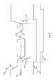
- a timing diagram 600 shows an example of an assertion of the erasure flag beginning shortly before the location where the media defect is identified and extending until shortly after the media defect is identified.
- Timing diagram 600 shows an example waveform of a combined correlation value 605 in relation to an ideal erasure flag 650 and a delayed erasure flag 670 .
- ideal erasure flag 650 is asserted at a point 637 a predetermined period 635 prior to a point 615 where combined correlation value 605 drops below threshold 610 .
- a delayed erasure flag 670 is generated that is delayed by a period 680 .
- period 680 is greater than or equal to period 635 .
- Period 680 is implemented by delay circuit 322 of FIG. 3 that was described above.
- Ideal erasure flag 650 is de-asserted at a point 647 a predetermined period 640 after a point 630 where combined correlation value 605 exceeds threshold 610 .
- delayed erasure flag 670 is de-asserted at a point delayed by period 680 .
- delay erasure flag 670 there is no transition of delay erasure flag 670 corresponding to the transitions of combined correlation value 605 passing through threshold value 610 at points 620 , 625 . This occurs because the time during which combined correlation value 605 exceeds threshold value 610 is less than period 635 plus period 640 .
- Such integrated circuits may include all of the functions of a given block, system or circuit, or only a subset of the block, system or circuit. Further, elements of the blocks, systems or circuits may be implemented across multiple integrated circuits. Such integrated circuits may be any type of integrated circuit known in the art including, but are not limited to, a monolithic integrated circuit, a flip chip integrated circuit, a multichip module integrated circuit, and/or a mixed signal integrated circuit. It should also be noted that various functions of the blocks, systems or circuits discussed herein may be implemented in either software or firmware. In some such cases, the entire system, block or circuit may be implemented using its software or firmware equivalent. In other cases, the one part of a given system, block or circuit may be implemented in software or firmware, while other parts are implemented in hardware.
- the invention provides novel systems, devices, methods and arrangements for performing defect detection. While detailed descriptions of one or more embodiments of the invention have been given above, various alternatives, modifications, and equivalents will be apparent to those skilled in the art without varying from the spirit of the invention. For example, one or more embodiments of the present invention may be applied to various data storage systems and digital communication systems, such as, for example, tape recording systems, optical disk drives, wireless systems, and digital subscriber line systems. Therefore, the above description should not be taken as limiting the scope of the invention, which is defined by the appended claims.
Abstract
Description
Extrinsic Output=Intrinsic Output−a priori value,
as is known in the art.
| If ([Decoder | ||
| | |
| |
| { |
| |
| } | |
| Else | |
| { |
| |
| } | ||
A moving
Extrinsic Output=Intrinsic Output−a priori value,
as is known in the art.
Extrinsic Output=Intrinsic Output−a priori value,
as is known in the art.
| If ([Decoder Soft Output * Extrinsic Soft Output] > 0 && | ||
| Extrinsic Soft Output > 10 && | |
| Decoder Soft Output > 10) |
| { |
| Pre-compensated Data = Extrinsic Soft Output |
| } | |
| Else | |
| { |
| Pre-compensated Data = 2* Decoder Soft Output |
| } | ||
A moving average of the pre-compensated data is calculated to yield a first moving average (block 508). In some embodiments of the present invention, the moving average is an average of the sixteen most recent values of pre-compensated data. The first moving average is subtracted from the most current pre-compensated data to yield a first sum (block 512).
Correlation=[(The Fourth Moving Average)/(The First Square Root)]/(The Second Square Root).
Correlation=[(The Second Moving Average)/(The Second Square Root)]/(The First Square Root).
Claims (20)
Priority Applications (1)
| Application Number | Priority Date | Filing Date | Title |
|---|---|---|---|
| US13/088,119 US8887034B2 (en) | 2011-04-15 | 2011-04-15 | Systems and methods for short media defect detection |
Applications Claiming Priority (1)
| Application Number | Priority Date | Filing Date | Title |
|---|---|---|---|
| US13/088,119 US8887034B2 (en) | 2011-04-15 | 2011-04-15 | Systems and methods for short media defect detection |
Publications (2)
| Publication Number | Publication Date |
|---|---|
| US20120266055A1 US20120266055A1 (en) | 2012-10-18 |
| US8887034B2 true US8887034B2 (en) | 2014-11-11 |
Family
ID=47007323
Family Applications (1)
| Application Number | Title | Priority Date | Filing Date |
|---|---|---|---|
| US13/088,119 Active 2032-07-31 US8887034B2 (en) | 2011-04-15 | 2011-04-15 | Systems and methods for short media defect detection |
Country Status (1)
| Country | Link |
|---|---|
| US (1) | US8887034B2 (en) |
Families Citing this family (14)
| Publication number | Priority date | Publication date | Assignee | Title |
|---|---|---|---|---|
| US8949701B2 (en) | 2008-09-23 | 2015-02-03 | Agere Systems Inc. | Systems and methods for low latency media defect detection |
| US9129653B2 (en) | 2012-04-20 | 2015-09-08 | Avago Technologies General Ip (Singapore) Pte. Ltd. | Systems and methods for calibration coasting in a data processing system |
| US8819521B2 (en) | 2012-04-30 | 2014-08-26 | Lsi Corporation | Systems and methods for short media defect detection using non-binary coded information |
| US8675297B2 (en) | 2012-06-15 | 2014-03-18 | Lsi Corporation | Media defect classification |
| US9076492B2 (en) | 2012-07-12 | 2015-07-07 | Lsi Corporation | Systems and methods for rapid erasure retry decoding |
| US8826110B2 (en) | 2012-07-17 | 2014-09-02 | Lsi Corporation | Systems and methods for defect scanning |
| US8732562B2 (en) | 2012-07-25 | 2014-05-20 | Lsi Corporation | Systems and methods for improved short media defect detection |
| US8972800B2 (en) | 2012-07-30 | 2015-03-03 | Lsi Corporation | Systems and methods for enhanced media defect detection |
| US9245586B2 (en) | 2012-10-18 | 2016-01-26 | Avago Technologies General Ip (Singapore) Pte. Ltd. | Systems and methods for short media defect detection using multi-iteration soft data feedback |
| US8996970B2 (en) | 2012-10-24 | 2015-03-31 | Lsi Corporation | Systems and methods for positive feedback short media defect detection |
| US9244752B2 (en) | 2013-05-02 | 2016-01-26 | Avago Technologies General Ip (Singapore) Pte. Ltd. | Systems and methods for detecting media flaws |
| US8917468B1 (en) | 2013-06-06 | 2014-12-23 | Lsi Corporation | Systems and methods for media defect detection with pattern qualification |
| JP7377637B2 (en) * | 2019-06-28 | 2023-11-10 | 三菱重工業株式会社 | Abnormality detection device, abnormality detection method, and program |
| US11757459B2 (en) * | 2022-02-17 | 2023-09-12 | Caelus Technologies Limited | Cascode Class-A differential reference buffer using source followers for a multi-channel interleaved Analog-to-Digital Converter (ADC) |
Citations (136)
| Publication number | Priority date | Publication date | Assignee | Title |
|---|---|---|---|---|
| EP0522578A2 (en) | 1991-07-12 | 1993-01-13 | Pioneer Electronic Corporation | Noise removing circuit |
| US5278846A (en) | 1990-06-11 | 1994-01-11 | Matsushita Electric Industrial Co., Ltd. | Digital signal decoder |
| US5278703A (en) | 1991-06-21 | 1994-01-11 | Digital Equipment Corp. | Embedded servo banded format for magnetic disks for use with a data processing system |
| US5325402A (en) | 1991-04-30 | 1994-06-28 | Nec Corporation | Method and arrangement for estimating data sequences transmsitted using Viterbi algorithm |
| US5392299A (en) | 1992-01-15 | 1995-02-21 | E-Systems, Inc. | Triple orthogonally interleaed error correction system |
| EP0631277A3 (en) | 1993-06-22 | 1995-02-22 | Quantum Corp | ID-less data sector format and data controller for disk drive. |
| US5471500A (en) | 1994-03-08 | 1995-11-28 | At&T Ipm Corp. | Soft symbol decoding |
| US5513192A (en) | 1992-08-28 | 1996-04-30 | Sun Microsystems, Inc. | Fault tolerant disk drive system with error detection and correction |
| US5523903A (en) | 1993-12-23 | 1996-06-04 | International Business Machines Corporation | Sector architecture for fixed block disk drive |
| US5550870A (en) | 1994-03-02 | 1996-08-27 | Lucent Technologies Inc. | Viterbi processor |
| US5612964A (en) | 1991-04-08 | 1997-03-18 | Haraszti; Tegze P. | High performance, fault tolerant orthogonal shuffle memory and method |
| US5701314A (en) | 1995-12-21 | 1997-12-23 | Cirrus Logic, Inc. | On-the-fly error correction using thermal asperity erasure pointers from a sampled amplitude read channel in a magnetic disk drive |
| US5710784A (en) | 1993-09-24 | 1998-01-20 | Qualcomm Incorporated | Multirate serial viterbi decoder for code division multiple access system applications |
| US5712861A (en) | 1994-07-12 | 1998-01-27 | Mitsubishi Denki Kabushiki Kaisha | Error correcting method and decoder with improved reliability |
| US5717706A (en) | 1994-03-04 | 1998-02-10 | Sony Corporation | Apparatus and method for detecting signal points using signal point-mapping |
| US5802118A (en) | 1996-07-29 | 1998-09-01 | Cirrus Logic, Inc. | Sub-sampled discrete time read channel for computer storage systems |
| US5844945A (en) | 1994-04-12 | 1998-12-01 | Goldstar Co., Ltd. | Viterbi decoder for a high definition television |
| US5898710A (en) | 1995-06-06 | 1999-04-27 | Globespan Technologies, Inc. | Implied interleaving, a family of systematic interleavers and deinterleavers |
| US5923713A (en) | 1996-02-28 | 1999-07-13 | Sony Corporation | Viterbi decoder |
| US5978414A (en) | 1996-07-03 | 1999-11-02 | Matsushita Electric Industrial Co., Ltd. | Transmission rate judging unit |
| US5983383A (en) | 1997-01-17 | 1999-11-09 | Qualcom Incorporated | Method and apparatus for transmitting and receiving concatenated code data |
| US6005897A (en) | 1997-12-16 | 1999-12-21 | Mccallister; Ronald D. | Data communication system and method therefor |
| US6023783A (en) | 1996-05-15 | 2000-02-08 | California Institute Of Technology | Hybrid concatenated codes and iterative decoding |
| US6029264A (en) | 1997-04-28 | 2000-02-22 | The Trustees Of Princeton University | System and method for error correcting a received data stream in a concatenated system |
| US6065149A (en) | 1996-11-21 | 2000-05-16 | Matsushita Electric Industrial Co., Ltd. | Error correction device for a communication system |
| US6145110A (en) | 1998-06-22 | 2000-11-07 | Ericsson Inc. | Digital data decoder that derives codeword estimates from soft data |
| US6216251B1 (en) | 1999-04-30 | 2001-04-10 | Motorola Inc | On-chip error detection and correction system for an embedded non-volatile memory array and method of operation |
| US6216249B1 (en) | 1999-03-03 | 2001-04-10 | Cirrus Logic, Inc. | Simplified branch metric for reducing the cost of a trellis sequence detector in a sampled amplitude read channel |
| US6229467B1 (en) | 1999-05-28 | 2001-05-08 | Telefonaktiebolaget Lm Ericsson (Publ) | Correction static errors in a/d-converter |
| US6266795B1 (en) | 1999-05-28 | 2001-07-24 | Lucent Technologies Inc. | Turbo code termination |
| US6317472B1 (en) | 1997-08-07 | 2001-11-13 | Samsung Electronics Co., Ltd. | Viterbi decoder |
| US6351832B1 (en) | 1999-05-28 | 2002-02-26 | Lucent Technologies Inc. | Turbo code symbol interleaver |
| US6377610B1 (en) | 1997-04-25 | 2002-04-23 | Deutsche Telekom Ag | Decoding method and decoding device for a CDMA transmission system for demodulating a received signal available in serial code concatenation |
| US6381726B1 (en) | 1999-01-04 | 2002-04-30 | Maxtor Corporation | Architecture for soft decision decoding of linear block error correcting codes |
| US6438717B1 (en) | 1999-05-26 | 2002-08-20 | 3Com Corporation | High speed parallel bit error rate tester |
| US6473878B1 (en) | 1999-05-28 | 2002-10-29 | Lucent Technologies Inc. | Serial-concatenated turbo codes |
| US6476989B1 (en) | 1996-07-09 | 2002-11-05 | International Business Machines Corporation | Radial self-propagation pattern generation for disk file servowriting |
| US20030063405A1 (en) | 2001-10-02 | 2003-04-03 | Ming Jin | Method and apparatus for detecting media defects |
| US20030066020A1 (en) * | 2001-06-11 | 2003-04-03 | Fujitsu Limited | Recording and reproducing apparatus, signal decoding circuit, error correction method and iterative decoder |
| US20030081693A1 (en) | 2001-07-11 | 2003-05-01 | Raghavan Sreen A. | Low complexity high-speed communications transceiver |
| US20030087634A1 (en) | 2001-07-11 | 2003-05-08 | Raghavan Sreen A. | 10165368High-speed multi-channel communications transceiver with inter-channel interference filter |
| US20030112896A1 (en) | 2001-07-11 | 2003-06-19 | Raghavan Sreen A. | Multi-channel communications transceiver |
| US6625775B1 (en) | 1998-12-10 | 2003-09-23 | Samsung Electronics Co., Ltd. | Encoder/decoder with serial concatenated structure in communication system |
| US6657803B1 (en) | 1999-11-22 | 2003-12-02 | Seagate Technology Llc | Method and apparatus for data error recovery using defect threshold detector and viterbi gain |
| US6671404B1 (en) | 1997-02-14 | 2003-12-30 | Hewlett-Packard Development Company, L.P. | Method and apparatus for recognizing patterns |
| US20040071206A1 (en) | 2002-08-13 | 2004-04-15 | Fujitsu Limited. | Digital filter adaptively learning filter coefficient |
| US20040098659A1 (en) | 2002-11-18 | 2004-05-20 | Bjerke Bjorn A. | Rate-compatible LDPC codes |
| US6748034B2 (en) | 1997-12-19 | 2004-06-08 | Sony Corporation | Viterbi decoding apparatus and viterbi decoding method |
| US6757862B1 (en) | 2000-08-21 | 2004-06-29 | Handspring, Inc. | Method and apparatus for digital data error correction coding |
| US6785863B2 (en) | 2002-09-18 | 2004-08-31 | Motorola, Inc. | Method and apparatus for generating parity-check bits from a symbol set |
| US6788654B1 (en) | 1998-01-29 | 2004-09-07 | Nippon Hoso Kyokai | Digital data receiver |
| US6810502B2 (en) | 2000-01-28 | 2004-10-26 | Conexant Systems, Inc. | Iteractive decoder employing multiple external code error checks to lower the error floor |
| US20050010855A1 (en) | 2003-07-09 | 2005-01-13 | Itay Lusky | Reduced complexity decoding for trellis coded modulation |
| US20050078399A1 (en) | 2003-10-10 | 2005-04-14 | Seagate Technology Llc | Using data compression to achieve lower linear bit densities on a storage medium |
| US20050111540A1 (en) | 2001-11-21 | 2005-05-26 | David Modrie | Adaptive equalizer operating at a sampling rate asynchronous to the data rate |
| US20050157780A1 (en) | 2003-12-17 | 2005-07-21 | Werner Carl W. | Signaling system with selectively-inhibited adaptive equalization |
| US20050195749A1 (en) | 2004-03-05 | 2005-09-08 | Elmasry George F. | Method and system for capacity analysis for On The Move adhoc wireless packet-switched networks |
| US20050216819A1 (en) | 2004-02-19 | 2005-09-29 | Trellisware Technologies, Inc. | Method and apparatus for communications using turbo like codes |
| US20050273688A1 (en) | 2004-06-02 | 2005-12-08 | Cenk Argon | Data communication system with multi-dimensional error-correction product codes |
| US6980382B2 (en) | 2001-11-09 | 2005-12-27 | Fujitsu Limited | Magnetic disk drive system |
| US6986098B2 (en) | 2001-11-20 | 2006-01-10 | Lsi Logic Corporation | Method of reducing miscorrections in a post-processor using column parity checks |
| US20060020872A1 (en) | 2004-07-21 | 2006-01-26 | Tom Richardson | LDPC encoding methods and apparatus |
| US20060031737A1 (en) | 2004-02-19 | 2006-02-09 | Trellisware Technologies, Inc. | Method and apparatus for communications using improved turbo like codes |
| WO2006016751A2 (en) | 2004-08-09 | 2006-02-16 | Lg Electronics Inc. | Method of encoding and decoding using low density parity check matrix |
| US7010051B2 (en) | 2000-03-24 | 2006-03-07 | Sony Corporation | Coding apparatus, coding method and recording medium having coded program recorded therein, and decoding apparatus, decoding method and recording medium having decoded program recorded therein |
| US7047474B2 (en) | 2002-12-23 | 2006-05-16 | Do-Jun Rhee | Decoding concatenated codes via parity bit recycling |
| US7058873B2 (en) | 2002-11-07 | 2006-06-06 | Carnegie Mellon University | Encoding method using a low density parity check code with a column weight of two |
| US20060123285A1 (en) | 2004-11-16 | 2006-06-08 | De Araujo Daniel F | Dynamic threshold scaling in a communication system |
| US20060140311A1 (en) | 2004-12-23 | 2006-06-29 | Agere Systems Inc. | Composite data detector and a method for detecting data |
| US7073118B2 (en) | 2001-09-17 | 2006-07-04 | Digeo, Inc. | Apparatus and method for saturating decoder values |
| US20060168493A1 (en) | 2005-01-24 | 2006-07-27 | Agere Systems Inc. | Data detection and decoding system and method |
| US7093179B2 (en) | 2001-03-22 | 2006-08-15 | University Of Florida | Method and coding means for error-correction utilizing concatenated parity and turbo codes |
| US20060195772A1 (en) | 2005-02-28 | 2006-08-31 | Nils Graef | Method and apparatus for evaluating performance of a read channel |
| US20060210002A1 (en) | 2005-03-03 | 2006-09-21 | Xueshi Yang | Timing recovery in a parallel channel communication system |
| US7113356B1 (en) | 2002-09-10 | 2006-09-26 | Marvell International Ltd. | Method for checking the quality of servo gray codes |
| US20060248435A1 (en) | 2005-04-29 | 2006-11-02 | Haratsch Erich F | Method and apparatus for iterative error-erasure decoding |
| US7136244B1 (en) | 2002-02-22 | 2006-11-14 | Western Digital Technologies, Inc. | Disk drive employing data averaging techniques during retry operations to facilitate data recovery |
| US20060256670A1 (en) | 2005-05-16 | 2006-11-16 | Samsung Electronics Co., Ltd. | Signal-to-noise ratio measurement apparatus and method for signal read out of optical disc |
| WO2006134527A1 (en) | 2005-06-16 | 2006-12-21 | Koninklijke Philips Electronics N.V. | Ofdm receiver with csi based llr metrics |
| US20070011569A1 (en) | 2005-06-20 | 2007-01-11 | The Regents Of The University Of California | Variable-rate low-density parity check codes with constant blocklength |
| US7173783B1 (en) | 2001-09-21 | 2007-02-06 | Maxtor Corporation | Media noise optimized detector for magnetic recording |
| US7184486B1 (en) | 2000-04-27 | 2007-02-27 | Marvell International Ltd. | LDPC encoder and decoder and method thereof |
| US20070047635A1 (en) | 2005-08-24 | 2007-03-01 | Stojanovic Vladimir M | Signaling system with data correlation detection |
| US20070047121A1 (en) | 2005-08-26 | 2007-03-01 | Eleftheriou Evangelos S | Read channel apparatus for asynchronous sampling and synchronous equalization |
| US7191378B2 (en) | 2002-07-03 | 2007-03-13 | The Directv Group, Inc. | Method and system for providing low density parity check (LDPC) encoding |
| US7203015B2 (en) | 2003-07-31 | 2007-04-10 | Kabushiki Kaisha Toshiba | Method and apparatus for decoding sync marks in a disk |
| US20070110200A1 (en) | 2005-11-15 | 2007-05-17 | Gokhan Mergen | Equalizer for a receiver in a wireless communication system |
| US20070162838A1 (en) * | 2005-09-22 | 2007-07-12 | Atsushi Esumi | Data writing apparatus and a storage system |
| US7257764B2 (en) | 2003-11-03 | 2007-08-14 | Broadcom Corporation | FEC (Forward Error Correction) decoder with dynamic parameters |
| WO2007091797A2 (en) | 2006-02-08 | 2007-08-16 | Lg Electronics Inc. | Method of matching codeword size and transmitter therefor in mobile communications system |
| US20070230407A1 (en) | 2006-03-31 | 2007-10-04 | Petrie Michael C | Dynamic, adaptive power control for a half-duplex wireless communication system |
| US20070286270A1 (en) | 2001-09-05 | 2007-12-13 | Mediatek Inc. | Read channel apparatus and method for an optical storage system |
| US7313750B1 (en) | 2003-08-06 | 2007-12-25 | Ralink Technology, Inc. | Efficient soft decision demapper to minimize viterbi decoder complexity |
| US20080043356A1 (en) * | 2006-08-18 | 2008-02-21 | Seagate Technology Llc | Read error recovery using soft information |
| US20080049825A1 (en) | 2006-08-25 | 2008-02-28 | Broadcom Corporation | Equalizer with reorder |
| US20080055122A1 (en) | 2006-07-31 | 2008-03-06 | Agere Systems Inc. | Systems and Methods for Code Based Error Reduction |
| US20080065970A1 (en) | 2006-07-31 | 2008-03-13 | Agere Systems Inc. | Systems and Methods for Code Dependency Reduction |
| US20080069373A1 (en) | 2006-09-20 | 2008-03-20 | Broadcom Corporation | Low frequency noise reduction circuit architecture for communications applications |
| US20080104486A1 (en) * | 2006-10-31 | 2008-05-01 | Fujitsu Limited | Decoder and reproducing device |
| US7370258B2 (en) | 2005-04-28 | 2008-05-06 | Sandbridge Technologies Inc. | Iterative concatenated convolutional Reed-Solomon decoding method |
| US20080168330A1 (en) | 2007-01-08 | 2008-07-10 | Agere Systems Inc. | Systems and methods for prioritizing error correction data |
| US7430256B2 (en) | 2003-09-26 | 2008-09-30 | Samsung Electronics Co., Ltd. | Method and apparatus for providing channel state information |
| US20080276156A1 (en) | 2007-05-01 | 2008-11-06 | Texas A&M University System | Low density parity check decoder for regular ldpc codes |
| EP1814108B1 (en) | 2005-09-12 | 2008-11-26 | Sony Corporation | Noise reducing apparatus, method and program and sound pickup apparatus for electronic equipment |
| US7502189B2 (en) | 2000-10-23 | 2009-03-10 | Hitachi Global Storage Technologies Japan, Ltd. | Apparatus, signal-processing circuit and device for magnetic recording system |
| US7505537B1 (en) | 2003-03-25 | 2009-03-17 | Marvell International Ltd. | System and method for controlling gain and timing phase in a presence of a first least mean square filter using a second adaptive filter |
| US7523375B2 (en) | 2005-09-21 | 2009-04-21 | Distribution Control Systems | Set of irregular LDPC codes with random structure and low encoding complexity |
| US20090185643A1 (en) | 2008-01-22 | 2009-07-23 | Fitzpatrick Kelly K | Methods and Apparatus for Map Detection with Reduced Complexity |
| US20090199073A1 (en) * | 2008-01-31 | 2009-08-06 | Fujitsu Limited | Encoding device, decoding device, encoding/decoding device, and recording/reproducing device |
| US20090199071A1 (en) | 2008-02-05 | 2009-08-06 | Agere Systems Inc. | Systems and Methods for Low Cost LDPC Decoding |
| US7590927B1 (en) | 2005-11-14 | 2009-09-15 | Link —A—Media Devices Corporation | Soft output viterbi detector with error event output |
| US20090235116A1 (en) * | 2008-03-17 | 2009-09-17 | Agere Systems Inc. | Systems and Methods for Regenerating Data from a Defective Medium |
| US20090235146A1 (en) * | 2008-03-17 | 2009-09-17 | Agere Systems Inc. | Systems and Methods for Using Intrinsic Data for Regenerating Data from a Defective Medium |
| US20090259915A1 (en) | 2004-10-12 | 2009-10-15 | Michael Livshitz | Structured low-density parity-check (ldpc) code |
| US20090268848A1 (en) * | 2008-04-29 | 2009-10-29 | Agere Systems Inc. | Systems and Methods for Filter Based Media Defect Detection |
| US20090271670A1 (en) * | 2008-04-29 | 2009-10-29 | Agere Systems Inc. | Systems and Methods for Media Defect Detection Utilizing Correlated DFIR and LLR Data |
| US20090273492A1 (en) | 2008-05-02 | 2009-11-05 | Lsi Corporation | Systems and Methods for Queue Based Data Detection and Decoding |
| US20090274247A1 (en) | 2008-04-30 | 2009-11-05 | Richard Leo Galbraith | Detection of synchronization mark from output of matched filter upstream of viterbi detector |
| US20100042877A1 (en) * | 2007-10-01 | 2010-02-18 | Weijun Tan | Systems and Methods for Media Defect Detection |
| US20100042890A1 (en) | 2008-08-15 | 2010-02-18 | Lsi Corporation | Error-floor mitigation of ldpc codes using targeted bit adjustments |
| US20100050043A1 (en) | 2006-12-01 | 2010-02-25 | Commissariat A L'energie Atomique | Method and device for decoding ldpc codes and communication apparatus including such device |
| US20100061492A1 (en) | 2008-09-05 | 2010-03-11 | Lsi Corporation | Reduced Frequency Data Processing Using a Matched Filter Set Front End |
| US20100070837A1 (en) | 2008-09-17 | 2010-03-18 | LSI Corporatrion | Power Reduced Queue Based Data Detection and Decoding Systems and Methods for Using Such |
| US7702989B2 (en) | 2006-09-27 | 2010-04-20 | Agere Systems Inc. | Systems and methods for generating erasure flags |
| US7712008B2 (en) | 2006-01-26 | 2010-05-04 | Agere Systems Inc. | Systems and methods for error reduction associated with information transfer |
| US20100164764A1 (en) | 2008-05-19 | 2010-07-01 | Ratnakar Aravind Nayak | Systems and Methods for Mitigating Latency in a Data Detector Feedback Loop |
| US7752523B1 (en) | 2006-02-13 | 2010-07-06 | Marvell International Ltd. | Reduced-complexity decoding of parity check codes |
| US20100185914A1 (en) | 2007-09-28 | 2010-07-22 | Weijun Tan | Systems and Methods for Reduced Complexity Data Processing |
| US20100226033A1 (en) * | 2009-03-06 | 2010-09-09 | Agere Systems Inc. | Systems and Methods for Enhanced Media Defect Detection |
| WO2010101578A1 (en) | 2009-03-05 | 2010-09-10 | Lsi Corporation | Improved turbo-equalization methods for iterative decoders |
| US20100269023A1 (en) * | 2009-04-17 | 2010-10-21 | Agere Systems Inc. | Systems and Methods for Multilevel Media Defect Detection |
| WO2010126482A1 (en) | 2009-04-28 | 2010-11-04 | Lsi Corporation | Systems and methods for dynamic scaling in a read data processing system |
| US20110075569A1 (en) | 2008-04-18 | 2011-03-31 | Link_A_Media Devices Corporation | Obtaining parameters for minimizing an error event probability |
| US20110080211A1 (en) | 2008-11-20 | 2011-04-07 | Shaohua Yang | Systems and Methods for Noise Reduced Data Detection |
| US20110167246A1 (en) | 2010-01-04 | 2011-07-07 | Lsi Corporation | Systems and Methods for Data Detection Including Dynamic Scaling |
| US20120047396A1 (en) * | 2010-08-20 | 2012-02-23 | Stmicroelectronics, Inc. | Identifying a defect in a data-storage medium |
-
2011
- 2011-04-15 US US13/088,119 patent/US8887034B2/en active Active
Patent Citations (151)
| Publication number | Priority date | Publication date | Assignee | Title |
|---|---|---|---|---|
| US5278846A (en) | 1990-06-11 | 1994-01-11 | Matsushita Electric Industrial Co., Ltd. | Digital signal decoder |
| US5612964A (en) | 1991-04-08 | 1997-03-18 | Haraszti; Tegze P. | High performance, fault tolerant orthogonal shuffle memory and method |
| US5325402A (en) | 1991-04-30 | 1994-06-28 | Nec Corporation | Method and arrangement for estimating data sequences transmsitted using Viterbi algorithm |
| US5278703A (en) | 1991-06-21 | 1994-01-11 | Digital Equipment Corp. | Embedded servo banded format for magnetic disks for use with a data processing system |
| EP0522578A2 (en) | 1991-07-12 | 1993-01-13 | Pioneer Electronic Corporation | Noise removing circuit |
| US5392299A (en) | 1992-01-15 | 1995-02-21 | E-Systems, Inc. | Triple orthogonally interleaed error correction system |
| US5513192A (en) | 1992-08-28 | 1996-04-30 | Sun Microsystems, Inc. | Fault tolerant disk drive system with error detection and correction |
| EP0631277A3 (en) | 1993-06-22 | 1995-02-22 | Quantum Corp | ID-less data sector format and data controller for disk drive. |
| US5710784A (en) | 1993-09-24 | 1998-01-20 | Qualcomm Incorporated | Multirate serial viterbi decoder for code division multiple access system applications |
| US5523903A (en) | 1993-12-23 | 1996-06-04 | International Business Machines Corporation | Sector architecture for fixed block disk drive |
| US5768044A (en) | 1993-12-23 | 1998-06-16 | International Business Machines Corporation | Zoned recording embedded servo disk drive having no data identification fields and reduced rotational latency |
| US5550870A (en) | 1994-03-02 | 1996-08-27 | Lucent Technologies Inc. | Viterbi processor |
| US5717706A (en) | 1994-03-04 | 1998-02-10 | Sony Corporation | Apparatus and method for detecting signal points using signal point-mapping |
| US6041432A (en) | 1994-03-04 | 2000-03-21 | Sony Corporation | Apparatus and method for detecting signal points using signal point-mapping |
| US5471500A (en) | 1994-03-08 | 1995-11-28 | At&T Ipm Corp. | Soft symbol decoding |
| US5844945A (en) | 1994-04-12 | 1998-12-01 | Goldstar Co., Ltd. | Viterbi decoder for a high definition television |
| US5712861A (en) | 1994-07-12 | 1998-01-27 | Mitsubishi Denki Kabushiki Kaisha | Error correcting method and decoder with improved reliability |
| US5898710A (en) | 1995-06-06 | 1999-04-27 | Globespan Technologies, Inc. | Implied interleaving, a family of systematic interleavers and deinterleavers |
| US5701314A (en) | 1995-12-21 | 1997-12-23 | Cirrus Logic, Inc. | On-the-fly error correction using thermal asperity erasure pointers from a sampled amplitude read channel in a magnetic disk drive |
| US5923713A (en) | 1996-02-28 | 1999-07-13 | Sony Corporation | Viterbi decoder |
| US6023783A (en) | 1996-05-15 | 2000-02-08 | California Institute Of Technology | Hybrid concatenated codes and iterative decoding |
| US5978414A (en) | 1996-07-03 | 1999-11-02 | Matsushita Electric Industrial Co., Ltd. | Transmission rate judging unit |
| US6476989B1 (en) | 1996-07-09 | 2002-11-05 | International Business Machines Corporation | Radial self-propagation pattern generation for disk file servowriting |
| US5802118A (en) | 1996-07-29 | 1998-09-01 | Cirrus Logic, Inc. | Sub-sampled discrete time read channel for computer storage systems |
| US6065149A (en) | 1996-11-21 | 2000-05-16 | Matsushita Electric Industrial Co., Ltd. | Error correction device for a communication system |
| US5983383A (en) | 1997-01-17 | 1999-11-09 | Qualcom Incorporated | Method and apparatus for transmitting and receiving concatenated code data |
| US6671404B1 (en) | 1997-02-14 | 2003-12-30 | Hewlett-Packard Development Company, L.P. | Method and apparatus for recognizing patterns |
| US6377610B1 (en) | 1997-04-25 | 2002-04-23 | Deutsche Telekom Ag | Decoding method and decoding device for a CDMA transmission system for demodulating a received signal available in serial code concatenation |
| US6029264A (en) | 1997-04-28 | 2000-02-22 | The Trustees Of Princeton University | System and method for error correcting a received data stream in a concatenated system |
| US6317472B1 (en) | 1997-08-07 | 2001-11-13 | Samsung Electronics Co., Ltd. | Viterbi decoder |
| US6097764A (en) | 1997-12-16 | 2000-08-01 | Sicom, Inc. | Pragmatic trellis-coded modulation system and method therefor |
| US6005897A (en) | 1997-12-16 | 1999-12-21 | Mccallister; Ronald D. | Data communication system and method therefor |
| US6748034B2 (en) | 1997-12-19 | 2004-06-08 | Sony Corporation | Viterbi decoding apparatus and viterbi decoding method |
| US6788654B1 (en) | 1998-01-29 | 2004-09-07 | Nippon Hoso Kyokai | Digital data receiver |
| US6145110A (en) | 1998-06-22 | 2000-11-07 | Ericsson Inc. | Digital data decoder that derives codeword estimates from soft data |
| US6625775B1 (en) | 1998-12-10 | 2003-09-23 | Samsung Electronics Co., Ltd. | Encoder/decoder with serial concatenated structure in communication system |
| US6381726B1 (en) | 1999-01-04 | 2002-04-30 | Maxtor Corporation | Architecture for soft decision decoding of linear block error correcting codes |
| US6216249B1 (en) | 1999-03-03 | 2001-04-10 | Cirrus Logic, Inc. | Simplified branch metric for reducing the cost of a trellis sequence detector in a sampled amplitude read channel |
| US6216251B1 (en) | 1999-04-30 | 2001-04-10 | Motorola Inc | On-chip error detection and correction system for an embedded non-volatile memory array and method of operation |
| US6438717B1 (en) | 1999-05-26 | 2002-08-20 | 3Com Corporation | High speed parallel bit error rate tester |
| US6229467B1 (en) | 1999-05-28 | 2001-05-08 | Telefonaktiebolaget Lm Ericsson (Publ) | Correction static errors in a/d-converter |
| US6266795B1 (en) | 1999-05-28 | 2001-07-24 | Lucent Technologies Inc. | Turbo code termination |
| US6351832B1 (en) | 1999-05-28 | 2002-02-26 | Lucent Technologies Inc. | Turbo code symbol interleaver |
| US6473878B1 (en) | 1999-05-28 | 2002-10-29 | Lucent Technologies Inc. | Serial-concatenated turbo codes |
| US6657803B1 (en) | 1999-11-22 | 2003-12-02 | Seagate Technology Llc | Method and apparatus for data error recovery using defect threshold detector and viterbi gain |
| US7310768B2 (en) | 2000-01-28 | 2007-12-18 | Conexant Systems, Inc. | Iterative decoder employing multiple external code error checks to lower the error floor |
| US6810502B2 (en) | 2000-01-28 | 2004-10-26 | Conexant Systems, Inc. | Iteractive decoder employing multiple external code error checks to lower the error floor |
| US7010051B2 (en) | 2000-03-24 | 2006-03-07 | Sony Corporation | Coding apparatus, coding method and recording medium having coded program recorded therein, and decoding apparatus, decoding method and recording medium having decoded program recorded therein |
| US7184486B1 (en) | 2000-04-27 | 2007-02-27 | Marvell International Ltd. | LDPC encoder and decoder and method thereof |
| US6757862B1 (en) | 2000-08-21 | 2004-06-29 | Handspring, Inc. | Method and apparatus for digital data error correction coding |
| US7502189B2 (en) | 2000-10-23 | 2009-03-10 | Hitachi Global Storage Technologies Japan, Ltd. | Apparatus, signal-processing circuit and device for magnetic recording system |
| US7093179B2 (en) | 2001-03-22 | 2006-08-15 | University Of Florida | Method and coding means for error-correction utilizing concatenated parity and turbo codes |
| US20030066020A1 (en) * | 2001-06-11 | 2003-04-03 | Fujitsu Limited | Recording and reproducing apparatus, signal decoding circuit, error correction method and iterative decoder |
| US20030112896A1 (en) | 2001-07-11 | 2003-06-19 | Raghavan Sreen A. | Multi-channel communications transceiver |
| US7403752B2 (en) | 2001-07-11 | 2008-07-22 | Vativ Technologies, Inc. | Multi-channel communications transceiver |
| US7590168B2 (en) | 2001-07-11 | 2009-09-15 | Entropic Communications, Inc. | Low complexity high-speed communications transceiver |
| US20030134607A1 (en) | 2001-07-11 | 2003-07-17 | Raghavan Sreeen A. | Multi-channel communications transceiver |
| US7236757B2 (en) | 2001-07-11 | 2007-06-26 | Vativ Technologies, Inc. | High-speed multi-channel communications transceiver with inter-channel interference filter |
| US20030087634A1 (en) | 2001-07-11 | 2003-05-08 | Raghavan Sreen A. | 10165368High-speed multi-channel communications transceiver with inter-channel interference filter |
| US20030081693A1 (en) | 2001-07-11 | 2003-05-01 | Raghavan Sreen A. | Low complexity high-speed communications transceiver |
| US20100002795A1 (en) | 2001-07-11 | 2010-01-07 | Entropic Communications, Inc. | Low Complexity High-Speed Communications Transceiver |
| US20070286270A1 (en) | 2001-09-05 | 2007-12-13 | Mediatek Inc. | Read channel apparatus and method for an optical storage system |
| US7073118B2 (en) | 2001-09-17 | 2006-07-04 | Digeo, Inc. | Apparatus and method for saturating decoder values |
| US7173783B1 (en) | 2001-09-21 | 2007-02-06 | Maxtor Corporation | Media noise optimized detector for magnetic recording |
| US20030063405A1 (en) | 2001-10-02 | 2003-04-03 | Ming Jin | Method and apparatus for detecting media defects |
| US6980382B2 (en) | 2001-11-09 | 2005-12-27 | Fujitsu Limited | Magnetic disk drive system |
| US6986098B2 (en) | 2001-11-20 | 2006-01-10 | Lsi Logic Corporation | Method of reducing miscorrections in a post-processor using column parity checks |
| US20050111540A1 (en) | 2001-11-21 | 2005-05-26 | David Modrie | Adaptive equalizer operating at a sampling rate asynchronous to the data rate |
| US7136244B1 (en) | 2002-02-22 | 2006-11-14 | Western Digital Technologies, Inc. | Disk drive employing data averaging techniques during retry operations to facilitate data recovery |
| US7203887B2 (en) | 2002-07-03 | 2007-04-10 | The Directtv Group, Inc. | Method and system for routing in low density parity check (LDPC) decoders |
| US7191378B2 (en) | 2002-07-03 | 2007-03-13 | The Directv Group, Inc. | Method and system for providing low density parity check (LDPC) encoding |
| US20040071206A1 (en) | 2002-08-13 | 2004-04-15 | Fujitsu Limited. | Digital filter adaptively learning filter coefficient |
| US7113356B1 (en) | 2002-09-10 | 2006-09-26 | Marvell International Ltd. | Method for checking the quality of servo gray codes |
| US6785863B2 (en) | 2002-09-18 | 2004-08-31 | Motorola, Inc. | Method and apparatus for generating parity-check bits from a symbol set |
| US7058873B2 (en) | 2002-11-07 | 2006-06-06 | Carnegie Mellon University | Encoding method using a low density parity check code with a column weight of two |
| US20040098659A1 (en) | 2002-11-18 | 2004-05-20 | Bjerke Bjorn A. | Rate-compatible LDPC codes |
| US7047474B2 (en) | 2002-12-23 | 2006-05-16 | Do-Jun Rhee | Decoding concatenated codes via parity bit recycling |
| US7505537B1 (en) | 2003-03-25 | 2009-03-17 | Marvell International Ltd. | System and method for controlling gain and timing phase in a presence of a first least mean square filter using a second adaptive filter |
| US20050010855A1 (en) | 2003-07-09 | 2005-01-13 | Itay Lusky | Reduced complexity decoding for trellis coded modulation |
| US7203015B2 (en) | 2003-07-31 | 2007-04-10 | Kabushiki Kaisha Toshiba | Method and apparatus for decoding sync marks in a disk |
| US7313750B1 (en) | 2003-08-06 | 2007-12-25 | Ralink Technology, Inc. | Efficient soft decision demapper to minimize viterbi decoder complexity |
| US7430256B2 (en) | 2003-09-26 | 2008-09-30 | Samsung Electronics Co., Ltd. | Method and apparatus for providing channel state information |
| US20050078399A1 (en) | 2003-10-10 | 2005-04-14 | Seagate Technology Llc | Using data compression to achieve lower linear bit densities on a storage medium |
| US7257764B2 (en) | 2003-11-03 | 2007-08-14 | Broadcom Corporation | FEC (Forward Error Correction) decoder with dynamic parameters |
| US20050157780A1 (en) | 2003-12-17 | 2005-07-21 | Werner Carl W. | Signaling system with selectively-inhibited adaptive equalization |
| US20060031737A1 (en) | 2004-02-19 | 2006-02-09 | Trellisware Technologies, Inc. | Method and apparatus for communications using improved turbo like codes |
| US20050216819A1 (en) | 2004-02-19 | 2005-09-29 | Trellisware Technologies, Inc. | Method and apparatus for communications using turbo like codes |
| US20050195749A1 (en) | 2004-03-05 | 2005-09-08 | Elmasry George F. | Method and system for capacity analysis for On The Move adhoc wireless packet-switched networks |
| US20050273688A1 (en) | 2004-06-02 | 2005-12-08 | Cenk Argon | Data communication system with multi-dimensional error-correction product codes |
| US20060020872A1 (en) | 2004-07-21 | 2006-01-26 | Tom Richardson | LDPC encoding methods and apparatus |
| WO2006016751A2 (en) | 2004-08-09 | 2006-02-16 | Lg Electronics Inc. | Method of encoding and decoding using low density parity check matrix |
| US20090259915A1 (en) | 2004-10-12 | 2009-10-15 | Michael Livshitz | Structured low-density parity-check (ldpc) code |
| US20060123285A1 (en) | 2004-11-16 | 2006-06-08 | De Araujo Daniel F | Dynamic threshold scaling in a communication system |
| US20060140311A1 (en) | 2004-12-23 | 2006-06-29 | Agere Systems Inc. | Composite data detector and a method for detecting data |
| US20060168493A1 (en) | 2005-01-24 | 2006-07-27 | Agere Systems Inc. | Data detection and decoding system and method |
| US20060195772A1 (en) | 2005-02-28 | 2006-08-31 | Nils Graef | Method and apparatus for evaluating performance of a read channel |
| US20060210002A1 (en) | 2005-03-03 | 2006-09-21 | Xueshi Yang | Timing recovery in a parallel channel communication system |
| US7370258B2 (en) | 2005-04-28 | 2008-05-06 | Sandbridge Technologies Inc. | Iterative concatenated convolutional Reed-Solomon decoding method |
| US20060248435A1 (en) | 2005-04-29 | 2006-11-02 | Haratsch Erich F | Method and apparatus for iterative error-erasure decoding |
| US7587657B2 (en) | 2005-04-29 | 2009-09-08 | Agere Systems Inc. | Method and apparatus for iterative error-erasure decoding |
| US20060256670A1 (en) | 2005-05-16 | 2006-11-16 | Samsung Electronics Co., Ltd. | Signal-to-noise ratio measurement apparatus and method for signal read out of optical disc |
| WO2006134527A1 (en) | 2005-06-16 | 2006-12-21 | Koninklijke Philips Electronics N.V. | Ofdm receiver with csi based llr metrics |
| US20070011569A1 (en) | 2005-06-20 | 2007-01-11 | The Regents Of The University Of California | Variable-rate low-density parity check codes with constant blocklength |
| US20070047635A1 (en) | 2005-08-24 | 2007-03-01 | Stojanovic Vladimir M | Signaling system with data correlation detection |
| US20070047121A1 (en) | 2005-08-26 | 2007-03-01 | Eleftheriou Evangelos S | Read channel apparatus for asynchronous sampling and synchronous equalization |
| EP1814108B1 (en) | 2005-09-12 | 2008-11-26 | Sony Corporation | Noise reducing apparatus, method and program and sound pickup apparatus for electronic equipment |
| US7523375B2 (en) | 2005-09-21 | 2009-04-21 | Distribution Control Systems | Set of irregular LDPC codes with random structure and low encoding complexity |
| US20070162838A1 (en) * | 2005-09-22 | 2007-07-12 | Atsushi Esumi | Data writing apparatus and a storage system |
| US7590927B1 (en) | 2005-11-14 | 2009-09-15 | Link —A—Media Devices Corporation | Soft output viterbi detector with error event output |
| US20070110200A1 (en) | 2005-11-15 | 2007-05-17 | Gokhan Mergen | Equalizer for a receiver in a wireless communication system |
| US7712008B2 (en) | 2006-01-26 | 2010-05-04 | Agere Systems Inc. | Systems and methods for error reduction associated with information transfer |
| WO2007091797A2 (en) | 2006-02-08 | 2007-08-16 | Lg Electronics Inc. | Method of matching codeword size and transmitter therefor in mobile communications system |
| US7752523B1 (en) | 2006-02-13 | 2010-07-06 | Marvell International Ltd. | Reduced-complexity decoding of parity check codes |
| US20070230407A1 (en) | 2006-03-31 | 2007-10-04 | Petrie Michael C | Dynamic, adaptive power control for a half-duplex wireless communication system |
| US7802163B2 (en) | 2006-07-31 | 2010-09-21 | Agere Systems Inc. | Systems and methods for code based error reduction |
| US7801200B2 (en) | 2006-07-31 | 2010-09-21 | Agere Systems Inc. | Systems and methods for code dependency reduction |
| US20080065970A1 (en) | 2006-07-31 | 2008-03-13 | Agere Systems Inc. | Systems and Methods for Code Dependency Reduction |
| US20080055122A1 (en) | 2006-07-31 | 2008-03-06 | Agere Systems Inc. | Systems and Methods for Code Based Error Reduction |
| US7738201B2 (en) | 2006-08-18 | 2010-06-15 | Seagate Technology Llc | Read error recovery using soft information |
| US20080043356A1 (en) * | 2006-08-18 | 2008-02-21 | Seagate Technology Llc | Read error recovery using soft information |
| US20080049825A1 (en) | 2006-08-25 | 2008-02-28 | Broadcom Corporation | Equalizer with reorder |
| US20080069373A1 (en) | 2006-09-20 | 2008-03-20 | Broadcom Corporation | Low frequency noise reduction circuit architecture for communications applications |
| US7702989B2 (en) | 2006-09-27 | 2010-04-20 | Agere Systems Inc. | Systems and methods for generating erasure flags |
| US20080104486A1 (en) * | 2006-10-31 | 2008-05-01 | Fujitsu Limited | Decoder and reproducing device |
| US20100050043A1 (en) | 2006-12-01 | 2010-02-25 | Commissariat A L'energie Atomique | Method and device for decoding ldpc codes and communication apparatus including such device |
| US20080168330A1 (en) | 2007-01-08 | 2008-07-10 | Agere Systems Inc. | Systems and methods for prioritizing error correction data |
| US20080276156A1 (en) | 2007-05-01 | 2008-11-06 | Texas A&M University System | Low density parity check decoder for regular ldpc codes |
| US20080301521A1 (en) | 2007-05-01 | 2008-12-04 | Texas A&M University System | Low density parity check decoder for irregular ldpc codes |
| US20100185914A1 (en) | 2007-09-28 | 2010-07-22 | Weijun Tan | Systems and Methods for Reduced Complexity Data Processing |
| US20100042877A1 (en) * | 2007-10-01 | 2010-02-18 | Weijun Tan | Systems and Methods for Media Defect Detection |
| US20090185643A1 (en) | 2008-01-22 | 2009-07-23 | Fitzpatrick Kelly K | Methods and Apparatus for Map Detection with Reduced Complexity |
| US20090199073A1 (en) * | 2008-01-31 | 2009-08-06 | Fujitsu Limited | Encoding device, decoding device, encoding/decoding device, and recording/reproducing device |
| US20090199071A1 (en) | 2008-02-05 | 2009-08-06 | Agere Systems Inc. | Systems and Methods for Low Cost LDPC Decoding |
| US20090235116A1 (en) * | 2008-03-17 | 2009-09-17 | Agere Systems Inc. | Systems and Methods for Regenerating Data from a Defective Medium |
| US20090235146A1 (en) * | 2008-03-17 | 2009-09-17 | Agere Systems Inc. | Systems and Methods for Using Intrinsic Data for Regenerating Data from a Defective Medium |
| US20110075569A1 (en) | 2008-04-18 | 2011-03-31 | Link_A_Media Devices Corporation | Obtaining parameters for minimizing an error event probability |
| US20090268848A1 (en) * | 2008-04-29 | 2009-10-29 | Agere Systems Inc. | Systems and Methods for Filter Based Media Defect Detection |
| US20090271670A1 (en) * | 2008-04-29 | 2009-10-29 | Agere Systems Inc. | Systems and Methods for Media Defect Detection Utilizing Correlated DFIR and LLR Data |
| US20090274247A1 (en) | 2008-04-30 | 2009-11-05 | Richard Leo Galbraith | Detection of synchronization mark from output of matched filter upstream of viterbi detector |
| US20090273492A1 (en) | 2008-05-02 | 2009-11-05 | Lsi Corporation | Systems and Methods for Queue Based Data Detection and Decoding |
| US20100164764A1 (en) | 2008-05-19 | 2010-07-01 | Ratnakar Aravind Nayak | Systems and Methods for Mitigating Latency in a Data Detector Feedback Loop |
| US20100042890A1 (en) | 2008-08-15 | 2010-02-18 | Lsi Corporation | Error-floor mitigation of ldpc codes using targeted bit adjustments |
| US20100061492A1 (en) | 2008-09-05 | 2010-03-11 | Lsi Corporation | Reduced Frequency Data Processing Using a Matched Filter Set Front End |
| US20100070837A1 (en) | 2008-09-17 | 2010-03-18 | LSI Corporatrion | Power Reduced Queue Based Data Detection and Decoding Systems and Methods for Using Such |
| US20110080211A1 (en) | 2008-11-20 | 2011-04-07 | Shaohua Yang | Systems and Methods for Noise Reduced Data Detection |
| WO2010101578A1 (en) | 2009-03-05 | 2010-09-10 | Lsi Corporation | Improved turbo-equalization methods for iterative decoders |
| US20100226033A1 (en) * | 2009-03-06 | 2010-09-09 | Agere Systems Inc. | Systems and Methods for Enhanced Media Defect Detection |
| US20100269023A1 (en) * | 2009-04-17 | 2010-10-21 | Agere Systems Inc. | Systems and Methods for Multilevel Media Defect Detection |
| WO2010126482A1 (en) | 2009-04-28 | 2010-11-04 | Lsi Corporation | Systems and methods for dynamic scaling in a read data processing system |
| US20110167246A1 (en) | 2010-01-04 | 2011-07-07 | Lsi Corporation | Systems and Methods for Data Detection Including Dynamic Scaling |
| US20120047396A1 (en) * | 2010-08-20 | 2012-02-23 | Stmicroelectronics, Inc. | Identifying a defect in a data-storage medium |
Non-Patent Citations (92)
| Title |
|---|
| Amer et al "Design Issues for a Shingled Write Disk System" MSST IEEE 26th Symposium May 2010. |
| Bahl, et al "Optimal decoding of linear codes for Minimizing symbol error rate", IEEE Trans. Inform. Theory, vol. 20, pp. 284-287, Mar. 1974. |
| Casado et al., Multiple-rate low-denstiy parity-check codes with constant blocklength, IEEE Transations on communications, Jan. 2009, vol. 57, pp. 75-83. |
| Collins and Hizlan, "Determinate State Convolutional Codes" IEEE Transactions on Communications, Dec. 1993. |
| Eleftheriou, E. et al., "Low Density Parity-Check Codes for Digital Subscriber Lines", Proc ICC 2002, pp. 1752-1757. |
| Fisher, R et al., "Adaptive Thresholding"[online] 2003 [retrieved on May 28, 2010] Retrieved from the Internet <URL:http://homepages.inf.ed.ac.uk/rbf/HIPR2/adpthrsh.htm. |
| Fossnorier, Marc P.C. "Quasi-Cyclic Low-Density Parity-Check Codes From Circulant Permutation Maricies" IEEE Transactions on Information Theory, vol. 50, No. 8 Aug. 8, 2004. |
| Gibson et al "Directions for Shingled-Write and Two-Dimensional Magnetic Recording System" Architectures: Synergies with Solid-State Disks Carnegie Mellon Univ. May 1, 2009. |
| Hagenauer, J. et al A Viterbi Algorithm with Soft-Decision Outputs and its Applications in Proc. IEEE Globecom, pp. 47. 11-47 Dallas, TX Nov. 1989. |
| Han and Ryan, "Pinning Techniques for Low-Floor Detection/Decoding of LDPC-Coded Partial Response Channels", 5th International Symposium on Turbo Codes &Related Topics, 2008. |
| K. Gunnam "Area and Energy Efficient VLSI Architectures for Low-Density Parity-Check Decoders Using an On-The-Fly Computation" dissertation at Texas A&M University, Dec. 2006. |
| K. Gunnam et al., "Next Generation iterative LDPC solutions for magnetic recording storage", invited paper. The Asilomar Conference on Signals, Systems, and Computers, Nov. 2008. |
| K. Gunnam et al., "Value-Reuse Properties of Min-Sum for GF(q)" (dated Oct. 2006) Dept. of ECE, Texas A&M University Technical Note, published about Aug. 2010. |
| K. Gunnam et al., "Value-Reuse Properties of Min-Sum for GF(q)"(dated Jul. 2008) Dept. of ECE, Texas A&M University Technical Note, published about Aug. 2010. |
| Landini G, "Auto threshold and Auto Local Threshold" [online] [retrieved May 28, 2010] Retrieved from the Internet: <URL:http://www.dentistry.bham.ac.uk/landinig/software/autothreshold/autoreshold.html. |
| Lee et al., "Partial Zero-Forcing Adaptive MMSE Receiver for DS-CDMA Uplink in Multicell Environments" IEEE Transactions on Vehicular Tech. vol. 51, No. 5, Sep. 2002. |
| Lin et al "An efficient VLSI Architecture for non binary LDPC decoders"-IEEE Transaction on Circuits and Systems II vol. 57, Issue 1 (Jan. 2010) pp. 51-55. |
| Lin et al "An efficient VLSI Architecture for non binary LDPC decoders"—IEEE Transaction on Circuits and Systems II vol. 57, Issue 1 (Jan. 2010) pp. 51-55. |
| Mohsenin et al., "Split Row: A Reduced Complexity, High Throughput LDPC Decoder Architecture", pp. 1-6, printed from www.ece.ucdavis.edu on Jul. 9, 2007. |
| Moon et al, "Pattern-dependent noise prediction in signal-dependent Noise," IEEE JSAC, vol. 19, No. 4 pp. 730-743, Apr. 2001. |
| Perisa et al "Frequency Offset Estimation Based on Phase Offsets Between Sample Correlations" Dept. of Info. Tech. University of Ulm 2005. |
| Sari H et al., "Transmission Techniques for Digital Terrestrial TV Broadcasting" IEEE Communications Magazine, IEEE Service Center Ny, NY vol. 33, No. 2 Feb. 1995. |
| Selvarathinam, A.: "Low Density Parity-Check Decoder Architecture for High Throughput Optical Fiber Channels" IEEE International Conference on Computer Design (ICCD '03) 2003. |
| Shu Lin, Ryan, "Channel Codes, Classical and Modern" 2009, Cambridge University Press, pp. 213-222. |
| U.S. Appl. No. 11/461,026, filed Jul. 31, 2006, Tan, Weijun. |
| U.S. Appl. No. 11/461,198, filed Jul. 31, 2006, Tan, Weijun. |
| U.S. Appl. No. 11/461,283, filed Jul. 31, 2006, Tan, Weijun. |
| U.S. Appl. No. 12/540,283, filed Aug. 12, 2009, Liu, et al. |
| U.S. Appl. No. 12/652,201, filed Jan. 5, 2010, Mathew, et al. |
| U.S. Appl. No. 12/763,050, filed Apr. 19, 2010, Ivkovic, et al. |
| U.S. Appl. No. 12/792,555, filed Jun. 2, 2010, Liu, et al. |
| U.S. Appl. No. 12/887,317, filed Sep. 21, 2010, Xia, et al. |
| U.S. Appl. No. 12/887,330, filed Sep. 21, 2010, Zhang, et al. |
| U.S. Appl. No. 12/887,369, filed Sep. 21, 2010, Liu, et al. |
| U.S. Appl. No. 12/901,742, filed Oct. 11, 2010, Yang. |
| U.S. Appl. No. 12/901,816, filed Oct. 11, 2010, Li, et al. |
| U.S. Appl. No. 12/917,756, filed Nov. 2, 2010, Miladinovic, et al. |
| U.S. Appl. No. 12/947,931, filed Nov. 17, 2010, Yang, Shaohua. |
| U.S. Appl. No. 12/947,947, filed Nov. 17, 2010, Ivkovic, et al. |
| U.S. Appl. No. 12/972,942, filed Dec. 20, 2010, Liao, et al. |
| U.S. Appl. No. 12/992,948, filed Nov. 16, 2010, Yang, et al. |
| U.S. Appl. No. 13/021,814, filed Feb. 7, 2011, Jin, Ming, et al. |
| U.S. Appl. No. 13/031,818, filed Feb. 22, 2011, Xu, Changyou, et al. |
| U.S. Appl. No. 13/050,129, filed Mar. 17, 2011, Tan, et al. |
| U.S. Appl. No. 13/050,765, filed Mar. 17, 2011, Yang, et al. |
| U.S. Appl. No. 13/088,119, filed Apr. 15, 2011, Zhang, et al. |
| U.S. Appl. No. 13/088,146, filed Apr. 15, 2011, Li, et al. |
| U.S. Appl. No. 13/088,178, filed Apr. 15, 2011, Sun, et al. |
| U.S. Appl. No. 13/126,748, filed Apr. 28, 2011, Tan. |
| U.S. Appl. No. 13/167,764, filed Jun. 24, 2011, Li, Zongwang, et al. |
| U.S. Appl. No. 13/167,771, filed Jun. 24, 2011, Li, Zongwang, et al. |
| U.S. Appl. No. 13/167,775, filed Jun. 24, 2011, Li, Zongwang. |
| U.S. Appl. No. 13/186,146, filed Jul. 19, 2011, Mathew, et al. |
| U.S. Appl. No. 13/186,174, filed Jul. 19, 2011, Mathew, et al. |
| U.S. Appl. No. 13/186,197, filed Jul. 19, 2011, Mathew, George et al. |
| U.S. Appl. No. 13/186,213, filed Jul. 19, 2011, Mathew, et al. |
| U.S. Appl. No. 13/186,234, filed Jul. 19, 2011, Xia, Haitao, et al. |
| U.S. Appl. No. 13/186,251, filed Jul. 19, 2011, Xia, Haitao, et al. |
| U.S. Appl. No. 13/213,751, filed Aug. 19, 2011, Zhang, Fan, et al. |
| U.S. Appl. No. 13/213,808, filed Aug. 19, 2011, Jin, Ming. |
| U.S. Appl. No. 13/220,142, filed Aug. 29, 2011, Chang, Wu, et al. |
| U.S. Appl. No. 13/227,538, filed Sep. 8, 2011, Yang, Shaohua, et al. |
| U.S. Appl. No. 13/227,544, filed Sep. 8, 2011, Yang, Shaohua, et al. |
| U.S. Appl. No. 13/239,683, filed Sep. 22, 2011, Xu, Changyou. |
| U.S. Appl. No. 13/239,719, filed Sep. 22, 2011, Xia, Haitao, et al. |
| U.S. Appl. No. 13/251,340, filed Oct. 3, 2011, Xia, Haitao, et al. |
| U.S. Appl. No. 13/251,342, filed Oct. 2, 2011, Xia, Haitao, et al. |
| U.S. Appl. No. 13/269,832, filed Oct. 10, 2011, Xia, Haitao, et al. |
| U.S. Appl. No. 13/269,852, filed Oct. 10, 2011, Xia, Haitao, et al. |
| U.S. Appl. No. 13/284,730, filed Oct. 28, 2011, Zhang, Fan, et al. |
| U.S. Appl. No. 13/284,754, filed Oct. 28, 2011, Zhang, Fan, et al. |
| U.S. Appl. No. 13/284,767, filed Oct. 28, 2011, Zhang, Fan, et al. |
| U.S. Appl. No. 13/284,819, filed Oct. 28, 2011, Tan, Weijun, et al. |
| U.S. Appl. No. 13/284,826, filed Oct. 28, 2011, Tan, Weijun, et al. |
| U.S. Appl. No. 13/295,150, filed Nov. 14, 2011, Li, Zongwang, et al. |
| U.S. Appl. No. 13/295,160, filed Nov. 14, 2011, Li, Zongwang, et al. |
| Vasic, B., "High-Rate Girth-Eight Codes on Rectangular Integer Lattices", IEEE Trans. Communications, vol. 52, Aug. 2004, pp. 1248-1252. |
| Vasic, B., "High-Rate Low-Density Parity-Check Codes Based on Anti-Pasch Affine Geometries," Proc ICC 2002, pp. 1332-1336. |
| Wang Y et al., "A Soft Decision Decoding Scheme for Wireless COFDM With Application to DVB-T" IEEE Trans. on Consumer elec., IEEE Service Center, NY,NY vo. 50, No. 1 Feb. 2004. |
| Weon-Cheol Lee et al., "Vitierbi Decoding Method Using Channel State Info. in COFDM System" IEEE Trans. on Consumer Elect., IEEE Service Center, NY, NY vol. 45, No. 3 Aug. 1999. |
| Xia et al, "A Chase-GMD algorithm of Reed-Solomon codes on perpendicular channels", IEEE Transactions on Magnetics, vol. 42 pp. 2603-2605, Oct. 2006. |
| Xia et al, "Reliability-based Reed-Solomon decoding for magnetic recording channels", IEEE International Conference on Communication pp. 1977-1981, May 2008. |
| Yeo et al., "VLSI Architecture for Iterative Decoders in Magnetic Storage Channels", Mar. 2001, pp. 748-755, IEEE trans. Magnetics, vol. 37, No. 2. |
| Youn, et al. "BER Perform. Due to Irrreg. of Row-Weight Distrib. of the Parity-Chk. Matirx in Irreg. LDPC Codes for 10-Gb/s Opt. Signls" Jrnl of Lightwave Tech., vol. 23, Sep. 2005. |
| Zhong et al., "Area-Efficient Min-Sum Decoder VLSI Architecture for High-Rate QC-LDPC Codes in Magnetic Recording", pp. 1-15, Submitted 2006, not yet published. |
| Zhong et al., "Design of VLSI Implementation-Oriented LDPC Codes", IEEE, pp. 670-673, 2003. |
| Zhong et al., "High-Rate Quasi-Cyclic LDPC Codes for Magnetic Recording Channel with Low Error Floor", ISCAS, IEEE pp. 3546-3549, May 2006. |
| Zhong et al., "Iterative MAX-LOG-MAP and LDPC Detector/Decoder Hardware Implementation for Magnetic Read Channel", SRC Techron, pp. 1-4, Oct. 2005. |
| Zhong et al., "Joint Code-Encoder Design for LDPC Coding System VLSI Implementation", ISCAS, IEEE pp. 389-392, May 2004. |
| Zhong et al., "Quasi Cyclic LDPC Codes for the Magnetic Recording Channel: Code Design and VSLI Implementation", IEEE Transactions on Magnetics, v. 43, pp. 1118-1123, Mar. 2007. |
| Zhong, "Block-LDPC: A Practical LDPC Coding System Design Approach", IEEE Trans. on Circuits, Regular Papers, vol. 5, No. 4, pp. 766-775, Apr. 2005. |
| Zhong, "VLSI Architecture of LDPC Based Signal Detection and Coding System for Magnetic Recording Channel", Thesis, RPI, Troy, NY, pp. 1-95, May 2006. |
Also Published As
| Publication number | Publication date |
|---|---|
| US20120266055A1 (en) | 2012-10-18 |
Similar Documents
| Publication | Publication Date | Title |
|---|---|---|
| US8887034B2 (en) | Systems and methods for short media defect detection | |
| US8670955B2 (en) | Systems and methods for reliability assisted noise predictive filtering | |
| US8295001B2 (en) | Systems and methods for low latency noise cancellation | |
| US8611033B2 (en) | Systems and methods for selective decoder input data processing | |
| US8810940B2 (en) | Systems and methods for off track error recovery | |
| US8139457B2 (en) | Systems and methods for low latency media defect detection | |
| US8843813B2 (en) | Systems and methods for media defect detection | |
| US8667039B2 (en) | Systems and methods for variance dependent normalization for branch metric calculation | |
| US8121224B2 (en) | Systems and methods for filter based media defect detection | |
| US8411537B2 (en) | Systems and methods for recovering information from a defective medium | |
| US8854753B2 (en) | Systems and methods for auto scaling in a data processing system | |
| US8261171B2 (en) | Systems and methods for diversity combined data detection | |
| US8614858B2 (en) | Systems and methods for sync mark detection metric computation | |
| US8750447B2 (en) | Systems and methods for variable thresholding in a pattern detector | |
| US8566379B2 (en) | Systems and methods for self tuning target adaptation | |
| US8745439B2 (en) | Systems and methods for multilevel media defect detection | |
| US8862972B2 (en) | Low latency multi-detector noise cancellation | |
| US20120236428A1 (en) | Systems and Methods for Sync Mark Detection | |
| US8762440B2 (en) | Systems and methods for area efficient noise predictive filter calibration | |
| US8838660B2 (en) | Systems and methods for reducing filter sensitivities | |
| US8665544B2 (en) | Systems and methods for servo data detection | |
| US8760991B2 (en) | Systems and methods for post processing gain correction | |
| US8949701B2 (en) | Systems and methods for low latency media defect detection |
Legal Events
| Date | Code | Title | Description |
|---|---|---|---|
| AS | Assignment |
Owner name: LSI CORPORATION, CALIFORNIA Free format text: ASSIGNMENT OF ASSIGNORS INTEREST;ASSIGNORS:ZHANG, FAN;YANG, SHAOHUA;REEL/FRAME:026137/0849 Effective date: 20110411 |
|
| STCF | Information on status: patent grant |
Free format text: PATENTED CASE |
|
| AS | Assignment |
Owner name: AVAGO TECHNOLOGIES GENERAL IP (SINGAPORE) PTE. LTD Free format text: ASSIGNMENT OF ASSIGNORS INTEREST;ASSIGNOR:LSI CORPORATION;REEL/FRAME:035390/0388 Effective date: 20140814 |
|
| AS | Assignment |
Owner name: BANK OF AMERICA, N.A., AS COLLATERAL AGENT, NORTH CAROLINA Free format text: PATENT SECURITY AGREEMENT;ASSIGNOR:AVAGO TECHNOLOGIES GENERAL IP (SINGAPORE) PTE. LTD.;REEL/FRAME:037808/0001 Effective date: 20160201 Owner name: BANK OF AMERICA, N.A., AS COLLATERAL AGENT, NORTH Free format text: PATENT SECURITY AGREEMENT;ASSIGNOR:AVAGO TECHNOLOGIES GENERAL IP (SINGAPORE) PTE. LTD.;REEL/FRAME:037808/0001 Effective date: 20160201 |
|
| AS | Assignment |
Owner name: AVAGO TECHNOLOGIES GENERAL IP (SINGAPORE) PTE. LTD., SINGAPORE Free format text: TERMINATION AND RELEASE OF SECURITY INTEREST IN PATENTS;ASSIGNOR:BANK OF AMERICA, N.A., AS COLLATERAL AGENT;REEL/FRAME:041710/0001 Effective date: 20170119 Owner name: AVAGO TECHNOLOGIES GENERAL IP (SINGAPORE) PTE. LTD Free format text: TERMINATION AND RELEASE OF SECURITY INTEREST IN PATENTS;ASSIGNOR:BANK OF AMERICA, N.A., AS COLLATERAL AGENT;REEL/FRAME:041710/0001 Effective date: 20170119 |
|
| MAFP | Maintenance fee payment |
Free format text: PAYMENT OF MAINTENANCE FEE, 4TH YEAR, LARGE ENTITY (ORIGINAL EVENT CODE: M1551) Year of fee payment: 4 |
|
| AS | Assignment |
Owner name: AVAGO TECHNOLOGIES INTERNATIONAL SALES PTE. LIMITE Free format text: MERGER;ASSIGNOR:AVAGO TECHNOLOGIES GENERAL IP (SINGAPORE) PTE. LTD.;REEL/FRAME:047229/0408 Effective date: 20180509 |
|
| AS | Assignment |
Owner name: AVAGO TECHNOLOGIES INTERNATIONAL SALES PTE. LIMITE Free format text: CORRECTIVE ASSIGNMENT TO CORRECT THE EFFECTIVE DATE PREVIOUSLY RECORDED ON REEL 047229 FRAME 0408. ASSIGNOR(S) HEREBY CONFIRMS THE THE EFFECTIVE DATE IS 09/05/2018;ASSIGNOR:AVAGO TECHNOLOGIES GENERAL IP (SINGAPORE) PTE. LTD.;REEL/FRAME:047349/0001 Effective date: 20180905 |
|
| AS | Assignment |
Owner name: AVAGO TECHNOLOGIES INTERNATIONAL SALES PTE. LIMITE Free format text: CORRECTIVE ASSIGNMENT TO CORRECT THE PATENT NUMBER 9,385,856 TO 9,385,756 PREVIOUSLY RECORDED AT REEL: 47349 FRAME: 001. ASSIGNOR(S) HEREBY CONFIRMS THE MERGER;ASSIGNOR:AVAGO TECHNOLOGIES GENERAL IP (SINGAPORE) PTE. LTD.;REEL/FRAME:051144/0648 Effective date: 20180905 |
|
| MAFP | Maintenance fee payment |
Free format text: PAYMENT OF MAINTENANCE FEE, 8TH YEAR, LARGE ENTITY (ORIGINAL EVENT CODE: M1552); ENTITY STATUS OF PATENT OWNER: LARGE ENTITY Year of fee payment: 8 |