US8873615B2 - Method and controller for equalizing a received serial data stream - Google Patents
Method and controller for equalizing a received serial data stream Download PDFInfo
- Publication number
- US8873615B2 US8873615B2 US13/622,508 US201213622508A US8873615B2 US 8873615 B2 US8873615 B2 US 8873615B2 US 201213622508 A US201213622508 A US 201213622508A US 8873615 B2 US8873615 B2 US 8873615B2
- Authority
- US
- United States
- Prior art keywords
- tap
- taps
- signal
- controller
- compensation circuit
- Prior art date
- Legal status (The legal status is an assumption and is not a legal conclusion. Google has not performed a legal analysis and makes no representation as to the accuracy of the status listed.)
- Active, expires
Links
- 238000000034 method Methods 0.000 title claims abstract description 36
- 239000006185 dispersion Substances 0.000 claims abstract description 64
- 238000004891 communication Methods 0.000 claims abstract description 24
- 230000004044 response Effects 0.000 claims abstract description 5
- 239000002243 precursor Substances 0.000 claims description 18
- 230000003044 adaptive effect Effects 0.000 claims description 2
- 238000010586 diagram Methods 0.000 description 32
- 230000003287 optical effect Effects 0.000 description 15
- 230000009467 reduction Effects 0.000 description 11
- 230000001934 delay Effects 0.000 description 10
- 230000003111 delayed effect Effects 0.000 description 9
- 239000000835 fiber Substances 0.000 description 9
- 238000013459 approach Methods 0.000 description 8
- 230000005540 biological transmission Effects 0.000 description 3
- 230000000694 effects Effects 0.000 description 3
- 230000001771 impaired effect Effects 0.000 description 3
- 238000000926 separation method Methods 0.000 description 3
- 238000004088 simulation Methods 0.000 description 3
- 238000007796 conventional method Methods 0.000 description 2
- 230000006735 deficit Effects 0.000 description 2
- 238000004519 manufacturing process Methods 0.000 description 2
- 230000004048 modification Effects 0.000 description 2
- 238000012986 modification Methods 0.000 description 2
- 238000005457 optimization Methods 0.000 description 2
- 238000005070 sampling Methods 0.000 description 2
- 230000035945 sensitivity Effects 0.000 description 2
- 230000008054 signal transmission Effects 0.000 description 2
- RYGMFSIKBFXOCR-UHFFFAOYSA-N Copper Chemical compound [Cu] RYGMFSIKBFXOCR-UHFFFAOYSA-N 0.000 description 1
- 239000000654 additive Substances 0.000 description 1
- 230000000996 additive effect Effects 0.000 description 1
- 230000002411 adverse Effects 0.000 description 1
- 239000003990 capacitor Substances 0.000 description 1
- 230000015556 catabolic process Effects 0.000 description 1
- 230000008859 change Effects 0.000 description 1
- 229910052802 copper Inorganic materials 0.000 description 1
- 239000010949 copper Substances 0.000 description 1
- 238000012937 correction Methods 0.000 description 1
- 238000006731 degradation reaction Methods 0.000 description 1
- 238000001514 detection method Methods 0.000 description 1
- 238000005259 measurement Methods 0.000 description 1
- 230000007246 mechanism Effects 0.000 description 1
- 238000012544 monitoring process Methods 0.000 description 1
- 238000010606 normalization Methods 0.000 description 1
- 238000012545 processing Methods 0.000 description 1
- 238000011084 recovery Methods 0.000 description 1
- 230000004043 responsiveness Effects 0.000 description 1
- 238000001228 spectrum Methods 0.000 description 1
- 230000007704 transition Effects 0.000 description 1
Images


Classifications
-
- H—ELECTRICITY
- H04—ELECTRIC COMMUNICATION TECHNIQUE
- H04L—TRANSMISSION OF DIGITAL INFORMATION, e.g. TELEGRAPHIC COMMUNICATION
- H04L25/00—Baseband systems
- H04L25/02—Details ; arrangements for supplying electrical power along data transmission lines
- H04L25/03—Shaping networks in transmitter or receiver, e.g. adaptive shaping networks
- H04L25/03006—Arrangements for removing intersymbol interference
- H04L25/03012—Arrangements for removing intersymbol interference operating in the time domain
- H04L25/03019—Arrangements for removing intersymbol interference operating in the time domain adaptive, i.e. capable of adjustment during data reception
- H04L25/03038—Arrangements for removing intersymbol interference operating in the time domain adaptive, i.e. capable of adjustment during data reception with a non-recursive structure
- H04L25/03044—Arrangements for removing intersymbol interference operating in the time domain adaptive, i.e. capable of adjustment during data reception with a non-recursive structure using fractionally spaced delay lines or combinations of fractionally integrally spaced taps
-
- H—ELECTRICITY
- H04—ELECTRIC COMMUNICATION TECHNIQUE
- H04L—TRANSMISSION OF DIGITAL INFORMATION, e.g. TELEGRAPHIC COMMUNICATION
- H04L25/00—Baseband systems
- H04L25/02—Details ; arrangements for supplying electrical power along data transmission lines
- H04L25/03—Shaping networks in transmitter or receiver, e.g. adaptive shaping networks
- H04L25/03006—Arrangements for removing intersymbol interference
- H04L2025/0335—Arrangements for removing intersymbol interference characterised by the type of transmission
- H04L2025/03356—Baseband transmission
-
- H—ELECTRICITY
- H04—ELECTRIC COMMUNICATION TECHNIQUE
- H04L—TRANSMISSION OF DIGITAL INFORMATION, e.g. TELEGRAPHIC COMMUNICATION
- H04L25/00—Baseband systems
- H04L25/02—Details ; arrangements for supplying electrical power along data transmission lines
- H04L25/03—Shaping networks in transmitter or receiver, e.g. adaptive shaping networks
- H04L25/03006—Arrangements for removing intersymbol interference
- H04L2025/03592—Adaptation methods
Definitions
- the invention relates to communications networks over which data is serially communicated in the form of time-varying signals transmitted and received over various data transmission media.
- Digital communication receivers sample an incoming waveform and then reliably detect the sampled data.
- a receiver includes a Clock and Data Recovery (CDR) system to recover the clock and data from an incoming data stream.
- CDR Clock and Data Recovery
- the CDR system generates a clock signal having the same frequency and phase as the incoming signal, which is then used to sample the received signal and detect the transmitted data.
- the quality of the received signal is often impaired by inter-symbol interference, crosstalk, echo, and other noise.
- impairments in the receiver itself may further degrade the quality of the received signal.
- the received signal can be viewed as a well-known “data eye,” which is a superposition of a number of impaired individual signals with varying frequency components, for example, due to ISI and other noise. As the various impairments increase, the quality of an eye diagram or eye trace derived from or otherwise detected by observation of the received signal is impaired.
- An eye diagram corresponds to a superposition of samples of a serial data signal over a unit interval of the data signal (i.e., the shortest time period over which the data signal can change state).
- An eye diagram may be generated by applying the serial data signal to the vertical input of an oscilloscope and triggering a horizontal sweep across the unit interval based on the data rate of the serial data signal.
- the superposed samples appear on the oscilloscope display as an eye diagram with an eye opening bounded by two transition regions.
- Various features of the eye opening reveal information about the quality of the communications channel over which the serial data signal is transmitted. For example, a wide eye opening indicates that the serial data signal has a relatively low noise level and a relatively low bit-error rate, whereas a narrow eye opening indicates that the serial data signal has a relatively high noise level and a relatively high bit-error rate.
- Eye margining is a technique by which the height and width, or margins, of a data eye can be measured.
- the eye margin of a receiver can be evaluated following the manufacturing process, or prior to deployment in a given application, to determine if the receiver satisfies one or more predefined margin criteria. If the receiver does not satisfy the one or more predefined margin criteria, the device can be rejected or one or more device parameters can be modified and the margin criteria can be reevaluated. Eye margining is often performed using a classical jitter tolerance technique and eye histogram techniques.
- An eye diagram typically is evaluated based on the width of the eye opening, the height of the eye opening, and the rate of closure of the eye opening with variation of the sampling time.
- the width of the eye opening corresponds to the time interval over which the serial data signal can be sampled without inter-symbol interference.
- the height of the eye opening corresponds to a measure of the signal-to-noise ratio of the serial data signal.
- the rate of closure of the eye opening with variation of the sampling time indicates the sensitivity of the serial data signal to timing errors.
- Various eye margining or monitoring circuits have been developed that measure one or more characteristic features of an eye diagram of a serial data signal in real-time.
- the measured features typically are used to correct distortions that are introduced into the serial data signal by the communication channel.
- the frequency responses of some adaptive equalizers are optimized based on measurements of signal quality as indicated by one or more characteristic eye diagram features.
- EDC electronic dispersion compensation
- equalization can be used to reduce the adverse effects due to bandwidth limitations introduced in the supporting electronics or in the data carrier media.
- IEEE 802.3ak the Institute of Electrical and Electronics Engineers published Standard 802.3ak on Feb. 9, 2004.
- the IEEE 802.3ak standard defines the physical layer and the data link layer's media access control for wired 10 Gbps Ethernet. Specifically, 10 Gbps Ethernet over a twin-axial communication media (e.g., an InfiniBand cable type) over signal transmission distances up to 15 m.
- the IEEE 802.3ak standard calls for both transmitter pre-emphasis and receiver equalization to support signal transmissions over copper at these distances.
- EDC or equalization has been implemented using feed-forward equalizers and decision-feedback equalizers.
- a receiver 10 includes a detector 20 and a controller 22 in a feedback loop. An optical signal is received along an optical path 11 at a tunable optical dispersion compensator (ODC) 12 .
- ODC optical dispersion compensator
- the tunable ODC 12 operates in accordance with a control signal generated in the controller 22 and communicated on connection 23 . As described in U.S. Patent Application Publication No. 2006/0067699, this first control signal adjusts the ODC 12 to control first-order dispersion in an optical signal.
- An adjusted version of the received optical signal is forwarded to optional optical element(s) 14 (e.g., a filter, an amplifier) for additional optical signal processing.
- the optical signal emerging from optical path 15 is received by the photosensitive diode 16 , which communicates an electrical signal responsive to the received optical signal on connection 17 to an electronic dispersion compensator (EDC) 18 .
- EDC electronic dispersion compensator
- the EDC 18 operates in accordance with a second control signal generated in the controller 22 and communicated on connection 25 . As described in U.S. Patent Application Publication No. 2006/0067699, this second control signal adjusts the EDC 18 to compensate for higher-order dispersion present in the converted electrical signal.
- the adjusted electrical signal is forwarded on connection 19 to detector 20 .
- the detector 20 may comprise any of a number of known signal detectors or systems for detecting electrical signal characteristics including anomalies in the adjusted electrical signal.
- An electrical quality signal is communicated from the detector 20 to the controller on connection 21 .
- the controller 22 utilizes one or more characteristics of the electrical quality signal to separately and independently control the ODC 12 and the EDC 18 .
- a FFE circuit In a conventional feed-forward equalizer (FFE) approach, a FFE circuit consists of digital filter with M taps, where M is a positive integer. Each tap is exposed to the received signal after a certain delay and amplifies the received signal in accordance with a tap coefficient (C i ) or weight factor. The output of the FFE circuit is the sum of all tap outputs. This FFE output is forwarded to an error detector, which is applied in a feedback loop to adjust the individual tap coefficients to reduce the magnitude of the error.
- EDC was considered for short distance multi-mode fiber optical communication links. For example, equalization was proposed as an option in 28 Gbps fiber channel links. However, EDC, as it is defined in the industry standard, is not very effective when applied to fiber-based communication links.
- ISI inter-symbol interference
- the amplitude of the original eye opening is 0.55(arbitrary unit, or a.u.), while the eye diagram maximum amplitude is 1.0(a.u.).
- the receiver has 0.75 ⁇ baud rate in bandwidth (with unit of Hz).
- the signal plot presented in FIG. 2B reveals an equalized or adjusted eye diagram without normalization. It was assumed that each tap in the equalizer had a much higher bandwidth than the receiver, despite the fact that it is difficult to manufacture or obtain high bandwidth components.
- the system applied equalization by using a three-tap FFE EDC with a 1 unit interval (UI) tap delay.
- the UI is the minimum time between signal level changes of a data signal.
- the UI is also known as the pulse time or symbol duration.
- the UI which for some serial data transmission protocols (e.g., non return to zero modulation) coincides with the bit time, is the time elapsed in transmitting one bit.
- UI is a dimensionless measure of a definite time based on the transmitted data rate. For example, in a serial data communication with a baud rate of 2.5 Gbps, the UI is 0.4 nSec/baud.
- the FFE EDC minimizes the mean square error in the output of the equalizer at the center of the eye. This approach forces the center of the eye to have minimum spread around each of the data “1” level or the data “0” level.
- the following tap weights were found to be optimum: ⁇ 0.15, 1, and ⁇ 0.15.
- the eye had a residual ISI of 0.1 dB.
- the FFE EDC introduced an additional penalty of 1.65 dB due to noise enhancement. This noise enhancement penalty included contributions from two parts: a) increased noise from other taps and b) a decrease in the amplitude of the signal. Regarding the increase in noise, assuming original white noise of a, the new noise,
- C n the value of the reference tap weight and n is the location of the reference tap
- C i the tap weight of the i th tap.
- the total center of eye sensitivity penalty in the original unequalized eye is 2.6 dB.
- a controller adaptively adjusts a dispersion compensation circuit in a receiver of a communication link.
- the controller receives a signal from an error detector coupled to an output of the dispersion compensation circuit.
- the controller includes a logic engine coupled to the interface.
- the logic engine provides configuration information defining a digital filter in response to a tap constraint and a coefficient constraint.
- the logic engine generates a measure of residual inter-symbol interference (ISI) and a measure of a noise enhancement penalty and iteratively generates a set of adjusted coefficient values that when applied in the digital filter will result in an equalized receiver output signal that minimizes a mathematical combination of the measure of residual ISI and the measure of the noise enhancement penalty.
- ISI inter-symbol interference
- a method for adaptively equalizing a received serial data stream processed by a dispersion compensation circuit includes the steps of receiving a signal from an error detector responsive to an output of the dispersion compensation circuit, using a logic engine responsive to the signal from the error detector, a tap constraint, and a coefficient constraint, to generate and provide configuration information to the dispersion compensation circuit, using the logic engine to generate a measure of residual inter-symbol interference (ISI) in a receive signal adjusted with the dispersion compensation circuit, using the logic engine to generate a measure of noise enhancement penalty in the receive signal adjusted with the dispersion compensation circuit and iteratively generating a set of adjusted coefficient values that when applied in the dispersion compensation circuit will result in an equalized receiver output signal that minimizes a mathematical combination of the measure of the residue inter-symbol interference and the measure of the noise enhancement penalty.
- ISI residual inter-symbol interference
- a method for equalizing a received serial data stream processed by a dispersion compensation circuit includes the steps of determining that a received signal is degraded due to a bandwidth limited communication channel and applying a set of coefficient values to the dispersion compensation circuit, the coefficient values generated as a function of a coefficient value for the adjacent taps to a reference tap, wherein a coefficient value associated with the reference tap is one.
- FIG. 1 illustrates a block diagram of an embodiment of a prior art equalizer.
- FIGS. 2A-2C include signal eye diagrams of an original received signal, an equalized signal using a prior art communication standard, and an equalized and normalized signal, respectively.
- FIG. 3 illustrates a block diagram of an embodiment of an improved controller for adjusting a dispersion compensation circuit.
- FIG. 4 illustrates a block diagram of an embodiment of a multiple-tap feed-forward equalizer of the dispersion compensation circuit of FIG. 3 .
- FIG. 5 illustrates an alternative embodiment of a multiple-tap feed-forward equalizer of the dispersion compensation circuit of FIG. 3 .
- FIG. 6A includes an embodiment of an eye diagram after equalization with the dispersion compensation circuit of FIG. 3 .
- FIGS. 6B and 6C illustrate alternative embodiments of example tap locations generated by the controller of FIG. 3 .
- FIGS. 7A and 7B illustrate an example comparison of an eye diagram of a received signal (an input eye) and an equalized signal (equalized eye) using an embodiment of a configured dispersion compensation circuit in accordance with defined tap and coefficient value constraints.
- FIGS. 8A and 8B illustrate an example comparison of an input eye diagram and an equalized eye using an alternative embodiment of a configured dispersion compensation circuit in accordance with defined tap and coefficient value constraints.
- FIG. 9 illustrates a flow diagram of an embodiment of a method for equalizing a received serial data signal.
- FIG. 10 illustrates a flow diagram of an embodiment of an alternative method for equalizing a received serial data signal.
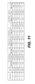
- FIG. 11 illustrates a table that reveals three measures for three alternative configurations of a dispersion compensation circuit.
- An apparatus and method for equalizing a received serial data signal uses non-traditional electronic dispersion compensation techniques applied to an electronic version of a data signal transmitted from a remote transmitter.
- the non-traditional electronic dispersion techniques include various improvements to a digital filter deployed in the channel receiver.
- the digital filter be coupled with a controller programmed to adjust the tap coefficients and controllably deploy a fractional unit interval tap spacing over a total tap range of at least three unit intervals in response to a residual ISI and a noise enhancement penalty.
- the controller is programmed to minimize the sum of the residual inter-symbol interference (ISI) and a noise enhancement penalty.
- ISI inter-symbol interference
- the sum of the residual ISI and the noise enhancement penalty are more closely attributable to link performance than conventional EDC techniques, which force the residual ISI to zero.
- the two taps closest to a main or reference tap can be positive. That is, positive coefficient values can be associated with each of these taps to increase the amplitude of the signal.
- the remaining taps can be adjusted to reduce ISI.
- a main or reference tap can be located anywhere across the set of all taps. An asymmetric tap arrangement can be helpful in properly correcting received waveforms with any asymmetry. However, it is preferred that at least two precursor taps be allocated to provide sufficient receiver responsiveness.
- the controller is arranged to provide a set of tap coefficients such that the sum of all tap coefficients normalized by a main or reference tap value is set to a value that approximates unity.
- the sum of all tap coefficients can be constrained within a range of about 0.8 to 1.2. In this way, the overall amplitude of the received and corrected signal is not far from the original signal value. Within that constraint the coefficient values are manipulated to minimize the ISI.
- the constraints are implemented using digital control logic, which is effective in an automated scheme using mean square error as the figure of merit for making the adjustments.
- the constraints greatly reduce the range of possible solutions that an algorithmic approach need to apply to determine an optimal solution for present link conditions as manifested in the electronic representation of the received signal.
- the constraints also reduce the likelihood of the controller misidentifying local minimums that might not be associated with optimal link performance.
- a set of predetermined coefficient values can be used to configure a digital filter in the dispersion compensation circuit to effectively maximize the receive signal for received waveforms having inter-symbol interference from about 2 dB to 5 dB.
- the set of coefficients can be defined as a function of a coefficient value for the adjacent taps to a reference, where a coefficient value associated with the reference tap is one and the coefficient values for the adjacent taps is about 0.38.
- the coefficient value for taps further removed from the reference tap is determined from the product of ⁇ 1 ⁇ 2 and the coefficient value for the adjacent taps, or ⁇ 0.19.
- FIG. 3 illustrates a block diagram of an embodiment of an improved controller 300 for adjusting a dispersion compensation circuit 110 .
- the controller 300 receives a quality signal on connection 125 from the detector 120 and sends configuration information on connection 315 to the M-tap FFE of the dispersion compensation circuit 110 to adaptively modify the eye diagram of the received signal on connection 115 .
- the quality signal is an error signal generated by a mean square error detector.
- the improved controller 300 includes a logic engine 310 , a tap constraint store 320 , a coefficient constraint store 322 , residual ISI logic 312 , noise enhancement penalty (NEP) logic 314 , coefficient generation logic 330 , and tap location logic 340 .
- the logic engine 310 or coordinating logic receives the quality signal via a suitable interface as well as information from the tap constraint store 320 and the coefficient constraint store 322 indicative of one or more tap constraints and one or more coefficient constraints that should be employed when generating configuration information.
- the configuration information generated and communicated by the logic engine 310 to the dispersion compensation circuit 110 defines characteristics of a digital filter.
- the digital filter can be implemented as an M-tap FFE, where M is a positive integer that identifies the number of taps present in the digital filter.
- the logic engine 310 executes one or more executable instructions in the residual ISI logic 312 to generate a measure of ISI remaining in the received signal.
- the logic engine 310 executes one or more executable instructions in the NEP logic 314 to generate a measure of the additional noise present in the equalized or adjusted receive signal.
- the logic engine 310 executes one or more executable instructions in the tap location logic 340 in accordance with one or more tap constraints as provided from the tap constraint store 320 to identify suitable delay times that are communicated in the configuration information to the dispersion compensation circuit 110 .
- the logic engine 310 executes one or more executable instructions in the coefficient generation logic 330 in accordance with one or more coefficient constraints as provided from the coefficient constraint store 322 that when applied in the digital filter will result in an equalized receiver output signal that minimizes a mathematical combination of the measure of the residual ISI and the noise enhancement penalty.
- the identified coefficient values for the identified taps are also communicated in the configuration information to the dispersion compensation circuit 110 .
- the one or more tap constraints will identify a reference tap location, a tap interval and a total tap coverage as an integer multiple of a UI. Given this information, the tap location logic 340 can provide the necessary configuration information to the M-tap FFE in the dispersion compensation circuit.
- the total tap coverage is the product of the tap interval and the total number of taps less one. For communication links using optical media (e.g., fiber), a total tap coverage of at least 3UI is preferred.
- Additional tap constraints may include a range of acceptable tap intervals (e.g. from about 0.3UI to about 0.7UI).
- the M-Tap FFE include 7 or more taps to achieve 3UI of coverage when a tap interval of 0.5UI is used.
- Other tap constraints may define a minimum number of precursor taps such as at least two precursor taps. When two precursor taps and seven total taps are defined, the resulting digital filter is asymmetric with respect to the number of remaining taps on the opposing or post-cursor side of the reference tap.
- Still another tap constraint may include a comparison of a pulse spread of a received signal with a function of the number of taps and a fractional unit interval to ensure that the taps are located to cover at least the spread of the received signal.
- Another tap constraint may include a minimum tap coverage of at least an integer multiple of the UI of the received signal.
- the one or more coefficient constraints will identify a unity coefficient value in association with the reference tap.
- the coefficient constraints may further include ensuring that the sign associated with the coefficient values for adjacent taps to the reference tap is positive.
- the coefficient constraints may also include a range for a sum of all coefficient values for coefficients associated with taps other than the reference tap. For example, the range for the sum of coefficient values applied to the taps other than the reference tap is from about 0.8 to about 1.2.
- FIG. 4 illustrates a block diagram of an embodiment of the multiple-tap feed-forward equalizer (M-tap FFE) 400 .
- a time-varying signal is received on connection 17 and is applied at each instance of the precursor taps 402 , the main or reference tap 404 , and each instance of the post-cursor taps 406 .
- all but the first of the precursor taps 402 and the last of the post-cursor taps 406 have a delay element 410 both before and after the tap.
- the delay elements 410 may each provide a similar delay in the received signal having a duration that is a fraction of the unit interval of the received data signal.
- Each of the precursor taps 402 , the main or reference tap 404 and the post-cursor taps 406 is coupled to a respective variable gain amplifier 415 that adjusts the magnitude of the received signal at its input in accordance with a coefficient value provided at a respective control input.
- the respective outputs generated by the variable gain amplifiers 415 are forwarded to adders 420 with adder 420 b arranged to provide the sum of all weighted tap outputs on connection 115 .
- a coefficient value corresponding to tap location C n ⁇ L is provided at the control input of the variable gain amplifier arranged to receive the input signal without delay, where L is a positive integer and the total number of taps is 2L+1.
- a coefficient value corresponding to C n ⁇ 1 is provided at the control input of the variable gain amplifier arranged to receive the delayed receive signal from the precursor tap adjacent to the main tap 404 .
- a coefficient value corresponding to the main or reference tap location C n is provided at the control input of the variable gain amplifier arranged to receive the delayed receive signal from the main tap 404 .
- a coefficient value corresponding to C n+1 is provided at the control input of the variable gain amplifier arranged to receive the delayed receive signal from the post-cursor tap adjacent to the main tap 404 .
- a coefficient value corresponding to tap location C n+L is provided at the control input of the variable gain amplifier arranged to receive the input signal after being delayed by all delay elements 410 a - 410 m .
- M is a positive integer indicative of the number of taps in the M-Tap FFE 400 .
- the M-Tap FFE 400 includes at least two precursor taps, which are arranged before the main or reference tap 404 .
- the M-Tap FFE 400 includes at least two post-cursor taps, which follow the main or reference tap 404 .
- the M-Tap FFE 400 is a symmetric digital filter as there are L precursor taps and L post-cursor taps.
- FIG. 5 illustrates an alternative embodiment of the M-Tap FFE 500 .
- a time-varying signal is received on connection 17 and is applied at each instance of the precursor taps 502 , the main or reference tap 504 , and each instance of the post-cursor taps 506 .
- all but the first of the precursor taps 502 and the last of the post-cursor taps 506 have a delay element 510 both before and after the tap.
- the delay elements 510 a - 510 e may each provide a different delay in the received signal having a duration that is a fraction of the unit interval of the received data signal.
- Each of the precursor taps 502 , the main or reference tap 504 and the post-cursor taps 506 is coupled to a respective variable gain amplifier 515 that adjusts the magnitude of the received signal at its input in accordance with a coefficient value provided at a respective control input.
- the respective outputs generated by the variable gain amplifiers 515 are forwarded to adders 520 with adder 520 c arranged to provide the sum of all weighted tap outputs on connection 525 .
- a coefficient value corresponding to tap location C n ⁇ 3 is provided at the control input of the variable gain amplifier arranged to receive the input signal without delay.
- a coefficient value corresponding to C n ⁇ 2 is provided at the control input of the variable gain amplifier arranged to receive the delayed receive signal from the precursor tap next closest to the main tap 504 .
- a coefficient value corresponding to C n ⁇ 1 is provided at the control input of the variable gain amplifier arranged to receive the delayed receive signal from the precursor tap adjacent to the main tap 504 .
- a coefficient value corresponding to the main or reference tap location C n is provided at the control input of the variable gain amplifier arranged to receive the delayed receive signal from the main tap 504 .
- a coefficient value corresponding to C n+1 is provided at the control input of the variable gain amplifier arranged to receive the delayed receive signal from the post-cursor tap adjacent to the main tap 504 .
- a coefficient value corresponding to tap location C n+2 is provided at the control input of the variable gain amplifier arranged to receive the input signal after being delayed by all delay elements 510 a - 510 e .
- the M-Tap FFE 500 is an asymmetric digital filter consisting of six total taps.
- each of the delay elements 510 may be implemented as a combination of a similar fixed delay, ⁇ , and a controllable additive delay t n .
- each of the controllable delays may be adjusted so that the total delay prior to a tap can be adjusted as may be desired.
- the delay introduced by delay element 510 a is the sum of ⁇ and t n ⁇ 2
- the delay introduced by delay element 510 b is the sum of ⁇ and t n ⁇ 1
- the delay introduced by delay element 510 c is the sum of ⁇ and t n , etc.
- a controllable delay element can be implemented electrically by varying one or more characteristics of a resistor, a capacitor or elements that exhibit electrical resistance or capacitance.
- the present controller and methods are not limited to any particular mechanism for controllably introducing a variable delay in a received signal.
- each of the delay elements 510 may be implemented as a controllable delay t n only. Either implementation will enable a tap delay or tap location adjustment to controllably manipulate a fractional unit interval between adjacent taps in a digital filter. Such tap delay or tap location adjustments can be applied to taps adjacent to a main or reference tap or another defined tap or taps.
- FIG. 6A includes an embodiment of an eye diagram 600 after equalization with the dispersion compensation circuit 400 of FIG. 3 .
- Signal trace 602 corresponds to a superposition of samples of a received serial data signal over 1UI of the transmitted data signal. Accordingly, the signal trace 602 shows a pulse spread 610 of 1UI or +/ ⁇ 0.5UI.
- a total tap coverage defined as the product of the tap spacing and a total number of taps minus 1, should stretch to at least the pulse spread of the received signal. For communications links using optical media, a total tap coverage of at least 3UI is preferred.
- additional constraints do not excessively reduce signal amplitude while reducing ISI. It is preferred that the sum of the penalty caused by the residual ISI and the noise enhancement penalty should be minimized. This function (i.e., the sum of residual ISI and the noise enhancement penalty) is more closely associated with communication link performance than the conventional method of forcing the residual ISI to zero.
- the coefficient value for the taps adjacent to the main or reference tap can be positive. This will increase the amplitude of the signal. Thus, reducing the penalty introduced in the conventional method, which significantly reduces signal amplitude.
- the coefficient values and the signs associated with the remaining taps can be used to close or minimize the residual ISI. It is proposed that the sum of all coefficient values, normalized by the main tap, be set to a value that is not far from unity. For example, the total range for the sum of coefficient values could be from about 0.8 to 1.2. In this way, the amplitude of the equalized signal is not far from the original signal value.
- the coefficient values applied to the taps (other than the reference tap) can be manipulated to minimize ISI.
- FIGS. 6B and 6C illustrate alternative embodiments of example tap locations generated by the controller 300 of FIG. 3 .
- plot 650 defines a digital filter having a main or reference tap at location 652 , a fixed fractional UI 654 of 0.5, and a total tap coverage 660 across a total of 21 taps. It should be understood that plot 650 is presented as an example configuration. Improvements can be shown for a digital filter having 7 total taps with a fractional UI of 0.5 between adjacent taps. Alternative delays (i.e., tap interval) ranging from about 0.3UI to about 0.7UI are contemplated and would also achieve desirable results.
- the FFE using 3 taps total with the taps spaced 1UI from each other results in a total center of eye penalty after equalization of 1.75 dB, yielding a relatively small gain of about 0.85 dB.
- the coefficient values are optimized at about 0.09, ⁇ 0.45, 0.36, 1.0, 0.36, ⁇ 0.45, 0.09.
- the total penalty is 1.1 dB in noise enhancement, leading to a 1.5 dB penalty reduction.
- Some additional optical waveforms were processed through a 7 tap filter using the same fractional UI of 0.5 between adjacent taps.
- a first waveform with an original vertical closure penalty of 2.2 was provided to the improved dispersion compensation circuit 110 .
- the coefficient values are 0.04, ⁇ 0.31, 0.27, 1, 0.27, ⁇ 0.32, 0.04.
- the residual ISI was 0.39 dB.
- the increased noise penalty from the additional signal is 0.63 dB.
- the total remaining penalty is 1.02 dB, resulting in a penalty reduction of 1.18 dB.
- the tap coefficient values are about ⁇ 0.12, 1, ⁇ 0.12.
- the signal amplitude is reduced to about 0.76, resulting in a net penalty reduction of only 0.58 dB.
- a second waveform with an original vertical closure penalty of 3.3 was provided to the improved dispersion compensation circuit 110 .
- the coefficient values are 0.04, ⁇ 0.31, 0.27, 1, 0.27, ⁇ 0.32, 0.04.
- the residual ISI was 1.09 dB.
- the increased noise penalty from the additional signal is 0.63 dB.
- the total remaining penalty is 1.72 dB, resulting in a penalty reduction of 1.61 dB.
- the tap coefficient values are about ⁇ 0.16, 1, ⁇ 0.16.
- the signal amplitude is reduced to about 0.68, resulting in a net penalty reduction of only 0.86 dB.
- a third waveform with an original vertical closure penalty of 4.1 was provided to the improved dispersion compensation circuit 110 .
- the coefficient values are 0.08, ⁇ 0.48, 0.40, 1, 0.40, ⁇ 0.48, 0.08.
- the residual ISI was 0.69 dB.
- the increased noise penalty from the additional signal is 1.28 dB.
- the total remaining penalty is 1.97 dB, resulting in a penalty reduction of 2.1 dB.
- the tap coefficient values are about ⁇ 0.20, 1, ⁇ 0.20.
- the signal amplitude is reduced to about 0.68, resulting in a net penalty reduction of only 1.36 dB.
- Plot 670 defines a digital filter having a main or reference tap at location 652 , a total tap coverage 660 of +/ ⁇ 5UI using a total of 21 taps with variable fractional UI delays.
- a first tap separation of a first fractional UI 674 is defined between the reference tap and the adjacent taps. This first fractional UI 674 is defined between the third taps and the fourth taps, between the fourth taps and the fifth taps and again between the seventh taps and the eighth taps and the eighth taps and the ninth taps from the reference tap 652 .
- a second tap separation of a second fractional UI 676 is defined between the first taps and the second taps and the second taps and the third taps and again between the fifth taps and the sixth taps and between the sixth taps and the seventh taps from the reference tap 652 .
- the second fractional UI 676 is wider (i.e., longer in time) than the first fractional UI 674 .
- This second fractional UI 676 can be accomplished by applying a correspondingly longer delay line between adjacent taps. It should be understood that other tap placements are possible by varying the time delay between the taps of the digital filter. It should be understood that plot 670 is presented as an example configuration.
- Table I shows a first simulation using fixed delays between filter taps relative to the main or reference tap and variable coefficient values or weights for each of the taps.
- the coefficient values were optimized to achieve a relatively flat center eye opening of about 0.15UI.
- the coefficient values are 0.015, ⁇ 0.372, 0.340, 1, 0.233, ⁇ 0.257, 0.041.
- the residual ISI was 1.4 dB.
- the increased noise penalty from the additional signal is 0.7 dB.
- the resulting net gain in the link budget is 1.9 dB.
- FIG. 7A includes a plot illustrating an original (non-equalized) eye diagram.
- FIG. 7B includes a plot showing the resulting equalized eye diagram when the equalizer is configured with the tap delays and coefficient values from Table I.
- Table II shows a second simulation using variable tap delays relative to the distance from the main or reference tap and variable coefficient values or weights for each of the taps.
- the coefficient values were optimized to achieve a relatively flat center eye opening of about 0.15UI.
- the coefficient values are ⁇ 0.199, ⁇ 0.223, 0.360, 1, 0.360, ⁇ 0.158, ⁇ 0.140.
- the residual ISI was 0.47 dB.
- the increased noise penalty from the additional signal is 0.72 dB.
- the resulting net gain in the link budget is 2.77 dB.
- FIG. 8A includes a plot illustrating an original (non-equalized) eye diagram.
- FIG. 8B includes a plot showing the resulting equalized eye diagram when the equalizer is configured with the tap delays and coefficient values from Table II.
- FIG. 9 illustrates a flow diagram of an embodiment of a method 900 for equalizing a received serial data signal.
- the method 900 begins with block 902 where a signal is received from a detector coupled to an output of a dispersion compensation circuit.
- the signal may be a sampled representation of the output of the dispersion compensation circuit or may be an output from any number of circuits that generate an electrical signal indicative of the quality of the signal at the output of the dispersion compensation circuit.
- These circuits can include an error detection or error correction circuit, an eye monitor circuit, a mean square error detector, a signal spectrum monitor.
- the arrangements and operating description of these well known signal quality detectors are incorporated by reference and are understood by those skilled in art.
- a tap constraint may include one or more of a minimum number of taps, a tap separation between adjacent taps, a total tap coverage or range of fractional UI spaces between adjacent taps, a minimum number of precursor taps, a location of a main or reference tap, and a comparison of a pulse spread of a received signal with a function of a number of taps and a fractional UI between adjacent taps.
- a coefficient constraint may include one or more of ensuring that a sign associated with adjacent taps to a reference tap is positive, a range for the sum of all coefficient values (e.g., from about 0.8 to 1.2), a predetermined value for a reference or main tap (e.g., the real number 1.0), and a predetermined set of coefficient values for application to be applied under defined circumstances.
- the logic engine or alternatively a dedicated circuit or processor is used to generate a measure of the ISI in a receive signal processed by the dispersion compensation circuit.
- the logic engine or alternatively a dedicated circuit or processor is used to generate a measure of a noise enhancement penalty in a receive signal processed by the dispersion compensation circuit.
- the logic engine iteratively generates a set of coefficient values that when applied to the dispersion compensation circuit (e.g., to the taps of a FFE digital filter) will result in an equalized receiver signal that minimizes a mathematical combination of the ISI and the noise enhancement penalty as measured in block 906 and in block 908 , respectively.
- a tap delay adjustment is communicated to dispersion compensation circuit to controllably manipulate a fractional UI between adjacent taps in a digital filter.
- FIG. 10 illustrates a flow diagram of an embodiment of an alternative method 1000 for equalizing a received serial data signal.
- the method 1000 begins with block 1002 where it is determined that a received signal is degraded due to a bandwidth limited communication channel.
- a bandwidth limited communication channel will typically exhibit a symmetrical eye diagram.
- one or more measures of symmetry of the eye diagram as produced by an eye monitor may be used to determine when a received signal is degraded due to transmission via a bandwidth limited communication channel.
- a set of coefficient values are applied to a dispersion compensation circuit such as the digital filter illustrated in FIG. 4 .
- the coefficient values are a function of a coefficient value for taps adjacent to a reference tap of the digital filter and the coefficient value for the reference tap is the real number one.
- the table includes three measures for three alternative configurations of a dispersion compensation circuit 100 .
- the first of the alternative configurations reveals a residual ISI, a net error figure (NEF), and net signal gain for the case where each of the coefficient values is optimized.
- NEF net error figure
- the second of the alternative configurations reveals the residual ISI, NEF and the net signal gain for the case where the tap coefficient value for the adjacent tap to the reference tap is fixed at 0.377.
- the third of the alternative configurations reveals the same measures for the case where the tap coefficient value for the adjacent tap to the reference tap is optimized.
- controller and methods for equalizing a received serial data signal have been described in association with the illustrated embodiments, those skilled in the art will understand that a variety of logical configurations may be used for this purpose. Thus, the controller and methods for equalizing a received serial data signal are not limited to the described embodiments.
Abstract
Description
Here Cn is the value of the reference tap weight and n is the location of the reference tap, and Ci is the tap weight of the ith tap. In this example, Cn=1, n=2, and Ci=−0.15, 1, −0.15, respectively, for i=1, 2, 3.
This noise caused an additional noise penalty,
which is 0.10 dB based on tap weights of −0.15, 1, and −0.15.
| TABLE I | ||
| Tap Delays | ||
| −1.50 | −1.00 | −0.50 | 0.00 | 0.50 | 1.00 | 1.50 | ||
| Coefficient | 0.015 | −0.372 | 0.340 | 1.00 | 0.233 | −0.257 | 0.041 |
| Value | |||||||
| TABLE II | ||
| Tap Delays | ||
| −1.05 | −0.95 | −0.10 | 0.00 | 0.10 | 0.95 | 1.05 | ||
| Coefficient | −0.199 | −0.223 | 0.360 | 1.00 | 0.360 | −0.158 | −0.140 |
| Value | |||||||
C(−3)=C(3)=C(−2)=C(2)=0.5*C(−1); C(−1)=C(1)
Claims (20)
Priority Applications (2)
| Application Number | Priority Date | Filing Date | Title |
|---|---|---|---|
| US13/622,508 US8873615B2 (en) | 2012-09-19 | 2012-09-19 | Method and controller for equalizing a received serial data stream |
| TW102130659A TWI521898B (en) | 2012-09-19 | 2013-08-27 | Method and controller for equalizing a received serial data stream |
Applications Claiming Priority (1)
| Application Number | Priority Date | Filing Date | Title |
|---|---|---|---|
| US13/622,508 US8873615B2 (en) | 2012-09-19 | 2012-09-19 | Method and controller for equalizing a received serial data stream |
Publications (2)
| Publication Number | Publication Date |
|---|---|
| US20140079111A1 US20140079111A1 (en) | 2014-03-20 |
| US8873615B2 true US8873615B2 (en) | 2014-10-28 |
Family
ID=50274430
Family Applications (1)
| Application Number | Title | Priority Date | Filing Date |
|---|---|---|---|
| US13/622,508 Active 2032-12-06 US8873615B2 (en) | 2012-09-19 | 2012-09-19 | Method and controller for equalizing a received serial data stream |
Country Status (2)
| Country | Link |
|---|---|
| US (1) | US8873615B2 (en) |
| TW (1) | TWI521898B (en) |
Cited By (1)
| Publication number | Priority date | Publication date | Assignee | Title |
|---|---|---|---|---|
| US11881971B2 (en) * | 2021-09-30 | 2024-01-23 | Inspur Suzhou Intelligent Technology Co., Ltd. | Adaptive PAM4 decision feedback equalization circuit |
Families Citing this family (12)
| Publication number | Priority date | Publication date | Assignee | Title |
|---|---|---|---|---|
| US9886402B2 (en) * | 2012-12-20 | 2018-02-06 | Nvidia Corporation | Equalization coefficient search algorithm |
| CN109076032B (en) | 2016-02-23 | 2020-09-25 | 华为技术有限公司 | FFE assisted CDR to calibrate phase offset and improve baud rate sample phase detector gain |
| US10225016B1 (en) * | 2016-06-28 | 2019-03-05 | Amazon Technologies, Inc. | Optical power and chromatic dispersion equalization system |
| US9900121B1 (en) * | 2016-09-08 | 2018-02-20 | Futurewei Technologies, Inc. | Apparatus, system, and method for reducing a number of intersymbol interference components to be suppressed |
| US10135606B2 (en) * | 2016-10-27 | 2018-11-20 | Macom Connectivity Solutions, Llc | Mitigating interaction between adaptive equalization and timing recovery |
| CN108631752B (en) * | 2017-03-16 | 2021-12-24 | 航天信息股份有限公司 | Shaping filter and shaping method thereof |
| US11243356B2 (en) * | 2017-07-21 | 2022-02-08 | Telefonaktiebolaget Lm Ericsson (Publ) | Chromatic dispersion compensation |
| US10911272B2 (en) * | 2019-01-31 | 2021-02-02 | Taiwan Semiconductor Manufacturing Company, Ltd. | Multi-tap decision feed-forward equalizer with precursor and postcursor taps |
| US11290184B2 (en) * | 2019-03-01 | 2022-03-29 | Molex, Llc | Switchable dispersion compensating module |
| US11798618B2 (en) * | 2019-11-15 | 2023-10-24 | Rohde & Schwarz Gmbh & Co. Kg | Signal analyzer and method of processing data from an input signal |
| US11336378B2 (en) * | 2020-04-17 | 2022-05-17 | Cisco Technology, Inc. | Techniques for applying equalization to signals received over multimode fiber links |
| US11153129B1 (en) * | 2020-06-01 | 2021-10-19 | International Business Machines Corporation | Feedforward equalizer with programmable roaming taps |
Citations (77)
| Publication number | Priority date | Publication date | Assignee | Title |
|---|---|---|---|---|
| US5157395A (en) * | 1991-03-04 | 1992-10-20 | Crystal Semiconductor Corporation | Variable decimation architecture for a delta-sigma analog-to-digital converter |
| US5428605A (en) * | 1993-05-14 | 1995-06-27 | Telefonaktiebolaget Lm Ericsson | Method and echo canceller for echo cancellation with a number of cascade-connected adaptive filters |
| US5596677A (en) * | 1992-11-26 | 1997-01-21 | Nokia Mobile Phones Ltd. | Methods and apparatus for coding a speech signal using variable order filtering |
| US5774564A (en) * | 1993-10-13 | 1998-06-30 | Sharp Kabushiki Kaisha | Active controller using lattice-type filter and active control method |
| US5815496A (en) * | 1995-09-29 | 1998-09-29 | Lucent Technologies Inc. | Cascade echo canceler arrangement |
| US5841810A (en) * | 1997-01-30 | 1998-11-24 | National Semiconductor Corporation | Multiple stage adaptive equalizer |
| US5864798A (en) * | 1995-09-18 | 1999-01-26 | Kabushiki Kaisha Toshiba | Method and apparatus for adjusting a spectrum shape of a speech signal |
| US6061008A (en) * | 1997-12-19 | 2000-05-09 | Rockwell Science Center, Inc. | Sigma-delta-sigma modulator for high performance analog-to-digital and digital-to-analog conversion |
| US6195383B1 (en) * | 1998-11-28 | 2001-02-27 | Matra Marconi Space Uk Limited | Digital signal processing apparatus for frequency de-hopping |
| US6212144B1 (en) * | 1998-03-13 | 2001-04-03 | Fujitsu Limited | Method and apparatus for reading data |
| US6347123B1 (en) * | 1998-07-10 | 2002-02-12 | Qualcomm Incorporated | Low-current sample rate converter |
| US20020051502A1 (en) * | 1998-12-14 | 2002-05-02 | Lennart Mathe | Low-power programmable digital filter |
| US6445735B1 (en) * | 1999-02-08 | 2002-09-03 | Visteon Global Technologies, Inc. | Switched bandwidth digital filters with reduced transients during switching |
| US20020132590A1 (en) * | 2001-03-17 | 2002-09-19 | Koninklijke Philips Electronics N.V. | Radio transceiver |
| US20030016605A1 (en) * | 2001-07-18 | 2003-01-23 | Nec Corporation | Optical receiving device, waveform optimization method for optical data signals, and waveform optimization program for optical data signals |
| US20030053243A1 (en) * | 2001-05-30 | 2003-03-20 | Nec Corporation | Positioning control apparatus and method capable of reducing relative position error without increasing gain and frequency band of transfer characteristics of control system |
| US20040018825A1 (en) * | 2000-05-16 | 2004-01-29 | Elmar Wagner | Circuit configuration for tolerance correction in a frequency demodulator |
| US20040114936A1 (en) * | 2002-01-30 | 2004-06-17 | Takashi Sugihara | Disperse equalizer and disperse equalizing method |
| US20040141756A1 (en) * | 2003-01-16 | 2004-07-22 | Fujitsu Limited | Method and apparatus for adjusting filter device |
| US20040152418A1 (en) * | 2002-11-06 | 2004-08-05 | Engim, Inc. | Unified digital front end for IEEE 802.11g WLAN system |
| US20040179849A1 (en) * | 2003-03-14 | 2004-09-16 | Tetsuya Miyazaki | Optical receiver and method for controlling dispersion compensation |
| US20040199559A1 (en) * | 2003-04-07 | 2004-10-07 | Mcadam Matthew W. | Flexible adaptation engine for adaptive transversal filters |
| US6804695B1 (en) * | 2000-11-22 | 2004-10-12 | Marvell International Ltd. | Method and apparatus for constraining tap coefficients in an adaptive finite impulse response filter |
| US6873704B1 (en) * | 1998-10-13 | 2005-03-29 | Samsung Electronics Co., Ltd | Apparatus for removing echo from speech signals with variable rate |
| US6947497B1 (en) * | 1999-07-12 | 2005-09-20 | Samsung Electronics Co., Ltd. | Digital signal receiver and method for receiving digital signal |
| US20050207515A1 (en) * | 2001-11-14 | 2005-09-22 | Henrik Jensen | Digital demodulation |
| US20060067699A1 (en) | 2004-09-24 | 2006-03-30 | Sethumadhavan Chandrasekhar | Equalizer having tunable optical and electronic dispersion compensation |
| US20060140262A1 (en) * | 2003-02-14 | 2006-06-29 | Maarten Kuijk | Low voltage multistage adaptive equalizer |
| US7099822B2 (en) * | 2002-12-10 | 2006-08-29 | Liberato Technologies, Inc. | System and method for noise reduction having first and second adaptive filters responsive to a stored vector |
| US20060198464A1 (en) * | 2005-03-07 | 2006-09-07 | Fujitsu Limited | Distortion compensation apparatus |
| US7149474B1 (en) * | 1999-11-02 | 2006-12-12 | Broadcom Corporation | Wireless cable replacement system |
| US20070110199A1 (en) * | 2005-11-15 | 2007-05-17 | Afshin Momtaz | Receive equalizer with adaptive loops |
| US20070297804A1 (en) * | 2006-06-27 | 2007-12-27 | Fujitsu Limited | High-speed dispersion compensation control apparatus |
| US20080025730A1 (en) * | 2006-06-29 | 2008-01-31 | Giovannini Thomas J | Method and apparatus for autonomous adaptation of an optical dispersion compensation ("ODC") module |
| US20080036883A1 (en) * | 2006-08-14 | 2008-02-14 | Sony Corporation | Image pickup apparatus, defect compensation device, and defect-compensating method |
| US20080107166A1 (en) * | 2006-11-06 | 2008-05-08 | Samsung Electronics Co., Ltd. | Adaptive equalizer and adaptive equalization method |
| US20080137778A1 (en) * | 2006-12-07 | 2008-06-12 | Fujitsu Limited | Receiving device and receiving method |
| US20080167793A1 (en) * | 2007-01-10 | 2008-07-10 | Denso Corporation | Apparatus for filtering measured analog signal used to control vehicle engine |
| US20080187323A1 (en) * | 2007-02-06 | 2008-08-07 | Fujitsu Limited | Optical receiver and controlling method thereof, and optical transmission system |
| US20080279563A1 (en) * | 2005-12-20 | 2008-11-13 | Huade Shu | Apparatus and Method for Self-Adaptive Dispersion Compensating |
| US20080310855A1 (en) * | 2007-06-13 | 2008-12-18 | Kenichi Ogawa | Optical Transmission Equipment and Method for Controlling Thereof |
| US20090047025A1 (en) | 2007-06-04 | 2009-02-19 | Jin Hong | Multiple Electrical Level Dispersion Tolerant Optical Apparatus |
| US20090067559A1 (en) * | 1998-11-13 | 2009-03-12 | Azazzi Oscar E | System and method for high-speed decoding and isi compensation in a multi-pair transceiver system |
| US20090067783A1 (en) * | 2007-09-07 | 2009-03-12 | Azea Networks Limited | Method of tuning an adjustable dispersion compensator |
| US20090116844A1 (en) * | 2007-11-07 | 2009-05-07 | Fujitsu Limited | Electrical-dispersion compensating apparatus, optical receiving apparatus, and optical receiving method |
| US7548726B1 (en) * | 1999-10-21 | 2009-06-16 | Broadcom Corporation | Adaptive radio transceiver with a bandpass filter |
| US20090190646A1 (en) * | 2008-01-28 | 2009-07-30 | Nec Electronics Corporation | Adaptive equalizer and adaptive equalization method |
| US20090221254A1 (en) * | 2008-02-29 | 2009-09-03 | Hidetoshi Kawauchi | Reception apparatus, reception method and program |
| US20090238563A1 (en) * | 2008-03-21 | 2009-09-24 | Yasuyuki Fukashiro | Optical Signal Transmission Apparatus |
| US20090296798A1 (en) * | 2006-04-05 | 2009-12-03 | Agere Systems Inc,. | Hsdpa co-processor for mobile terminals |
| US20090317079A1 (en) * | 2006-11-30 | 2009-12-24 | Nobuhide Yoshida | Dispersion determining apparatus and automatic dispersion compensating system using the same |
| US20090315871A1 (en) * | 2007-02-26 | 2009-12-24 | Nec Display Solutions, Ltd. | Image display system, image signal transmitter and image display unit |
| US20090317092A1 (en) * | 2008-06-19 | 2009-12-24 | Fujitsu Limited | Optical receiving apparatus and digital receiving circuit |
| US7664394B2 (en) | 2005-06-30 | 2010-02-16 | Clariphy Communications, Inc. | Testing of receivers with separate linear O/E module and host used in communication links |
| US20100054759A1 (en) * | 2008-08-29 | 2010-03-04 | Fujitsu Limited | Method for Electric Power Supply of Optical Receiver, Digital Signal Processing Circuit, and Optical Receiver |
| US20100067917A1 (en) * | 2008-09-18 | 2010-03-18 | Fujitsu Limited | Optical transmission apparatus, optical transmission method, and optical transceiver |
| US20100092185A1 (en) * | 2008-10-10 | 2010-04-15 | Fujitsu Limited | Optical receiver |
| US20100124418A1 (en) | 2008-11-17 | 2010-05-20 | Finisar Corporation | Transmission of eye information from opto-electronic modules |
| US20100142946A1 (en) * | 2008-11-28 | 2010-06-10 | Fujitsu Limited | Chromatic dispersion monitor and method, chromatic dispersion compensator |
| US20100158537A1 (en) * | 2008-12-22 | 2010-06-24 | Fujitsu Limited | Propagation apparatus and dispersion value setting method |
| US7778323B1 (en) * | 2005-01-27 | 2010-08-17 | National Semiconductor Corporation | System and method for providing a parameterized analog feedback loop for continuous time adaptive equalization incorporating low frequency attenuation gain compensation |
| US20100247095A1 (en) * | 2007-12-20 | 2010-09-30 | Fujitsu Limited | Wavelength division multiplexing apparatus and dispersion compensating method for optical signal |
| US20100266134A1 (en) * | 2009-04-17 | 2010-10-21 | Harman International Industries, Incorporated | System for active noise control with an infinite impulse response filter |
| US20100278528A1 (en) * | 2007-11-08 | 2010-11-04 | Fujitsu Limited | Coherent optical receiver |
| US20100316112A1 (en) * | 2009-06-15 | 2010-12-16 | Liang-Wei Huang | Communication signal receiver and signal processing method thereof |
| US20100322630A1 (en) * | 2009-06-19 | 2010-12-23 | Fujitsu Limited | Optical transmission apparatus and method |
| US20110052198A1 (en) * | 2009-08-31 | 2011-03-03 | Fujitsu Limited | Optical transmission device, transmission and reception module, optical transmission system, and wavelength dispersion compensation method in optical transmission device |
| US20110188854A1 (en) * | 2010-01-29 | 2011-08-04 | Toshiki Honda | Optical receiving apparatus and optical transmission system |
| US20110293270A1 (en) * | 2010-05-28 | 2011-12-01 | Hitachi, Ltd. | Optical receiver and optical transfer apparatus |
| US20110305453A1 (en) * | 2009-02-20 | 2011-12-15 | Nokia Siemens Networks Gmbh & Co. Kg | Method and arrangement for adaptive dispersion compensation |
| US20120020661A1 (en) * | 2009-03-30 | 2012-01-26 | Fujitsu Limited | Optical communication device and dispersion compensation method |
| US20120051754A1 (en) * | 2010-08-30 | 2012-03-01 | Fujitsu Limited | Optical receiver, method for receiving optical signal, and optical transmission system |
| US20120148265A1 (en) * | 2010-12-13 | 2012-06-14 | Electronics And Telecommunications Research Institute | Coherent optical receiving device capable of digital equalization of optical input, digital equalization method for optical input and coherent optical transmitting/receiving device |
| US8300744B2 (en) * | 2010-01-28 | 2012-10-30 | Korea Advanced Institute Of Science And Technology | Apparatus for rejecting image in receiver |
| US8306430B2 (en) * | 2006-05-30 | 2012-11-06 | Fujitsu Limited | Dispersion compensating apparatus and dispersion compensating method |
| US20130016968A1 (en) * | 2011-07-12 | 2013-01-17 | Fujitsu Limited | Tunable dispersion compensation device, optical reception apparatus, and method for controlling tunable dispersion compensation |
| US8478137B2 (en) * | 2010-02-12 | 2013-07-02 | Fujitsu Limited | Optical receiver |
-
2012
- 2012-09-19 US US13/622,508 patent/US8873615B2/en active Active
-
2013
- 2013-08-27 TW TW102130659A patent/TWI521898B/en not_active IP Right Cessation
Patent Citations (81)
| Publication number | Priority date | Publication date | Assignee | Title |
|---|---|---|---|---|
| US5157395A (en) * | 1991-03-04 | 1992-10-20 | Crystal Semiconductor Corporation | Variable decimation architecture for a delta-sigma analog-to-digital converter |
| US5596677A (en) * | 1992-11-26 | 1997-01-21 | Nokia Mobile Phones Ltd. | Methods and apparatus for coding a speech signal using variable order filtering |
| US5428605A (en) * | 1993-05-14 | 1995-06-27 | Telefonaktiebolaget Lm Ericsson | Method and echo canceller for echo cancellation with a number of cascade-connected adaptive filters |
| US5774564A (en) * | 1993-10-13 | 1998-06-30 | Sharp Kabushiki Kaisha | Active controller using lattice-type filter and active control method |
| US5864798A (en) * | 1995-09-18 | 1999-01-26 | Kabushiki Kaisha Toshiba | Method and apparatus for adjusting a spectrum shape of a speech signal |
| US6009083A (en) * | 1995-09-29 | 1999-12-28 | Lucent Technologies, Inc. | Cascade echo canceler arrangement |
| US5815496A (en) * | 1995-09-29 | 1998-09-29 | Lucent Technologies Inc. | Cascade echo canceler arrangement |
| US5841810A (en) * | 1997-01-30 | 1998-11-24 | National Semiconductor Corporation | Multiple stage adaptive equalizer |
| US6061008A (en) * | 1997-12-19 | 2000-05-09 | Rockwell Science Center, Inc. | Sigma-delta-sigma modulator for high performance analog-to-digital and digital-to-analog conversion |
| US6212144B1 (en) * | 1998-03-13 | 2001-04-03 | Fujitsu Limited | Method and apparatus for reading data |
| US6347123B1 (en) * | 1998-07-10 | 2002-02-12 | Qualcomm Incorporated | Low-current sample rate converter |
| US6873704B1 (en) * | 1998-10-13 | 2005-03-29 | Samsung Electronics Co., Ltd | Apparatus for removing echo from speech signals with variable rate |
| US20090067559A1 (en) * | 1998-11-13 | 2009-03-12 | Azazzi Oscar E | System and method for high-speed decoding and isi compensation in a multi-pair transceiver system |
| US6195383B1 (en) * | 1998-11-28 | 2001-02-27 | Matra Marconi Space Uk Limited | Digital signal processing apparatus for frequency de-hopping |
| US20020051502A1 (en) * | 1998-12-14 | 2002-05-02 | Lennart Mathe | Low-power programmable digital filter |
| US6445735B1 (en) * | 1999-02-08 | 2002-09-03 | Visteon Global Technologies, Inc. | Switched bandwidth digital filters with reduced transients during switching |
| US6947497B1 (en) * | 1999-07-12 | 2005-09-20 | Samsung Electronics Co., Ltd. | Digital signal receiver and method for receiving digital signal |
| US7548726B1 (en) * | 1999-10-21 | 2009-06-16 | Broadcom Corporation | Adaptive radio transceiver with a bandpass filter |
| US7149474B1 (en) * | 1999-11-02 | 2006-12-12 | Broadcom Corporation | Wireless cable replacement system |
| US20040018825A1 (en) * | 2000-05-16 | 2004-01-29 | Elmar Wagner | Circuit configuration for tolerance correction in a frequency demodulator |
| US6804695B1 (en) * | 2000-11-22 | 2004-10-12 | Marvell International Ltd. | Method and apparatus for constraining tap coefficients in an adaptive finite impulse response filter |
| US20020132590A1 (en) * | 2001-03-17 | 2002-09-19 | Koninklijke Philips Electronics N.V. | Radio transceiver |
| US20030053243A1 (en) * | 2001-05-30 | 2003-03-20 | Nec Corporation | Positioning control apparatus and method capable of reducing relative position error without increasing gain and frequency band of transfer characteristics of control system |
| US20030016605A1 (en) * | 2001-07-18 | 2003-01-23 | Nec Corporation | Optical receiving device, waveform optimization method for optical data signals, and waveform optimization program for optical data signals |
| US20050207515A1 (en) * | 2001-11-14 | 2005-09-22 | Henrik Jensen | Digital demodulation |
| US20040114936A1 (en) * | 2002-01-30 | 2004-06-17 | Takashi Sugihara | Disperse equalizer and disperse equalizing method |
| US20040152418A1 (en) * | 2002-11-06 | 2004-08-05 | Engim, Inc. | Unified digital front end for IEEE 802.11g WLAN system |
| US7099822B2 (en) * | 2002-12-10 | 2006-08-29 | Liberato Technologies, Inc. | System and method for noise reduction having first and second adaptive filters responsive to a stored vector |
| US20040141756A1 (en) * | 2003-01-16 | 2004-07-22 | Fujitsu Limited | Method and apparatus for adjusting filter device |
| US7894515B2 (en) * | 2003-02-14 | 2011-02-22 | Vrije Universiteit Brussel | Low voltage multistage adaptive equalizer |
| US20060140262A1 (en) * | 2003-02-14 | 2006-06-29 | Maarten Kuijk | Low voltage multistage adaptive equalizer |
| US20040179849A1 (en) * | 2003-03-14 | 2004-09-16 | Tetsuya Miyazaki | Optical receiver and method for controlling dispersion compensation |
| US20040199559A1 (en) * | 2003-04-07 | 2004-10-07 | Mcadam Matthew W. | Flexible adaptation engine for adaptive transversal filters |
| US7293055B2 (en) * | 2003-04-07 | 2007-11-06 | Pmc-Sierra, Inc. | Flexible adaptation engine for adaptive transversal filters |
| US20060067699A1 (en) | 2004-09-24 | 2006-03-30 | Sethumadhavan Chandrasekhar | Equalizer having tunable optical and electronic dispersion compensation |
| US7778323B1 (en) * | 2005-01-27 | 2010-08-17 | National Semiconductor Corporation | System and method for providing a parameterized analog feedback loop for continuous time adaptive equalization incorporating low frequency attenuation gain compensation |
| US20060198464A1 (en) * | 2005-03-07 | 2006-09-07 | Fujitsu Limited | Distortion compensation apparatus |
| US7664394B2 (en) | 2005-06-30 | 2010-02-16 | Clariphy Communications, Inc. | Testing of receivers with separate linear O/E module and host used in communication links |
| US20070110199A1 (en) * | 2005-11-15 | 2007-05-17 | Afshin Momtaz | Receive equalizer with adaptive loops |
| US20080279563A1 (en) * | 2005-12-20 | 2008-11-13 | Huade Shu | Apparatus and Method for Self-Adaptive Dispersion Compensating |
| US20090296798A1 (en) * | 2006-04-05 | 2009-12-03 | Agere Systems Inc,. | Hsdpa co-processor for mobile terminals |
| US8306430B2 (en) * | 2006-05-30 | 2012-11-06 | Fujitsu Limited | Dispersion compensating apparatus and dispersion compensating method |
| US20070297804A1 (en) * | 2006-06-27 | 2007-12-27 | Fujitsu Limited | High-speed dispersion compensation control apparatus |
| US20080025730A1 (en) * | 2006-06-29 | 2008-01-31 | Giovannini Thomas J | Method and apparatus for autonomous adaptation of an optical dispersion compensation ("ODC") module |
| US7872679B2 (en) * | 2006-08-14 | 2011-01-18 | Sony Corporation | Image pickup apparatus, defect compensation device, and defect-compensating method |
| US20080036883A1 (en) * | 2006-08-14 | 2008-02-14 | Sony Corporation | Image pickup apparatus, defect compensation device, and defect-compensating method |
| US20080107166A1 (en) * | 2006-11-06 | 2008-05-08 | Samsung Electronics Co., Ltd. | Adaptive equalizer and adaptive equalization method |
| US20090317079A1 (en) * | 2006-11-30 | 2009-12-24 | Nobuhide Yoshida | Dispersion determining apparatus and automatic dispersion compensating system using the same |
| US20080137778A1 (en) * | 2006-12-07 | 2008-06-12 | Fujitsu Limited | Receiving device and receiving method |
| US20080167793A1 (en) * | 2007-01-10 | 2008-07-10 | Denso Corporation | Apparatus for filtering measured analog signal used to control vehicle engine |
| US20080187323A1 (en) * | 2007-02-06 | 2008-08-07 | Fujitsu Limited | Optical receiver and controlling method thereof, and optical transmission system |
| US20090315871A1 (en) * | 2007-02-26 | 2009-12-24 | Nec Display Solutions, Ltd. | Image display system, image signal transmitter and image display unit |
| US20090047025A1 (en) | 2007-06-04 | 2009-02-19 | Jin Hong | Multiple Electrical Level Dispersion Tolerant Optical Apparatus |
| US20080310855A1 (en) * | 2007-06-13 | 2008-12-18 | Kenichi Ogawa | Optical Transmission Equipment and Method for Controlling Thereof |
| US20090067783A1 (en) * | 2007-09-07 | 2009-03-12 | Azea Networks Limited | Method of tuning an adjustable dispersion compensator |
| US20090116844A1 (en) * | 2007-11-07 | 2009-05-07 | Fujitsu Limited | Electrical-dispersion compensating apparatus, optical receiving apparatus, and optical receiving method |
| US20100278528A1 (en) * | 2007-11-08 | 2010-11-04 | Fujitsu Limited | Coherent optical receiver |
| US20100247095A1 (en) * | 2007-12-20 | 2010-09-30 | Fujitsu Limited | Wavelength division multiplexing apparatus and dispersion compensating method for optical signal |
| US20090190646A1 (en) * | 2008-01-28 | 2009-07-30 | Nec Electronics Corporation | Adaptive equalizer and adaptive equalization method |
| US20090221254A1 (en) * | 2008-02-29 | 2009-09-03 | Hidetoshi Kawauchi | Reception apparatus, reception method and program |
| US20090238563A1 (en) * | 2008-03-21 | 2009-09-24 | Yasuyuki Fukashiro | Optical Signal Transmission Apparatus |
| US20090317092A1 (en) * | 2008-06-19 | 2009-12-24 | Fujitsu Limited | Optical receiving apparatus and digital receiving circuit |
| US20100054759A1 (en) * | 2008-08-29 | 2010-03-04 | Fujitsu Limited | Method for Electric Power Supply of Optical Receiver, Digital Signal Processing Circuit, and Optical Receiver |
| US20100067917A1 (en) * | 2008-09-18 | 2010-03-18 | Fujitsu Limited | Optical transmission apparatus, optical transmission method, and optical transceiver |
| US20100092185A1 (en) * | 2008-10-10 | 2010-04-15 | Fujitsu Limited | Optical receiver |
| US20100124418A1 (en) | 2008-11-17 | 2010-05-20 | Finisar Corporation | Transmission of eye information from opto-electronic modules |
| US20100142946A1 (en) * | 2008-11-28 | 2010-06-10 | Fujitsu Limited | Chromatic dispersion monitor and method, chromatic dispersion compensator |
| US20100158537A1 (en) * | 2008-12-22 | 2010-06-24 | Fujitsu Limited | Propagation apparatus and dispersion value setting method |
| US20110305453A1 (en) * | 2009-02-20 | 2011-12-15 | Nokia Siemens Networks Gmbh & Co. Kg | Method and arrangement for adaptive dispersion compensation |
| US20120020661A1 (en) * | 2009-03-30 | 2012-01-26 | Fujitsu Limited | Optical communication device and dispersion compensation method |
| US20100266134A1 (en) * | 2009-04-17 | 2010-10-21 | Harman International Industries, Incorporated | System for active noise control with an infinite impulse response filter |
| US20100316112A1 (en) * | 2009-06-15 | 2010-12-16 | Liang-Wei Huang | Communication signal receiver and signal processing method thereof |
| US20100322630A1 (en) * | 2009-06-19 | 2010-12-23 | Fujitsu Limited | Optical transmission apparatus and method |
| US20110052198A1 (en) * | 2009-08-31 | 2011-03-03 | Fujitsu Limited | Optical transmission device, transmission and reception module, optical transmission system, and wavelength dispersion compensation method in optical transmission device |
| US8300744B2 (en) * | 2010-01-28 | 2012-10-30 | Korea Advanced Institute Of Science And Technology | Apparatus for rejecting image in receiver |
| US20110188854A1 (en) * | 2010-01-29 | 2011-08-04 | Toshiki Honda | Optical receiving apparatus and optical transmission system |
| US8478137B2 (en) * | 2010-02-12 | 2013-07-02 | Fujitsu Limited | Optical receiver |
| US20110293270A1 (en) * | 2010-05-28 | 2011-12-01 | Hitachi, Ltd. | Optical receiver and optical transfer apparatus |
| US20120051754A1 (en) * | 2010-08-30 | 2012-03-01 | Fujitsu Limited | Optical receiver, method for receiving optical signal, and optical transmission system |
| US20120148265A1 (en) * | 2010-12-13 | 2012-06-14 | Electronics And Telecommunications Research Institute | Coherent optical receiving device capable of digital equalization of optical input, digital equalization method for optical input and coherent optical transmitting/receiving device |
| US20130016968A1 (en) * | 2011-07-12 | 2013-01-17 | Fujitsu Limited | Tunable dispersion compensation device, optical reception apparatus, and method for controlling tunable dispersion compensation |
Non-Patent Citations (3)
| Title |
|---|
| Breyer et al., Comparison of OOK- and PAM-4 Modulation for 10GBits/s Transmission Over Up to 300m Polymer Optical Fiber, 2008, available at http://w3.tue.nl/fileadmin/ele/TTE/ECO/Files/Pubs-2008/Breyer-Lee-OWB5.pdf. |
| Breyer et al., Comparison of OOK- and PAM-4 Modulation for 10GBits/s Transmission Over Up to 300m Polymer Optical Fiber, 2008, available at http://w3.tue.nl/fileadmin/ele/TTE/ECO/Files/Pubs—2008/Breyer—Lee—OWB5.pdf. |
| Swenson et al., Standards Compliance Testing of Optical Transmitters Using a Software-Based Equalizing Reference Receiver, 2007, ClariPhy Communications Inc., Irvine, CA, U.S.A. available at http://www.clariphy.com/pdfs/OFC2007.pdf. |
Cited By (1)
| Publication number | Priority date | Publication date | Assignee | Title |
|---|---|---|---|---|
| US11881971B2 (en) * | 2021-09-30 | 2024-01-23 | Inspur Suzhou Intelligent Technology Co., Ltd. | Adaptive PAM4 decision feedback equalization circuit |
Also Published As
| Publication number | Publication date |
|---|---|
| TW201415817A (en) | 2014-04-16 |
| US20140079111A1 (en) | 2014-03-20 |
| TWI521898B (en) | 2016-02-11 |
Similar Documents
| Publication | Publication Date | Title |
|---|---|---|
| US8873615B2 (en) | Method and controller for equalizing a received serial data stream | |
| US11539556B2 (en) | Methods and circuits for asymmetric distribution of channel equalization between devices | |
| US10938605B2 (en) | High-speed signaling systems and methods with adaptable, continuous-time equalization | |
| US8300684B2 (en) | Real-time eye monitor for statistical filter parameter calibration | |
| US8243782B2 (en) | Statistically-adapted receiver and transmitter equalization | |
| NL1029113C2 (en) | Least mean square equalizer`s step size controlling apparatus for digital broadcast receiver, has step size decision block to receive signal to noise ratio of signal from equalizer to change size until ratio exceed preset value | |
| US20090316770A1 (en) | Adaptive control of a decision feedback equalizer (dfe) | |
| US9596104B2 (en) | Blind equalization tap coefficient adaptation in optical systems | |
| KR101417162B1 (en) | Method and apparatus for non-linear decision-feedback equalization in the presence of asymmetric channel | |
| US8036305B2 (en) | Precoder design for different channel lengths | |
| WO2009003129A2 (en) | Methods and circuits for adaptive equalization and channel characterization using live data | |
| US7567760B2 (en) | Method and apparatus for providing diagnostic features for an optical transceiver | |
| US8432960B2 (en) | Digital adaptive channel equalizer | |
| KR101210686B1 (en) | Receiving equalization device in communication system and receiving equalization method | |
| EP4032238A1 (en) | Using isi or q calculation to adapt equalizer settings | |
| US8867599B2 (en) | Equalization of transmissions | |
| US9344192B1 (en) | Driver chip for minimizing transmission impairments and for boosting signal transmission rates | |
| Dunwell et al. | Gain and equalization adaptation to optimize the vertical eye opening in a wireline receiver | |
| US7869540B2 (en) | Method and apparatus for increased communication channel pre-emphasis for clock-like data patterns | |
| US9143368B1 (en) | Systems and methods for reducing quantization errors using adjustable equalizer granularities | |
| WO2023142939A1 (en) | Consistency test method and related apparatus | |
| CN117728886A (en) | TDEC (time domain reflectometry) testing method and related equipment |
Legal Events
| Date | Code | Title | Description |
|---|---|---|---|
| AS | Assignment |
Owner name: AVAGO TECHNOLOGIES GENERAL IP (SINGAPORE) PTE. LTD Free format text: ASSIGNMENT OF ASSIGNORS INTEREST;ASSIGNORS:HUI, DAVID CHAK WANG;WANG, XIAOZHONG;REEL/FRAME:028987/0322 Effective date: 20120918 |
|
| AS | Assignment |
Owner name: DEUTSCHE BANK AG NEW YORK BRANCH, AS COLLATERAL AGENT, NEW YORK Free format text: PATENT SECURITY AGREEMENT;ASSIGNOR:AVAGO TECHNOLOGIES GENERAL IP (SINGAPORE) PTE. LTD.;REEL/FRAME:032851/0001 Effective date: 20140506 Owner name: DEUTSCHE BANK AG NEW YORK BRANCH, AS COLLATERAL AG Free format text: PATENT SECURITY AGREEMENT;ASSIGNOR:AVAGO TECHNOLOGIES GENERAL IP (SINGAPORE) PTE. LTD.;REEL/FRAME:032851/0001 Effective date: 20140506 |
|
| STCF | Information on status: patent grant |
Free format text: PATENTED CASE |
|
| AS | Assignment |
Owner name: AVAGO TECHNOLOGIES GENERAL IP (SINGAPORE) PTE. LTD., SINGAPORE Free format text: TERMINATION AND RELEASE OF SECURITY INTEREST IN PATENT RIGHTS (RELEASES RF 032851-0001);ASSIGNOR:DEUTSCHE BANK AG NEW YORK BRANCH, AS COLLATERAL AGENT;REEL/FRAME:037689/0001 Effective date: 20160201 Owner name: AVAGO TECHNOLOGIES GENERAL IP (SINGAPORE) PTE. LTD Free format text: TERMINATION AND RELEASE OF SECURITY INTEREST IN PATENT RIGHTS (RELEASES RF 032851-0001);ASSIGNOR:DEUTSCHE BANK AG NEW YORK BRANCH, AS COLLATERAL AGENT;REEL/FRAME:037689/0001 Effective date: 20160201 |
|
| AS | Assignment |
Owner name: BANK OF AMERICA, N.A., AS COLLATERAL AGENT, NORTH CAROLINA Free format text: PATENT SECURITY AGREEMENT;ASSIGNOR:AVAGO TECHNOLOGIES GENERAL IP (SINGAPORE) PTE. LTD.;REEL/FRAME:037808/0001 Effective date: 20160201 Owner name: BANK OF AMERICA, N.A., AS COLLATERAL AGENT, NORTH Free format text: PATENT SECURITY AGREEMENT;ASSIGNOR:AVAGO TECHNOLOGIES GENERAL IP (SINGAPORE) PTE. LTD.;REEL/FRAME:037808/0001 Effective date: 20160201 |
|
| AS | Assignment |
Owner name: AVAGO TECHNOLOGIES GENERAL IP (SINGAPORE) PTE. LTD., SINGAPORE Free format text: TERMINATION AND RELEASE OF SECURITY INTEREST IN PATENTS;ASSIGNOR:BANK OF AMERICA, N.A., AS COLLATERAL AGENT;REEL/FRAME:041710/0001 Effective date: 20170119 Owner name: AVAGO TECHNOLOGIES GENERAL IP (SINGAPORE) PTE. LTD Free format text: TERMINATION AND RELEASE OF SECURITY INTEREST IN PATENTS;ASSIGNOR:BANK OF AMERICA, N.A., AS COLLATERAL AGENT;REEL/FRAME:041710/0001 Effective date: 20170119 |
|
| MAFP | Maintenance fee payment |
Free format text: PAYMENT OF MAINTENANCE FEE, 4TH YEAR, LARGE ENTITY (ORIGINAL EVENT CODE: M1551) Year of fee payment: 4 |
|
| AS | Assignment |
Owner name: AVAGO TECHNOLOGIES INTERNATIONAL SALES PTE. LIMITE Free format text: MERGER;ASSIGNOR:AVAGO TECHNOLOGIES GENERAL IP (SINGAPORE) PTE. LTD.;REEL/FRAME:047229/0408 Effective date: 20180509 |
|
| AS | Assignment |
Owner name: AVAGO TECHNOLOGIES INTERNATIONAL SALES PTE. LIMITE Free format text: CORRECTIVE ASSIGNMENT TO CORRECT THE EFFECTIVE DATE PREVIOUSLY RECORDED ON REEL 047229 FRAME 0408. ASSIGNOR(S) HEREBY CONFIRMS THE THE EFFECTIVE DATE IS 09/05/2018;ASSIGNOR:AVAGO TECHNOLOGIES GENERAL IP (SINGAPORE) PTE. LTD.;REEL/FRAME:047349/0001 Effective date: 20180905 |
|
| AS | Assignment |
Owner name: AVAGO TECHNOLOGIES INTERNATIONAL SALES PTE. LIMITE Free format text: CORRECTIVE ASSIGNMENT TO CORRECT THE PATENT NUMBER 9,385,856 TO 9,385,756 PREVIOUSLY RECORDED AT REEL: 47349 FRAME: 001. ASSIGNOR(S) HEREBY CONFIRMS THE MERGER;ASSIGNOR:AVAGO TECHNOLOGIES GENERAL IP (SINGAPORE) PTE. LTD.;REEL/FRAME:051144/0648 Effective date: 20180905 |
|
| AS | Assignment |
Owner name: BROADCOM INTERNATIONAL PTE. LTD., SINGAPORE Free format text: ASSIGNMENT OF ASSIGNORS INTEREST;ASSIGNOR:AVAGO TECHNOLOGIES INTERNATIONAL SALES PTE. LIMITED;REEL/FRAME:053771/0901 Effective date: 20200826 |
|
| MAFP | Maintenance fee payment |
Free format text: PAYMENT OF MAINTENANCE FEE, 8TH YEAR, LARGE ENTITY (ORIGINAL EVENT CODE: M1552); ENTITY STATUS OF PATENT OWNER: LARGE ENTITY Year of fee payment: 8 |
|
| AS | Assignment |
Owner name: AVAGO TECHNOLOGIES INTERNATIONAL SALES PTE. LIMITED, SINGAPORE Free format text: MERGER;ASSIGNORS:AVAGO TECHNOLOGIES INTERNATIONAL SALES PTE. LIMITED;BROADCOM INTERNATIONAL PTE. LTD.;REEL/FRAME:062952/0850 Effective date: 20230202 |