US8619391B2 - Magnetic write heads with bi-layer wrap around shields having dissimilar shield layer widths - Google Patents
Magnetic write heads with bi-layer wrap around shields having dissimilar shield layer widths Download PDFInfo
- Publication number
- US8619391B2 US8619391B2 US12/914,543 US91454310A US8619391B2 US 8619391 B2 US8619391 B2 US 8619391B2 US 91454310 A US91454310 A US 91454310A US 8619391 B2 US8619391 B2 US 8619391B2
- Authority
- US
- United States
- Prior art keywords
- layer
- magnetic
- write head
- wrap around
- magnetic layer
- Prior art date
- Legal status (The legal status is an assumption and is not a legal conclusion. Google has not performed a legal analysis and makes no representation as to the accuracy of the status listed.)
- Active, expires
Links
- 238000000034 method Methods 0.000 abstract description 63
- 238000004519 manufacturing process Methods 0.000 abstract description 13
- 239000000696 magnetic material Substances 0.000 description 53
- 238000000151 deposition Methods 0.000 description 25
- 239000011810 insulating material Substances 0.000 description 24
- 239000000463 material Substances 0.000 description 18
- 239000000725 suspension Substances 0.000 description 7
- 229910019233 CoFeNi Inorganic materials 0.000 description 5
- 235000012431 wafers Nutrition 0.000 description 5
- PNEYBMLMFCGWSK-UHFFFAOYSA-N aluminium oxide Inorganic materials [O-2].[O-2].[O-2].[Al+3].[Al+3] PNEYBMLMFCGWSK-UHFFFAOYSA-N 0.000 description 4
- 238000009713 electroplating Methods 0.000 description 4
- WGTYBPLFGIVFAS-UHFFFAOYSA-M tetramethylammonium hydroxide Chemical compound [OH-].C[N+](C)(C)C WGTYBPLFGIVFAS-UHFFFAOYSA-M 0.000 description 4
- 238000005530 etching Methods 0.000 description 3
- 239000010408 film Substances 0.000 description 3
- 230000000873 masking effect Effects 0.000 description 3
- 238000005137 deposition process Methods 0.000 description 2
- 238000000059 patterning Methods 0.000 description 2
- 229910003321 CoFe Inorganic materials 0.000 description 1
- 229910001030 Iron–nickel alloy Inorganic materials 0.000 description 1
- 230000004907 flux Effects 0.000 description 1
- 230000001939 inductive effect Effects 0.000 description 1
- 238000009413 insulation Methods 0.000 description 1
- 239000012774 insulation material Substances 0.000 description 1
- 238000003801 milling Methods 0.000 description 1
- 238000000992 sputter etching Methods 0.000 description 1
- 238000003860 storage Methods 0.000 description 1
- 239000010409 thin film Substances 0.000 description 1
- 238000000427 thin-film deposition Methods 0.000 description 1
- 230000007704 transition Effects 0.000 description 1
Images


Classifications
-
- G—PHYSICS
- G11—INFORMATION STORAGE
- G11B—INFORMATION STORAGE BASED ON RELATIVE MOVEMENT BETWEEN RECORD CARRIER AND TRANSDUCER
- G11B5/00—Recording by magnetisation or demagnetisation of a record carrier; Reproducing by magnetic means; Record carriers therefor
- G11B5/127—Structure or manufacture of heads, e.g. inductive
- G11B5/31—Structure or manufacture of heads, e.g. inductive using thin films
- G11B5/3109—Details
- G11B5/3116—Shaping of layers, poles or gaps for improving the form of the electrical signal transduced, e.g. for shielding, contour effect, equalizing, side flux fringing, cross talk reduction between heads or between heads and information tracks
-
- G—PHYSICS
- G11—INFORMATION STORAGE
- G11B—INFORMATION STORAGE BASED ON RELATIVE MOVEMENT BETWEEN RECORD CARRIER AND TRANSDUCER
- G11B5/00—Recording by magnetisation or demagnetisation of a record carrier; Reproducing by magnetic means; Record carriers therefor
- G11B5/127—Structure or manufacture of heads, e.g. inductive
- G11B5/31—Structure or manufacture of heads, e.g. inductive using thin films
- G11B5/3163—Fabrication methods or processes specially adapted for a particular head structure, e.g. using base layers for electroplating, using functional layers for masking, using energy or particle beams for shaping the structure or modifying the properties of the basic layers
Definitions
- the invention is related to the field of magnetic disk drive systems, and in particular, to magnetic write heads including bi-layer wrap around shields.
- Magnetic disk drives typically include one or more sliders having a read head and a write head.
- An actuator/suspension arm holds the slider above the surface of a magnetic disk.
- ABS air bearing surface
- VCM voice coil motor
- the read/write head may then read data from or write data to the tracks of the disk.
- a typical write head includes a main write pole and a return pole.
- the main write pole has a yoke portion and a pole tip portion.
- the pole tip extends from the ABS of the write head to the yoke of the write pole.
- the point where the pole tip meets the yoke is referred to as the flare point.
- the point where the yoke begins has a trapezoidal shape that flares outwardly from the pole tip.
- the yoke of the main write pole then connects to the return pole through a back gap.
- a coil wraps around the yoke or the back gap to provide the magnetic flux used for the write operation.
- the width of the pole tip controls the track width that is written by the recording head, so the width of the pole tip is preferably small (i.e., less than 100 nanometers).
- Write heads and other components of the slider are typically produced using thin-film deposition and patterning techniques.
- Material layers which make up a write head for a slider are typically formed by depositing full film materials of the main write pole layers on a non-magnetic layer (e.g., alumina), depositing and patterning a masking layer over the main write pole layers to form a mask structure, etching the exposed portion of the main write pole layers around the mask structure to define a pole tip and a flare point of the write pole, and then removing the mask structure.
- a trailing shield or a wrap around shield may then be formed around the pole tip.
- a shield is formed to prevent the main write pole from inadvertently writing to neighboring tracks.
- bi-layer wrap around shields increases the write field gradient of the main write pole when the shield comprises a lower magnetic moment outer layer surrounding a higher magnetic moment inner layer proximate to the main write pole.
- the increased write field gradient yields sharper magnetic transitions on the disk and therefore, improves the signal to noise ratio of the disk.
- the sliders are cut from the wafer into individual sliders, or rows of sliders.
- the surfaces of the sliders that are exposed when the wafers are cut will eventually form the air bearing surface (ABS) of the slider.
- ABS air bearing surface
- a lapping process is used to form the ABS of a slider, and more particularly, the ABS of the write head.
- Lapping removes material from the ABS of the slider until specific design parameters of the write head are reached, such as a desired throat height of the wrap around shield.
- the throat height is a distance between the ABS of the slider and the back edge of the shield.
- Embodiments provided herein describe magnetic write heads and corresponding fabrication methods for improved bi-layer wrap around shields having dissimilar shield layer widths and coplanar back edges.
- a gap structure is formed around a main write pole for a magnetic write head.
- a wrap around shield for the main write pole is formed to include a first magnetic layer proximate to the main write pole and a second magnetic layer on the first magnetic layer.
- a first width of the first magnetic layer is less than a second width of the second magnetic layer, and back edges of the first and the second magnetic layers are coplanar.
- the narrow first magnetic layer reduces the protrusion area of the first magnetic layer out of the ABS of the write head, thus reducing the potential for head to disk contact.
- a throat height of the wrap around shield is maintained between the first and the second magnetic layers because their back edges are coplanar.
- One embodiment is a magnetic write head comprising a main write pole and a gap structure for the main write pole.
- the magnetic write head further comprises a wrap around shield for the main write pole.
- the wrap around shield includes a first magnetic layer proximate to the main write pole having a first width, and a second magnetic layer on the first magnetic layer having a second width, where the first width of the first magnetic layer is less than the second width of the second magnetic layer. Further, the back edges of the first and the second magnetic layers are coplanar.
- Another embodiment comprises a method of fabricating a magnetic write head.
- a main write pole and a gap structure for the main write pole are formed.
- a wrap around shield for the main write pole is formed.
- a first magnetic layer is formed proximate to the main write pole having a first width.
- a second magnetic layer is formed on the first magnetic layer having a second width, where the first width of the first magnetic layer is less than the second width of the second magnetic layer.
- a removal process is performed which removes a portion of the first magnetic layer exposed by the second magnetic layer to define back edges of the first and the second magnetic layers that are coplanar.
- Another embodiment comprises another method of fabricating a magnetic write head.
- a main write pole and a gap structure for the main write pole are formed.
- a wrap around shield for the main write pole is formed.
- a first magnetic layer is formed proximate to the main write pole having a first width.
- a second magnetic layer is formed on the first magnetic layer having a second width, where the first width of the first magnetic layer is less than the second width of the second magnetic layer, and where the back edges of the first and the second magnetic layers are coplanar.
- FIG. 1 illustrates a typical magnetic disk drive system.
- FIG. 2 is an ABS view illustrating a typical slider.
- FIG. 3 is a cross-sectional view of a typical write head.
- FIG. 4 is a cross-sectional view illustrating a typical write head including a bi-layer wrap around shield having equal shield layer widths.
- FIGS. 5 and 6 are cross-sectional and top views, respectively, illustrating a write head including a bi-layer wrap around shield having a narrow first layer width and coplanar back edges in an exemplary embodiment.
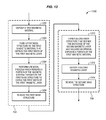
- FIG. 7 is a flow chart illustrating a method of fabricating the magnetic write head of FIGS. 5 and 6 in an exemplary embodiment.
- FIGS. 8 and 9 are cross-sectional and top views, respectively, illustrating the write head after forming the main write pole and a gap structure for the main write pole according to a step of the method of FIG. 7 .
- FIGS. 10 and 11 are cross-sectional and top views, respectively, illustrating the write head after forming a first magnetic layer for a wrap around shield according to a step of the method of FIG. 7 .
- FIG. 12 is a top view illustrating the write head after forming a second magnetic layer for the wrap around shield according to a step of the method of FIG. 7 .
- FIG. 13 is a flow chart illustrating additional steps for the method of FIG. 7 in an exemplary embodiment.
- FIGS. 14 and 15 are cross-sectional and top views, respectively, illustrating the write head after depositing a first magnetic material for the wrap around shield according to a step of the method of FIG. 13 .
- FIGS. 16 and 17 are cross-sectional and top views, respectively, illustrating the write head after forming a first mask structure on the first magnetic material that defines a width of the first magnetic layer according to a step of the method of FIG. 13 .
- FIGS. 18 and 19 are cross-sectional and top views, respectively, illustrating the write head after performing a removal process which removes portions of the magnetic material exposed by the first mask structure to define the width of the first magnetic layer according to a step of the method of FIG. 13 .
- FIGS. 20 and 21 are cross-sectional and top views, respectively, illustrating the write head after removing the first mask structure according to a step of the method of FIG. 13 .
- FIGS. 22 and 23 are cross-sectional and top views, respectively, illustrating the write head after forming a second mask structure that defines the back edge of the second magnetic layer and includes an opening exposing a portion of the first magnetic material according to a step of the method of FIG. 13 .
- FIGS. 24 and 25 are cross-sectional and top views, respectively, illustrating the write head after depositing a second magnetic layer for the wrap around shield according to a step of the method of FIG. 13 .
- FIG. 26 is a top view after removing the second mask structure according to a step of the method of FIG. 13 .
- FIG. 27 is a flow chart illustrating another method of fabricating the magnetic write head of FIGS. 5 and 6 in an exemplary embodiment.
- FIG. 28 is a top view illustrating the write head after forming a first magnetic layer for the wrap around shield according to a step of the method of FIG. 27 .
- FIG. 29 is a top view illustrating the write head after forming a second magnetic layer for the wrap around shield according to a step of the method of FIG. 27 .
- FIG. 30 is a flow chart illustrating additional steps for the method of FIG. 27 in an exemplary embodiment.
- FIGS. 31 and 32 are cross-sectional and top views, respectively, illustrating the write head after depositing an insulating material according to a step of the method of FIG. 30 .
- FIGS. 33 and 34 are cross-sectional and top views, respectively, illustrating the write head after forming a first mask structure exposing a portion of the insulating material to define the width of the first magnetic layer according to a step of the method of FIG. 30 .
- FIGS. 35 and 36 are cross-sectional and top views, respectively, illustrating the write head after performing a removal process which removes portions of the insulating material exposed by the first mask structure according to a step of the method of FIG. 30 .
- FIGS. 37 and 38 are cross-sectional and top views, respectively, illustrating the write head after removing the first mask structure according to a step of the method of FIG. 30 .
- FIGS. 39 and 40 are cross-sectional and top views, respectively, illustrating the write head after forming a second mask structure that defines the back edges of the first and the second magnetic layers and includes an opening for a wrap around shield according to a step of the method of FIG. 30 .
- FIGS. 41 and 42 are cross-sectional and top views, respectively, illustrating the write head after depositing a first magnetic material for the wrap around shield according to a step of the method of FIG. 30 .
- FIGS. 43 and 44 are cross-sectional and top views, respectively, illustrating the write head after performing a removal process which removes portions of the insulating material exposed by the second mask structure according to a step of the method of FIG. 30 .
- FIGS. 45 and 46 are cross-sectional and top views, respectively, illustrating the write head after depositing a second magnetic material for the wrap around shield according to a step of the method of FIG. 30 .
- FIG. 1 illustrates a typical magnetic disk drive system 100 .
- Magnetic disk drive system 100 includes a spindle 102 , a magnetic recording disk 104 , a motor controller 106 , an actuator 108 , an actuator/suspension arm 110 , and a slider 114 .
- Spindle 102 supports and rotates magnetic recording disk 104 in the direction indicated by the arrow.
- a spindle motor (not shown) rotates spindle 102 according to control signals from motor controller 106 .
- Slider 114 is supported by actuator/suspension arm 110 .
- Actuator/suspension arm 110 is connected to actuator 108 that moves in order to position slider 114 over a desired track of magnetic recording disk 104 .
- Magnetic disk drive system 100 may include other devices, components, or systems not shown in FIG. 1 . For instance, a plurality of magnetic disks, actuators, actuator/suspension arms, and sliders may be used.
- ABS air bearing surface
- FIG. 2 illustrates a typical slider 114 .
- the view of slider 114 is of the ABS side of slider 114 , which is the surface of the page in FIG. 2 .
- Slider 114 has a cross rail 202 , two side rails 204 - 205 , and a center rail 206 on the ABS side.
- the rails on slider 114 illustrate just one embodiment, and the configuration of the ABS side of slider 114 may take on any desired form.
- Slider 114 also includes a write head 210 and a read head 212 on a trailing edge 214 of slider 114 .
- FIG. 3 is a cross-sectional view of a typical write head 210 .
- This view of write head 210 illustrates some of the layers that form write head 210 .
- Write head 210 includes a return pole 304 that is formed on a non-magnetic layer 302 .
- Non-magnetic layer 302 is generally a layer between write head 210 and read head 212 (not shown in this view).
- Write head 210 further includes a main write pole 308 (or main pole).
- Main write pole 308 is comprised of a yoke portion (not visible in this view) and a pole tip (also not visible in this view).
- the pole tip is located proximate to an ABS 316 of recording head 114 and extends inward from ABS 316 to connect with the yoke portion of main write pole 308 .
- Main write pole 308 and return pole 304 are connected to each other through a back gap layer 306 .
- An inductive coil 310 is sandwiched within an insulation layer 312 between the poles 304 and 308 .
- the rest of coil 310 is not shown in this view as it extends further back (i.e., to the right in this view) in write head 210 , although coil 310 may wrap around return pole 304 or main write pole 308 as a matter of design choice.
- Write head 210 may include other layers not shown, and may take on other configurations in other embodiments. For instance, a trailing shield or a wrap around shield may be formed around the pole tip to reduce cross-track interference when writing data using write head 210 .
- FIG. 4 is a cross-sectional view illustrating typical write head 210 including a bi-layer wrap around shield 408 having equal shield layer widths.
- shield 408 includes an inner layer 402 and an outer layer 404 .
- Inner layer 402 is proximate to main write pole 308 along pole tip 314 .
- Both inner layer 402 and outer layer 404 have a width 406 which is equal.
- shield 408 may include inner layer 402 (proximate to the write pole) and outer layer 404 (on the inner layer) to increase the write field gradient of write head 210 . Problems arise during fabrication when inner layer 402 protrudes above the ABS of write head 210 along width 406 of shield 408 . The protrusion presents a large potential contact area for slider 114 and reduces the clearance for slider 114 along this area.
- FIGS. 5 and 6 are cross-sectional and top views, respectively, illustrating a write head 522 including a bi-layer wrap around shield 520 having a narrow first layer 510 width 512 and coplanar back edge 602 in an exemplary embodiment.
- the cross-sectional view of write head 522 ( FIG. 5 ) is taken along plane A of an ABS 606 (see FIG. 6 for an indication of ABS 606 ).
- ABS 606 indicates a future ABS for write head 522 after performing a lapping process. In FIG. 6 , this lapping process would remove material from left to right until ABS 606 is reached. Referring to FIG.
- write head 522 includes a main write pole 504 , a gap structure 506 and 508 , and a wrap around shield 520 for main write pole 504 fabricated on a non-magnetic layer 502 (e.g., alumina).
- a first width 512 of first layer 510 for wrap around shield 520 is less than a second width 514 of a second layer 511 for wrap around shield 520 . Because first width 512 of first layer 510 is less than second width 514 of second layer 511 , first layer 510 protrudes from the ABS of write head 522 along a much smaller potential contact area than write head 210 .
- the inner layer 402 of shield 408 may protrude along the width 406 of shield 408 after a lapping process is performed to define ABS 316 (see FIG. 3 ).
- this protrusion may be substantial.
- second layer 511 may have second width 514 of about fifty microns.
- first layer 510 may have first width 512 of between about two to four microns.
- gap structure 506 and 508 surrounds main write pole 504 and includes a side gap (element 508 ) and a top gap (element 506 ).
- First layer 510 is proximate to main write pole 504 and may have a thickness 516 of between about thirty and two hundred nanometers.
- second layer 511 may have a thickness 518 of between about two and three microns.
- first layer 510 is thinner than second layer 511 and also narrower in width than second layer 511 .
- FIG. 6 illustrates an important design parameter for write head 522 , which is a throat height 604 for wrap around shield 520 .
- Throat height 604 is defined by a distance between ABS 606 of write head 522 and a back edge 602 for wrap around shield 520 . While first layer 510 and second layer 511 may have different widths 512 and 514 , back edge 602 for first layer 510 and second layer 511 are coplanar. This ensures that throat height 604 for wrap around shield 520 is fabricated accurately. How back edge 602 for first layer 510 and second layer 511 are defined will become more readily apparent in the subsequent discussions on the fabrication of write head 522 .
- dashed lines are drawn in the top view of write head 522 .
- the dashed lines indicate features underneath various layers of materials fabricated for write head 522 .
- FIG. 6 shows a dashed outline for main write pole 504 .
- main write pole 504 is underneath top gap 506 and surrounded by side gap 508 .
- Dashed lines for first layer 510 in this view also illustrate that second layer 511 is fabricated on first layer 510 .
- the dashed lines allow for various features of write head 522 to be discussed even though such features may be hidden by other layers for write head 522 .
- FIG. 7 is a flow chart illustrating a method 700 of fabricating magnetic write head 522 of FIGS. 5 and 6 in an exemplary embodiment.
- the steps of the flow charts provided herein are not all inclusive and other steps, not shown, may be included. Further, the steps may be performed in an alternative order.
- write head 522 may be fabricated on a number of pre-existing layers of a wafer, such as layers forming a read head. While the following discussion details the fabrication of one write head 522 on a wafer, one skilled in the art understands that fabricating write heads is a wafer level fabrication process, and therefore hundreds or even thousands of write heads may be fabricated simultaneously.
- Step 702 of FIG. 7 comprises forming main write pole 504 and gap structure 506 and 508 for main write pole 504 .
- FIGS. 8 and 9 are cross-sectional and top views, respectively, illustrating write head 522 after forming main write pole 504 and gap structure 506 and 508 .
- main write pole 504 and gap structure 506 and 508 When forming main write pole 504 and gap structure 506 and 508 , one skilled in the art understands that a number of fabrication steps have been omitted for brevity in arriving at the resulting FIGS. 8 and 9 .
- Such omitted steps may include depositing magnetic material (e.g., NiFe, CoFe, etc.) for main write pole 504 , forming one or more mask structures for defining main write pole 504 , performing a milling process to remove magnetic material and to define main write pole 504 , etc. Additional steps may include depositing gap material (e.g., alumina) for a side gap and a top gap to form gap structure 506 and 508 .
- magnetic material e.g., NiFe, CoFe, etc.
- Additional steps may include depositing gap material (e.g., alumina) for a side gap and a top gap to form gap structure 506 and 508 .
- Step 704 of FIG. 7 comprises forming first layer 510 for wrap around shield 520 (see FIG. 5 ).
- FIGS. 10 and 11 are cross-sectional and top views, respectively, illustrating write head 522 after forming first layer 510 .
- FIG. 11 illustrates the relative location of first layer 510 with respect to ABS 606 and back edge 602 . More particularly, FIG. 11 illustrates how first layer 510 , when formed, extends to the right of back edge 602 . How the placement of first layer 510 will be used to form a back edge for first layer 510 will become more apparent in subsequent fabrication steps and the related discussion below.
- FIG. 10 and 11 are cross-sectional and top views, respectively, illustrating write head 522 after forming first layer 510 .
- FIG. 11 illustrates the relative location of first layer 510 with respect to ABS 606 and back edge 602 . More particularly, FIG. 11 illustrates how first layer 510 , when formed, extends to the right of back edge 602 . How the placement of first layer 510
- first layer 510 is formed around the pole tip for main write pole 504 , and is isolated from write pole 504 by gap structure 506 and 508 .
- Forming first layer 510 may include electroplating or sputter depositing a high magnetic moment CoFeNi magnetic material to a thickness 516 of between about thirty nanometers and one hundred nanometers. Further, forming first layer 510 may include a number of depositing, masking, and etching steps not shown.
- Step 706 of FIG. 7 comprises forming second layer 511 on first layer 510 for wrap around shield 520 , where first width 512 of first layer 510 is less than second width 514 (see FIG. 5 ) of second layer 511 .
- FIG. 12 is a top view illustrating write head 522 after forming second layer 511 for wrap around shield 520 .
- second layer 511 covers first layer 510 (as indicated for the dashed lines for first layer 510 ) up to a back edge for second layer 511 as shown along the line for back edge 602 . Note that a portion of first layer 510 remains exposed in FIG. 12 by second layer 511 .
- Forming second layer 511 may include electroplating or sputter depositing a lower magnetic moment (relative to the magnetic moment of first layer 510 ) CoFeNi material to a thickness 518 of between about two and three microns. Further, forming second layer 511 may include a number of depositing, masking, and etching steps not shown.
- Step 708 of FIG. 7 comprises performing a removal process which removes portions of first layer 510 exposed by second layer 511 to define back edge 602 of first layer 510 and second layer 511 that are coplanar.
- a removal process e.g., ion milling
- second layer 511 forms a mask protecting first layer 510 .
- back edge 602 for first layer 510 and second layer 511 are defined such that they are coplanar. This allows for a desired throat height 604 for wrap around shield 520 .
- FIGS. 5 and 6 are the result of performing step 708 .
- FIG. 13 is a flow chart illustrating additional steps for method 700 of FIG. 7 in an exemplary embodiment. More particularly, the flow chart of FIG. 13 will illustrate additional details for step 704 of method 700 (forming first layer 510 , as shown in steps 1302 - 1308 of FIG. 13 ) and additional details for step 706 of method 700 (forming second layer 511 , as shown in steps 1310 - 1314 of FIG. 13 ).
- Step 1302 of FIG. 13 comprises depositing a first magnetic material for wrap around shield 520 .
- a Ta/Ru seed layer may be deposited to a thickness of between about twenty and thirty nanometers.
- FIGS. 14 and 15 are cross-sectional and top views, respectively, illustrating write head 522 after depositing a first magnetic material 1402 for wrap around shield 520 .
- the top view of write head 522 shown in FIG. 15 illustrates that first magnetic material 1402 is a full film deposition process.
- First magnetic material 1402 e.g., CoFeNi
- Thickness 516 may be between about thirty nanometers and one hundred nanometers.
- Step 1304 of FIG. 13 comprises forming a first mask structure on first magnetic material 1402 that defines first width 512 of first layer 510 .
- FIGS. 16 and 17 are cross-sectional and top views, respectively, illustrating write head 522 after forming a first mask structure 1602 on first magnetic material 1402 that defines first width 512 of first layer 510 .
- First mask structure 1602 may include a hard mask (not shown), an image transfer mask (not shown), and a resist layer (not shown).
- first mask structure 1602 has already been photo patterned to define width 512 .
- the top view of FIG. 17 illustrates the placement of first mask structure 1602 relative to back edge 602 .
- Step 1306 of FIG. 13 comprises performing a removal process which removes a portion of magnetic material 1402 exposed by first mask structure 1602 to define first width 512 of first layer 510 (see FIG. 5 ).
- FIGS. 18 and 19 are cross-sectional and top views, respectively, illustrating write head 522 after performing a removal process which removes a portion of magnetic material 1402 exposed by first mask structure 1602 to define first width 512 of first layer 510 .
- Step 1308 of FIG. 13 comprises removing first mask structure 1602 .
- FIGS. 20 and 21 are cross-sectional and top views, respectively, illustrating write head 522 after removing first mask structure 1602 .
- first magnetic material 1402 may be re-capped with between about three and eight nanometers of CoFeNi material.
- Step 1310 of FIG. 13 comprises forming a second mask structure that defines a back edge of second magnetic layer 511 and includes an opening exposing a portion of first magnetic material 1402 .
- FIGS. 22 and 23 are cross-sectional and top views, respectively, illustrating write head 522 after forming a second mask structure 2202 that defines a back edge (disposed along back edge 602 ) of a second magnetic material and includes an opening 2302 exposing a portion of first magnetic material 1402 .
- Second mask structure 2202 may include a hard mask (not shown), an image transfer mask (not shown), and a resist layer (not shown).
- second mask structure 2202 has already been photo patterned to define opening 2302 . Opening 2302 will define second width 514 of second layer 511 .
- the top view of FIG. 23 illustrates how second mask structure 2202 covers most of the material of write head 522 in this step, with the exception of material exposed by opening 2302 . Some of the material exposed by opening 2302 includes first magnetic material 1402 .
- Step 1312 of FIG. 13 comprises depositing a second magnetic material for wrap around shield 520 .
- FIGS. 24 and 25 are cross-sectional and top views, respectively, illustrating write head 522 after depositing a second magnetic material 2402 .
- Second magnetic material 2402 e.g., CoFeNi
- Second magnetic material 2402 may be deposited by an electroplating process to cover material exposed by opening 2302 .
- Second magnetic material 2402 may also cover second mask structure 2202 , but this has been omitted for the sake of clarity.
- Second magnetic material 2402 may be deposited to thickness 518 of between about two and three microns. Further, the top view of FIG.
- second magnetic material 2402 covers a majority of first magnetic material 1402 and exposes a portion of first magnetic material 1402 to the right of back edge 602 .
- a back edge of first magnetic material 1402 and a back edge of second magnetic material 2402 are not as yet coplanar.
- Step 1314 of FIG. 13 comprises removing second mask structure 3302 .
- second magnetic material 2402 attached to second mask structure 2202 will also be removed.
- FIG. 26 is a top view illustrating write head 522 after removing second mask structure 2202 .
- step 708 of method 700 is performed.
- a portion of first magnetic material 1402 exposed by second magnetic material 2402 is removed to define back edge 602 for first magnetic material 1402 and second magnetic material 511 such that they are coplanar.
- FIGS. 5 and 6 are the result of performing step 708 of method 700 ; first magnetic material 1402 and second magnetic material 2402 are first layer 510 and second layer 511 , respectively.
- FIG. 27 is a flow chart illustrating another method 2700 of fabricating write head 522 of FIGS. 5 and 6 in an exemplary embodiment.
- first and second layers 510 - 511 were first fabricated to overlap and then second layer 511 was used as a mask during a removal process to create coplanar back edge 602 .
- Method 2700 will illustrate an alternate fabrication process whereby first and second layers 510 - 511 will formed in place as coplanar layers.
- Step 2702 of FIG. 27 comprises forming main write pole 504 and gap structure 506 and 508 for main write pole 504 .
- This step may be substantially similar to step 702 of method 700 and therefore will not be re-iterated here.
- Step 2704 of FIG. 27 comprises forming first layer 510 .
- FIG. 28 is a top view illustrating write head 522 after forming first layer. Note that the top view of FIG. 28 illustrates that first layer 510 is deposited to align with back edge 602 . This is in contrast to FIG. 12 , which illustrates that first layer 510 was formed to be offset across back edge 602 as compared to second layer 511 .
- Step 2706 of FIG. 27 comprises forming second layer 511 on first layer 510 for wrap around shield 520 .
- FIG. 29 illustrate write head 522 after forming second layer 511 . Note that in contrast to method 700 , a removal process is not performed to generate back edge 602 that is coplanar for first and second layers 510 - 511 . Instead, first and second layers 510 - 511 are formed in place as coplanar.
- FIG. 5 illustrates a cross-sectional view of the result of performing step 1706 .
- FIG. 30 is a flow chart illustrating additional steps for method 2700 of FIG. 27 in an exemplary embodiment. More particularly, the flow chart of FIG. 30 illustrates additional details for step 2704 of method 2700 (forming first layer 510 , as shown in steps 3002 - 3012 of FIG. 30 ) and additional details for step 2706 of method 2700 (forming second layer 511 , as shown in steps 3014 - 3018 of FIG. 30 ).
- Step 3002 of FIG. 30 comprises depositing an insulating material. Prior to depositing the insulating material, a Ta/Ru seed layer may be deposited.
- FIGS. 31 and 32 are cross-sectional and top views, respectively, illustrating write head 522 after depositing an insulating material 3102 .
- Insulating material 3102 may be alumina, and is deposited full film. The thickness of insulating material 3102 may be about twenty five nanometers. Thus, insulating material 3102 covers gap structure 506 and 508 , and also covers non-magnetic layer 502 . This is illustrated in FIG. 32 , which shows dashed lines for the structures covered by insulating material 3102 .
- Step 3004 of FIG. 30 comprises forming a first mask structure exposing a portion of insulating material 3102 to define first width 512 of first layer 510 .
- FIGS. 33 and 34 are cross-sectional and top views, respectively, illustrating write head 522 after forming a first mask structure 3202 exposing a portion of insulating material 3102 to define first width 512 of the first layer 510 .
- First mask structure 3302 covers a majority of insulating material 3102 with the exception of a portion proximate to write pole 504 exposed by opening 3402 .
- First mask structure 3302 may include a hard mask (not shown), an image transfer mask (not shown), and a resist layer (not shown). In FIGS. 33 and 34 , first mask structure 3302 has already been photo patterned to define opening 3402 .
- Step 3006 of FIG. 30 comprises performing a removal process which removes a portion of insulating material 3102 exposed by first mask structure 3302 .
- FIGS. 35 and 36 are cross-sectional and top views, respectively, illustrating write head 522 after performing a removal process which removes a portion of insulating material 3102 exposed by first mask structure 3302 . Note that FIG. 35 illustrates that non-magnetic layer 502 is exposed along first width 512 proximate to write pole 504 .
- Step 3008 of FIG. 30 comprises removing first mask structure 3302 .
- FIGS. 37 and 38 are cross-sectional and top views, respectively, illustrating write head 522 after removing first mask structure 3302 .
- Step 3010 of FIG. 30 comprises forming a second mask structure that defines back edge 602 of first and second layers 510 - 511 and includes an opening for wrap around shield 520 .
- FIGS. 39 and 40 are cross-sectional and top views, respectively, illustrating write head 522 after forming second mask structure 3902 that defines back edge 602 of first and second magnetic layers 510 - 511 and includes an opening 3402 for wrap around shield 520 according.
- Second mask structure 3902 may include a hard mask (not shown), an image transfer mask (not shown), and a resist layer (not shown).
- second mask structure 3902 has already been photo patterned to define opening 3402 .
- Opening 3402 exposes a portion of insulating material 3102 and non-magnetic layer 502 along second width 514 . Opening 3402 is also disposed along back edge 602 to allow for first and second layers 510 - 511 to be deposited in place as coplanar.
- Step 3012 of FIG. 30 comprises depositing a first magnetic material for wrap around shield 520 .
- FIGS. 41 and 42 are cross-sectional and top views, respectively, illustrating write head 522 after depositing first magnetic material 4102 for wrap around shield 520 .
- First magnetic material 4102 is deposited (e.g., by electroplating first magnetic material 4102 on portions of write head 522 not covered by second mask structure 3902 and insulating layer 3102 ) on gap structure 506 and 508 of main write pole 504 and non-magnetic layer 502 exposed by insulating material 3102 . Further, because second mask structure 3902 aligns with back edge 602 , a back edge of first magnetic material 4102 also aligns with back edge 602 .
- First magnetic material 4102 may be deposited to a thickness 516 of between about fifty and two hundred nanometers.
- Step 3014 of FIG. 30 comprises performing a removal process which removes a portion of insulating material 3102 exposed by second mask structure 3902 .
- FIGS. 43 and 44 are cross-sectional and top views, respectively, illustrating write head 522 after performing a removal process which removes a portion of insulating material 3102 exposed by second mask structure 3902 .
- opening 3402 of second mask structure 3902 illustrates how non-magnetic layer 502 is exposed by removing portions of insulating material 3102 .
- a photo-developer e.g., Tetramethylammonium Hydroxide or TMAH
- TMAH Tetramethylammonium Hydroxide
- a photo-developer may be used when more aggressive thin film etchants might damage second mask structure 3902 when attempting to remove portions of insulating material 3102 .
- the photo-developer used to remove insulating material 3102 may be the same developer used to pattern second mask structure 3902 .
- Step 3016 of FIG. 30 comprises depositing a second magnetic material for wrap around shield 520 .
- FIGS. 45 and 46 are cross-sectional and top views, respectively, illustrating write head 522 after depositing a second magnetic material 4502 .
- Second magnetic material 4502 may be deposited to thickness 518 of between about two and three microns. Referring to the top view illustrated in FIG. 46 , opening 3402 exposes non-magnetic layer 502 and first magnetic layer 4102 to the deposition process. Material is deposited within opening 3402 such that second magnetic material 4502 along back edge 602 is coplanar with first magnetic material 4102 . Second mask structure 3902 may then be removed. Insulation material 3102 exposed by removing second mask structure 3902 may also be removed. The resulting write head 522 is illustrated in FIGS. 5 and 6 , where first magnetic material 4102 and second magnetic material 4502 correspond with first layer 510 and second layer 511 , respectively.
Abstract
Description
Claims (8)
Priority Applications (1)
| Application Number | Priority Date | Filing Date | Title |
|---|---|---|---|
| US12/914,543 US8619391B2 (en) | 2010-10-28 | 2010-10-28 | Magnetic write heads with bi-layer wrap around shields having dissimilar shield layer widths |
Applications Claiming Priority (1)
| Application Number | Priority Date | Filing Date | Title |
|---|---|---|---|
| US12/914,543 US8619391B2 (en) | 2010-10-28 | 2010-10-28 | Magnetic write heads with bi-layer wrap around shields having dissimilar shield layer widths |
Publications (2)
| Publication Number | Publication Date |
|---|---|
| US20120106002A1 US20120106002A1 (en) | 2012-05-03 |
| US8619391B2 true US8619391B2 (en) | 2013-12-31 |
Family
ID=45996484
Family Applications (1)
| Application Number | Title | Priority Date | Filing Date |
|---|---|---|---|
| US12/914,543 Active 2031-06-19 US8619391B2 (en) | 2010-10-28 | 2010-10-28 | Magnetic write heads with bi-layer wrap around shields having dissimilar shield layer widths |
Country Status (1)
| Country | Link |
|---|---|
| US (1) | US8619391B2 (en) |
Cited By (1)
| Publication number | Priority date | Publication date | Assignee | Title |
|---|---|---|---|---|
| US20150029615A1 (en) * | 2013-07-24 | 2015-01-29 | HGST Netherlands B.V. | Magnetic Write Head Having A Recessed High Moment Portion Of The Wrap-Around Shield |
Families Citing this family (1)
| Publication number | Priority date | Publication date | Assignee | Title |
|---|---|---|---|---|
| US9230566B1 (en) * | 2014-10-29 | 2016-01-05 | HGST Netherlands B.V. | Perpendicular magnetic write head having a controlled magnetization state shield |
Citations (17)
| Publication number | Priority date | Publication date | Assignee | Title |
|---|---|---|---|---|
| US20050141137A1 (en) | 2003-12-24 | 2005-06-30 | Hitachi Global Storage Technologies Netherlands, B.V. | Magnetic recording head for perpendicular recording, fabrication process, and magnetic disk storage apparatus mounting the magnetic head |
| US7009812B2 (en) | 2003-09-29 | 2006-03-07 | Hitachi Global Storage Technologies Netherlands B.V. | Magnetic transducer for perpendicular magnetic recording with single pole write head with trailing shield |
| US20070146929A1 (en) | 2005-11-02 | 2007-06-28 | Hitachi Global Storage Technologies Netherlands B.V. | Perpendicular head with the shield which approaches through the continuous non-magnetic film to the flare point of the main pole |
| US7239478B1 (en) * | 2004-01-31 | 2007-07-03 | Western Digital (Fremont), Inc. | Write element for perpendicular recording in a data storage system |
| US7379276B2 (en) | 2003-09-19 | 2008-05-27 | Samsung Electronics Co., Ltd. | Magnetic recording head having a plurality of shield layers |
| US7394620B2 (en) | 2003-04-28 | 2008-07-01 | Kabushiki Kaisha Toshiba | Perpendicular magnetic recording head and magnetic disc apparatus |
| US7392577B2 (en) | 2003-09-12 | 2008-07-01 | Tdk Corporation | Method for manufacturing a perpendicular magnetic head |
| US20090002895A1 (en) | 2007-06-26 | 2009-01-01 | Seagate Technology Llc | Wire-assisted magnetic write device with a gapped trailing shield |
| US20090154026A1 (en) * | 2007-12-12 | 2009-06-18 | Ming Jiang | Method for manufacturing a perpendicular magnetic write head with a thin wrap around magnetic shield |
| US20090168240A1 (en) * | 2007-12-28 | 2009-07-02 | Wen-Chien David Hsiao | Perpendicular write head having a modified wrap-around shield to improve overwrite, adjacent track interference and magnetic core width dependence on skew angle |
| JP2009259365A (en) | 2008-04-21 | 2009-11-05 | Hitachi Global Storage Technologies Netherlands Bv | Perpendicular magnetic recording head |
| US7633714B2 (en) | 2006-07-26 | 2009-12-15 | Headway Technologies, Inc. | Magnetic head for perpendicular magnetic recording and method of manufacturing same |
| KR20100044818A (en) | 2007-07-05 | 2010-04-30 | 지티이 코포레이션 | Random access method of time division synchronization code division mulitple access enhanced uplink system |
| US20100302688A1 (en) * | 2009-05-26 | 2010-12-02 | Masato Shiimoto | Magnetoresistive Effect Head and Magnetic Recording/Playback Device |
| US20100328816A1 (en) * | 2007-04-13 | 2010-12-30 | Headway Technologies, Inc. | Composite shield structure of PMR writer for high track density |
| US20110222188A1 (en) * | 2010-03-15 | 2011-09-15 | Hitachi, Ltd. | Perpendicular recording magnetic head, manufacturing method thereof and magnetic disk drive |
| US20110261485A1 (en) * | 2010-04-23 | 2011-10-27 | Aron Pentek | Magnetic write head having a wrap around trailing shield with an asymetrical side gap |
-
2010
- 2010-10-28 US US12/914,543 patent/US8619391B2/en active Active
Patent Citations (19)
| Publication number | Priority date | Publication date | Assignee | Title |
|---|---|---|---|---|
| US7394620B2 (en) | 2003-04-28 | 2008-07-01 | Kabushiki Kaisha Toshiba | Perpendicular magnetic recording head and magnetic disc apparatus |
| US7392577B2 (en) | 2003-09-12 | 2008-07-01 | Tdk Corporation | Method for manufacturing a perpendicular magnetic head |
| US7379276B2 (en) | 2003-09-19 | 2008-05-27 | Samsung Electronics Co., Ltd. | Magnetic recording head having a plurality of shield layers |
| US7009812B2 (en) | 2003-09-29 | 2006-03-07 | Hitachi Global Storage Technologies Netherlands B.V. | Magnetic transducer for perpendicular magnetic recording with single pole write head with trailing shield |
| US20050141137A1 (en) | 2003-12-24 | 2005-06-30 | Hitachi Global Storage Technologies Netherlands, B.V. | Magnetic recording head for perpendicular recording, fabrication process, and magnetic disk storage apparatus mounting the magnetic head |
| US7239478B1 (en) * | 2004-01-31 | 2007-07-03 | Western Digital (Fremont), Inc. | Write element for perpendicular recording in a data storage system |
| US20070146929A1 (en) | 2005-11-02 | 2007-06-28 | Hitachi Global Storage Technologies Netherlands B.V. | Perpendicular head with the shield which approaches through the continuous non-magnetic film to the flare point of the main pole |
| US7633714B2 (en) | 2006-07-26 | 2009-12-15 | Headway Technologies, Inc. | Magnetic head for perpendicular magnetic recording and method of manufacturing same |
| US20100328816A1 (en) * | 2007-04-13 | 2010-12-30 | Headway Technologies, Inc. | Composite shield structure of PMR writer for high track density |
| US20090002895A1 (en) | 2007-06-26 | 2009-01-01 | Seagate Technology Llc | Wire-assisted magnetic write device with a gapped trailing shield |
| KR20100044818A (en) | 2007-07-05 | 2010-04-30 | 지티이 코포레이션 | Random access method of time division synchronization code division mulitple access enhanced uplink system |
| US20090154026A1 (en) * | 2007-12-12 | 2009-06-18 | Ming Jiang | Method for manufacturing a perpendicular magnetic write head with a thin wrap around magnetic shield |
| US8000059B2 (en) * | 2007-12-12 | 2011-08-16 | Hitachi Global Storage Technologies Netherlands B.V. | Perpendicular magnetic write head with a thin wrap around magnetic shield |
| US20090168240A1 (en) * | 2007-12-28 | 2009-07-02 | Wen-Chien David Hsiao | Perpendicular write head having a modified wrap-around shield to improve overwrite, adjacent track interference and magnetic core width dependence on skew angle |
| US8120874B2 (en) * | 2007-12-28 | 2012-02-21 | Hitachi Global Storage Technologies Netherlands B.V. | Perpendicular write head having a modified wrap-around shield to improve overwrite, adjacent track interference and magnetic core width dependence on skew angle |
| JP2009259365A (en) | 2008-04-21 | 2009-11-05 | Hitachi Global Storage Technologies Netherlands Bv | Perpendicular magnetic recording head |
| US20100302688A1 (en) * | 2009-05-26 | 2010-12-02 | Masato Shiimoto | Magnetoresistive Effect Head and Magnetic Recording/Playback Device |
| US20110222188A1 (en) * | 2010-03-15 | 2011-09-15 | Hitachi, Ltd. | Perpendicular recording magnetic head, manufacturing method thereof and magnetic disk drive |
| US20110261485A1 (en) * | 2010-04-23 | 2011-10-27 | Aron Pentek | Magnetic write head having a wrap around trailing shield with an asymetrical side gap |
Cited By (2)
| Publication number | Priority date | Publication date | Assignee | Title |
|---|---|---|---|---|
| US20150029615A1 (en) * | 2013-07-24 | 2015-01-29 | HGST Netherlands B.V. | Magnetic Write Head Having A Recessed High Moment Portion Of The Wrap-Around Shield |
| US9036299B2 (en) * | 2013-07-24 | 2015-05-19 | HGST Netherlands B.V. | Magnetic write head having a recessed high moment portion of the wrap-around shield |
Also Published As
| Publication number | Publication date |
|---|---|
| US20120106002A1 (en) | 2012-05-03 |
Similar Documents
| Publication | Publication Date | Title |
|---|---|---|
| US7464458B2 (en) | Method for manufacturing a self-aligned, notched trailing shield for perpendicular recording | |
| US8051552B2 (en) | Stitched wrap around shield fabrication for perpendicular magnetic recording write heads | |
| US8259413B2 (en) | Write head with self-align layer and a method for making the same | |
| US8451560B2 (en) | Magnetic head with flared write pole with multiple non-magnetic layers thereover | |
| US7578049B2 (en) | Method for constructing a magnetic write pole for a perpendicular magnetic recording head | |
| US7648731B2 (en) | Fabricating perpendicular write elements in perpendicular magnetic recording heads | |
| US8035922B2 (en) | Write head with integrated coil and shield structure | |
| US7788798B2 (en) | Method for manufacturing a perpendicular magnetic write head with wrap around magnetic trailing and side shields | |
| US20130022840A1 (en) | Method for manufacturing a magnetic write head with a floating leading shield | |
| US8453317B2 (en) | Magnetic write head fabrication with integrated electrical lapping guides | |
| JPH117615A (en) | Manufacture of combined magnetic head | |
| US8619391B2 (en) | Magnetic write heads with bi-layer wrap around shields having dissimilar shield layer widths | |
| US9824700B1 (en) | Manufacturing method for a magnetic head including a main pole and a write shield | |
| US7765677B2 (en) | Method for manufacturing a magnetic write head using a protective layer to prevent write pole consumption | |
| US7372667B2 (en) | Thin-film magnetic head, head gimbal assembly with thin-film magnetic head, head arm assembly with head gimbal assembly, magnetic disk drive apparatus with head gimbal assembly and manufacturing method of thin-film magnetic head | |
| US10339964B1 (en) | Perpendicular magnetic recording (PMR) write head with patterned high moment trailing shield | |
| US8889018B2 (en) | Method for manufacturing a magnetic write pole using a multi-layered hard mask structure | |
| US8780499B2 (en) | Magnetic write head having a residual shield seed layer for reducing overwriting | |
| US8186040B2 (en) | Methods for creating slanted perpendicular magnetic pole via metal liftoff | |
| US8634161B2 (en) | Systems having writer with deeper wrap around shield and methods for making the same | |
| US9406323B2 (en) | Slider with aluminum compound fill | |
| US8028399B2 (en) | Magnetic write pole fabrication | |
| US8449752B2 (en) | Trailing plated step | |
| US8551347B2 (en) | Methods for creating a stepped perpendicular magnetic pole via milling and/or metal liftoff | |
| US8323517B2 (en) | Method of forming magnetic pole section of perpendicular magnetic recording type thin-film magnetic head and manufacturing method of perpendicular magnetic recording type thin-film magnetic head |
Legal Events
| Date | Code | Title | Description |
|---|---|---|---|
| AS | Assignment |
Owner name: HITACHI GLOBAL STORAGE TECHNOLOGIES NETHERLANDS B. Free format text: ASSIGNMENT OF ASSIGNORS INTEREST;ASSIGNORS:HSU, YIMIN;PENTEK, ARON;ROUCOUX, THOMAS;AND OTHERS;SIGNING DATES FROM 20101012 TO 20101027;REEL/FRAME:025214/0172 |
|
| AS | Assignment |
Owner name: HGST, NETHERLANDS B.V., NETHERLANDS Free format text: CHANGE OF NAME;ASSIGNOR:HGST, NETHERLANDS B.V.;REEL/FRAME:029341/0777 Effective date: 20120723 Owner name: HGST NETHERLANDS B.V., NETHERLANDS Free format text: CHANGE OF NAME;ASSIGNOR:HITACHI GLOBAL STORAGE TECHNOLOGIES NETHERLANDS B.V.;REEL/FRAME:029341/0777 Effective date: 20120723 |
|
| FEPP | Fee payment procedure |
Free format text: PAYOR NUMBER ASSIGNED (ORIGINAL EVENT CODE: ASPN); ENTITY STATUS OF PATENT OWNER: LARGE ENTITY |
|
| STCF | Information on status: patent grant |
Free format text: PATENTED CASE |
|
| AS | Assignment |
Owner name: WESTERN DIGITAL TECHNOLOGIES, INC., CALIFORNIA Free format text: ASSIGNMENT OF ASSIGNORS INTEREST;ASSIGNOR:HGST NETHERLANDS B.V.;REEL/FRAME:040826/0327 Effective date: 20160831 |
|
| FPAY | Fee payment |
Year of fee payment: 4 |
|
| AS | Assignment |
Owner name: JPMORGAN CHASE BANK, N.A., AS AGENT, ILLINOIS Free format text: SECURITY INTEREST;ASSIGNOR:WESTERN DIGITAL TECHNOLOGIES, INC.;REEL/FRAME:052915/0566 Effective date: 20200113 |
|
| MAFP | Maintenance fee payment |
Free format text: PAYMENT OF MAINTENANCE FEE, 8TH YEAR, LARGE ENTITY (ORIGINAL EVENT CODE: M1552); ENTITY STATUS OF PATENT OWNER: LARGE ENTITY Year of fee payment: 8 |
|
| AS | Assignment |
Owner name: WESTERN DIGITAL TECHNOLOGIES, INC., CALIFORNIA Free format text: RELEASE OF SECURITY INTEREST AT REEL 052915 FRAME 0566;ASSIGNOR:JPMORGAN CHASE BANK, N.A.;REEL/FRAME:059127/0001 Effective date: 20220203 |
|
| AS | Assignment |
Owner name: JPMORGAN CHASE BANK, N.A., ILLINOIS Free format text: PATENT COLLATERAL AGREEMENT - A&R LOAN AGREEMENT;ASSIGNOR:WESTERN DIGITAL TECHNOLOGIES, INC.;REEL/FRAME:064715/0001 Effective date: 20230818 Owner name: JPMORGAN CHASE BANK, N.A., ILLINOIS Free format text: PATENT COLLATERAL AGREEMENT - DDTL LOAN AGREEMENT;ASSIGNOR:WESTERN DIGITAL TECHNOLOGIES, INC.;REEL/FRAME:067045/0156 Effective date: 20230818 |