US7319730B2 - Data communication method and data communication device and semiconductor device - Google Patents
Data communication method and data communication device and semiconductor device Download PDFInfo
- Publication number
- US7319730B2 US7319730B2 US10/270,693 US27069302A US7319730B2 US 7319730 B2 US7319730 B2 US 7319730B2 US 27069302 A US27069302 A US 27069302A US 7319730 B2 US7319730 B2 US 7319730B2
- Authority
- US
- United States
- Prior art keywords
- data
- transmission
- reception
- signal
- bits
- Prior art date
- Legal status (The legal status is an assumption and is not a legal conclusion. Google has not performed a legal analysis and makes no representation as to the accuracy of the status listed.)
- Expired - Fee Related, expires
Links
Images


Classifications
-
- H—ELECTRICITY
- H04—ELECTRIC COMMUNICATION TECHNIQUE
- H04L—TRANSMISSION OF DIGITAL INFORMATION, e.g. TELEGRAPHIC COMMUNICATION
- H04L25/00—Baseband systems
- H04L25/02—Details ; arrangements for supplying electrical power along data transmission lines
- H04L25/14—Channel dividing arrangements, i.e. in which a single bit stream is divided between several baseband channels and reassembled at the receiver
-
- H—ELECTRICITY
- H04—ELECTRIC COMMUNICATION TECHNIQUE
- H04L—TRANSMISSION OF DIGITAL INFORMATION, e.g. TELEGRAPHIC COMMUNICATION
- H04L25/00—Baseband systems
- H04L25/38—Synchronous or start-stop systems, e.g. for Baudot code
- H04L25/40—Transmitting circuits; Receiving circuits
- H04L25/49—Transmitting circuits; Receiving circuits using code conversion at the transmitter; using predistortion; using insertion of idle bits for obtaining a desired frequency spectrum; using three or more amplitude levels ; Baseband coding techniques specific to data transmission systems
- H04L25/4906—Transmitting circuits; Receiving circuits using code conversion at the transmitter; using predistortion; using insertion of idle bits for obtaining a desired frequency spectrum; using three or more amplitude levels ; Baseband coding techniques specific to data transmission systems using binary codes
- H04L25/4908—Transmitting circuits; Receiving circuits using code conversion at the transmitter; using predistortion; using insertion of idle bits for obtaining a desired frequency spectrum; using three or more amplitude levels ; Baseband coding techniques specific to data transmission systems using binary codes using mBnB codes
-
- H—ELECTRICITY
- H04—ELECTRIC COMMUNICATION TECHNIQUE
- H04L—TRANSMISSION OF DIGITAL INFORMATION, e.g. TELEGRAPHIC COMMUNICATION
- H04L7/00—Arrangements for synchronising receiver with transmitter
- H04L7/02—Speed or phase control by the received code signals, the signals containing no special synchronisation information
- H04L7/033—Speed or phase control by the received code signals, the signals containing no special synchronisation information using the transitions of the received signal to control the phase of the synchronising-signal-generating means, e.g. using a phase-locked loop
Definitions
- the present invention relates to a data communication device and a technique effectively applied for a technique of data communication performed between, mainly, an MPU (Micro Processing Unit) and a main storage device or the like.
- MPU Micro Processing Unit
- Methods of performing data communication between integrated circuits are roughly divided into a parallel communication method (parallel link) using a plurality of transmission lines and transmitting data in parallel, and a serial communication method (serial link) using a single transmission line and transmitting data in series.
- the parallel link can simultaneously transmit plural data, so that a transmission/reception data amount per unit time is large.
- the parallel link is generally used, for example, in data communication between the semiconductor integrated circuits having a short transmission line.
- the serial link since only a piece of data can be transmitted/received per unit time, the transmission/reception data amount per unit time is small However, it is unnecessary to consider the timing skew, so that transmission of long distance is easy.
- the serial link is mainly used for connecting digital devices such as a VCR (video cassette recorder), a DVD player, a mini-disc recorder, a set-top box, and the like.
- MOS metal oxide semiconductor
- the data and clock signal CLK have jitter and skew, so that the phases vary.
- sufficient set-up time and hold time is necessary for data with respect to the clock signal CLK.
- the window of data as a timing margin is reduced by the jitter of the clock signal CLK and is further divided into the set-up time and hold time.
- the window of data is narrowed but the variations in the phases of the data and clock signal CLK do not change so much. It disturbs increase in the data transfer speed per transmission line in the parallel link.
- An input/output pin of a semiconductor integrated circuit device always includes an inductance component.
- a current does not pass to a CMOS buffer in a steady state but is generated only when transition takes place in a transmission line.
- the parallel link has a plurality of buffers.
- When transition takes place in output signals of all of the output buffers a large current flows between a power supply line in the chip and a ground line.
- the potential difference which appears between both ends of the inductance depends on a change amount of the flowing current and increases. Consequently, when the current largely changes as described above, the potential difference between the power supply line for applying an operation voltage to an output buffer and the ground line largely decreases on assumption that the external power supply line and the ground line are stable. Fluctuations between the power supply line and the ground line are called simultaneous switching noise.
- the power supply voltage decreases, the current driving force of the output buffer decreases, and a delay of the output buffer increases.
- a difference in delay time of the output buffer occurs between the case where the number of output signals in which transition occurs is large and the case where the number is small.
- the jitter causes decrease in the timing window, and it disturbs increase in the transmission speed.
- the larger the number of transmission lines is the larger the jitter in the transmission lines due to the simultaneous switching noise is, and increase in the number of transmission lines can be also prevented.
- a data communication method includes: a step of encoding data of N bits (N being 2 or larger) to transmission data of M bits (M being 3 or larger) on a transmission side; a step of generating a transmission signal in which transition takes place in at least one level of any of the transmission data synchronously with a transmission clock and transmitting the transmission signal to a transmission line on the transmission side; a step of recognizing transition in the signal of M bits received via the transmission line and detecting the reception data of M bits synchronized with the transmission clock on a reception side; and a step of decoding the reception data of M bits to the data of N bits.
- FIG. 1 is a block diagram showing an embodiment of a data communication device according to the invention.
- FIG. 2 is an operation waveform chart for explaining an example of the operation of the circuit of FIG. 1 .
- FIG. 3 is a configuration diagram showing an example of data encoding according to the invention.
- FIG. 4 is a circuit diagram showing an example of an encoder used for the invention.
- FIG. 5 is a circuit diagram showing an example of a decoder used for the invention.
- FIGS. 6A to 6C are waveform diagrams for explaining the invention.
- FIG. 7 is a schematic diagram of an equivalent circuit showing an example of transmission buffers and a package used for the invention.
- FIG. 8 is a waveform chart for explaining the operation of the equivalent circuit of FIG. 7 .
- FIG. 9 is a block diagram showing another example of the data communication device according to the invention.
- FIG. 10 is a timing chart for explaining the example of FIG. 9 .
- FIG. 11 is a circuit diagram showing an example of a parallel-to-serial converter in FIG. 9 .
- FIG. 12 is a block diagram showing another example of the data communication device according to the invention.
- FIG. 13 is a block diagram showing an example of a data sampling circuit of FIG. 12 .
- FIG. 14 is a timing chart for explaining an example of the operation of the data sampling circuit of FIG. 13 .
- FIG. 15 is a block diagram showing an example of a decoder in FIG. 12 .
- FIG. 16 is a waveform chart showing the relation between a sampling clock and a jitter of a transmission line in the example of FIG. 12 .
- FIG. 17 is an explanatory diagram showing the relation between the sampling clock in the example of FIG. 12 and transition probability of a transmission line.
- FIG. 18 is a timing chart for explaining an example of the operation of the data communication device of FIG. 12 .
- FIG. 19 is a block diagram showing another example of a reception circuit used for the invention.
- FIG. 20 is a circuit diagram showing an example of a 3-bit detection circuit used for the invention.
- FIG. 21 is a circuit diagram showing another example of the 3-bit detection circuit used for the invention.
- FIG. 22 is a timing chart for explaining an example of the operation of the example of FIG. 19 .
- FIG. 23 is a block diagram showing another example of the reception circuit used for the invention.
- FIG. 24 is a timing chart for explaining the operation of the example of FIG. 23 .
- FIG. 25 is a block diagram showing another example of the reception circuit used for the invention.
- FIG. 26 is a timing chart for explaining an example of the operation of the example of FIG. 25 .
- FIG. 27 is a block diagram showing an example of the data communication device according to the invention.
- FIG. 28 is a block diagram showing another example of the data communication device according to the invention.
- FIG. 1 is a block diagram showing an embodiment of a data communication device according to the invention.
- the schematic configuration of the data communication device of the embodiment is as follows.
- Reference numeral 110 denotes a transmission-side device
- reference numeral 120 indicates a reception-side device.
- each of the transmission-side device 110 and the reception-side device 120 is formed as a semiconductor chip.
- the two semiconductor chips 110 and 120 are connected to each other via transmission lines 110 _ 0 to 110 _ 5 .
- the transmission lines 110 _ 0 to 110 _ 5 are formed by printed wiring on a mounting board on which the transmission-side device 110 and the reception-side device 120 are mounted.
- terminals 116 _ 0 to 116 _ 3 are data input terminals to which transmission data generated by a not-illustrated data processing circuit included in the transmission-side device 110 is input.
- the embodiment is directed to an example of transmitting parallel data of four bits corresponding to the terminals 116 _ 0 to 116 _ 3 .
- the 4-bit data is converted to transition codes 117 _ 0 to 117 _ 5 of six bits by an encoder 111 .
- the transition codes 117 _ 0 to 117 _ 5 are transmitted to the transmission lines 101 _ 0 to 101 _ 5 via a transmission circuit.
- the transmission circuit converts the logic value of the transition code to a form indicative of the presence or absence of transition in the level of a transmission line by D-type flip-flops 112 _ 0 to 112 _ 5 and 113 _ 0 to 113 _ 5 which operate synchronously with a clock signal 118 for transmission and exclusive OR circuits 114 and transmits the resultant to the transmission lines 101 _ 0 to 101 _ 5 via an output buffer 115 .
- the level of the transmission line is shifted.
- the level of the transmission line is not shifted but is maintained.
- an exclusive OR circuit is used.
- the transition code is output from each of the D-type flip-flops 112 _ 0 to 112 _ 5 , and each of the flip-flops 113 _ 0 to 113 _ 5 maintains the immediately preceding level of the transmission line which is generated by the exclusive OR circuit 114 .
- the exclusive OR circuit 114 shifts (inverts) the level of the immediately preceding transmission line held in the flip-flops 113 _ 0 to 113 _ 5 .
- the exclusive OR circuit 114 outputs the level of the transmission line which is the same as that held in the flip-flops 113 _ 0 to 113 _ 5 .
- the level of the transmission line transmitted via each of the transmission lines 101 _ 0 to 101 _ 5 is received by an input buffer 125 , and a reception signal of the form indicative of the presence or absence of transition in the level of the transmission line is converted into each of binary transition codes 127 _ 0 to 127 _ 5 by a reception circuit constructed by flip-flops 123 _ 0 to 123 _ 5 and exclusive OR circuits 124 .
- the transition codes 127 _ 0 to 127 _ 5 are decoded to the original 4-bit data by a decoder 121 , the original 4-bit data is received by flip-flops 122 _ 0 to 122 _ 3 , and 4-bit reception data 126 _ 0 to 126 _ 3 is generated.
- the reception data is transmitted to a not-shown signal processing circuit.
- the encoder 111 when transmission data of the transmission-side device 110 consists of N bits, the encoder 111 encodes the N-bit transmission data into a transition code of M bits.
- setting is made so as to satisfy the relation of M>N, and the transition code obtained by the encoding includes logic 1 of at least one bit.
- FIG. 2 is an operation waveform chart for explaining an example of the operation of the circuit of the example shown in FIG. 1 .
- Description will be given on assumption that outputs of all of the D-type flip-flops (D-FF) in FIG. 1 are “0” in the initial state.
- D-FF D-type flip-flops
- each of the D-FFs is reset. Therefore, just before start of data communication, all of the D-FFs are reset.
- the timing of finishing the data communication may be instructed by a command, determined by predetermining an amount of data per communication command, or the like.
- the invention is not limited to the methods.
- a cycle of data transfer is defined as tCK.
- the operation of the transmission-side device 110 is as follows. Transmission data D(t)[3:0] generated by a not-shown signal processing circuit is input to the data input terminals 116 _ 0 to 116 _ 3 . D(t)[0], D(t)[1], D(t)[2], and D(t)[3] are input to the input terminals 116 _ 0 , 116 _ 1 , 116 _ 2 , and 116 _ 3 , respectively.
- an expression such as “D(t)[n] is input to 116 _n” will be used.
- D(t)[3:0] denotes data of time t and a bit width of four bits.
- the value of D(t)[3:0] becomes a discrete value by the transmission clock 118 , and data after one cycle of the transmission clock 118 is expressed as D(t+1)[3:0].
- the other data will be similarly described by the data expressing method.
- the data D(t)[3:0] is encoded by the encoder 111 and is output as a transition code T(t)[5:0] to the transmission line 117 _m.
- FIG. 3 is a configuration diagram showing an example of data encoding.
- the diagram shows an example of conversion by the encoding from D(t)[3:0] to T(t)[5:0].
- d(t)[3:0] and T(t)[5:0] correspond to each other in a one-to-one manner and can be converted mutually.
- the encoder 111 in FIG. 1 can be realized by using a read only memory (ROM). It can be also realized by combining logic gate circuits as will be described hereinbelow.
- FIG. 4 is a circuit diagram showing an example of an encoder used for the invention.
- parallel data of four bits supplied from the input terminals 116 _ 0 to 116 _ 3 is divided into two sets each having two bits and converted into four decode signals by a 2-input NAND gate circuit.
- the decode signals are converted into 16 decode signals.
- the transition codes 117 _ 0 to 117 _ 5 in which three bits out of six bits shown in FIG. 3 have logic 1 are generated by a gate circuit.
- signals 1701 _ 0 to 1701 _ 3 in the diagram correspond to “No Data”, “Command0”, “Command1”, and “Command2” in FIG. 3 , respectively.
- the logic gates provided in paths for encoding data received from the input terminals 116 _ 0 to 116 _ 3 are closed, the encoding is made invalid, and a transition code encoded in correspondence with each of the control signals 1701 _ 0 to 1701 _ 3 , respectively, is output.
- the meaning of the control signals will be described hereinlater.
- T(t)[5:0] is encoded so that three bits out of six bits are set to “1” and the other three bits are set to “0”.
- D(t)[3:0] is a 4-bit signal, the number of signals in this case is 16. Therefore, all of D(t)[3:0] can be expressed by the transition code T(t)[5:0] of six bits.
- T(t)[m] is latched by the flip-flop 112 _m at the rising edge of the transmission clock 118 .
- the flip-flop 113 _m the level L(t ⁇ 1)[m] of the transmission line of the immediately preceding cycle is held. All of L(t ⁇ 1)[m] in the initial state is “0”.
- T(t)[m] and L(t ⁇ 1)[m] are computed by the exclusive OR circuit (ExOR) 114 and the resultant is transmitted by the output buffer 115 .
- the level of the transmission line is expressed as L(t)[m] as shown by Expression (3).
- L ( t )[ m] T ( t )[ m]*L ( t ⁇ 1)[ m] (3)
- the operation of the reception-side device 120 is as follows.
- the level L(t ⁇ 1)[m] of the transmission line of the immediately preceding cycle is held. In this case as well, all of L(t ⁇ 1)[m] in the initial state is “0”.
- the level L(t ⁇ 1)[m] and the level L(t)[m] of the transmission line 101 _m amplified by the input buffer 125 are subjected to exclusive OR computation by the exclusive OR circuit 124 , thereby outputting a transmission code T(t)[m] expressed by Expression (4) to the line 127 _m.
- T ( t )[ m] L ( t )[ m]*L ( t ⁇ 1)[ m] (4)
- Expression (3) By the nature of exclusive OR computation, when Expression (3) is satisfied, Expression (4) is unconditionally satisfied.
- the reconstructed transition code T(t)[5:0] is decoded by the decoder 121 , and D(t)[3:0] is output.
- the decoder 121 outputs a flag indicating that the decoded data is valid as the data valid flag 128 .
- the decoder 121 is designed so as to output the data valid flag 128 slightly after D(t)[m].
- the data valid flag 128 is set a little after D(t)[m], thereby enabling data set-up time in the D-type flip-flop 122 _n to be assured.
- T(t)[5:0] is still invalid due to a skew in a transmission line or the like, that is, in the case where “others” in FIG. 3 is input
- “0” is set in all of the data valid flag 128 in the decoder 121 and D(t)[n].
- the D-type flip-flop 122 _n latches D(t)[n] at the rising edge of the data valid flag 128 and outputs D(t)[n] from the data output terminal 126 _n. This completes the data transmission of the transmission/reception-side devices.
- the decoder 121 can be constructed by using a ROM in a manner similar to the encoder 111 or can be also constructed by a circuit using the following logic gate circuit.
- FIG. 5 is a circuit diagram showing an example of the decoder used for the invention.
- a transition code of six bits supplied from the input terminals 127 _ 0 to 127 _ 5 is divided into two groups each consisting of three bits which are converted into eight decode signals by the NAND gate circuit. By combining total 16 decode signals by two, total 20 decode signals are generated.
- 4-bit data 129 _ 0 to 129 _ 3 in 16 ways shown in FIG. 3 and signals 1801 _ 1 to 1801 _ 3 in four ways are generated by the gate circuits.
- the signals 1801 _ 0 to 1801 _ 3 are not shown in FIG. 1 and correspond to the signals 1701 _ 0 to 1701 _ 3 in the encoder 111 . Specifically, the signals 1801 _ 0 to 1801 _ 3 correspond to “No Data”, “Command0”, “Command1”, and “Command2” in FIG. 3 , respectively.
- FIGS. 6A to 6C are waveform diagrams for explaining the invention.
- FIGS. 6A and 6B are examples of waveforms for explaining the invention.
- FIG. 6C shows an example of the waveform in a conventional parallel link for comparison.
- the clock signal or data strobe signal is necessary.
- a DQS signal in Literature 1 corresponds to the strobe signal.
- the clock signal CLK for data reception goes high (or low) around the center of a window 401 ( a ) of the data D(t)[3:0] to receive the data D(t)[3:0] in a lump.
- a DQS signal strobe signal
- DQ data
- the data D(t)[3:0] and the clock signal CLK have a jitter and a skew, so that phase varies ( 402 and 403 ( a )).
- the data D(t)[n] needs sufficient set-up time 404 and hold time 405 with respect to the clock signal CLK.
- the window 401 ( a ) of the data D(t)[3:0] as a timing margin is decreased by the jitter 402 of the clock signal CLK and is divided into the set-up time 404 and hold time 405 .
- the window 401 ( a ) of the data D(t)[3:0] is narrowed whereas the variations 402 and 403 ( a ) of the phase of the data D(t)[3:0] and the clock signal CLK do not change so much. This disturbs increase in the data transfer speed per transmission line in the parallel link.
- the level L(t)[m] itself on the transmission line 101 _m does not carry information, data is encoded in transition of the level L(t)[m] and, further, three transmission line transitions always occur per piece of data. It is therefore unnecessary to transmit the clock signal or data strobe signal separately from L(t)[m].
- the timing constraint is only the window 401 ( b ) in the level L(t)[5:0] in the transmission line 101 _m.
- the transmission speed is the same as in FIG. 6A
- the timing margin can be increased. If the timing margin is the same as shown in FIG. 6B , the data transfer speed per transmission line can be easily increased.
- FIG. 7 is a schematic diagram of an equivalent circuit as an example of transmission buffers and a package used for the invention.
- each of input/output pins of a package 503 of a semiconductor integrated circuit as a component of the transmission-side device always includes an inductance component 501 .
- data is encoded so that transition always takes place in the signal levels of three transmission lines out of the six transmission lines 101 _ 0 to 101 _ 5 irrespective of a data pattern of a transmission signal. Consequently, as shown in the waveform chart of FIG. 8 , the current waveforms at the time of signal transitions 631 and 641 are always almost constant. Drops in a power supply voltage VCC also become constant, and the potential difference between an operation voltage 504 of the output buffer 115 at such a timing and a ground potential 505 of the circuit also becomes constant. That is, a delay of the output buffer 115 becomes constant irrespective of the data pattern of a transmission signal (d( 3 )).
- the transmission-side device 110 in the invention although there is an influence of the simultaneous switching noise, the effect becomes constant irrespective of the pattern of transmission data, so that a jitter which depends on the data pattern does not occur.
- the timing margin can be further increased or the higher speed can be achieved.
- the simultaneous switching noise itself has to be suppressed.
- the idea is such that, for example, in a parallel link of four bits, by decreasing the absolute value of the noise d( 4 ) at the time of 4-bit transition, the value of the difference d( 4 ) ⁇ d( 1 ) between the noise d( 4 ) and the noise d( 1 ) at the time of 1-bit transition is suppressed.
- a method of decreasing an effective value of the inductance 501 by employing a low-inductance package and a number of power supply pads has been employed.
- both of the methods cause increase in cost.
- the number of power supply pads and signal pads is a factor which exerts a large influence on the chip area of an IC.
- the jitter caused by the simultaneous switching noise can be suppressed without increasing the number of power supply pads. Consequently, while increasing the processing speed and the timing margin, although the number of signal pads increases a little as compared with the conventional parallel link, by reducing the number of power supply pads, an excellent effect such that the cost can be also reduced is produced.
- the number of information pieces which can be transferred between the transmission-side device 110 and the reception-side device 120 in the invention is 20 . That is, the number of combinations of 6-bit information in which three bits have logic 1 and the other three bits have logic 0 is 20. Since the number in the case of the 4-bit data is 16, four pattern which are not encoded exist. The remaining four pattern can carry proper information. For example, as shown in FIG. 3 , “No Data” and various commands (Command0, Command1, and Command2) can be encoded.
- the data speed in a transmission line formed in a printed board largely increases.
- the signal processing speed of the encoder 111 in the transmission-side device 110 decreases.
- a problem such that the data transfer speed is determined by the speed in the encoder 111 arises. Specifically, when time of a period since the transmission data D(t)[n] is input to the terminal 116 _n until the transition code T(t)[m] is output to the encoding terminal 117 _m is set as tEN, the cycle tCK of the transition in the level L(t)[m] in the transmission lines 101 _ 0 to 101 _ 5 cannot be set equal to or less than tEN.
- FIG. 9 is a block diagram showing another embodiment of the data communication device according to the invention. The embodiment is directed to the high-speed transmission-side device 110 _ 2 which realizes high-speed data communication adapted to the data speed in a transmission line.
- FIG. 10 is a timing chart for explaining an example of the operation.
- the high-speed transmission-side device 110 _ 2 has a phase-locked loop (PLL) circuit 710 for transmission.
- the PLL circuit 710 for transmission generates clock signals 711 , 712 , 713 , and 714 which have phase differences on a 90-degrees basis from the input transmission clock 118 .
- the high-speed transmission-side device 110 _ 2 handles, although not limited, 16-bit data per cycle, it has four sets of data input terminals 116 _n_ 0 , 116 _n_ 1 , 116 _n_ 2 , and 116 _n_ 3 .
- the input data D(4r)[n], D(4r+1)[n], D(4r+2)[n], and D(4r+3)[n] express the number of cycles starting from zero.
- the input data expresses four bits of [3:0]. Therefore, in FIG. 10 , 16-bit data of D(0)[3:0], D(1)[3:0], D(2)[3:0], and D(3)[3:0] is output in the preceding cycle, and 16-bit data consisting of D(4)[3:0], D(5)[3:0], D(6)[3:0], and D(7)[3:0] is transmitted in the cycle.
- the four pieces of data is encoded in parallel by separate encoders 111 .
- Encoded transition codes T(4r)[m], T(4r+1)[m], T(4r+2)[m], and T(4r+3)[m] are output to the signal lines 117 _m_ 0 , 117 _m_ 1 , 117 _m_ 2 , and 117 _m_ 3 , respectively.
- “r” denotes the number of cycles, and “m” indicates six bits of [5:0].
- the transition code T(4r)[m] is subjected to exclusive OR computation with the level L(4r ⁇ 1)[m] of the transmission line of the preceding cycle held in the D-type flip flop 703 _m and the resultant is output as L(4r)[m] to the signal line 701 _m_ 0 .
- the transition code T(4r+1) and the immediately preceding output L(4r)[m] are subjected to exclusive OR computation, and the result is output as L(4r+1)[m] to the signal line 701 _m_ 1 .
- L(4r+2)[m] and L(4r+3)[m] are obtained by computation and output to the signal lines 701 _m_ 2 and 701 _m_ 3 , respectively.
- the level L(4r+3)[m] output to the signal line 701 _m_ 3 is latched by the D-type flip flop 703 _m so that it is used in the next cycle.
- the levels L(4r)[m], L(4r+1)[m], L(4r+2)[m], and L(4r+3)[m] output to the signal lines 701 _m_t are converted from a signal having a width of 24 bits to a signal having a width of 6 bits by a parallel-to-serial converter 720 .
- the bit rate at that time increases by four times.
- FIG. 11 is a circuit diagram showing an example of the parallel-to-serial converter of FIG. 9 .
- the parallel-to-serial converter of the embodiment has a structure obtained by combining six serializers 901 each for converting a 4-bit parallel signal to a 1-bit serial signal, and can convert a 24-bit parallel signal to six 1-bit serial signals.
- the serializer 901 time-divides a cycle of the transmission clock 118 into four in correspondence with the clock signals 711 , 712 , 713 , and 714 generated by the PLL circuit 710 for transmission and serially outputs parallel data in order of 701 _ 0 _ 0 , 701 _ 0 _ 1 , 701 _ 0 _ 2 , and 701 _ 0 _ 3 .
- the cycle of the transmission clock 118 is determined by delay tFF of the D-type flip-flop, delay tEN of the encoder 111 , and delay tEO of the exclusive OR circuit 114 .
- the cycle of the transmission clock 118 can be reduced to almost the same degree by the transmission-side device 110 and the high-speed transmission-side device 110 _ 2 . Since the high-speed transmission-side device 110 _ 2 can transfer data in a cycle of 1 ⁇ 4 of the transmission clock 118 , the high-speed transmission-side device 110 _ 2 has high transfer speed which is four times as fast as that of the transmission-side device 110 . It also means that high data transfer speed which is almost 1 ⁇ 4 of the delay time tEN in the encoder 111 can be realized.
- the delay amounts in the D-type flip-flop 123 _m and the exclusive OR circuit 124 are small enough to be ignored, time twice as long as the decode time tDE of the decoder 121 becomes the minimum value of a transfer data cycle tCK.
- the process time tEN of the encoder 111 and the process time tDE of the decoder 121 are the same, the upper limit of the data reception speed in the reception-side device 120 is the half of the upper-limit transmission speed of the transmission-side device 110 .
- the reception speed is only 1 ⁇ 8 of that of the high-speed transmission device 110 _ 2 .
- the processing speed of a reception circuit has to be increased.
- FIG. 12 is a block diagram showing another example of the data communication device according to the invention.
- the embodiment is directed to a high-speed reception-side device 120 _ 2 capable of performing high-speed data communication adapted to the data speed in a transmission line.
- the high-speed reception-side device 120 _ 2 of the embodiment is divided into a data sampling circuit 1010 and a data decoding circuit 1020 .
- FIG. 13 is a block diagram showing an example of the data sampling circuit 1010 in FIG. 12
- FIG. 14 is a timing chart for explaining an example of the operation of the circuit.
- the data sampling circuit 1010 has a PLL circuit 1110 for reception, and sampling clocks 1111 _ 0 to 1111 _ 11 ( 1111 _s) of 12 phases are generated from a reception clock 1002 by the PLL circuit 1110 for reception.
- the cycle of the reception clock 1002 is equal to four times of the data transfer cycle tCK.
- the level of the transfer line 101 _m is sampled.
- Each level of the transfer line 101 _m is sampled about three times (triple over-sampling) and the resultant is output as sampling data 1001 _m_s of 72 bits (6 ⁇ 4 ⁇ 3) to the data decoding circuit 1020 .
- FIG. 16 is a timing chart showing the level L(t)[m] of the transmission line 101 _m with respect to the sampling clocks 1111 _s.
- a jitter occurs in the timing of the level L(t)[m] of the transmission line 101 _m with respect to the sampling clocks 1111 _s.
- FIG. 15 is a block diagram showing an example of the decoding circuit 1020 in FIG. 12 .
- the sampling data 1001 _m_s is decoded by the decoding circuit 1020 .
- attention has to be paid to the fact that, to simplify the drawing, the m direction is omitted.
- the decoding circuit 1020 has to select accurately sampled data from the sampling data 1001 _m_s sampled synchronously with the sampling clocks 1111 _(3r), 1111 _(3r+1), and 1111 _(3r+2). Attention is therefore paid to transition in data.
- transition takes place the most between 1111 _(3r+2) and 1111 _(3r), transition occurs the second most between 1111 _(3r) and 1111 _(3r+1), and transition hardly occurs between 1111 _(3r+1) and 1111 _(3r+2). It can be therefore determined that the sampling data 1001 _m_(3r+1) sampled synchronously with the sampling clock 1111 _(3r+1) is accurate.
- the operation of the data decoding circuit 1020 will be described with reference to FIG. 15 .
- Signal transition in the data decoding circuit 1020 is shown in the timing chart of FIG. 18 .
- the phases of the sampling data 1001 _m_s are not aligned as shown in FIG. 18 . Since it is difficult to perform a process in such a state, the phases are aligned by D-type flip-flops 1301 _m_s and 1302 _m_s.
- flip-flop 1302 _m_ 12 data of 1302 _m_ 11 in the immediately preceding cycle is held.
- exclusive OR computation of the neighboring D-type flip-flop 1302 _m_s is executed by an exclusive OR circuit 1303 .
- Computed 72-bit transition data 1306 is input to a counting circuit 1310 to determine accurately sampled data from the sampled data 1001 _m_(3r) 1001 _m_(3r+1), and 1001 _m_(3r+2).
- the selected sampling data 1001 _m_s is latched by a D-type flip flop 1305 _m_t.
- a D-type flip-flop 1305 _m_ 4 data of 1305 _m_ 3 in the immediately preceding cycle is held.
- the level L(t)[m] of the transmission line held in the D-type flip-flop 1305 _m_t data is decoded, and the resultant is output as data 126 _n_t of 16 bits.
- the circuit for the data valid flag 128 can be omit from the decoder 121 . However, since it can be used for determining whether decoded data is an accurate value or not, in the embodiment, the circuit remains for the purpose.
- the factor which limits the reception speed in the high-speed reception-side device 120 _ 2 is either processing time tCN in the counting circuit 1310 or processing time tDE in the decoder 121 . Even if the delay time tEO of the exclusive OR circuits 1303 and 124 is ignored, the cycle time of the reception clock 1002 has to be longer than tCN and tDE. In this case, the cycle time tCK of the reception data is 1 ⁇ 4 of the cycle time of the reception clock 1002 .
- the transmission-side device and the reception-side device are shown in the embodiments of FIGS. 9 and 12 , it is rare that only the transmission-side device or reception-side device is required for the configuration of an IC. It is rather common that both the transmission-side device and the reception-side device are integrated on a single IC. That is, when data communication is performed between ICs, it is rare that data is transmitted from one IC to the other IC. Data is bidirectionally transmitted between the two ICs. For example, between a processor and a memory, in a writing operation, data is transmitted from the processor to the memory. In a reading operation, data is transmitted from the memory to the processor. In the specification, therefore, the transmission-side device and the reception-side device are concepts seen from the direction of data communication. In an actual system, when there is one semiconductor integrated circuit device, it is used as a transmission-side device. In another case, it is used as a reception-side device.
- the circuit area and power consumption can be reduced.
- a method of mounting only the PLL circuit 1110 for reception and using clock signals 1111 _ 0 , 1111 _ 3 , 1111 _ 6 , and 1111 _ 9 as clock signals 711 , 712 , 713 , and 714 , respectively, may be considered.
- reception circuits 9 and 12 Although two reception circuits are shown in the embodiments of FIGS. 9 and 12 , the method of constructing a reception circuit by using the characteristic such that transition takes place in the level of a transmission line is not limited to the two circuits.
- the configurations of some reception-side devices will now be described.
- FIG. 19 is a block diagram showing another example of the reception circuit used for the invention.
- the example is directed to a three-bit transition detecting type reception-side circuit 120 _ 3 .
- FIG. 22 is a timing chart for explaining an example of the operation of the circuit.
- the reception circuit 120 _ 3 in the example will be described by referring to FIGS. 19 and 22 .
- the level L(t)[m] is received from the transmission line 101 _m.
- the level L(t ⁇ 1)[m] of the transmission line of the immediately preceding cycle is held, and the exclusive OR circuit 124 outputs the transition code T(t)[m].
- a 3-bit detection circuit 1901 When three bits or more in an output 127 _m of the exclusive OR circuit 124 indicate “1”, a 3-bit detection circuit 1901 outputs the value “1” as a 3-bit detection signal 1903 . Time required for the 3-bit detection circuit 1901 to detect that three or more bits indicate “1” is set as tDT.
- the D-type flip-flop 123 _m latches the level L(t)[m] of the transmission line and the D-type flip-flop 1907 —m latches the transition code T(t)[m].
- a 1 ⁇ 4 frequency divider 1906 outputs four 1 ⁇ 4 frequency-divided clock signals 1904 _s of different phases synchronously with the falling edge of the 3-bit detection signal 1903 .
- each of the D-type flip-flops latches the transition code T(t)[m] on 1902 _m and outputs it to 1905 _m_s.
- the transition code T(t)[m] on 1905 _m_s is held for the period of 4 ⁇ tCK.
- the decoder 121 decodes the transition code T(t)[m] on 1905 _m_s, thereby obtaining data D(t)[n].
- the data D(t)[n] is latched by the D-type flip-flop and is output as 126 _n_s.
- the data valid flags 128 _s are output from the decoders 121 and used as signals for determining whether data output from 126 _n_s has been accurately decoded or not.
- tCK in the 3-bit transition detection type reception circuit 120 _ 3 of the example is defined by the following expressions 7 and 8. 4 ⁇ tCK>tDF+tFF (7) tCK>tFF+ 2( tEO+tDF ) (8)
- Expression 7 defines the value by permissible time as decoding time tDE of the decoder 121 .
- Expression 8 defines the value by time in which, first, the 3-bit detection circuit 1901 detects transition in three bits, the 3-bit detection signal 1903 goes high (tEO+tDT), after that, the D-type flip-flop 123 _m latches the level of the transmission line (tFF), so that all of outputs of the exclusive OR circuit 124 become “0”, and the 3-bit detection signal 1903 goes low (tEO+tDT).
- Expression 8 is not satisfied, the level of the transmission line shifts before the 3-bit detection signal 1903 goes low, and the rising edge of the following 3-bit detection signal 1903 disappears.
- Expression 7 out of the two expressions can be made correspond to shorter tCK by either increasing the number of the decoders 121 provided in parallel (four in this example) or forming the decoder 121 in a pipeline manner. Therefore, the shortest tCK which can be received by the 3-bit transition detection type reception circuit 120 _ 3 is determined by the detection time tDT of the 3-bit detection circuit 1901 as understood from Expression 8. Consequently, it becomes important to increase processing speed of the 3-bit detection circuit 1901 .
- the 3 bit detection circuit 1901 By constructing the 3 bit detection circuit 1901 by an analog circuit shown in FIGS. 20 and 21 which will be described herein below, the speed is increased more as compared with the case of using a digital circuit.
- FIG. 20 is a circuit diagram showing an example of a 3-bit detection circuit used for the invention.
- the example is directed to a differential 3-bit detection circuit 1901 _ 1 .
- the current driving force of one MOSFET is set as In. 2003 _ 5 connected to the MOSFETs 2003 _ 0 to 2003 _ 4 in parallel denotes an N-channel type MOSFET having a current driving force 0.5 In which is the half of In.
- the gate terminals of the MOSFETs 2003 _ 0 to 2003 _ 2 are grounded, and the gate terminals of the MOSFETs 2003 _ 3 to 2003 _ 5 are connected to the power source. Therefore, the MOSFETs 2003 _ 0 to 2003 _ 5 have a total current driving force of 2.5 In.
- the total current driving force of the MOSFETs 2002 _ 0 to 2002 _ 5 is proportional to the number of the value “1” included in the input signals 127 _m. For example, when “1” is set only for one bit, the current driving force is In. When four bits have the value “1”, the current driving force is 4 In.
- the difference between the total current driving force of the MOSFETs 2002 _m and the total current driving force of the MOSFETs 2003 _m is obtained by an active load constructed by P-channel MOSFETs 2004 _ 0 and 2004 _ 1 formed in a current mirror form. That is, the total current of the MOSFETs 2002 _m is supplied to the MOSFETs 2003 _m via the current mirror circuit formed by the MOSFETs 2004 _ 0 and 2004 _ 1 .
- a current output via the current mirror becomes 3 In or larger and is larger than the total current of 2.5 In of the MOSFETs 2003 _ 0 to 2003 _ 5 .
- the differential current an output is charged up to the high level.
- the current output via the current mirror becomes 2 In or less and becomes smaller than the total current of 2.5 In of the MOSFETs 2003 _ 0 to 2003 _ 5 .
- the differential current an output is discharged to the low level.
- the output 1903 of the inverter 2005 is set to the high level when three bits or more in the input signal are “1” and is set to the low level when two bits or less are “1”.
- FIG. 21 is a circuit diagram showing another example of the 3-bit detection circuit used for the invention.
- N-channel MOSFETs 2102 _ 0 to 2102 _ 5 having gates to which input signals 127 _ 0 to 127 _ 5 are supplied and MOSFETs 2103 _ 0 to 2103 _ 4 are formed to have the same current driving force In.
- a MOSFET 2103 _ 5 formed in parallel with the MOSFETs 2103 _ 0 to 2103 _ 4 is an N-channel MOSFET having the current driving force of 0.5 In which is the half of the current driving force In.
- the gate terminals of the MOSFETs 2103 _ 0 to 2103 _ 2 are grounded and the gate terminals of the MOSFETs 2103 _ 3 to 2103 _ 5 are connected to the power source corresponding to the high level of an input signal. Therefore, the MOSFETs 2103 _ 0 to 2103 _ 5 have the total current driving force of 2.5 In.
- the input signal 127 _m is input to the MOSFETs 2102 _ 0 to 2102 _ 5 , and the total current driving force of the MOSFETs 2102 _ 0 to 2102 _ 5 is proportional to the number of the value “1”. For example, when only one bit indicates “1”, the current driving force is In. When four bits are “1”, the current driving force is 4 In.
- the gate potential of the P-channel type MOSFET 2104 _ 1 is negative fed back by an operational amplifier 2101 , and the potential of a signal 2106 is equal to the logic threshold of an inverter 2105 _ 1 .
- a P-channel type MOSFET 2104 _ 0 is equivalent to a P-channel type MOSFET 2104 _ 1 , and the gate potentials are equal to each other. Therefore, the same current as that flowing in the P-channel type MOSFET 2104 _ 1 is passed to the P-channel type MOSFET 2104 _ 0 .
- a current corresponding to the current 2.5 In flows from the P-channel type MOSFET 2104 _ 0 . Therefore, when the total current driving force of the N-channel type MOSFETs 2102 _ 0 to 2102 _ 5 is equal to or larger than the current 2.5 In supplied from the P-channel type MOSFET 2104 _ 0 in correspondence with the input signal 127 _m, the potential of a signal line 2107 is lower than the logic threshold of the inverter 2105 _ 1 . When the total current driving force of the N-channel type MOSFETS 2102 _ 0 to 2102 _ 5 is lower than 2.5 In, the potential of the signal line 2107 is higher than the logic threshold of the inverter 2105 _ 1 . It is designed so that the logic thresholds of the inverters 2105 _ 0 and 2105 _ 1 are equal to each other. When three bits or more in the signal 127 _m are “1”, “1” is output as the output 1903 .
- FIG. 23 is a block diagram showing another example of the reception circuit used for the invention.
- the reception circuit of the example is directed to an edge trigger type reception circuit 120 _ 4 .
- FIG. 24 is a timing chart for explaining an example of the operation. By using FIGS. 23 and 24 , the edge trigger type reception circuit will be described.
- the level L(t)[m] is input from the transmission line 101 _m.
- an edge detection circuit 2301 detects the transition of the level. Concretely, when transition occurs in the level of the transmission line, an edge detection signal 2302 goes low, “0” is held for the period of a delay amount tDL of a delay circuit 2308 , and after that, the value returns to “1”. Synchronously with the rising edge of the edge detection signal 2302 , the level L(t)[m] of the transmission line is held at D-FF, and a signal 2305 _m is output.
- the timings of transition of the level L(t)[m] of the transmission lines are the same.
- a skew occurs in signal lines.
- the edge detection signal 2302 goes high before the transition of the transmission line level finishes and a level which is not valid is latched by a D-type flip flop.
- a 1 ⁇ 4 frequency divider 2303 is a circuit for outputting four 1 ⁇ 4-frequency-divided clocks 2304 _ 0 to 2304 _ 3 having different phases synchronously with the rising edge of the edge detection signal 2302 .
- the delay between the rising edge of the edge detection signal 2302 and the rising edge of the 1 ⁇ 4-frequency-divided clocks 2304 _ 0 to 2304 _ 3 is designed so as to be slightly larger than the delay of the D-type flip-flop.
- the timing of the neighboring transmission line is computed by the exclusive OR circuit 124 and the held level 2306 _m_s of the transmission line is output as a transition code T(t)[m] to 2307 _m_s.
- the transition code T(t)[m] is held for the period of about 3 ⁇ tCK.
- the transition code T(t)[m] output to 2307 _m_s is input to the decoder 121 , and data D(t)[n] is output.
- the data D(t)[n] is further latched synchronously with the 1 ⁇ 4-frequency-divided clocks 2304 _ 0 to 2304 _ 3 , and is output as 123 _n_s.
- the reception speed of the edge trigger type reception circuit 120 _ 4 in the embodiment is defined by the window 401 ( b ) and the skew 403 ( b ) defined in FIG. 6 .
- the window 401 ( b ) has to be larger than tDL and the skew has to be smaller than tDL. Therefore, the minimum value of tCK is expressed by tDL+skew.
- tDL is designed so as to conceal the skew, in order to increase the reception speed of the edge trigger type reception circuit, it is important to suppress a jitter of the transmission line.
- tCK is suppressed by the delay amount of the decoder 121 . 3 ⁇ tCK>tFF+tEO+tDE (9)
- the circuit can be made adapted to the smaller tCK.
- FIG. 25 is a block diagram showing another example of the reception circuit used for the invention.
- the reception circuit of the example is directed to a PLL synchronization type reception circuit 120 _ 5 .
- FIG. 26 is a timing chart for explaining an example of the operation of the circuit. By referring to FIGS. 25 and 26 , the PLL synchronization type reception circuit will be described.
- the level L(t)[m] is input from the transmission line 101 _m and becomes an internal signal 2505 _m.
- a PLL 2501 performs negative feedback control so that the rising edge of a clock 2505 matches with transition of 2505 _m.
- the phase and frequency of the internal signal 2505 _m are compared with those of the clock 2505 by a phase frequency detector (PFD) and a phase/frequency comparison signal 2508 is output.
- PFD phase frequency detector
- a charge pump 2503 changes the value of a frequency control signal 2507 in accordance with the phase/frequency comparison signal 2508 .
- a voltage controlled oscillator (VCO) changes an oscillation frequency in accordance with the value of the frequency control signal 2507 so that the rising edge of the clock 2505 matches with transition of 2505 _m.
- D-FF Synchronously with the rising edge of a clock 2506 having a phase opposite to that of the clock 2505 , D-FF latches the level L(t)[m] of the transmission line. Since the process after that is similar to that of the edge trigger type reception circuit 120 _ 4 of the example of FIG. 23 , its description will not be repeated.
- the minimum value of tCK in the PLL synchronization type reception circuit 120 _ 5 of the embodiment is determined by the minimum oscillation frequency of the PLL and Expression (9).
- Expression (9) can be made correspond to smaller tCK. Therefore, the minimum tCK of the PLL synchronization type reception circuit 120 _ 5 depends on designing of a PLL of higher speed.
- the simultaneous switching noise depends on only the number of transmission lines in which transition occurs irrespective of a transition pattern of the transmission line level.
- the current waveform of rising (“0” to “1”) in the transmission line level and that of falling (“1” to “0”) are different from each other.
- the transmission/reception circuit in the invention is used by itself or used with other functional circuits.
- the transmission/reception circuit can be applied for communication between an arithmetic processing device and a storage device.
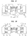
- FIG. 27 is a block diagram of an example of the data communication device according to the invention.
- the data communication device of the embodiment is directed to a case where transmission and reception circuits are integrated in an IC.
- An arithmetic processor 2711 , the transmission-side device 110 , and the reception-side device 120 are integrated as a single arithmetic processing IC 2710 .
- a storage device 2721 , the transmission-side device 110 , and the reception-side device 120 are integrated as a single storage IC 2720 .
- the semiconductor integrated circuit devices 2710 and 2720 are mounted on a mounting board such as a printed board, and the transmission line 101 _m is formed by a printed wire formed on the printed board.
- FIG. 28 is a block diagram showing another embodiment of the data communication device according to the invention. Different from FIG. 27 in which the transmission-side device and the reception-side device are integrated in an IC, transmission-side and reception-side devices in the data communication device of the embodiment are externally provided for an IC. As shown in FIG. 28 , separately from an arithmetic processing IC 2810 , the transmission-side device 110 and the reception-side device 120 are mounted. The arithmetic processing IC 2810 and the transmission-side and reception-side devices are connected by parallel link.
- the transmission-side device 110 and the reception-side device 120 are mounted separately from a storage IC 2820 , and the storage IC 2820 and the transmission-side and reception-side devices are connected by parallel link.
- the distance between the arithmetic processing IC and the storage IC generally, the distance between the arithmetic processing IC 2810 and the transmission-side and reception-side devices or the distance between the storage IC 2820 and the transmission-side and reception-side devices can be made short. Thus, an influence of the timing skew can be suppressed.
- the arithmetic processing IC 2810 and the storage IC 2820 are formed by existing semiconductor chips, combined with semiconductor chips serving as the transmission-side device 110 and the reception-side device 120 to which the invention is applied, and the semiconductor chips are sealed with the same package, thereby obtaining an apparently-single semiconductor integrated circuit device.
- the distance between the arithmetic processing IC 2810 and the transmission/reception-side devices or the distance between the storage IC 2820 and the transmission/reception-side devices can be generally made short. Alternately, they are connected to each other via bonding wires, thereby achieving connection in which the influence of the inductance component of an external terminal is eliminated.
- Clock signals have to be supplied to the transmission-side devices 110 and 110 _ 2 and the high-speed reception-side device 120 _ 2 in the invention.
- the configuration of data encoding shown in FIG. 3 of the transmission-side device and that of the reception-side device have to be the same but do not have to be fixed.
- the invention can be applied to so-called data encryption of concealing the contents of data passing on an external transmission line.
- the arithmetic processing IC designates a specific address to the storage IC, and transmits an instruction of writing operation and data to be written.
- the address signal, a write flag, and write data are encoded and transmitted as described above.
- the address, flag, and data are transferred a plurality of times in serial.
- the arithmetic processing IC performs data communication of designating a specific address in the storage IC.
- a designated memory cell is selected, and stored data is read.
- the storage IC performs the data communication of the stored data to the arithmetic processing IC.
- the embodiment Since the embodiment is characterized by high-speed data communication, it is directed to perform communication of a large amount of data. Therefore, in writing or reading data of about four bits, by performing an operation as described above, an effect which is not so large is produced. Consequently, in the writing operation, in the arithmetic processing IC, a specific address range is designated, and a writing operation instruction and a large amount of data to be written are transmitted. In the storage IC, memory cells in the address range are continuously selected and the received data is written.
- a specific address range is designated by the arithmetic processing IC.
- the memory cells in the designated address range are continuously selected and the stored data is read and continuously transmitted.
- a buffer memory may be provided for the arithmetic processing IC.
- a device address is assigned to each of the peripheral devices including the storage IC. By using the device addresses, data communication between specific ICs is performed.
- a plurality of devices are connected to a transmission line, it is necessary to adjust which one of the devices has the right of using the transmission line. It is sufficient to provide each device with an adjusting circuit regarding usage of the transmission line or to provide a dedicated adjusting circuit on the system.
- the commands (Command0, Command1, and Command2) can be used.
- a circuit for performing encoding so that transition takes place in at least one of levels of transmission data synchronously with a transmission clock and a circuit for generating a transmission circuit in a form of level transition from the encoded transmission data can be variously modified.
- the concrete configuration of a circuit for receiving the signal in the form of level transition generated as described above can be also variously modified.
- the present invention can be widely used for a data communication method and a data communication device for transmitting data consisting of a plurality of bits in parallel.
- transition in a transmission line always takes place in each data, so that it is unnecessary to transmit a clock or a data strobe signal in addition to data. Since the clock or data strobe signal is not used, the timing margin for a skew between a clock and data and a jitter is narrowed. By applying the invention, the timing margin is widened. Thus, higher-speed data transfer can be achieved, in addition to data, a signal having no data and a command can be transmitted, and signal pads and transmission lines of the amount can be reduced.
Abstract
Description
f(D(t)[3:0])=T(t)[5:0] (1)
6 C 3=20 (2)
L(t)[m]=T(t)[m]*L(t−1)[m] (3)
T(t)[m]=L(t)[m]*L(t−1)[m] (4)
ΔV=L(di/dt) (5)
- i) the level of the transmission line 101_m changes,
- ii) decoding is performed by the
decoder 121, - iii) the data
valid flag 128 is set, - iv) the level of the transmission line 101_m is latched by the D-type flip-
flop 123 —_m, - v) decoding is performed by the
decoder 121, and - vi) the data
valid flag 128 is cleared.
4×tCK>tDF+tFF (7)
tCK>tFF+2(tEO+tDF) (8)
3×tCK>tFF+tEO+tDE (9)
5 C 3+5 C 2=20 (10)
Log2(m C u)bits
- (1) By encoding data of N bits (N being 2 or larger) to transmission data of M bits (M being 3 or larger) on a transmission side, generating a transmission signal in which transition takes place in at least one level of any of the transmission data synchronously with a transmission clock and transmitting the transmission signal to a transmission line on the transmission side, recognizing transition in the signal of the M bits received via the transmission line and detecting the reception data of the M bits synchronized with the transmission clock on a reception side, and decoding the M-bit reception data to the original N-bit data on the reception side, effects are produced such that it becomes unnecessary to set a time margin for a jitter in a clock and a skew of data and expansion of the timing margin or increase in data transfer speed can be realized.
- (2) In addition, the transmission data is encoded so that at least one bit out of the M bits has one of binary logic values, the level of the transmission data having the one of the logic values in the M-bit transmission data in the transmission signal is shifted synchronously with the transmission clock, and the transmission data having the other logic value is maintained at the same level, thereby producing an effect such that a transmission signal having level transition in correspondence with the transmission data synchronously with the transmission clock can be generated with a simple configuration.
- (3) In addition, two or larger bits of the same value out of the M bits have the one of logic values. Consequently, an effect such that a jitter which occurs in a transmission signal due to simultaneous switching noise can be lessened is obtained.
- (4) In addition, on the reception side, transition in the reception signal is detected, a timing signal is generated, and the M-bit reception data in the reception signal is detected by the timing signal. Therefore, an effect is produced such that the transmission signal sent in the form of signal transition can be converted to a reception signal of a binary level with a simple configuration.
- (5) In addition, by over-sampling the reception signal synchronously with a timing signal having a frequency which is a plurality of times as high as the transmission clock and receiving a plurality of sets of reception data on the reception side, and detecting one accurate reception data from the reception data on the reception side, an effect such that very-reliable reception data can be obtained without being influenced by a jitter and a skew included in the reception signal is produced.
- (6) In addition, by converting a plurality of pieces of transmission data to parallel data and encoding each of the plurality of pieces of transmission data to transmission data of the M bits on the transmission side, generating the transmission signal as serial data and transmitting the transmission signal synchronously with a transmission clock of a cycle corresponding to time shorter than time required for encoding on the transmission side, recognizing transition in a reception signal of the M bits received via the transmission line and detecting the reception data of the M bits synchronized with the transmission clock on the reception side, converting the detected serial data into a plurality of pieces of parallel data and decoding the parallel data to the N-bit data on the reception side, an effect such that higher-speed data communication can be realized is obtained.
- (7) In addition, the transmission signal includes the N-bit data and a control signal used for data communication, and transition takes place in signals of the same number which is two or larger in the N-bit data including the control signal. Therefore, an effect such that data communication can be performed easily at high speed while substantially reducing the number of signals is obtained.
- (8) In addition, the control signal includes a signal indicative of absence of data to be transmitted. Consequently, an effect such that very flexible data communication in which a function of masking transmission data is provided, a dummy cycle is inserted to adjust a timing, or the like can be realized is produced.
- (9) By providing a data communication device including: a transmission-side device including an encoder for encoding data of N bits (N being 2 or larger) to transmission data of M bits (M being 3 or larger), and a transmission circuit for outputting a transmission signal in which transition takes place in at least one level of any of the transmission data synchronously with a transmission clock; a transmission line to which the transmission signal of the transmission circuit is transmitted; and a reception-side device including a reception circuit for recognizing transition in a reception signal of the M bits received via the transmission line and detecting the reception data of the M bits on the basis of the transmission clock and a decoder for decoding the reception data to the N-bit data, effects are produced such that it becomes unnecessary to set a time margin for a jitter in a clock and a skew of data, and the data communication device capable of expanding the timing margin or increasing data transfer speed can be realized.
- (10) In addition, the transmission-side device includes a signal processing circuit for generating the N-bit data, and the reception-side device includes a signal processing circuit for processing the N-bit data. With the configuration, an effect such that a data processing system having a high-speed data communication function can be realized is produced.
- (11) In addition, by forming the transmission-side device on a single semiconductor chip, an effect such that high-speed data communication and miniaturization of the system can be achieved is obtained.
- (12) In addition, by forming the reception-side device on a single semiconductor chip, an effect such that high-speed data communication and miniaturization of the system can be achieved is obtained.
- (13) In addition, the signal processing circuit of the transmission-side device is formed on a first semiconductor ship, the encoder and the transmission circuit are formed on a second semiconductor chip, and the first and second semiconductor chips are integrally sealed to form an apparently single semiconductor integrated circuit device, the signal processing circuit of the reception-side device is formed on a third semiconductor chip, the reception circuit and the decoder are formed on a fourth semiconductor chip, and the third and fourth semiconductor chips are integrally sealed to form an apparently single semiconductor integrated circuit device. With the configuration, an effect such that the system realizing high performance and miniaturization while using the existing semiconductor chips can be realized is obtained.
- (14) In addition, the transmission-side device is constructed by a single semiconductor integrated circuit device, the reception-side device is constructed by a single semiconductor integrated circuit device, and the transmission line is wiring means formed on a mounting board on which the semiconductor integrated circuit devices constructing the transmission-side device and the reception-side device are mounted. With the configuration, an effect such that the system realizing high performance and miniaturization can be realized is obtained.
- (15) In addition, the encoder generates transmission data in which at least one bit out of M bits has one of binary logic values, and the transmission circuit generates a transmission signal which shifts the level of the data having the one of logic values out of the M-bit transmission data synchronously with a transmission clock and which makes the data having the other logic value maintained at the same level. Consequently, an effect such that the transmission signal having level transition in correspondence with transmission data can be generated synchronously with a transmission clock with a simple configuration is produced.
- (16) In addition, the encoder generates transmission data in which bits of the same number which is two or larger out of the M bits have the one of logic values, thereby producing an effect such that a jitter in a transmission signal which is caused by simultaneous switching noise can be lessened.
- (17) In addition, the reception circuit detects the transition in the reception signal, generates a timing signal, and detects reception data of M bits by the timing signal. Consequently, an effect such that a transmission signal transmitted in the form of signal transition can be converted to a binary-level reception signal with a simple configuration is produced.
- (18) In addition, the reception circuit over-samples a reception signal by a timing signal having a frequency a plurality of times as high as that of the transmission clock, receives plural sets of reception data, and detects one accurate reception data from the reception data, thereby producing an effect that very reliable reception data can be obtained without being influenced by a jitter or a skew included in the reception signal.
- (19) In addition, the transmission circuit converts the plurality of pieces of transmission data to parallel transmission data and encodes the parallel transmission data to the M-bit transmission data, the transmission circuit converts the transmission data to serial data, generates the transmission signal, and transmits the transmission signal to a transmission line synchronously with a transmission clock of a cycle corresponding to time shorter than time required for encoding, the reception circuit recognizes transition in a reception signal of the M bits received via the transmission line and detects the M-bit reception data synchronized with the transmission clock, and the decoder converts the detected serial data to a plurality of pieces of parallel data, and decodes the parallel data to the N-bit data. Thus, an effect such that a higher-speed data communication device can be realized is obtained.
- (20) In addition, the encoder generates transmission data of M bits including the N-bit data and a control signal used for data communication, and the transmission circuit generates transmission signals in which transition occurs in signals of the same number which is two or larger including the control signal. With the configuration, an effect such that a high-speed easy-to-operate data communication device can be obtained while substantially reducing the number of signals is obtained.
- (21) In addition, by including a signal indicative of absence of data to be transmitted in the control signal, an effect such that a very flexible data communication device in which a function of masking transmission data, a dummy cycle is inserted to adjust a timing, or the like can be obtained is produced.
- (22) In addition, by using first MOSFETs connected in parallel for receiving a reception signal of M bits and each having an equivalent conductance characteristic and second MOSFETs of M pieces connected in parallel, in which (M−1) MOSFETs have conductance equivalent to that of the first MOSFETs, and one MOSFET has a conductance which is the half of the conductance, supplying a voltage corresponding to one of levels of the reception signal to gates of MOSFETs of the number corresponding to the number of bits having the one of logic values, which include the MOSFET having the half conductance, supplying a voltage corresponding to the other level of the reception signal to the gates of the remaining MOSFETs, and detecting a difference between a current flowing in the first MOSFETs and a current flowing in the second MOSFETs, an effect such that validity/invalidity of the reception signal can be detected at high speed is produced.
Claims (1)
Priority Applications (3)
| Application Number | Priority Date | Filing Date | Title |
|---|---|---|---|
| US10/377,721 US7397879B2 (en) | 2001-11-01 | 2003-03-04 | Data communication method and data communication device and semiconductor device |
| US10/377,720 US7397878B2 (en) | 2001-11-01 | 2003-03-04 | Data communication method and data communication device and semiconductor device |
| US10/377,703 US7359471B2 (en) | 2001-11-01 | 2003-03-04 | Data communication method and data communication device and semiconductor device |
Applications Claiming Priority (2)
| Application Number | Priority Date | Filing Date | Title |
|---|---|---|---|
| JP2001-336373 | 2001-11-01 | ||
| JP2001336373A JP2003143242A (en) | 2001-11-01 | 2001-11-01 | Data communication method and data communication apparatus |
Related Child Applications (3)
| Application Number | Title | Priority Date | Filing Date |
|---|---|---|---|
| US10/377,720 Continuation US7397878B2 (en) | 2001-11-01 | 2003-03-04 | Data communication method and data communication device and semiconductor device |
| US10/377,721 Continuation US7397879B2 (en) | 2001-11-01 | 2003-03-04 | Data communication method and data communication device and semiconductor device |
| US10/377,703 Continuation US7359471B2 (en) | 2001-11-01 | 2003-03-04 | Data communication method and data communication device and semiconductor device |
Publications (2)
| Publication Number | Publication Date |
|---|---|
| US20030081688A1 US20030081688A1 (en) | 2003-05-01 |
| US7319730B2 true US7319730B2 (en) | 2008-01-15 |
Family
ID=19151211
Family Applications (4)
| Application Number | Title | Priority Date | Filing Date |
|---|---|---|---|
| US10/270,693 Expired - Fee Related US7319730B2 (en) | 2001-11-01 | 2002-10-16 | Data communication method and data communication device and semiconductor device |
| US10/377,721 Expired - Fee Related US7397879B2 (en) | 2001-11-01 | 2003-03-04 | Data communication method and data communication device and semiconductor device |
| US10/377,720 Expired - Fee Related US7397878B2 (en) | 2001-11-01 | 2003-03-04 | Data communication method and data communication device and semiconductor device |
| US10/377,703 Expired - Fee Related US7359471B2 (en) | 2001-11-01 | 2003-03-04 | Data communication method and data communication device and semiconductor device |
Family Applications After (3)
| Application Number | Title | Priority Date | Filing Date |
|---|---|---|---|
| US10/377,721 Expired - Fee Related US7397879B2 (en) | 2001-11-01 | 2003-03-04 | Data communication method and data communication device and semiconductor device |
| US10/377,720 Expired - Fee Related US7397878B2 (en) | 2001-11-01 | 2003-03-04 | Data communication method and data communication device and semiconductor device |
| US10/377,703 Expired - Fee Related US7359471B2 (en) | 2001-11-01 | 2003-03-04 | Data communication method and data communication device and semiconductor device |
Country Status (2)
| Country | Link |
|---|---|
| US (4) | US7319730B2 (en) |
| JP (1) | JP2003143242A (en) |
Cited By (4)
| Publication number | Priority date | Publication date | Assignee | Title |
|---|---|---|---|---|
| US7412673B1 (en) * | 2006-01-30 | 2008-08-12 | Xilinx, Inc. | Integrated system noise management—bounce voltage |
| US20100056066A1 (en) * | 2008-09-01 | 2010-03-04 | Hynix Semiconductor, Inc. | Circuit for transmitting and receiving data and control method thereof |
| US11467623B2 (en) * | 2018-10-26 | 2022-10-11 | Magnachip Semiconductor, Ltd. | Reception device |
| US11532362B2 (en) | 2020-09-16 | 2022-12-20 | Kioxia Corporation | Semiconductor memory device and method for driving the same |
Families Citing this family (5)
| Publication number | Priority date | Publication date | Assignee | Title |
|---|---|---|---|---|
| US7295604B2 (en) * | 2003-11-24 | 2007-11-13 | International Business Machines Corporation | Method for determining jitter of a signal in a serial link and high speed serial link |
| US8134194B2 (en) * | 2008-05-22 | 2012-03-13 | Micron Technology, Inc. | Memory cells, memory cell constructions, and memory cell programming methods |
| US9071239B2 (en) | 2013-03-13 | 2015-06-30 | Qualcomm Incorporated | Method and semiconductor apparatus for reducing power when transmitting data between devices in the semiconductor apparatus |
| US9118457B2 (en) * | 2013-03-15 | 2015-08-25 | Qualcomm Incorporated | Multi-wire single-ended push-pull link with data symbol transition based clocking |
| CN114329644B (en) * | 2021-11-17 | 2023-03-24 | 芯华章科技股份有限公司 | Method, device and storage medium for carrying out encryption simulation on logic system design |
Citations (14)
| Publication number | Priority date | Publication date | Assignee | Title |
|---|---|---|---|---|
| US5012467A (en) * | 1989-10-10 | 1991-04-30 | 3Com Corporation | Method and apparatus for collision detection in a local area network transceiver |
| JPH05114924A (en) | 1991-10-23 | 1993-05-07 | Matsushita Electric Ind Co Ltd | Method and device for data transfer |
| US5278902A (en) * | 1992-12-30 | 1994-01-11 | Intel Corporation | Method and apparatus for transition direction coding |
| US5408501A (en) | 1993-04-06 | 1995-04-18 | Conner Peripherals, Inc. | Data transfer system |
| US5491713A (en) * | 1993-04-28 | 1996-02-13 | Hughes Aircraft Company | Minimized oversampling Manchester decoder |
| US5598442A (en) * | 1994-06-17 | 1997-01-28 | International Business Machines Corporation | Self-timed parallel inter-system data communication channel |
| JPH11308281A (en) | 1998-04-22 | 1999-11-05 | Sony Corp | Digital signal transmitter and its method, digital signal transmitter and digital signal receiver |
| US6021011A (en) * | 1993-02-01 | 2000-02-01 | Cirrus Logic, Inc. | Synchronous read channel employing a digital center frequency setting for a variable frequency oscillator in discrete time timing recovery |
| US6222893B1 (en) * | 1998-07-17 | 2001-04-24 | Nec Corporation | Synchronizing circuit |
| US20020008682A1 (en) | 2000-07-18 | 2002-01-24 | Park Jin-Ho | Flat panel display with an enhanced data transmission |
| US6362757B1 (en) | 1999-08-20 | 2002-03-26 | Electronics And Telecommunications Research Institute | Method and apparatus for encoding MB810 line code with the characteristics of minimum bandwidth and DC-free |
| US6463092B1 (en) * | 1998-09-10 | 2002-10-08 | Silicon Image, Inc. | System and method for sending and receiving data signals over a clock signal line |
| US6763477B1 (en) * | 2000-07-31 | 2004-07-13 | Hewlett-Packard Development Company, L.P. | Method and apparatus for transmitting and receiving data using a self clocking link protocol |
| US6959058B2 (en) | 2000-09-02 | 2005-10-25 | Samsung Electronics Co., Ltd. | Data recovery apparatus and method for minimizing errors due to clock skew |
Family Cites Families (5)
| Publication number | Priority date | Publication date | Assignee | Title |
|---|---|---|---|---|
| FR2606239A1 (en) * | 1986-10-30 | 1988-05-06 | Bull Sa | METHOD AND DEVICE FOR TRANSMITTING DIGITAL DATA |
| GB2287622B (en) * | 1994-03-17 | 1998-10-28 | Nissan Motor | Multiplex serial data communication circuit network and method and motor control system and method using multiplex serial data communication circuit network |
| KR0157924B1 (en) * | 1995-12-23 | 1998-12-15 | 문정환 | Data transfer system and its method |
| US6134285A (en) * | 1997-05-28 | 2000-10-17 | Integrated Memory Logic, Inc. | Asynchronous data receiving circuit and method |
| US6460092B1 (en) * | 1999-05-26 | 2002-10-01 | Industrial Technology Research Institute | Integrated circuit for distributed-type input/output control |
-
2001
- 2001-11-01 JP JP2001336373A patent/JP2003143242A/en active Pending
-
2002
- 2002-10-16 US US10/270,693 patent/US7319730B2/en not_active Expired - Fee Related
-
2003
- 2003-03-04 US US10/377,721 patent/US7397879B2/en not_active Expired - Fee Related
- 2003-03-04 US US10/377,720 patent/US7397878B2/en not_active Expired - Fee Related
- 2003-03-04 US US10/377,703 patent/US7359471B2/en not_active Expired - Fee Related
Patent Citations (15)
| Publication number | Priority date | Publication date | Assignee | Title |
|---|---|---|---|---|
| US5012467A (en) * | 1989-10-10 | 1991-04-30 | 3Com Corporation | Method and apparatus for collision detection in a local area network transceiver |
| JPH05114924A (en) | 1991-10-23 | 1993-05-07 | Matsushita Electric Ind Co Ltd | Method and device for data transfer |
| US5278902A (en) * | 1992-12-30 | 1994-01-11 | Intel Corporation | Method and apparatus for transition direction coding |
| US6021011A (en) * | 1993-02-01 | 2000-02-01 | Cirrus Logic, Inc. | Synchronous read channel employing a digital center frequency setting for a variable frequency oscillator in discrete time timing recovery |
| US5408501A (en) | 1993-04-06 | 1995-04-18 | Conner Peripherals, Inc. | Data transfer system |
| JPH08508623A (en) | 1993-04-06 | 1996-09-10 | コナー ペリフェラルズ,インコーポレイティド | Data communication system |
| US5491713A (en) * | 1993-04-28 | 1996-02-13 | Hughes Aircraft Company | Minimized oversampling Manchester decoder |
| US5598442A (en) * | 1994-06-17 | 1997-01-28 | International Business Machines Corporation | Self-timed parallel inter-system data communication channel |
| JPH11308281A (en) | 1998-04-22 | 1999-11-05 | Sony Corp | Digital signal transmitter and its method, digital signal transmitter and digital signal receiver |
| US6222893B1 (en) * | 1998-07-17 | 2001-04-24 | Nec Corporation | Synchronizing circuit |
| US6463092B1 (en) * | 1998-09-10 | 2002-10-08 | Silicon Image, Inc. | System and method for sending and receiving data signals over a clock signal line |
| US6362757B1 (en) | 1999-08-20 | 2002-03-26 | Electronics And Telecommunications Research Institute | Method and apparatus for encoding MB810 line code with the characteristics of minimum bandwidth and DC-free |
| US20020008682A1 (en) | 2000-07-18 | 2002-01-24 | Park Jin-Ho | Flat panel display with an enhanced data transmission |
| US6763477B1 (en) * | 2000-07-31 | 2004-07-13 | Hewlett-Packard Development Company, L.P. | Method and apparatus for transmitting and receiving data using a self clocking link protocol |
| US6959058B2 (en) | 2000-09-02 | 2005-10-25 | Samsung Electronics Co., Ltd. | Data recovery apparatus and method for minimizing errors due to clock skew |
Non-Patent Citations (2)
| Title |
|---|
| JEDEC Standard JESD79, "Double Data Rate (DDR) SDRAM Specification", Jun. 2000, pp. 1-72. |
| Kitayama, Hiroyuki, "IEEE 1394 Architecture (Details on the physical layer, serial bus management, and protocol)", Interface, Jul. 1999, pp. 58-67 (with English translation). |
Cited By (5)
| Publication number | Priority date | Publication date | Assignee | Title |
|---|---|---|---|---|
| US7412673B1 (en) * | 2006-01-30 | 2008-08-12 | Xilinx, Inc. | Integrated system noise management—bounce voltage |
| US20100056066A1 (en) * | 2008-09-01 | 2010-03-04 | Hynix Semiconductor, Inc. | Circuit for transmitting and receiving data and control method thereof |
| US8036050B2 (en) * | 2008-09-01 | 2011-10-11 | Hynix Semiconductor Inc. | Circuit for transmitting and receiving data and control method thereof |
| US11467623B2 (en) * | 2018-10-26 | 2022-10-11 | Magnachip Semiconductor, Ltd. | Reception device |
| US11532362B2 (en) | 2020-09-16 | 2022-12-20 | Kioxia Corporation | Semiconductor memory device and method for driving the same |
Also Published As
| Publication number | Publication date |
|---|---|
| US7397878B2 (en) | 2008-07-08 |
| US20030189985A1 (en) | 2003-10-09 |
| US20030161409A1 (en) | 2003-08-28 |
| US7397879B2 (en) | 2008-07-08 |
| US20030156653A1 (en) | 2003-08-21 |
| US7359471B2 (en) | 2008-04-15 |
| US20030081688A1 (en) | 2003-05-01 |
| JP2003143242A (en) | 2003-05-16 |
Similar Documents
| Publication | Publication Date | Title |
|---|---|---|
| US5777567A (en) | System and method for serial to parallel data conversion using delay line | |
| US5798720A (en) | Parallel to serial data converter | |
| KR101173942B1 (en) | Data transmission device, data receiving device, data transmitting system and method for transmitting data | |
| US7307554B2 (en) | Parallel data transmission method and parallel data transmission system | |
| KR100885869B1 (en) | Method and Record readable medium, and apparatus for reducing noise by using Preamble Code in single ended parallel interface | |
| US7755405B2 (en) | DLL circuit and method of controlling the same | |
| US8199035B2 (en) | Method, device, and system for data communication with preamble for reduced switching noise | |
| US7319730B2 (en) | Data communication method and data communication device and semiconductor device | |
| CN116153362B (en) | Delay feedback method and delay feedback storage structure for read latency counter | |
| US5748123A (en) | Decoding apparatus for Manchester code | |
| US6583654B2 (en) | Clock synchronization device | |
| TWI400915B (en) | Method and apparatus for generating a serial clock without a pll | |
| CN110545093A (en) | semiconductor device and semiconductor test equipment | |
| KR100260795B1 (en) | An interface system for on-chip or off-chip interconnection | |
| JPH1168861A (en) | Simultaneous two-way transmission reception method and simultaneous two-way transmission reception circuit | |
| KR20000013044A (en) | Encoder for interfacing of high speed and serial bus | |
| JP4377420B2 (en) | Simultaneous bidirectional data transmission / reception system | |
| KR0157923B1 (en) | Menchester decoder | |
| JP3976923B2 (en) | Semiconductor device | |
| KR100314675B1 (en) | Apparatus for bi-phase in digital television | |
| JPH05191296A (en) | 1-7rll code conversion circuit | |
| JP2001053734A (en) | Optical reception circuit for burst optical signal | |
| JP2005101886A (en) | Pulse regeneration circuit |
Legal Events
| Date | Code | Title | Description |
|---|---|---|---|
| AS | Assignment |
Owner name: HITACHI, LTD., JAPAN Free format text: ASSIGNMENT OF ASSIGNORS INTEREST;ASSIGNORS:OKUDA, YUICHI;SAKATA, TAKESHI;SATO, TAKASHI;REEL/FRAME:013391/0291;SIGNING DATES FROM 20020927 TO 20020930 |
|
| AS | Assignment |
Owner name: RENESAS TECHNOLOGY CORPORATION, JAPAN Free format text: ASSIGNMENT OF ASSIGNORS INTEREST;ASSIGNOR:HITACHI, LTD.;REEL/FRAME:014244/0278 Effective date: 20030912 |
|
| STCF | Information on status: patent grant |
Free format text: PATENTED CASE |
|
| FEPP | Fee payment procedure |
Free format text: PAYOR NUMBER ASSIGNED (ORIGINAL EVENT CODE: ASPN); ENTITY STATUS OF PATENT OWNER: LARGE ENTITY Free format text: PAYER NUMBER DE-ASSIGNED (ORIGINAL EVENT CODE: RMPN); ENTITY STATUS OF PATENT OWNER: LARGE ENTITY |
|
| AS | Assignment |
Owner name: NEC ELECTRONICS CORPORATION, JAPAN Free format text: MERGER;ASSIGNOR:RENESAS TECHNOLOGY CORP.;REEL/FRAME:024879/0190 Effective date: 20100401 Owner name: RENESAS ELECTRONICS CORPORATION, JAPAN Free format text: CHANGE OF NAME;ASSIGNOR:NEC ELECTRONICS CORPORATION;REEL/FRAME:024864/0635 Effective date: 20100401 |
|
| FPAY | Fee payment |
Year of fee payment: 4 |
|
| FPAY | Fee payment |
Year of fee payment: 8 |
|
| AS | Assignment |
Owner name: RENESAS ELECTRONICS CORPORATION, JAPAN Free format text: CHANGE OF ADDRESS;ASSIGNOR:RENESAS ELECTRONICS CORPORATION;REEL/FRAME:044928/0001 Effective date: 20150806 |
|
| FEPP | Fee payment procedure |
Free format text: MAINTENANCE FEE REMINDER MAILED (ORIGINAL EVENT CODE: REM.); ENTITY STATUS OF PATENT OWNER: LARGE ENTITY |
|
| LAPS | Lapse for failure to pay maintenance fees |
Free format text: PATENT EXPIRED FOR FAILURE TO PAY MAINTENANCE FEES (ORIGINAL EVENT CODE: EXP.); ENTITY STATUS OF PATENT OWNER: LARGE ENTITY |
|
| STCH | Information on status: patent discontinuation |
Free format text: PATENT EXPIRED DUE TO NONPAYMENT OF MAINTENANCE FEES UNDER 37 CFR 1.362 |
|
| FP | Lapsed due to failure to pay maintenance fee |
Effective date: 20200115 |