US6151179A - Signal processing circuit with feedback extracted from a sampled analog error signal - Google Patents
Signal processing circuit with feedback extracted from a sampled analog error signal Download PDFInfo
- Publication number
- US6151179A US6151179A US08/891,517 US89151797A US6151179A US 6151179 A US6151179 A US 6151179A US 89151797 A US89151797 A US 89151797A US 6151179 A US6151179 A US 6151179A
- Authority
- US
- United States
- Prior art keywords
- signal
- signal processing
- circuit
- analog
- variable
- Prior art date
- Legal status (The legal status is an assumption and is not a legal conclusion. Google has not performed a legal analysis and makes no representation as to the accuracy of the status listed.)
- Expired - Lifetime
Links
Images

Classifications
-
- G—PHYSICS
- G11—INFORMATION STORAGE
- G11B—INFORMATION STORAGE BASED ON RELATIVE MOVEMENT BETWEEN RECORD CARRIER AND TRANSDUCER
- G11B20/00—Signal processing not specific to the method of recording or reproducing; Circuits therefor
- G11B20/10—Digital recording or reproducing
- G11B20/10009—Improvement or modification of read or write signals
- G11B20/10046—Improvement or modification of read or write signals filtering or equalising, e.g. setting the tap weights of an FIR filter
- G11B20/10055—Improvement or modification of read or write signals filtering or equalising, e.g. setting the tap weights of an FIR filter using partial response filtering when writing the signal to the medium or reading it therefrom
-
- G—PHYSICS
- G11—INFORMATION STORAGE
- G11B—INFORMATION STORAGE BASED ON RELATIVE MOVEMENT BETWEEN RECORD CARRIER AND TRANSDUCER
- G11B20/00—Signal processing not specific to the method of recording or reproducing; Circuits therefor
- G11B20/10—Digital recording or reproducing
- G11B20/10009—Improvement or modification of read or write signals
-
- G—PHYSICS
- G11—INFORMATION STORAGE
- G11B—INFORMATION STORAGE BASED ON RELATIVE MOVEMENT BETWEEN RECORD CARRIER AND TRANSDUCER
- G11B5/00—Recording by magnetisation or demagnetisation of a record carrier; Reproducing by magnetic means; Record carriers therefor
- G11B5/02—Recording, reproducing, or erasing methods; Read, write or erase circuits therefor
- G11B5/09—Digital recording
Definitions
- the present invention relates to analog signal processing, and more particularly to an improved signal processing apparatus having reduced processing power requirements.
- Analog signal processing circuits such as those used to process analog signals read by disk drive transducer heads from magnetic disks typically use feedback or decision aided gain and timing control to control tracking of the recorded data.
- Known Partial Response Maximum Likelihood Type IV channels employ a variable gain amplifier in the channel for amplification of the analog disk signal and a variable clock oscillator for controlling the synchronization of the analog disk signal sampling.
- a gain error signal is developed from the analog disk signal to control the amplifier gain
- a timing error signal is developed from the analog disk signal to control the oscillator frequency.
- Known signal processing systems for disk drive channel tracking control have a gain error circuit for developing the gain error signal from the analog disk signal and a discrete timing error circuit for developing the timing error signal from the analog disk signal.
- Known signal processing circuits also typically may include detection circuitry separate from the error circuits for developing an idealized digital target value signal from the amplified and equalized signal provided in the data channel. Typical timing and gain error circuits directly process the analog disk signal.
- the known signal processing systems are subject to problems. Because the analog disk signal is relatively large, the power requirement for processing the signal is undesireably large. Also the use of two separate error circuits for developing gain and timing error signals results in excessive power use and in undesirable circuit complexity.
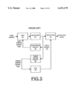
- FIG. 3 is a block diagram of a typical prior art Type IV Partial Response Maximum Likelihood (PRML-IV) read data channel;
- PRML-IV Type IV Partial Response Maximum Likelihood
- FIG. 4 is a block diagram of a read data channel signal processing system embodying the present invention.
- FIG. 6 is a schematic diagram of the gain and timing error circuit of the system of FIG. 4;
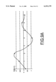
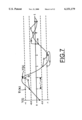
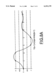
- FIG. 7 is a graph showing an analog ac class IV partial response signal sampled at regular time intervals, together with the corresponding ideal target value for each sample instance;
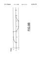
- FIGS. 8A, 8B and 8C show three differential waveforms that are generated and held by the signal error generating circuit of FIG. 5;
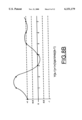
- FIGS. 9A and 9B respectively show an input ac waveform and the class IV partial response target values determined from the input waveform by the signal error generating circuit of FIG. 5;
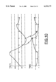
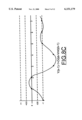
- FIG. 10 shows the output error signal waveform provided by the signal error generating circuit of FIG. 5 from the input waveform
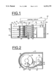
- FIG. 1 is a simplified, partly schematic illustration of a data storage disk file 10 including a data storage medium generally designated as 12 and an interface control unit generally designated as 14.
- the data storage medium 12 is a rigid magnetic disk drive unit 12, although other media could be used.
- the disk drive unit 12 is illustrated in simplified form sufficient for an understanding of the present invention, in view of the fact that the present invention has utility with a wide variety of drive units.
- the disk drive unit 12 includes a stack 16 of disks 18 each having at least one magnetic disk surface 20.
- the disks 18 are mounted parallel to one another for simultaneous rotation on and by an integrated spindle and motor assembly 26.
- Data is written to or read from each disk surface 20 of each disk 18 by a corresponding transducer or read/write head 28 movable across the rotating disk surface 20.
- a head 28 is provided for each surface 20.
- each disk 18 is shown with a single data surface 20 and a single corresponding head 28. In practice, each disk 18 may have two opposed data surfaces 20, each with a corresponding head 28.
- Transducer heads 28 are mounted on flexure springs 30 carried by arms 32 ganged together for simultaneous pivotal movement about a common axis provided by a support spindle 34.
- One of the arms 34 includes an extension 36 driven in a pivotal motion by a head drive motor 38.
- the motor 38 is illustrated as a voice coil type motor with a coil 39 cooperating with a magnet and core assembly (not seen) controlled for moving the transducer heads 28 in synchronism along radial paths over the magnetic disk surfaces 20.
- the coil 39 moves through a fixed magnetic field, the direction and velocity of its movement is controlled by current supplied to the coil 39.
- the components of the disk file 10 are controlled in operation by signals supplied by the control unit 14, including spindle motor control signals on line 26A and head position control signals on line 38A.
- data is written to or recorded upon the disk surfaces 20.
- the recorded data may include synchronization information provided on one or more disk surfaces that may be read by one or more heads 28.
- the synchronization data is read and used to lock the heads 28 in accurate synchronization with the data recorded on the surfaces 20.
- customer data can be written onto or read from the surfaces 20 in regions other than those containing synchronization data.
- customer data can be written onto or read from the surfaces 20 in regions other than those containing synchronization data.
- the system is operated in a tracking mode following the acquisition mode.
- the present invention provides important advantages in the processing of data received from a transducer head 28 operating in the tracking mode.
- the reading of data by the heads 28 from the magnetic disk surfaces 20 is one example of a data communication system where it is necessary to process an analog signal in order to accurately determine the signal information content.
- PRML Partial Response Maximum Likelihood data processing
- FIG. 3 is block diagram of a typical Type IV PRML data read channel.
- the disk signal read from a disk surface 20 by a head 28 is supplied to a variable gain amplifier (VGA) 40.
- VGA variable gain amplifier
- the amplified signal is processed by a filter or equalizer 42 and the equalized signal Y(t) is provided to a detector 44 and detected by one of many methods such as, for example, maximum likelihood detection using the Viterbi algorithm.
- the PR-IV signal Y(t) has three target values of +1, -1 and zero.
- the timing of the detector 44 is maintained by a variable clock oscillator (VCO) 46 in synchronization with the timing of signal variations within the equalized signal Y(t) and the gain of the VGA 40 is controlled to regulate the magnitude of the equalized signal.
- VCO variable clock oscillator
- the gain of the VGA 40 is controlled by a gain error signal Ge(t) provided by a gain error circuit 48 and the timing of the VCO 46 is controlled by a timing error signal Te(t) provided by a timing error circuit 50.
- the error circuits 48 and 50 derive the error signals from the signal Y(t) to provide feedback or decision aided gain and timing control.
- the known processing system of FIG. 3 has disadvantages. In tracking mode the signal Y(t) is relatively large in comparison with the amount by which it differs from the three target values. Because the timing and gain error signals are processed independently of one another, and because the relatively large signal Y(t) is processed directly, the known system requires an undesireably large amount of signal processing power.
- FIG. 4 is an illustration of a signal processing system embodying the present invention.
- the system may be incorporated into the control unit 14 of the data storage disk file 10.
- the disk signal read by a head 28 from a magnetic disk surface 20 is provided to the VGA 40 and equalizer 42 to provide the equalized signal Y(t).
- This sampling or signal Y(t) is provided to a signal error generating circuit 50 also seen in detail in FIG. 5.
- the circuit 50 receives clock timing signals from the VCO 46 and processes the input signal Y(t) to provide both an error signal Ye(k) and an idealized PRML-IV detected output signal Y(k) having a two bit digital value of 0, +1 or -1 at time k.
- the gain and timing error circuit 52 provides the gain error signal Ge(t) for feedback control of the VGA 40 and the timing error signal Te(t) for feedback control of the VCO 46.
- the feedback paths for the signals Ge(t) and Te(t) are seen in FIG. 4 extending from the circuit 52 respectively to the circuits 40 and 46.
- the signal error generating circuit 50 of FIGS. 4 and 5 processes the analog signal Y(t) using a minimum amount of power by reducing the processed signal amplitude without reducing the electronic signal to noise ratio.
- the signal is "folded" around the specific target values of +1, -1 and 0.
- FIG. 7 illustrates the waveform of the analog signal Y(t) with magnitude of the signal along the vertical axis and time along the horizontal axis.
- the analog signal is sampled at regular periods spaced by time "T".
- the sample instances are designated as 0, 1, 2, . . . 7 on the time axis.
- the circuit 50 Rather than processing the relatively large sampled values Y(k), the circuit 50 instead processes relatively smaller error values designated as Ye(k).
- the error values are the amounts by which the sampled values Y(k) differ from the target values Y(k).
- the target values Y(k) are shown by the points marked "x" and designated as 56 in FIG. 7. Each of these points in the PR-IV signal has a target value of +1, -1 or 0.
- the target value for each sampled value Y(k) is determined as shown in the following table 1:
- the error signal is the difference between the target value Y(k) and the sampled value Y(k).
- Ye(k) is equal to Y(k) minus Y(k).
- the value of Ye(k) can alternatively be expressed as in table 2:
- the following table 3 provides a specific numerical example of the target values Y(k), the sampled values Y(k) and the error values Ye(k) as seen in the graph of FIG. 7:
- Processing the relatively smaller error signal Ye(k) rather than the relatively larger sampled signal Y(k) reduces the amount of power needed to process the signal by a factor of three.
- the signal error generating circuit 50 of FIGS. 4 and 5 generates the error signal Ye(k) and the target value signal Y(k) from the input signal Y(k). In general, the circuit 50 generates and stores all three possible target values of +1, -1 and 0 until the one correct target value is known. Once the correct target value is known, a multiplexer switch is used to designate the single correct value of the error signal Ye(k).
- the input signal is designated as Y(k-1) where the expression k-1 means one time period T earlier than time k.
- FIGS. 8A, 8B and 8C show the three differential waveforms produced by the four voltage nodes designated in FIG. 5 as Vpt, Vpb, Vmt and Vmb at time (k-1).
- the waveform is obtained at nodes Vpb and Vmb and provides the error signal Ye(k-1) when the target value Y(k-1) is 0.
- the waveform is obtained at nodes Vpt and Vmb and provides the error signal Ye(k-1) when the target value Y(k) is -1.
- FIG. 8C the waveform is obtained at nodes Vpb and Vmt and provides the error signal Ye(k-1) when the target value Y(k) is +1.
- All four voltage nodes are sampled and held in a pair of sample and hold multiplexer circuits 66 and 68 designated as circuits A and B.
- the four node outputs are thus preserved to retain the information needed to generate the error signal Ye(k-1) at the later time when the target value is known.
- the target value Y(k) is determined from four nodes in the voltage dividers 62 and 64 designated Vcpb, Vcmt, Vcmb and Vcpt.
- the voltages at these nodes are supplied to a detector circuit 69 including a pair of comparators 70 and 72.
- Comparator 70 is a +1 comparator that gives an output value of +1 if Y(k-1) is greater than +0.5. In this case Y(k) is +1.
- Comparator 72 is a -1 comparator that gives an output value of -1 if Y(k-1) is less than -0.5. In this case Y(k) is -1. If Y(k-1) is between -0.5 and +0.5, then the outputs of both comparators 70 and 72 are 0 and Y(k) is 0.
- FIGS. 9A and 9B show the waveform Y(k) (FIG. 9B) that is derived by the circuit of FIG. 5 from the input waveform Y(k-1) (FIG. 9A).
- Each value of Y(k) is determined by the comparators 70 and 72 from the value of the input signal at the sequentially next earlier time k-1.
- the target voltage signal Y(k) has three possible values and can be represented as a two bit digital signal. As seen in FIG. 4, this signal may be outputted for further use or processing, and is also passed to the gain and timing error circuit 52.
- the voltages at the four nodes Vpt, Vmt, Vpb and Vmb are alternately sampled and held by the circuits 66 and 68.
- one circuit 66 or 68 is switched to the sampling mode while the other is in the hold mode.
- each sample and hold circuit is switched to the alternate mode.
- sample and hold A 66 is holding
- sample and hold B 68 is sampling and conversely when sample and hold A 66 is sampling, sample and hold B 68 is holding.
- the signal error generating circuit 50 of FIG. 5 includes an array 74 of switches for selectively interconnecting sampled and held voltages from the sample and hold circuits 66 and 68 to a pair of output nodes 76 and 78.
- the switches 74 are operated in order to pass the error signal Ye(k) to the output nodes 76 and 78.
- Switch SMT-A passes the voltage held in circuit 66 from node Vmt and switch SMT-B passes the voltage held in circuit 68 from node Vmt.
- Switch SPT-A passes the voltage held in circuit 66 from node Vpt and switch SPT-B passes the voltage held in circuit 68 from node Vpt.
- Switch SPB-A passes the voltage held in circuit 66 from node Vpb and switch SPB-B passes the voltage held in circuit 68 from node Vpb.
- Switch SMB-A passes the voltage held in circuit 66 from node Vmb and switch SMB-B passes the voltage held in circuit 68 from node Vmb
- Circuit 79 is preferably a latched zone decode and relay select logic circuit that both controls the operation of the switch array 74 and also outputs the digital target value circuit Y(k) with a two clock pulse delay as described below in connection with FIG. 6.
- the pair of switches to be closed at each clock pulse is selected by circuit 79 from the sample and hold circuit 66 or 68 that is in the holding mode at that time. The pair of switches is selected based upon the value of Y(k) at that time.
- the following table 4 shows the manner in which a pair of switches is selected and closed at each clock pulse:
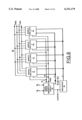
- the gain and timing error circuit 52 seen in FIGS. 4 and 6 receives the error signal Ye(k) and the target value signal Y(k) from the signal error generating circuit 50 and provides timing and gain feedback error signals Ge(t) and Te(t) for the VGA 40 and the VCO 46. Power requirements are reduced by processing the two error signals together, sharing information using analog sampling techniques.
- the preferred embodiment uses the two algorithms set forth below to generate timing and gain error signals in the tracking mode for PRML error detection, but the invention may be employed with other algorithms and in signal processing applications other than PRML.
- a four step sequencer 90 is synchronized by clock pulses from the VC0 46 and sequences the sampling of the four sample and hold circuits 82-88.
- the sequencer 90 is clock synchronized and controls the selection of the particular held, previously sampled values to be used to develop the output error signals Ge(t) and Te(t).
- the timing and error signals Te(t) and Ge(t) are integrated.
- Te(t) integrated would be positive and the VCO 46 is slowed.
- Ge(t) integrated indicates that the gain of the VGA 40 is too low and the gain will increase.
- each sample and hold circuit 82-88 must match in dc offset within a given amplitude.
- the relatively smaller error signal Ye(t) rather than the larger Y(t) signal, gain mismatches are not as critical because large errors in timing and gain are non-linear but when timing and gain errors are close to the PR-IV target values of +1, -1 and 0, then only the offset is critical. This is because Ye(k) is nominally zero when the sampled values are at +1, -1 or 0.
- Interleaving is allowed in class IV partial response maximum likelihood signal channels.
- odd time k signals and even time k signals are processed independently.
- the preferred embodiment disclosed here can be used with interleaved processing by using separate circuits for the two independent processing channels.
Abstract
Description
              TABLE 1
______________________________________
         Y(k) = +1 if Y(k) ≧ 0.5
  Y(k) = 0 if -0.5 < Y(k) < 0.5
  Y(k) = -1 if Y(k) ≦ -0.5
______________________________________
              TABLE 2
______________________________________
         Ye(k) = Y(k) + 1 if Y(k) = -1
  Ye(k) = Y(k) if Y(k) = 0
  Ye(k) = Y(k) - 1 if Y(k) = +1
______________________________________
              TABLE 3
______________________________________
k     0      1      2    3     4    5     6    7
______________________________________
Y (k) 0      +1     -1   -1    -1   0     0    0
  Y (k) -0.2 +0.7 +1.2 -0.7 -1.05 -0.25 +0.2 -0.15
  Ye (k) -0.2 -0.3 +0.2 +0.3 -0.05 -0.25 +0.2 -0.15
______________________________________
              TABLE 4
______________________________________
Y(k)     Hold            Selected Switches
______________________________________
+1       A               SPB-A and SMT-A
  +1 B SPB-B AND SMT-B
  0 A SPB-A AND SMB-A
  0 B SPB-B AND SMB-A
  -1 A SPT-A AND SMB-A
  -1 B SPT-B AND SMB-B
______________________________________
Ge(t)=Y(k-2)*Ye(k-2)
Te(t)=Y(k-2)[Ye(k-1)-Ye(k-3)]
                                  TABLE 5
__________________________________________________________________________
k    1    2    3    4    5    6    7
__________________________________________________________________________
Ye (k)
     -0.32
          -0.47
               +0.2 +0.4 -0.3 -0.45
                                   +0.2
  S/H 0 Sampling Ye (k - 1) Ye (k - 2) Ye (k - 3) Sampling Ye (k - 1) Ye
                                   (k - 2)
    -0.32 -0.32 -0.32  -0.30 -0.30
  S/H 1  Sampling Ye (k - 1) Ye (k - 2) Ye (k - 3) Sampling Ye (k - 1)
                                       -0.47 -0.47 -0.47  -0.45
  S/H 2   Sampling Ye (k - 1) Ye (k - 2) Ye (k - 3) Sampling
      +0.2 +0.2 +0.2
  S/H 3    Sampling Ye (k - 1) Ye (k - 2) Ye (k - 3)
       +0.4 +0.4 +0.4
  Y (k) 0 +1 +1 -1 -1 0 0
  Y (k - 2)   0 +1 +1 -1 -1
  Ge (t)   0 -0.47 +0.2 -0.4 +0.3
  Te (t)    +0.52 +.87 +0.5 +0.85
__________________________________________________________________________
Claims (12)
Priority Applications (1)
| Application Number | Priority Date | Filing Date | Title |
|---|---|---|---|
| US08/891,517 US6151179A (en) | 1997-07-11 | 1997-07-11 | Signal processing circuit with feedback extracted from a sampled analog error signal |
Applications Claiming Priority (1)
| Application Number | Priority Date | Filing Date | Title |
|---|---|---|---|
| US08/891,517 US6151179A (en) | 1997-07-11 | 1997-07-11 | Signal processing circuit with feedback extracted from a sampled analog error signal |
Publications (1)
| Publication Number | Publication Date |
|---|---|
| US6151179A true US6151179A (en) | 2000-11-21 |
Family
ID=25398335
Family Applications (1)
| Application Number | Title | Priority Date | Filing Date |
|---|---|---|---|
| US08/891,517 Expired - Lifetime US6151179A (en) | 1997-07-11 | 1997-07-11 | Signal processing circuit with feedback extracted from a sampled analog error signal |
Country Status (1)
| Country | Link |
|---|---|
| US (1) | US6151179A (en) |
Cited By (7)
| Publication number | Priority date | Publication date | Assignee | Title |
|---|---|---|---|---|
| US20030021429A1 (en) * | 2001-07-30 | 2003-01-30 | Ratcliff David D. | On-the-fly configurable audio processing machine |
| US20060256896A1 (en) * | 2005-05-10 | 2006-11-16 | Seagate Technology Llc | Robust maximum-likelihood based timing recovery |
| US20070047127A1 (en) * | 2005-08-30 | 2007-03-01 | Hutchins Robert A | Dynamically adapting a read channel equalizer |
| US8161361B1 (en) | 2003-01-28 | 2012-04-17 | Marvell International Ltd. | Averaging signals to improve signal interpretation |
| US20150235452A1 (en) * | 2013-03-15 | 2015-08-20 | Magic Leap, Inc. | Blanking techniques in augmented or virtual reality systems |
| US10068374B2 (en) | 2013-03-11 | 2018-09-04 | Magic Leap, Inc. | Systems and methods for a plurality of users to interact with an augmented or virtual reality systems |
| US11170565B2 (en) | 2018-08-31 | 2021-11-09 | Magic Leap, Inc. | Spatially-resolved dynamic dimming for augmented reality device |
Citations (3)
| Publication number | Priority date | Publication date | Assignee | Title |
|---|---|---|---|---|
| US5459757A (en) * | 1994-09-21 | 1995-10-17 | Seagate Technology, Inc. | Timing and gain control circuit for a PRML read channel |
| US5796358A (en) * | 1996-08-01 | 1998-08-18 | Nec Electronics, Inc. | Methods and structure for combined analog and digital automatic gain control in sampled-data receivers |
| US5841602A (en) * | 1994-03-18 | 1998-11-24 | Fujitsu Limited | PRML regenerating apparatus |
-
1997
- 1997-07-11 US US08/891,517 patent/US6151179A/en not_active Expired - Lifetime
Patent Citations (3)
| Publication number | Priority date | Publication date | Assignee | Title |
|---|---|---|---|---|
| US5841602A (en) * | 1994-03-18 | 1998-11-24 | Fujitsu Limited | PRML regenerating apparatus |
| US5459757A (en) * | 1994-09-21 | 1995-10-17 | Seagate Technology, Inc. | Timing and gain control circuit for a PRML read channel |
| US5796358A (en) * | 1996-08-01 | 1998-08-18 | Nec Electronics, Inc. | Methods and structure for combined analog and digital automatic gain control in sampled-data receivers |
Cited By (28)
| Publication number | Priority date | Publication date | Assignee | Title |
|---|---|---|---|---|
| US20030021429A1 (en) * | 2001-07-30 | 2003-01-30 | Ratcliff David D. | On-the-fly configurable audio processing machine |
| US8161361B1 (en) | 2003-01-28 | 2012-04-17 | Marvell International Ltd. | Averaging signals to improve signal interpretation |
| US8359527B1 (en) | 2003-01-28 | 2013-01-22 | Marvell International Ltd. | Averaging signals to improve signal interpretation |
| US8589774B1 (en) | 2003-01-28 | 2013-11-19 | Marvell International Ltd. | Averaging signals to improve signal interpretation |
| US20060256896A1 (en) * | 2005-05-10 | 2006-11-16 | Seagate Technology Llc | Robust maximum-likelihood based timing recovery |
| US7564931B2 (en) * | 2005-05-10 | 2009-07-21 | Seagate Technology Llc | Robust maximum-likelihood based timing recovery |
| US20070047127A1 (en) * | 2005-08-30 | 2007-03-01 | Hutchins Robert A | Dynamically adapting a read channel equalizer |
| US7589927B2 (en) * | 2005-08-30 | 2009-09-15 | International Business Machines Corporation | Dynamically adapting a read channel equalizer |
| US10234939B2 (en) | 2013-03-11 | 2019-03-19 | Magic Leap, Inc. | Systems and methods for a plurality of users to interact with each other in augmented or virtual reality systems |
| US11087555B2 (en) | 2013-03-11 | 2021-08-10 | Magic Leap, Inc. | Recognizing objects in a passable world model in augmented or virtual reality systems |
| US10068374B2 (en) | 2013-03-11 | 2018-09-04 | Magic Leap, Inc. | Systems and methods for a plurality of users to interact with an augmented or virtual reality systems |
| US10126812B2 (en) | 2013-03-11 | 2018-11-13 | Magic Leap, Inc. | Interacting with a network to transmit virtual image data in augmented or virtual reality systems |
| US11663789B2 (en) | 2013-03-11 | 2023-05-30 | Magic Leap, Inc. | Recognizing objects in a passable world model in augmented or virtual reality systems |
| US10163265B2 (en) | 2013-03-11 | 2018-12-25 | Magic Leap, Inc. | Selective light transmission for augmented or virtual reality |
| US10629003B2 (en) | 2013-03-11 | 2020-04-21 | Magic Leap, Inc. | System and method for augmented and virtual reality |
| US10282907B2 (en) | 2013-03-11 | 2019-05-07 | Magic Leap, Inc | Interacting with a network to transmit virtual image data in augmented or virtual reality systems |
| US10304246B2 (en) * | 2013-03-15 | 2019-05-28 | Magic Leap, Inc. | Blanking techniques in augmented or virtual reality systems |
| US10453258B2 (en) | 2013-03-15 | 2019-10-22 | Magic Leap, Inc. | Adjusting pixels to compensate for spacing in augmented or virtual reality systems |
| US10510188B2 (en) | 2013-03-15 | 2019-12-17 | Magic Leap, Inc. | Over-rendering techniques in augmented or virtual reality systems |
| US10553028B2 (en) | 2013-03-15 | 2020-02-04 | Magic Leap, Inc. | Presenting virtual objects based on head movements in augmented or virtual reality systems |
| US20150235452A1 (en) * | 2013-03-15 | 2015-08-20 | Magic Leap, Inc. | Blanking techniques in augmented or virtual reality systems |
| US20150235453A1 (en) * | 2013-03-15 | 2015-08-20 | Magic Leap, Inc. | Rendering based on predicted head movement in augmented or virtual reality systems |
| US11205303B2 (en) | 2013-03-15 | 2021-12-21 | Magic Leap, Inc. | Frame-by-frame rendering for augmented or virtual reality systems |
| US10134186B2 (en) | 2013-03-15 | 2018-11-20 | Magic Leap, Inc. | Predicting head movement for rendering virtual objects in augmented or virtual reality systems |
| US11854150B2 (en) | 2013-03-15 | 2023-12-26 | Magic Leap, Inc. | Frame-by-frame rendering for augmented or virtual reality systems |
| US11170565B2 (en) | 2018-08-31 | 2021-11-09 | Magic Leap, Inc. | Spatially-resolved dynamic dimming for augmented reality device |
| US11461961B2 (en) | 2018-08-31 | 2022-10-04 | Magic Leap, Inc. | Spatially-resolved dynamic dimming for augmented reality device |
| US11676333B2 (en) | 2018-08-31 | 2023-06-13 | Magic Leap, Inc. | Spatially-resolved dynamic dimming for augmented reality device |
Similar Documents
| Publication | Publication Date | Title |
|---|---|---|
| US5438460A (en) | Asynchronous gain adjustment for PRML disk drive systems | |
| US5852524A (en) | Sampled amplitude read channel for processing multiple data streams in a disc storage system | |
| US6337778B1 (en) | Disk drive employing vector addition of primary phase write clock signals for generating secondary phase write clock signal | |
| US5359631A (en) | Timing recovery circuit for synchronous waveform sampling | |
| US5576906A (en) | Synchronous detection of concurrent servo bursts for fine head position in disk drive | |
| US5459757A (en) | Timing and gain control circuit for a PRML read channel | |
| US5258940A (en) | Distributed arithmetic digital filter in a partial-response maximum-likelihood disk drive system | |
| EP0514991A2 (en) | Method and apparatus for digital filter control in a partial-response maximum-likelihood disk drive system | |
| US6614841B1 (en) | Signal processing apparatus | |
| US5903857A (en) | Method and apparatus for calibrating an analog filter in a sampled amplitude read channel | |
| US5768320A (en) | Read system for implementing PR4 and higher order PRML signals | |
| US6151179A (en) | Signal processing circuit with feedback extracted from a sampled analog error signal | |
| JP3648308B2 (en) | Equalizer and magnetic recording signal reproducing apparatus | |
| US5416806A (en) | Timing loop method and apparatus for PRML data detection | |
| KR100445391B1 (en) | Time-domain filters for communication channels | |
| US6005729A (en) | Analog signal processing circuit with integrated gain and timing error signal processing | |
| US6005730A (en) | Signal error generating circuit for an analog signal processing channel | |
| US6078444A (en) | Read channel auxiliary high precision data conversion | |
| US6381292B1 (en) | Phase synchronizing apparatus, phase synchronizing method and disc drive | |
| JP4480584B2 (en) | Adaptive equalization circuit and adaptive equalization method | |
| JPH11232782A (en) | Recording and reproducing device | |
| US5872665A (en) | Programmable write equalization for magnetic data recording | |
| JP2005243222A (en) | Method and device for performing versatile writing pre-compensation | |
| US6163420A (en) | Interleaved analog tracking timing and gain feedback loops for partial response maximum likelihood (PRML) data detection for direct access storage device (DASD) | |
| JP3591902B2 (en) | Demodulation circuit of magnetic recording / reproducing device |
Legal Events
| Date | Code | Title | Description |
|---|---|---|---|
| AS | Assignment |
Owner name: INTERNATIONAL BUSINESS MACHINES CORPORATION, NEW Y Free format text: ASSIGNMENT OF ASSIGNORS INTEREST;ASSIGNOR:POSS, JOE MARTIN;REEL/FRAME:008687/0189 Effective date: 19970710 |
|
| STCF | Information on status: patent grant |
Free format text: PATENTED CASE |
|
| AS | Assignment |
Owner name: MARIANA HDD B.V., NETHERLANDS Free format text: ASSIGNMENT OF ASSIGNORS INTEREST;ASSIGNOR:INTERNATIONAL BUSINESS MACHINES CORPORATION;REEL/FRAME:013663/0348 Effective date: 20021231 |
|
| AS | Assignment |
Owner name: HITACHI GLOBAL STORAGE TECHNOLOGIES NETHERLANDS B. Free format text: CHANGE OF NAME;ASSIGNOR:MARIANA HDD B.V.;REEL/FRAME:013746/0146 Effective date: 20021231 |
|
| FEPP | Fee payment procedure |
Free format text: PAYOR NUMBER ASSIGNED (ORIGINAL EVENT CODE: ASPN); ENTITY STATUS OF PATENT OWNER: LARGE ENTITY |
|
| FPAY | Fee payment |
Year of fee payment: 4 |
|
| FPAY | Fee payment |
Year of fee payment: 8 |
|
| FPAY | Fee payment |
Year of fee payment: 12 |
|
| AS | Assignment |
Owner name: HGST, NETHERLANDS B.V., NETHERLANDS Free format text: CHANGE OF NAME;ASSIGNOR:HGST, NETHERLANDS B.V.;REEL/FRAME:029341/0777 Effective date: 20120723 Owner name: HGST NETHERLANDS B.V., NETHERLANDS Free format text: CHANGE OF NAME;ASSIGNOR:HITACHI GLOBAL STORAGE TECHNOLOGIES NETHERLANDS B.V.;REEL/FRAME:029341/0777 Effective date: 20120723 |
|
| AS | Assignment |
Owner name: WESTERN DIGITAL TECHNOLOGIES, INC., CALIFORNIA Free format text: ASSIGNMENT OF ASSIGNORS INTEREST;ASSIGNOR:HGST NETHERLANDS B.V.;REEL/FRAME:040818/0551 Effective date: 20160831 |