FIELD OF THE INVENTION
The present invention relates to error detection and correction systems, particularly to those systems using multi-track media, such as magnetic tapes that are used as data interchange media.
BACKGROUND OF THE INVENTION
Magnetic tape media have been used for many years as a data storage or record medium, particularly for data interchange. Such magnetic tape media started out with a few (7-9) record or data tracks. Even with such few tracks, magnetic tape media and the associated tape drives exhibited several error causing characteristics. Error detection and correction systems have been widely employed to accommodate and correct errors arising in the storage and retrieval of data on and from such magnetic tape media. Over the years, it has also been desired that the areal recording density be increased. In achieving this desire, error detection and correction systems have been successfully used. Such error detection and correction systems had many restraints, that is, the error detection and correction should either provide error detection and correction in "real time" or with a minimal delay in error detection and correction data processing.
Currently, it is desired that one-half inch magnetic tape media employ a number of tracks in the hundreds, such as 128, etc. Concurrently, the longitudinal density has also been substantially increased to more than 2500 flux changes per millimeter. Such higher longitudinal and track densities create greater sensitivities that result in greater number of data errors. Media surface perturbations, head to medium relationships and the like co-act to create error-prone recording and reproduction. It is known that such error-prone conditions can be alleviated by dispersing the recording of data from each data record, block, file, etc. over a magnetic tape medium. It is also desired to provide for such dispersal in a minimal area for facilitating rapid recording and reproduction of data. According to the present invention, such dispersal can be in a minimal area yet provide enhanced recording and reproduction reliability by dispersing the data in accordance with the error detecting and correcting data format. Such dispersal is provided such that advantages of the dispersal are achieved with a variety of track densities without changing the basic data format. Therefore, the data format plays an important role in obtaining high quality data recording and reproduction.
An error producing magnetic tape media syndrome is a change in signal-to-noise ratios (SNR). The lower the SNR, the greater the probability of causing a data error. Accordingly, it is desired to employ error detection and correction (ECC) systems in a manner for accommodating reduced SNR.
A known error detection and correction algorithm is the so-called BCH codes. A simplified subset of the BCH codes are the well known Reed-Solomon codes. Many types of error detection and correction coding have been used with recording and reproduction on and from magnetic tape media. So-called error pointers have been used to enhance the error correction capabilities of all ECC systems. So-called "dead tracking" has been used in magnetic tape media to indicate that a read circuit for the so-called "dead track" is so out of synchronism with the read signal that no valid data are being sensed from the one track--this fact is a pointer for the ECC that all signals from the dead track are in error. Other error pointers have been used over the years for error pointing. Of course, some of the error pointers can be generated by the ECC; however, to extend the error correction beyond the usage of the ECC generated pointers, external error pointers are required.
The Reed-Solomon codes have been used with disk recording media in the form of so-called inner-outer codes. An outer code has sufficient redundancy for providing relatively powerful error detection and correction. The inner code may have a lesser redundancy and capability than the outer code. The inner code may be used as a source of error pointers to be used by the outer code. Both the inner and outer codes can be Reed-Solomon based codes.
SUMMARY OF THE INVENTION
The present invention enhances error control by relatively displacing data within rows of a rectangular (columns and rows of data bytes) ECC code/data block differing amounts such that in a multi-track record medium, a first row of data (each row has a plurality of data bytes) in every data storage area, such as a portion of a data track, begins with a data row having a predetermined rotated ECC array position from a row of data in an adjacent record track. An ECC redundancy (outer code) for error detection and correction is arranged in columns that extend orthogonal to the rows. In a preferred form, a plurality of rows of data are in one of a plurality of sets. Each set of data is recorded in an addressable area (track portion). The logical position of the rows in each set stored in a different addressable areas is rotated, as by end-around rotating (shifting) the rows of data in respective groups of rows in each set for obtaining the diverse data displacements in physically/logically adjacent addressable data storage areas or tracks.
A second or inner code detects data errors in respective ones of the rows of data bytes, each row being completely stored in one of the tracks. An additional or third ECC code is applied to a predetermined number of data rows, termed an array row, stored in the respective tracks. Such third ECC code detects (may correct) data errors in each array row of said data bytes and first ECC code redundancies stored in respective ones of the tracks. Such third ECC detection also detects and corrects errors in the inner and outer code redundancies.
In an illustrated form of the invention, an array of data bytes to be recorded is arranged in a three dimensional logical array (the three dimensional array may be stored in a single plane or X-Y random access memory (RAM)). The data bytes are arranged into a plurality of logically aligned data planes, each data plane containing one block of the data, hereinafter referred to as blocks. Each of the blocks have a rectangular array of the data bytes in rows and columns. The rows are also termed block rows. The block rows having a same relative logical position in each block constitute an array row.
The outer ECC code is applied to each of the columns separately in the blocks for creating an first ECC redundancy in each of the respective data columns. The entire created array of data bytes and outer ECC code redundancy bytes is then divided into sets, each set having a plurality of the block rows in one or more array rows of data/first redundancy bytes, i.e. first and second ones of the array rows may constitute one set. The block rows of data bytes in each set are end-around rotated within a respective array row, the block row rotation being the same in all array rows of one set (a first set has no block row rotation, a second set has rotation by one row, etc.). Accordingly, block rows of data bytes in the respective sets are displaced from their respective original columnar locations by respective different rotations that are dependent in which addressable data storage area or track the set is to be stored. Then, based upon the number of tracks to receive and store the created array, one or more of the sets of data bytes are recorded in respective ones of the tracks.
After the above described block row rotation, an inner or second ECC code (for detecting data errors but not correcting same) is applied separately to each of the block rows of data bytes in all of the blocks resulting in a second ECC redundancy in each of the rows, effectively adding a logical column of second ECC redundancy bytes. The second ECC code is for detecting an error in the block rows for creating an error pointer to the block row.
A third ECC is applied to the data in the write track circuits after the rotation and set selection for generating a third redundancy in each of the respective tracks respectively for each array row. The third ECC is for creating error pointers/correction to the respective array row portions of the sets.
Reproduction of the data from the record medium first includes, on a track basis, applying the third ECC to detect and correct some of the detected errors in the read array rows. Then, the second ECC generates error pointers for the respective block rows of data bytes. The sets of data bytes are de-interleaved and de-rotated for restoring the read data bytes to their respective original locations in the created array to generate a retrieved array in a buffer. The error pointers are associatively buffered with the rows and sets. Finally, the outer ECC is applied to the respective columns of data bytes using the buffered error pointers to point to bytes in error of the respective columns to create error free data.
The foregoing and other objects, features and advantages of the invention will be apparent from the following more particular description of preferred embodiments of the invention, as illustrated in the accompanying drawings.
DESCRIPTION OF THE DRAWING
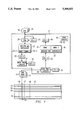
FIG. 1 illustrates, in simplified block diagram form, a peripheral data storage subsystem in which the present invention is employed together with a diagrammatic showing of a magnetic tape medium used in the subsystem.
FIG. 2 diagrammatically illustrates an original array of data bytes and error redundancies for the FIG. 1 illustrated system.
FIG. 3 illustrates a portion of the FIG. 1 illustrated magnetic tape medium for illustrating the effects of rotating rows of data within respective sets of the FIG. 2 illustrated array.
FIG. 4 illustrates, in simplified form, an block row rotator and array row interleaver for generating the format shown in FIG. 3.
FIG. 5 illustrates, in a simplified block form, a write channel of the FIG. 1 illustrated subsystem.
FIG. 6 illustrates, in a simplified block form, a read or reproducing channel of the FIG. 1 illustrated subsystem.
FIG. 7 illustrates, in a simplified flow diagram form, a de-rotator and de-interleaver of the FIG. 1 illustrated subsystem.
FIG. 8 illustrates in simplified logic form, a preferred block row rotator and array row interleaver for the FIG. 1 illustrated subsystem.
DETAILED DESCRIPTION
Referring now more particularly to the appended drawing, like numerals indicate like parts and structural features in the various figures. One or more host processors 10 attach a data storage subsystem that comprises peripheral controller 11 and a plurality of one-half inch high-performance magnetic tape drives 12. Each of the tape drives 12 can mount a tape-containing cartridge (not shown) having magnetic tape 13 for writing (recording) and reading(reproducing) operations. Each tape drive 12 has a multi-track multi-gap head or transducer assembly 15. Head assembly 15 can be constructed as shown in U.S. Pat. No. 5,161,299 by E. Dennison et al and assigned to IBM Corp. This patent shows deposited gaps and a gap array having a write gap and a read gap for each track to be scanned. The gap arrangement is alternated such that the head can write in either direction of relative tape movement. Each of the write gaps and read gaps simultaneously scan respective tracks, such as tracks 19 (not all tracks are shown) diagrammatically shown on tape 13. The number of tracks concurrently receiving data vary, in the illustrated embodiment from four to thirty-two tracks. That is, a number of tracks on a tape may vary from 32 to 128 or more, for example. On the 32 track tapes four tracks concurrently receive data for recording and yield data during reading. The larger the number of tracks on a tape in a higher performance recording system, the greater number of tracks concurrently receiving and yielding data. Numerals 16, 17 and 18 respectively indicate longitudinal boundaries of data recorded from one later-described created array shown in FIG. 2. Magnetic tape 13 may have more tracks 19 than read-write gap pairs on head 15. Head 15 is then movable laterally across magnetic tape 13 for accessing different groups of tracks, each group having a number of the write-read gap pairs for one direction of relative tape motion equalling the number of said gap pairs.
Random access memory (RAM) 20 receives and stores data, as detailed later with respect to FIG. 2, to be written on tape 13. During read operations RAM 20 stores data that has been successfully read from tape 13. Assume that data are to be written on tape 13. While such data are being stored in RAM 20, ECC-1 21 generates columnar error detecting and correcting redundancies for the data bytes in respective columns and stores the redundancies with the columns of data, as will become apparent. The RAM 20 stored data are moved to rotator and interleaver (RI) 23 for rearranging the data bytes as later described. The rotated and interleaved array data may be alternately stored in two RAMs bank 1 23-1 and bank 2 23-2. Then, the data to be recorded pass through ECC-2 circuit 22 for generating error detecting redundancies for each row of data in the created array. ECC-2 circuit 22 appends the generated redundancies to each row of data as the row passes to the write track circuits 24 for writing the data to the respective tracks. There is one write track circuit for each track to be written to.
In accordance with one aspect of this invention, RI 23 manipulates the data array for concurrently writing into either 4, 8, 16 or 32 tracks 19. Similarly, the later described read track circuits can recover data from tape 13 whether recorded in 4, 8, 16 or 32 tracks 19, provided of course that a suitable head assembly is provided.
Write track circuits respectively cooperate with ECC-3 circuits 25, one circuit 25 for each write track circuit, for adding a third ECC redundancy for each array row of data bytes that are recorded in a track, as will become apparent. Such redundancy enables error detection and correction in the respective recorded array rows. The data writing includes one or more created arrays of data for writing into portions 16-17, 17-18 etc. on tape 13. Each physical block of data written on tape 13, as later described, contains an integral number of such created data-ECC redundancy arrays.
Tape drive 12 reads data in a block (16-17) from tape 13. A set of read track circuits 30 receive the read signals from the reading tape drive 12. Circuits 30 detect the data in a known manner. One ECC-3 error detecting circuit 33 is attached to each of the plurality of read circuits 30. ECC-3 detects and corrects data errors in ones of the read array rows in the respective data sets. In the event ECC-3 detects but does not correct its detected data errors in the respective array rows, suitable pointer signals are sent to pointer circuit 97.
Following the ECC-3 data correction, each circuit 30 cooperates with ECC-2 error detecting circuits for detecting bytes in error in the respective block rows of data. Circuits 30 operate independently of each other, a small portion of each circuit 30 operates at a clock speed and phase slaved to the track being read, as is known.
Each of the circuits 30 supplies data from its respective detected set of data to de-rotate and de-interleave circuit (DI) 33. In a constructed embodiment, the data transfer was one data byte at a time. In DI circuit 33, the input addressing circuits for memory 34-35, uses address sequences for the various read circuits that de-rotate and de-interleave the data as data are stored into the memory 34-35 to create read or retrieved data array that is a replica of the original FIG. 2 illustrated data-ECC redundancy array. Deskewing between successive read arrays is achieved by storing the data in either bank 1 memory 34 or bank 2 memory 35 at the appropriate storage locations. DI circuit 33 cooperates with the read track circuits on a one-by-one basis. DI circuit 33 also de-commutates data from the read track circuits 30 to the memory banks 34 and 35, as will become apparent. As one bank, such as bank 1, fills with data, some of the read track circuits may finish reading data before other read circuits for bank 1 due to read data skew. At this time, as a deskewing operation, the early finishing read track circuits begin supplying data bytes from a second read array into bank 2. As soon as all of the read track circuits 30 finish supplying data to bank 1, bank 1 is full and ready for error detection and correction by ECC-1 circuit 36 (the outer code circuit).
Error pointers generated in read track circuits 30, as by detection of illegal recording code words, clock errors, ECC-2 and any ECC-3 generated error pointers are sent to be stored in ancillary buffers addressably associated with the read arrays such that ECC-1 circuit can access the read circuit generated error pointers for correcting bytes in error of each read array.
ECC-1 circuit 36 detects and corrects data errors in the read or retrieved array of data. The buffered error pointers are used to assist in the error correction, as is known. The corrected data are supplied to RAM 20 for transmittal to a data requesting host processor 10. Other circuits 39 in peripheral controller 11 represent all other circuits usually found in such a peripheral controller, such as host processor attachment circuits, timing circuits, control circuits of all types, etc.
FIG. 2 diagrammatically shows one created array 45 of data bytes and ECC redundancy bytes. One of these arrays are recorded as a unit in either 4, 8 or 16 concurrent tracks. For concurrent recording in 32 tracks, two arrays 45 are interleaved, as will become apparent. A greater number of concurrent tracks may be used in connection with practicing this invention. Array 45 consists of eight (8) blocks of data A-H. Such blocks A-H of data each can reside in respective portions of RAM 20 and are separately addressable in this manner. Each block of data has a plurality of block data rows R1-R32 and a plurality of data columns C1-C32. Column C33 is a phantom column as will become apparent for representing the ECC-2 error detecting (EDC) redundancy bytes. Each column-row intersection represents one byte of data. Therefore, each block row has 32 bytes of data while each column has 32 bytes of data. An array row consists of eight block rows, one block row from each of the blocks A-H having a same relative position constitutes an array row. That is, all of the block rows R1 in the blocks A-H constitute one array row.
Each intersection in the array 45 is identified by its column and row number, such as the upper left byte in block A is A-R1C1. Block rows are identified by block and row, that is A-R1 represents one block row of data. Columns are similarly identified as A-C1, etc. A range of rows is represented as A-R1 . . . R24, a range of columns is identified as A-C1 . . . C32. An array row is represented by R1-A . . . H, etc.
The data bytes to be stored in tape 13 are serially received from a host processor 10 are stored in RAM 20 in ranges A-R1C1 . . . R24C32 (a 24 high by 32 wide array of received data bytes). Each block A-H has host processor data stored in this range. The ECC-1 first or error correcting (ECC) redundancy bytes are in byte locations R25C1 . . . R32C32. Each of the columns C1 . . . C32 has a separate redundancy in rows R25 . . . R32 for the data in the respective columns C1 . . . C32 stored in rows R1 . . . R24. The second or inner code ECC-2 has redundancy error detecting bytes added after RI 23 rotates and interleaves the rows of data as later described. Such second redundancy is represented by column C33 in all rows R1 . . . R32. The ECC-3 created redundancies are not shown in FIG. 2. The ECC-3 redundancies are created for each array row (eight block rows).
As data bytes are serially received from a sending host processor 10, the bytes are stored in RAM 20 beginning at array location A-R1C1, then serially proceeding in the column A-C1 to A-R24C1. ECC-1 circuit processes each received data byte before each data byte is stored in RAM 20 such that as the last byte for column C1 is stored, the redundancy bytes are stored in byte locations A-R25C1 . . . R32C1. The data storage rate in RAM 20 is higher than the received rate.
The data byte storage in RAM 20 then proceeds to A-C2 for repeating the above-described procedure. This procedure is repeated for each column in each of the blocks A-H until a complete created array 45 is generated. At this point, the created array 45 is ready for further processing. RAM 20 may have sufficient data storage capacity and access rates for enabling creating a second array 45 whilst the above-described created array 45 is being further processed.
Before describing the further array 45 processing, a description is made of so-called set arrangements for storing created array 45 in tapes using a tape head 15 that may record and read concurrently from a diverse number of tracks. Each set of data is recorded bit serially in respective ones of the concurrent tracks. Table I below illustrates how the 256 rows of data bytes in created array 45 are arranged in respective sets for differing numbers of tracks. For 32 tracks, two arrays 45 are interleaved on tape 13 in each error detecting and correcting area of the data block, as will become apparent. The "*" indicates two arrays 45 in the table below.
              TABLE I
______________________________________
Number of
         Number of             Number of rows
concurrent
         block rows Number of  per block
Tracks   per set    sets       per track
______________________________________
 4       64          4         8
 8       32          8         4
16       16         16         2
 32*      16*        64*       2 ea array
______________________________________
The table above shows that the distribution of the rows by end-around rotation or shifting (see loop arrow 46 in FIG. 2) of block rows of data within array rows of each set distributes the block rows evenly across and longitudinally of the tape for a maximal physical spacing between the rows of data bytes in a minimal area. Such even spatial distribution of the data reduces the number of data errors for one tape caused error (surface defect, for example or debris on the tape) thereby reducing the number of data errors in each of the columns of data in the non-rotated non-interleaved array. Such data error reduction enhances the error detection and correction.
The table below is an abbreviated showing of the row distribution in a concurrent 16-track recording.
              TABLE II
______________________________________
                       Row sequence
Track number
          First Block Row
                       16 rows per track
______________________________________
1         A-R1         A-R1..H-R1
                       A-R2..H-R2
2         B-R3         B-R3..H-R3,A-R3
                       B-R4..H-R4,A-R4
3         C-R5         C-R5..H-R5,A-R5,B-R5
                       C-R6..H-R6,A-R6,B-R6
4         D-R7         D-R7..H-R7,A-R7..C-R7
                       D-R8..H-R8,A-R8..C-R8
5         E-R9         E-R9..H-R9,A-R9..D-R9
                       E-R10..H-R10,A-R10..D-R10
6         F-R11        F-R11..H-R11,A-R11..E-R11
                       F-R12..H-R12,A-R12..E-R12
7         G-R13        G-R13,H-R13,A-R13..F-R13
                       G-R14,H-R14,A-R14..F-R14
8         H-R15        H-R15,A-R15..G-R15
                       H-R16,A-R16..G-R16
9         A-R17        A-R17..H-R17
                       A-R18..H-R18
______________________________________
Table II can be completed for tracks 10-16 by adding 16 to the track numbers 1-8 and 16 to each of the row values in the other two columns. Other tables can be similarly created for different numbers of concurrently recorded tracks.
FIG. 3 illustrates a partial format of a 16-track recording on tape 13. Tracks 19-1 and 19-2 are diagrammatically partially shown. Track 19-1 is track number one that stores the first set of rows as shown in Table II. The figure assumes that all other recording controls have been processed, i.e. a read clock is in sync and byte boundaries have been identified in a usual manner. Rows A-R1 and B-R1 are written in track section 50 (a total of 66 bytes) followed by a so-called byte resync indicator 51 of known design. Then next track section 52 stores rows C-R1 and D-R1. Byte resync 53 follows track section 52. Then track section 54 storing rows E-R1 and F-R1 precedes third byte resync pattern 55. Then track section 56 stores rows G-R1 and H-R1 followed by the ECC-3 redundancy in track section 57. In this instance ECC-3 detects errors in an array row of data A . . . H-R1. Byte resync 58 is disposed between ECC-3 redundancy at 57 and a next eight block rows in area 59 of track 19-1. Track 19-1 contains block rows A-R2 . . . H-R2 (one array row A . . . H-R2) using the same format for sections 50-58 including the ECC-3 and the byte resync's. Similarly, track 19-2 includes the resync patterns 51, 53, 55 and 58 for separating rotated block row pairs B-R3, C-R3 in section 65, D-R3, E-R3 in section 66, F-R3, G-R3 in section 67 and H-R3, A-R3 in section 68.
An ECC-3 redundancy is recorded in section 69. Area 70 stores the last block rows in the track 19-2 set of rows, as listed in Table II. All other tracks are similarly formatted. A concurrent 32-track recording interleaves two arrays 45 as later described.
FIG. 4 shows, in simplified form, RI 23 for rotating and interleaving the rows of a data array for up to sixteen concurrent tracks. A preferred constructed embodiment of RI 23 is shown in FIG. 8. Address decoder 77 supplies each byte address to RAM 20. Decoder 77 further arranges the later-described count values to the addressing arrangement of RAM 20, as is known. Byte counter 81 counts the bytes in each of the rows of array 45, i.e. generates the least significant digits of the address. Block counter 82 counts the blocks A-H, hence is a modulo 8 counter. Counter 83 counts the rows in each set. Block counter 82 cycles once for each count of row counter 83. REP circuit 84 indicates to block counter 82 the block number that is to start and end each set, i.e. solves the rotation formula. That is, block counter 82 may start at 1, 2, etc. depending on which of the blocks A-H are to supply the first row in a set. Array counter 85 is a one bit counter for the 32-track recording operations.
Cycler 86 steps the counters 81-85 and supplies a signal to RAM 20 for readout to the respective write track circuit indicated by track counter 89. Track counter cycles through the track numbers for selecting the write track circuit. Track counter also supplies the track number to the block counter 82 and row counter 83 for solving the respective formulae. The number of tracks being recorded is indicated in TRACKS circuit 88. Circuit 88 controls the modulus of counter 89, REP circuit 84 and array counter 85 (on or off).
A concurrent 32-track recording interleaves two arrays 45 in any one of several interleave patterns. Such array interleaving records like array sets in each track, that is track 1 receives a first array set from both arrays, track 2 receives a second array set from both arrays, etc. The array interleaving alternates such array sets from the two arrays in the data tracks between a first or leading position and a second or trailing position in each track. If it is desired to provide the interleaving alternation on a track-by-track basis, then a first data array has its sets in the first position in all odd numbered tracks while a second data array has its sets in the even numbered tracks. The array sets are reversed for the second or trailing position in the tracks. Array register 85 is a one bit register that is toggled each time the indicated array rows of a leading array have been sent to the write track circuits. Such toggling selects a different array portion of RAM 20, for example. The operation of RI 23 alternates between the arrays, each cycle of interleaving and rotating the indicated array rows is repeated for the trailing array.
Such array rows from two created arrays 45 (array 1 and array 2) can be interleaved in an alternate leading and trailing locations in the respective groups of any arbitrary number of tracks. For example, groups of eight tracks may be selected. In any 32-concurrent track recording, a integral number of the two-array interleaved data constitute a data block.
Line 178 carries a 32-concurrent-track indicating signal from other circuits 39 for controlling array register 85 to toggle its value between array 1 and array 2 as indicated above. Further, the block counter 82 and row counter 83 repeat their respective counts for array 1 and array 2. Two counters may be used, one for array 1 and one for array 2. In this illustration, one array, array 1 or array 2 is processed at a given instant.
FIG. 5 shows, in simplified form, a write track circuit.
Table III below illustrates how two created arrays are interleaved and recorded on a 32-track tape.
              TABLE III
______________________________________
ARRAY               ARRAY ROW     TRACK
SEQUENCE    LEAD    LAG           NUMBER
______________________________________
odd         1       2             odd
odd         2       1             even
even        2       1             odd
even        1       2             even
______________________________________
Table III shows the alternation of data from arrays 1 and 2 in the odd and even numbered tracks. The lead column indicates which array supplies a row of data as a first or lead recorded data while the lag column lists the second or lagging recorded data source. The track number column indicates track numbers as being either odd or even. The ARRAY SEQUENCE column indicates the above-described alternation (odd and even) of array 1 and array 2.
Gate 100 receives data from RAM 20 and a TRACK N signal from counter 89 (FIG. 4) for passing the RAM 20 data to buffer 101. ECC-3 circuit 102 adds the ECC-3 redundancy to the data as it passes through buffer 101. Circuit 103 adds the usual medium control signals, such as a block preamble, byte resync and the like. Digital modulation circuit 104 encodes the data into a digital modulation or recording code, such as a 1,7 d,k code for recording on tape 13 via head 15. The usual analog amplifiers, etc. are not shown. Write track circuits operate identically irrespective of the number of concurrent tracks.
FIG. 6 is a simplified showing of a read track circuit 30. The one track read signal (not shown) from head 15 travels through the usual read circuits 90 for amplification, compensation and detection including converting a d,k recording code to NRZ data signals. ECC-3 circuit 102 processes the read data for detecting and correcting short errors in the array row portions of each read set. Detected errors are indicated to pointer circuit 97 for later transmission to a pointer memory (FIG. 7). ECC-3 circuit may have error correction capability for correcting up to two bytes in error. Similarly, ECC-2 circuit 92 processes the read data for detecting errors in the respective rows, there being one error detecting redundancy for each row. Detected errors in a row are supplied to a separate latch in pointers circuit 97 to await transmission to ECC-1 circuit 36. The read data then is de-serialized into byte buffer 93. As soon as one data byte is stored in buffer 93, ready latch 95 is set to the active condition for signalling DI circuit 33 that a byte of data is ready to be transmitted. DI circuit responds to the line 96 ready signal by sending read-out signal over line 132 to buffer 93 for transferring one byte of data to DI circuit 33 and to reset latch 95 to the not-ready state. Except for addressing as shown in FIG. 7, read track circuits 30 operate identically irrespective of the number of concurrent tracks.
Read circuits 90 may detect an error in the d,k read signals. Such detected errors are indicated to pointers circuit 97 for temporary storage and transmission to ECC-1 circuit 36 with the row of data signals, as will become apparent. Each of the three types of pointers are separately stored in pointers circuit 97. Pointer circuit 97 having one pointer stored therein supplies the one-bit pointer signal over line 98 to DI 33. DI circuit 33 reads the pointer signal and supplies a reset signal over line 141 for resetting the pointer bit latches(not shown).
DI circuit 33 is best seen in FIG. 7. DI 33 includes one address generation circuit 115 for each of the read track circuits 30. In a 16-track read operation, there are 16 active address generation circuits 115, each such circuit having an fixed sequence of address generation for de-rotating and de-interleaving the data bytes for each respective track, such as set forth in the tables above. Each circuit 115 includes a fixed sequence counter 116 for counting the data byte transmission from its circuit 30 to memory 34-35. The address generation is created by track counter portion 120 that is set to a fixed value, row counter 121 that counts the rows to which the read data bytes are to be transmitted, rotation counter 122 that adjusts the block counter 123 to start counting at a respective one of the blocks A-H and column counter 124 that counts the byte locations (columns) in the read or retrieved array being generated in memory 34-35.
Scanner 130 continuously scans, at high speed, the ready latches 95 for finding filled byte buffers 93. The scan is round robin. A first detected ready latch 95 in the ready condition interrupts the scanner 130. Scanner 130 responds by activating the respective address generation circuit 115 for generating a next address for memory 34-35. Simultaneously, scanner 130 supplies a buffer read signal over the respective buffer read line 132 for actuating the respective byte buffer 93 to supply its stored byte of data over bus 94 to memory 34-35 for storage in the byte location indicated by the respective address circuit 115.
Pointers stored in read track circuits 30 are indicated to pointer scanner 140. Scanner 140 senses the pointer ready signal on the line 98 (one pointer is active). Pointer scanner 140 then sends a pointer read signal over the respective line 141 to pointer memory 111 for receiving the pointers and to clear the pointers circuit 97. If no pointer is present, then pointer memory receives no signal. Each of the lines 98 is directed to a three bit register, one bit for each of the pointers. Memory 111 supplies the stored pointer signals to ECC-1 circuit 36.
Pointers are sent to ECC-1 circuit 36 whether zero (no error) or one (error). As soon as bank 1 or bank 2 of memory 34-35 is full and the error pointers are in ECC-1 circuit, ECC-1 circuit reads the data from the respective memory bank. The addresses that the pointers are stored in memory 111 are logically associated with the data in memory 34-35 in a usual manner. Pointer memory 111 has one portion for each of the banks 1 and 2. Therefore, as bank 1 is being read by ECC-1 circuit 36 the bank 2 pointers are being stored into pointer memory 111 all under control of bank select portion of address decoder 110.
Line 178 from other circuits 39 carries a 32-track signal for indicating that 32 concurrent tracks are being read. While line 178 carries an indication of other than 32 concurrent tracks, then the above-described operation occurs, i.e. one retrieved array is being generated. For 32 concurrent tracks two retrieved arrays are generated by de-interleaving the two arrays being read from tape 13. Array selector 177 responds to the line 178 signal indicating 4, 8 or 16 concurrent tracks to emit a no-action signal over line 188 to always select the above described elements to process array 1. Array selector 177 responds to the line 178 signal indicating 32 concurrent tracks and to sequence counter 116 indicating that one set of data from one array has been read from respective ones of the tracks and activating signal over line 188 for toggling later-described controls to switch processing from either array 1 to array 2, or vice versa. Each of the address generation circuits 115 include two address circuits. The address elements 120-124 constitute a first address circuit used for processing array 1 while numeral 200 indicates a second address circuit, identical to elements 120-124, for generating addresses to process array 2. While array selector 117 is emitting an active signal, array 2 is being processed such that sequence counter 116 increments address circuit 200. Similarly, the line 188 active signal selects a second pointer memory 111-A and second memory 34-A. Address decoders 110 and 110-A are similarly selected respectively for processing array 1 or array 2. When either array 1 or array 2 have been completely read, ECC-1 processes the error pointers and data in a usual manner.
The three ECC codes may use the following generator polynomials:
For ECC-1:
G(X)=X.sup.8 +α.sup.176 X.sup.7 +α.sup.240 X.sup.6 +α.sup.211 X.sup.5 +α.sup.253 X.sup.4 +α.sup.220 X.sup.3 α.sup.3 X.sup.2 +α.sup.203 X+α.sup.36
For ECC-2 (error detection only):
G(X)=X+α
For ECC-3 (error detection and correction):
G(X)=X.sup.4 +α.sup.74 X.sup.3 +α.sup.247 X.sup.2 +α.sup.75 X+α.sup.2
where GF(256) is constructed using a primitive polynomial
P(x)=X.sup.8 +X.sup.3 +X.sup.2 +X+1
for all three generator polynomials.
The primitive element α=00000001 in the three generator polynomials.
FIG. 8 illustrates in simplified form a preferred interleaver logic arrangement for efficiently providing diverse track interleaving. The theory for RI 23 is based on the three-dimensional showing of FIG. 2. The interleaver uses the three ordinates X, Y and Z. Ordinate X indicates the horizontal offset or column number (enumerated 0-31 rather than 1-32), ordinate Y indicates the vertical offset or row of data bytes (enumerated 0-31 rather than 1-32) and ordinate Z is the depth ordinate or the block address A-H (enumerated 0-7). The row rotation or shifting within set is determined by a modulo-8 adder.
Table IV below illustrates the calculation of the X, Y and Z data array offsets that lead to a linear memory address for RAM 20 that simultaneously effects the interleaving and row rotation or end-around shifting of block rows within each array row.
              TABLE IV
______________________________________
Number of                        Z offset
concurrent
        X offset    Y offset     block number
tracks  column number
                    row number   modulo 8
______________________________________
4       Column number
                    (8*TRK)+ROW  2*TRK + BLK
8       Column number
                    (4*TRK)+ROW  TRK + BLK
16      Column number
                    (2*TRK)+ROW  TRK + BLK
______________________________________
In Table IV, TRK indicates a Y-offset in a data array representing which group of eight block rows are being addressed, BLK means the block number 0-7 respectively to address blocks A-H and ROW indicates the block in which a row is to be read within an array row. The RAM 20 buffer address is calculated using the equation below:
Address=(Z*1024)+(X*32)+Y (1)
The modulus of the values TRK and ROW vary with the number of concurrently recorded tracks. The data row byte address is a constant 5-bit quantity while the BLK value (selects a block A-H using an address value of 0-7) has a constant modulus of 3 bits. The ROW modulus for four concurrent tracks is three bits, two-bits for eight concurrent tracks and one bit for 16 concurrent tracks.
The FIG. 8 illustrated address-mapping logic calculates the X, Y and Z data array values for insertion into 13-bit address register 150. The RAM 20 address consists of the Y offset as the five lowest significant bits 8-12 received through Y multiplexor 151, the middle significant bits 3-7 as the X offset via X multiplexor 165 and the highest order bits 0-2 from the modulo 8 Z offset adder 160. A thirteen-bit counter 170 cycles once to create the RAM 20 addresses for one of the created arrays 45. Counter 170 has thirteen output lines 171 that are connected to the inputs of the address-mapping logic as shown below in TABLE V.
              TABLE V
______________________________________
counter  input line numbers to address-mapping logic
output Line
         4-track input
                     8-track input
                                 16-track input
number   line number line number line number
______________________________________
0        175-Y2      177-Y3      180-Y4
1        175-Y3      177-Y4      192-B0
2        175-Y4      191-B0      192-B1
3        190-B0      191-B1      192-B2
4        190-B1      191-B2      197-C0
5        190-B2      196-C0      197-C1
6        195-C0      196-C1      197-C2
7        195-C1      196-C2      197-C3
8        195-C2      196-C3      197-C4
9        195-C3      196-C4      181-Y0
10       195-C4      185-Z0 &    186-Z0 &
                     178-Y0      181-Y1
11       176-Y0 &    185-Z1 &    186-Z1 &
         184-Z0      178-Y1      181-Y2
12       176-Y1 &    185-Z2 &    186-Z2 &
         184-Z1 &    178-Y2      181-Y3
         184-Z2 = 0
______________________________________
In TABLE V, the term Y means vertical ordinate or row number (R1-R32; 0-31), B means block A-H (0-7), T means track number, and C means column number for indicating a byte in each of the rows.
For processing a 32-track concurrent recording, a second byte counter 170-A and multiplexor 172 is added. The line 178 signal controls counters 170 and 170-A to respectively increment whilst array 1 and array 2 are being processed, as shown in TABLE III, above, in the array row column. Multiplexor 172 responds to the line 175 signal from either counter 170 or 170-A reaching the trigger count for switching processing between array 1 and array 2. The lines 171 have connections as above described.
While the invention has been particularly shown and described with reference to preferred embodiments thereof, it will be understood by those skilled in the art that various changes in form and details may be made therein without departing from the spirit and scope of the invention.