US5107140A - Anticipatory automatic gain control circuit - Google Patents
Anticipatory automatic gain control circuit Download PDFInfo
- Publication number
- US5107140A US5107140A US07/430,502 US43050289A US5107140A US 5107140 A US5107140 A US 5107140A US 43050289 A US43050289 A US 43050289A US 5107140 A US5107140 A US 5107140A
- Authority
- US
- United States
- Prior art keywords
- signal
- amplitude
- gain
- input
- input signal
- Prior art date
- Legal status (The legal status is an assumption and is not a legal conclusion. Google has not performed a legal analysis and makes no representation as to the accuracy of the status listed.)
- Expired - Lifetime
Links
Images

Classifications
-
- H—ELECTRICITY
- H03—ELECTRONIC CIRCUITRY
- H03G—CONTROL OF AMPLIFICATION
- H03G3/00—Gain control in amplifiers or frequency changers without distortion of the input signal
- H03G3/20—Automatic control
- H03G3/30—Automatic control in amplifiers having semiconductor devices
-
- H—ELECTRICITY
- H03—ELECTRONIC CIRCUITRY
- H03K—PULSE TECHNIQUE
- H03K5/00—Manipulating of pulses not covered by one of the other main groups of this subclass
- H03K5/01—Shaping pulses
- H03K5/02—Shaping pulses by amplifying
-
- H—ELECTRICITY
- H03—ELECTRONIC CIRCUITRY
- H03K—PULSE TECHNIQUE
- H03K5/00—Manipulating of pulses not covered by one of the other main groups of this subclass
- H03K5/01—Shaping pulses
- H03K5/08—Shaping pulses by limiting; by thresholding; by slicing, i.e. combined limiting and thresholding
- H03K5/082—Shaping pulses by limiting; by thresholding; by slicing, i.e. combined limiting and thresholding with an adaptive threshold
Definitions
- This invention relates to an automatic gain control circuit and, more particularly, to an anticipatory automatic gain control circuit for use with a bar code scanner.
- a bar code reader typically uses a beam of light to read a bar code, which consists of alternating strips ("bars") of differing reflectivities. The scanner then receives and interprets the fluctuations in the returning light that are caused by the bar code. It is known in the prior art to read bar codes by means of a hand-held wand which makes contact with the surface on which the bar code is printed. However, the need to make contact with the surface is frequently inconvenient and gives uninterpretable readings because the wand is not moved across the bar code with a sufficiently uniform velocity.
- a bar code scanner typically produces a beam of light which is repetitively scanned across an area.
- the beam of light can be produced by a laser source, such as a laser diode. If the beam of light intercepts a bar code (or some other symbology), the modulated light which is reflected by the bar code is returned to sensing circuitry in the bar code scanner for interpretation.
- the strength of the modulated light signal is a function of the reflectances of the bars and spaces in the bar code, and the distance between the scanner and the bar code.
- the intensity of the received signal also varies widely.
- the wave shaper converts the received signal into a digital pulse train
- This circuitry requires a signal of well controlled amplitude.
- These laser scanners also incorporate circuitry to either adjust the level of the signal to fit the wave shaper automatic gain control (AGC), or adjust the operation of the wave shaper to fit the signal (adaptive wave shaping).
- AGC automatic gain control
- the received signal is analyzed on the basis of relative time. That is, the widths of the alternating areas of different reflectivity are measured on the basis of their relative scanning times. This allows the reader to be used with bar codes which have a wide variety of sizes, the important factor being that the relative widths of the elements of the bar codes be preserved. Accordingly, it is preferable that the light beam be scanned across the bar code at a substantially uniform rate in order to ease the task of interpreting the bar code.
- AGC circuit for a laser scanner is complicated by several conflicting requirements.
- the gain must be adjusted to maintain a constant output signal level independent of the input signal level.
- noise from various sources will be amplified to the point that it will produce a random output signal.
- the circuitry of the scanner will be forced to try to decode this random output signal, making the laser scanner slower in interpreting bar codes.
- scanners require a "quiet zone" on either side of the bar code. If the gain stays at its maximum through the quiet zone and up to the start of the bar code, noise in the quiet zone may cause spurious digital output pulses which obscure the beginning of the bar code. This problem requires that the maximum available gain be limited to a value which will prevent noise from being detected by the wave shaper.
- the AGC circuit must respond extremely rapidly to any change in its input signal. That, however, causes the AGC circuit to track every variation in the input signal. This results in a gain control signal which varies as rapidly as the input signal, causing severe distortion. To avoid such distortion, while maintaining the fast response to the start of the bar code, it is necessary to make the AGC time constant highly asymmetrical.
- the AGC circuit must respond instantaneously to an increase in the signal level, but must respond only very slowly to a decrease in the signal level. Thus, once the gain is reduced, it can only be increased slowly.
- the invention is an anticipatory automatic gain circuit for anticipating a gain.
- the gain is that required to amplify a pulsed input signal having an amplitude which varies between input minimum and maximum values and to produce an output signal having an amplitude between predetermined minimum and maximum values.
- the amplitude of the output signal corresponds to the amplitude of the pulsed input signal.
- the anticipatory automatic gain circuit comprises means for producing a delayed pulsed input signal having an amplitude which varies between the input minimum and maximum values. It also comprises means for comparing the amplitude of the input and delayed input signals and producing a peak detection signal which represents the amplitude of the input and delayed input signals, whichever is greater.
- the circuit comprises first and second variable-gain amplifier means and automatic gain control detector means.
- the first variable gain amplifier means amplifies the peak detection signal to produce an amplified peak detection signal in response to a control signal.
- the automatic gain control detector means detects the amplitude of the amplified peak detection signal and produces the control signal.
- the second variable gain amplifier means amplifies the delayed pulsed input signal to produce the output signal in response to the control signal.
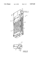
- FIG. 1 is a perspective diagram of a scanning laser bar code reader.
- FIG. 2 is an end-on view of the top end of the scanning laser bar code reader shown in FIG. 1.
- FIG. 3A is a first part of a schematic diagram of signal conditioning circuitry for a scanning laser bar code reader, including an anticipatory gain circuit.
- FIG. 3B is a second part of a schematic diagram of signal conditioning circuitry for a scanning laser bar code reader.
- This invention is based on the premises that it is not necessary to predict the future in order to produce an anticipatory AGC circuit. Remembering the past is equally effective.
- FIG. 1 is a perspective diagram of the laser scanner.
- FIG. 2 is an end-on view of the top end of the laser scanner shown in FIG. 1.
- the laser scanner 10 contains electronic circuitry and optical components contained within a case 12. It includes a keyboard 14 and liquid crystal display (LCD) 16 for the display of bar codes which have been read by the laser scanner 10 as well as for programming a microprocessor (not shown) contained within the laser scanner 10.
- LCD liquid crystal display
- the laser scanner 10 Upon actuating a pair of opposed trigger switches 18 (one shown in FIG. 1; also see FIG. 3B), the laser scanner 10 is activated to produce a scanning beam (not shown) of laser light.
- the scanning beam passes through the window 20 placed in the top end of the laser scanner 10, as shown in FIG. 2.
- the scanning occurs in the plane 22 (shown in FIG. 2).
- the light from the scanning beam is projected forwardly of the laser scanner 10. If it reaches a surface, some of the impinging energy returns to the window 20. If the reflecting surface happens to contain bar code symbology which the scanning laser beam impinges upon, the returning light will be modulated by the pattern of reflectivities which the bar code symbology contains.
- the light received by the laser scanner 10, if it is reflected from a bar code symbology can be amplified and processed by circuitry that will be described in greater detail subsequently.
- the wavelength of the light beam of laser light produced within the laser scanner 10 is determined by the laser light source which is contained in the laser scanner 10.
- the laser light source can produce a wavelength beyond the range of human vision ("invisible”) or a wavelength within the range of human vision (“visible”). If an invisible laser beam is used to read the bar code symbology, it will generally be necessary to include an auxiliary light beam to be used by the operator of the laser scanner 10 to place the scanning beam on the bar code symbology.
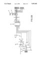
- FIGS. 3A and 3B are first and second parts of a schematic diagram of signal conditioning circuitry for a scanning laser bar code reader, including an anticipatory gain circuit.
- the circuitry shown in the schematic diagrams of FIGS. 3A and 3B contain a 500 kHz clock 21, a power supply 23, control logic 24, a motor motion detector circuit 26, and a waveshaper 28.
- the 500 kHz clock 21 is a simple CMOS gate-type oscillator. Its output drives an analog time delay element 30 (to be discussed subsequently) and a -5 volt power supply inverter 32. Both are driven by the same clock so that any clock-frequency noise coupled into the time circuitry ahead of the analog delay element 30 will by synchronously sampled within the time delay element 30 and converted to a DC offset at its output. The DC offset, accordingly, can be ignored.
- the time delay element 30 requires that the clock which drives it be centered approximately 2.5 volts above the supply voltage Vss.
- Capacitor 34 and resistors 36 and 38 provide the level-shifting function.
- the wave shaper and other circuitry requires a -5 volt power supply. It is important that this supply have good efficiency and low noise, as well as using as few components as possible.
- the -5 volt power supply used is designed to maintain regulation over a load range of 5 to 40 mA. The typical load on the -5 volt power supply is 15 mA.
- the -5 volt power supply contains a pulse-width modulator derived from the 500 kHz clock, a high-speed switch, an output filter, and an error amplifier 39.
- Circuitry in the power supply 23 generates a ramp waveform from the square 500 kHz clock.
- the ramp has a slow positive-going edge, whose rise rate depends on the output of the error amplifier 39.
- the fall time of the ramp is independent of the control signal. This is readily understood by observing that capacitor 40 is charged through transistor 42, which acts as a controlled current source, and is discharged through diode 44.
- transistor 54 When transistor 54 is on, 5 volts are applied across inductor 56. This causes the current in inductor 56 to increase from 0 amperes to a value dependent upon how long transistor 54 is left on. When transistor 54 turns off, the current in inductor 56 cannot rapidly return to 0, but rather it keeps flowing in the same direction as it did when transistor 54 was on, but now it must flow through diode 58, a fast, low-loss Schottky diode, charging capacitors 60 and 62 to a negative voltage. If for some reason transistor 54 is on continuously, the current will increase to the point that either transistor 54 or inductor 56 will burn up.
- the error amplifier 39 compares the -5 volt output (via resistor 64) to the +2.5 volt reference (via resistor 66), integrating the result with capacitor 68 and applying the error signal to the pulse-width modulator previously described, thus regulating the output voltage.
- the motor motion detector circuit 26 has been incorporated.
- the operational amplifier 70 in that circuit monitors the voltage across one of the motor windings (on line 72).
- the operational amplifier 74 compares that to a fixed reference level (on line 76).
- the control logic 24 only samples the comparator output 78 during the time when the monitored winding is not being driven.
- the waveshaper 28 is intended to convert the analog waveform representing the light intensity scattered from the bar code as it is scanned by the laser beam into a digital waveform representing as accurately as possible the actual bar space of the bar code.
- Diode 84 clamps the large spikes which result from a direct reflection of the laser beam off a shiny surface and into the detector. This prevents saturation and slow recovery of anticipatory AGC circuit 110.
- the waveshaper 28 shown in FIGS. 3A and 3B is of the type known as a double differentiator. It detects bar code edges based on points where the second derivative of the input signal is zero. It is called a double differentiator because it finds changes in concavity of steep sections of the input signal 80. In other words, the waveshaper 28 finds places where the second derivative of the input signal is zero (signal slope is unchanging) while the first derivative is large (slope is steep).
- the circuit 82 between the input signal 80 and the time delay element 30 is a combination differentiator, amplifier, and low-pass filter. Its response characteristic has one zero at 0 Hz and one complex pole pair at 40 kHz. Thus circuit 82 behaves as a differentiator for moderate frequencies, but rapidly rolls off at frequencies above those present in a bar code. In a double differentiator circuit, it is necessary to remove all high frequency components above the band of interest or they will be greatly exaggerated by the differentiator's high-pass characteristic.
- the AGC circuit described below is not limited to use with a double differentiator or any other specific kind of waveshaper 28. In fact, although it is discussed in the context of a laser scanner, the AGC circuit of the invention need not be limited to use with a bar code scanner.
- the new anticipatory AGC circuit 110 (see FIG. 3A) has several distinct advantages over the fast-attack, slow-release type used in the prior art. It preserves the sanctity of the quiet zone by reducing the gain well ahead of the arrival of the bar code signal. It is immune to being blinded by bright reflections. So long as the reflection occurs away from the actual bar code, there will be no recovery period. Within the bar code, it presents a smoother gain variation characteristic than AGC circuits in the prior art, causing less signal distortion.
- the main elements in this circuit are the time delay element 30, a matched pair of variable-gain amplifiers 122 and 124, a pair of precision rectifiers 126 and 128, and an AGC detector/comparator/integrator circuit.
- the operation of the anticipatory AGC circuit 110 is as follows:
- the input signal 80 is applied to the input of the time delay element 30.
- the time delay element 30 is a bucket brigade device.
- delay elements such as SAW devices, transmission lines and magnetic tape loops, which could also be used.
- the delay is 2 milliseconds.
- a suitable clock for use with this time delay element operates at a rate of 500 kHz.
- a band-pass filter consisting of resistors 130 and 131 and capacitors 132 and 133 filters out any fast variations in the output of the time delay element 30 as well as the DC offset component of the signal.
- the pair of precision rectifiers 126 and 128 is connected to the time delay element 30, one to the input 144 and one to the output 146 of the time delay element 30.
- the rectifiers' outputs are tied together at point 148 to produce a signal which measures the larger of the two signals.
- This envelope signal at point 148 includes the envelope of the delayed signal, but combines it with the envelope of the original signal as well. Put another way, the envelope signal at output 148 anticipates the signal at output 146 by 2 milliseconds.
- the envelope signal at point 148 is amplified by amplifier 122, one of the two variable-gain amplifiers.
- the peak of the output of that amplifier (at point 150) is compared to a reference voltage 151 in the AGC detector circuit 152. If it exceeds the reference, a control signal 154 is generated via a high gain integrator 153. This control signal is transmitted to the variable-gain amplifier 124, where it reduces the gain until the amplitude of the amplified signal is equal to the reference voltage 151.
- Each variable-gain amplifier 122 and 124 contains an op-amp connected as a non-inverting amplifier where the feedback resistor has been replaced by a transconductance amplifier.
- the transconductance amplifier is an integrated circuit whose output current is equal to its differential input voltage multiplied by a transconductance which is proportional to a control current.
- the output of the variable-gain amplifier 122 (at point 150) is used only for comparison to the reference voltage 151.
- the second variable-gain amplifier 124 is connected to the output of the time delay element 30.
- the control voltage 154 is applied to the second variable-gain amplifier 124 as well as the first variable-gain amplifier 122. Since the control voltage 154 is identical, and the variable-gain amplifiers 122 and 124 are identical, the gain of the second variable-gain amplifier 124 is the same as that of the first variable-gain amplifier 122. Accordingly, the amplitude of the output signal 156 will also equal the reference voltage 151 even though there is no feedback around the second variable-gain amplifier 124 to force its output to equal the reference voltage 151.
- the first variable-gain amplifier 122 and AGC loop 160 looking at the envelope signal at point 148 will force the gain down as soon as a large signal enters the time delay element 30.
- the gain of the second variable-gain amplifier 124 will be reduced at the same time as the first variable-gain amplifier 122. However, that is 2 milliseconds before the signal at output 146 comes out of the time delay element 30.
- the anticipatory AGC circuit 110 has anticipated a coming change in input signal level and adjusted its gain in advance.
- the anticipatory AGC circuit 110 also includes filtering.
- the gain control input 154 to the second variable-gain amplifier 124 is low-pass filtered. This is done because the AGC loop around the first variable-gain amplifier 122 has a fast attack time, resulting in a somewhat jagged control voltage 154.
- the low-pass filter on the gain control input of the second variable-gain amplifier 124 smooths out the jaggedness, reducing AGC-induced distortion of the output signal 156.
- the other filtering in the anticipatory AGC circuit 110 is to eliminate signals outside of the frequencies corresponding to the bar code, stabilize the variable-gain amplifiers, and reduce the noise generated by the sample-data nature of the delay line.
- the output of the second variable-gain amplifier 124 is passed through an inverted low-pass filter 86.
- the filter output represents the final "cleaned up” version of the first derivative of the analog signal.
- An edge detector 88 uses two sets of comparators 90A-D with their open-collector outputs wire-ANDed together, driving a set-reset flip-flop (not shown) to determine the bar/space transitions.
- Capacitor 92 and resistor 94 form the second differentiator. Their output is compared to zero by the upper two comparators 90A and 90B. The output of comparator 90A goes high if the second derivative is negative. The output of the comparator 90B goes high if the second derivative is positive. The second derivative zero level is offset to +2.5 volts to allow the comparators 90A and 90B to run on a single-ended +5 volt supply.
- the lower two comparators 90C and 90D determine whether the first derivative signal is large enough to enable the transitions detected by the second derivative comparators 90A and 90B.
- the signal is compared directly to a DC voltage generated from the +2.5 volt reference via a voltage divider.
- the single-ended comparator power supply requires that the signal level be offset in a positive direction such that 0 volt represents the allowable threshold level.
- the anticipatory AGC circuit 110 also incorporates provision for limiting the maximum achievable gain. It does this by adding a third precision rectifier 170, connected to a fixed voltage 172, to the envelope detector section by connecting its output 174 to the point 148 which is input to the first variable-gain amplifier 122.
- the envelope output at point 148 is always the larger of either the voltage on the input 144 of the time delay element 30, the voltage on the output 146 of the time delay element 30, or the fixed DC gain-limiting voltage.
- the voltage 174 presents a non-zero output at point 148 to the first variable-gain amplifier 122, causing the AGC loop to increase the gain only to the point that the output of the first variable-gain amplifier 122 is equal to the reference voltage 151.
Abstract
Description
Claims (5)
Priority Applications (1)
| Application Number | Priority Date | Filing Date | Title |
|---|---|---|---|
| US07/430,502 US5107140A (en) | 1989-10-31 | 1989-10-31 | Anticipatory automatic gain control circuit |
Applications Claiming Priority (1)
| Application Number | Priority Date | Filing Date | Title |
|---|---|---|---|
| US07/430,502 US5107140A (en) | 1989-10-31 | 1989-10-31 | Anticipatory automatic gain control circuit |
Publications (1)
| Publication Number | Publication Date |
|---|---|
| US5107140A true US5107140A (en) | 1992-04-21 |
Family
ID=23707816
Family Applications (1)
| Application Number | Title | Priority Date | Filing Date |
|---|---|---|---|
| US07/430,502 Expired - Lifetime US5107140A (en) | 1989-10-31 | 1989-10-31 | Anticipatory automatic gain control circuit |
Country Status (1)
| Country | Link |
|---|---|
| US (1) | US5107140A (en) |
Cited By (6)
| Publication number | Priority date | Publication date | Assignee | Title |
|---|---|---|---|---|
| US5168148A (en) * | 1990-12-28 | 1992-12-01 | Symbol Technologies, Inc. | Automatic gain control circuit |
| US5463603A (en) * | 1992-03-18 | 1995-10-31 | Imp, Inc. | Computer disk drive integrated data path circuit optimized for handling both data and servo signals |
| US5825008A (en) * | 1996-03-08 | 1998-10-20 | Eastman Kodak Company | Apparatus and method for setting radial bar code disc sensor gain in a phtographic camera |
| US6037809A (en) * | 1998-06-02 | 2000-03-14 | General Electric Company | Apparatus and method for a high frequency clocked comparator and apparatus for multi-phase programmable clock generator |
| US6417730B1 (en) | 2000-11-29 | 2002-07-09 | Harris Corporation | Automatic gain control system and related method |
| US20150364161A1 (en) * | 2014-06-16 | 2015-12-17 | SK Hynix Inc. | Electronic device and electronic system including the same |
Citations (13)
| Publication number | Priority date | Publication date | Assignee | Title |
|---|---|---|---|---|
| US3849632A (en) * | 1972-06-19 | 1974-11-19 | Pitney Bowes Inc | Reading apparatus for optical bar codes |
| US3918003A (en) * | 1974-10-29 | 1975-11-04 | Bell Telephone Labor Inc | Combined feedback and feedforward automatic gain control |
| US3949233A (en) * | 1974-08-15 | 1976-04-06 | Pitney-Bowes, Inc. | Hand held bar code reader with constant linear amplifier output |
| US3999133A (en) * | 1976-01-16 | 1976-12-21 | Sperry Rand Corporation | Automatic gain control for transducer circuit |
| US4086476A (en) * | 1976-07-29 | 1978-04-25 | Ncr Corporation | Control circuit for a code reading device |
| US4114030A (en) * | 1976-01-28 | 1978-09-12 | Nippondenso Co., Ltd. | Method and apparatus to optically recognize recorded information |
| US4219152A (en) * | 1979-02-21 | 1980-08-26 | International Business Machines Corporation | Dual threshold comparator circuit |
| US4335301A (en) * | 1979-09-27 | 1982-06-15 | Interface Mechanisms, Inc. | Wave shaping circuit for electro-optical code readers |
| US4517455A (en) * | 1982-10-04 | 1985-05-14 | Texas Instruments Incorporated | Dual peak detector |
| US4528444A (en) * | 1981-10-30 | 1985-07-09 | Nippondenso Co., Ltd. | Optical reading apparatus with automatic gain control circuit |
| US4740675A (en) * | 1986-04-10 | 1988-04-26 | Hewlett-Packard Company | Digital bar code slot reader with threshold comparison of the differentiated bar code signal |
| US4818856A (en) * | 1985-11-06 | 1989-04-04 | Nippondenso Co., Ltd. | Optical information reading apparatus |
| US4947133A (en) * | 1987-01-22 | 1990-08-07 | National Research Development Corporation | Method and apparatus for automatic signal level adustment |
-
1989
- 1989-10-31 US US07/430,502 patent/US5107140A/en not_active Expired - Lifetime
Patent Citations (13)
| Publication number | Priority date | Publication date | Assignee | Title |
|---|---|---|---|---|
| US3849632A (en) * | 1972-06-19 | 1974-11-19 | Pitney Bowes Inc | Reading apparatus for optical bar codes |
| US3949233A (en) * | 1974-08-15 | 1976-04-06 | Pitney-Bowes, Inc. | Hand held bar code reader with constant linear amplifier output |
| US3918003A (en) * | 1974-10-29 | 1975-11-04 | Bell Telephone Labor Inc | Combined feedback and feedforward automatic gain control |
| US3999133A (en) * | 1976-01-16 | 1976-12-21 | Sperry Rand Corporation | Automatic gain control for transducer circuit |
| US4114030A (en) * | 1976-01-28 | 1978-09-12 | Nippondenso Co., Ltd. | Method and apparatus to optically recognize recorded information |
| US4086476A (en) * | 1976-07-29 | 1978-04-25 | Ncr Corporation | Control circuit for a code reading device |
| US4219152A (en) * | 1979-02-21 | 1980-08-26 | International Business Machines Corporation | Dual threshold comparator circuit |
| US4335301A (en) * | 1979-09-27 | 1982-06-15 | Interface Mechanisms, Inc. | Wave shaping circuit for electro-optical code readers |
| US4528444A (en) * | 1981-10-30 | 1985-07-09 | Nippondenso Co., Ltd. | Optical reading apparatus with automatic gain control circuit |
| US4517455A (en) * | 1982-10-04 | 1985-05-14 | Texas Instruments Incorporated | Dual peak detector |
| US4818856A (en) * | 1985-11-06 | 1989-04-04 | Nippondenso Co., Ltd. | Optical information reading apparatus |
| US4740675A (en) * | 1986-04-10 | 1988-04-26 | Hewlett-Packard Company | Digital bar code slot reader with threshold comparison of the differentiated bar code signal |
| US4947133A (en) * | 1987-01-22 | 1990-08-07 | National Research Development Corporation | Method and apparatus for automatic signal level adustment |
Cited By (7)
| Publication number | Priority date | Publication date | Assignee | Title |
|---|---|---|---|---|
| US5168148A (en) * | 1990-12-28 | 1992-12-01 | Symbol Technologies, Inc. | Automatic gain control circuit |
| US5463603A (en) * | 1992-03-18 | 1995-10-31 | Imp, Inc. | Computer disk drive integrated data path circuit optimized for handling both data and servo signals |
| US5825008A (en) * | 1996-03-08 | 1998-10-20 | Eastman Kodak Company | Apparatus and method for setting radial bar code disc sensor gain in a phtographic camera |
| US6037809A (en) * | 1998-06-02 | 2000-03-14 | General Electric Company | Apparatus and method for a high frequency clocked comparator and apparatus for multi-phase programmable clock generator |
| US6417730B1 (en) | 2000-11-29 | 2002-07-09 | Harris Corporation | Automatic gain control system and related method |
| US20150364161A1 (en) * | 2014-06-16 | 2015-12-17 | SK Hynix Inc. | Electronic device and electronic system including the same |
| US9847107B2 (en) * | 2014-06-16 | 2017-12-19 | SK Hynix Inc. | Electronic device and system that initializes logic circuits at different times by sequentially delaying a power up signal to a plurality of internal circuit blocks |
Similar Documents
| Publication | Publication Date | Title |
|---|---|---|
| EP0424097B1 (en) | Article detection device and method for detecting the article | |
| US5168148A (en) | Automatic gain control circuit | |
| US4136821A (en) | Method and apparatus for recognizing code information | |
| US6045044A (en) | Method and apparatus for reducing bandwidth limited noise in bar code scanner | |
| US4356389A (en) | Bar code scanner interface | |
| US4528444A (en) | Optical reading apparatus with automatic gain control circuit | |
| EP0240767B1 (en) | Digital bar code slot reader | |
| US4101784A (en) | Color mark detector | |
| EP0193762B1 (en) | Low powered high ambient light bar code reader circuit | |
| US5019698A (en) | Bar code reading systems having electrical power conservation and laser radiation power limiting means | |
| US5107140A (en) | Anticipatory automatic gain control circuit | |
| JP2008507760A (en) | Electro-optic reader with improved performance in high intensity ambient light | |
| US5914478A (en) | Scanning system and method of operation with intelligent automatic gain control | |
| US5142130A (en) | Bar code reading system and bar code reading apparatus with start margin detection circuitry | |
| US5608201A (en) | Method and apparatus for detecting edges in a signal obtained from a bar code scanned in the Fresnel zone | |
| EP0481242A3 (en) | An optical frequency sweep measure and control device for laser light | |
| KR0177103B1 (en) | Spoiler for car | |
| CA2106936A1 (en) | Circuit and Method for Adjusting a Data Detecting Level of a Disk Driving Apparatus | |
| US6935564B2 (en) | Circuit and method for correcting influence of AC coupling | |
| GB2291241A (en) | Bar-code reader | |
| JP4132144B2 (en) | Bar code reader | |
| JP3155597B2 (en) | Object detection device | |
| EP0507972A1 (en) | Bar code reading systems having electrical power conservation and laser radiation power limiting means | |
| DE4200194C2 (en) | Vibratory conveyor arrangement | |
| JP2953593B2 (en) | Barcode reader with power saving and laser radiation output suppression means |
Legal Events
| Date | Code | Title | Description |
|---|---|---|---|
| AS | Assignment |
Owner name: INTERMEC CORPORATION, WASHINGTON Free format text: ASSIGNMENT OF ASSIGNORS INTEREST.;ASSIGNOR:SHERMAN, DAVID M.;REEL/FRAME:005210/0444 Effective date: 19891218 |
|
| FEPP | Fee payment procedure |
Free format text: PAYOR NUMBER ASSIGNED (ORIGINAL EVENT CODE: ASPN); ENTITY STATUS OF PATENT OWNER: LARGE ENTITY |
|
| STCF | Information on status: patent grant |
Free format text: PATENTED CASE |
|
| FPAY | Fee payment |
Year of fee payment: 4 |
|
| AS | Assignment |
Owner name: INTERMEC IP CORPORATION, CALIFORNIA Free format text: ASSIGNMENT OF ASSIGNORS INTEREST;ASSIGNOR:INTERMEC TECHNOLOGIES CORPORATION;REEL/FRAME:009490/0672 Effective date: 19980902 |
|
| FPAY | Fee payment |
Year of fee payment: 8 |
|
| REMI | Maintenance fee reminder mailed | ||
| REIN | Reinstatement after maintenance fee payment confirmed | ||
| FP | Lapsed due to failure to pay maintenance fee |
Effective date: 20040421 |
|
| FEPP | Fee payment procedure |
Free format text: PETITION RELATED TO MAINTENANCE FEES FILED (ORIGINAL EVENT CODE: PMFP); ENTITY STATUS OF PATENT OWNER: LARGE ENTITY Free format text: PETITION RELATED TO MAINTENANCE FEES GRANTED (ORIGINAL EVENT CODE: PMFG); ENTITY STATUS OF PATENT OWNER: LARGE ENTITY |
|
| FPAY | Fee payment |
Year of fee payment: 12 |
|
| SULP | Surcharge for late payment | ||
| PRDP | Patent reinstated due to the acceptance of a late maintenance fee |
Effective date: 20050620 |