EP0532241A2 - Calibration method and apparatus - Google Patents
Calibration method and apparatus Download PDFInfo
- Publication number
- EP0532241A2 EP0532241A2 EP92308043A EP92308043A EP0532241A2 EP 0532241 A2 EP0532241 A2 EP 0532241A2 EP 92308043 A EP92308043 A EP 92308043A EP 92308043 A EP92308043 A EP 92308043A EP 0532241 A2 EP0532241 A2 EP 0532241A2
- Authority
- EP
- European Patent Office
- Prior art keywords
- laser
- power level
- dac
- focus
- drive current
- Prior art date
- Legal status (The legal status is an assumption and is not a legal conclusion. Google has not performed a legal analysis and makes no representation as to the accuracy of the status listed.)
- Granted
Links
Images

Classifications
-
- G—PHYSICS
- G11—INFORMATION STORAGE
- G11B—INFORMATION STORAGE BASED ON RELATIVE MOVEMENT BETWEEN RECORD CARRIER AND TRANSDUCER
- G11B7/00—Recording or reproducing by optical means, e.g. recording using a thermal beam of optical radiation by modifying optical properties or the physical structure, reproducing using an optical beam at lower power by sensing optical properties; Record carriers therefor
- G11B7/12—Heads, e.g. forming of the optical beam spot or modulation of the optical beam
- G11B7/125—Optical beam sources therefor, e.g. laser control circuitry specially adapted for optical storage devices; Modulators, e.g. means for controlling the size or intensity of optical spots or optical traces
- G11B7/126—Circuits, methods or arrangements for laser control or stabilisation
Definitions
- This invention relates to the calibration of optical apparatus.
- Optical disk devices are used for the storage of computer prepared data and have recognised value in their ability to store large quantities of data.
- the media for use in such devices is reactive to bursts of light such as may be produced by the rapid switching of a semiconductor laser.
- the laser power In order to write data on optical media, the laser power must be controlled at a fairly high power level in order that the media can be altered to reflect the presence or absence of data. In reading the data back, the laser power level is controlled to a lower level so that the media is not altered by the laser beam.
- Optical media is of two general types. That is, media which can be written only once and media which can be written, erased and written again.
- Write once media (WORM) is permanently altered when "write" power levels are produced by the laser beam while erasable media such as magnetooptic (MO) media is not permanently altered when data is written.
- MO magnetooptic
- the magnetic orientation of the reactive material is altered in the writing process and in the erasing process the magnetic orientation is reordered.
- the correct parameters for the optical disk are included in information in an identification header stamped onto the disk itself. That information, when read by the system, enables a calibration circuit to set the desired current levels for the laser to produce correct laser power.
- the calibration method is also used to change current levels for the laser so that the correct power level is maintained under operating conditions and throughout laser life.
- the common practice of calibrating the laser circuits to operate with a given optical medium usually involves analysing the laser light intensity at the optical medium. To do that, the laser control circuits are set to match a predetermined or desired light intensity at the optical medium.
- the power level for the "write” DAC calibration could be performed with the laser beam in-focus.
- the "write” DAC power level cannot be calibrated with the laser beam in focus as permanent alteration of the media would result.
- US-A-4,785,443 describes an optical disk system and laser light control circuit for WORM disk media.
- the "write" laser power calibration is performed with the media out of focus in order to protect the storage media from permanent alteration.
- the present invention seeks to provide a calibration technique which can be used on both "write once, read many” (WORM) disk media, but also erasable magneto-optic (MO) media.
- WORM write once, read many
- MO magneto-optic
- This invention provides a calibration technique and apparatus for establishing the correct power levels with which to drive a semiconductor laser at power levels that are safe for write once media in the presence of optical feedback so that either erasable or write-once media can be used.
- the in-focus and out-of-focus P-I curves approach each other and therefore the difference in current between the in-focus and out-of-focus condition is small.
- a high power level is chosen to implement the invention at a level where the difference in current is small. In that manner a calibration technique is presented which enables the user of a high power level to calibrate the laser at an out-of-focus condition regardless of the type of media located in the disk drive.
- the objective lens is moved to an out-of-focus condition and a first predetermined low power level is attained; the current level and DAC setting are recorded.
- the power is increased to a second predetermined high power level where in-focus and out-of-focus P-I curves are asymptotic; the current level and DAC setting are recorded.
- the power level is dropped to approximately the first predetermined level and the objective lens is moved so that the laser beam is in-focus.
- the power level is adjusted to the first predetermined power level and the current level and DAC setting are recorded. In that manner, the slope of the in-focus and the slope of the out-of-focus curves are determined.
- any particular power level for example, a "write" power level which might be half way between the high and low calibration levels can be accurately set.
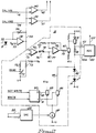
- An optical disk 10 (Fig. 1) is mounted for rotation in an optical disk recorder/player in which an optical system 11, including the usual beam splitters and the like, supplies to the disk 10 a light beam generated by laser 14 through objective lens 12 over light path 13 and receives reflected light from disk 10 over the same path and objective lens 12.
- the light beam is directed through optics 11 to disk 10 as controlled by laser control circuit 15.
- the recorder-player is under control of a programmed microprocessor 20 which has a random access memory (RAM) 21.
- Microprocessor 20 supplies a digital value over cable 22 to digital-to-analog converter (DAC) 23.
- DAC 23 supplies an analog signal to laser control circuit 15 to set the beam intensity emitted by laser 14 to optics 11.
- Such laser output light intensity includes modulation based upon data as supplied by microprocessor 20, or other data handling circuits.
- Line 24 from microprocessor 20 to the laser control circuit 15, provides additional mode control to control the laser control circuit 15.
- Laser 14 is controlled in intensity by a feedback circuit in laser control circuit 15.
- Laser 14 emits an auxiliary beam over light path 30 to a photo diode 31 which also receives reflected light from optic 11.
- Photo diode 31 varies the photo current amplitude in accordance with the light emitted by laser 14 over path 30, including feedback.
- the main beam may be used to illuminate photo diode 31 by passing the beam through appropriate optical components including beam splitters.
- Transimpedance amplifier 32 compares current amplitude through the diode 31 with a reference value on line 33 to supply signals over line 34 indicative of laser output beam intensity.
- Potentiometer 38 adjusts the gain of the transimpedance amplifier 32. This adjustment provides a calibrated signal level on line 34 in volts per watt. As a result, the signal level on line 34 represents the light power output of laser 14.
- Laser control circuit in normal operation, responds to the signal level on line 34 to maintain the laser 14 operation at predetermined intensity values.
- Additional circuits are provided to process the signal on line 34 to enable automatic calibration of DAC 23 so that numerical values on cable 22 accurately represent a desired light intensity output of laser 14.
- DAC 23 is calibrated based upon the intensity of laser 14 at a minimal or safe power level P1 and a maximal or high power level P2.
- a first analog comparator 40 receives the signal on line 34 at one input and at the other input on line 41 a reference value indicative of a first predetermined value CAL VR1 which is a voltage level corresponding to the desired minimal or safe power level, P1. Comparator 40 supplies an inactive signal over line 42 to microprocessor 20 at all times until the signal on line 34 indicates that laser 14 is emitting a light beam equal to or greater than the minimal value. At this time comparator 40 supplies an active signal over line 42 to microprocessor 20. Microprocessor 20 then stores the value input to DAC 23 in table 43 of RAM 21 for later calculation of values to be used in controlling laser 14.
- An analog-to-digital converter (ADC) 100 is connected over line 101 to laser control circuit 15 and over line 102 to microprocessor 20.
- ADC 100 measures the drive current for laser 14, that is, the output current of laser control circuit 15.
- the digitised output of ADC 100 representing the drive current for power level P1 at an out-of-focus condition is also recorded in table 43.
- the microprocessor 20 is programmed continuously to increase the numerical value over cable 22 thereby to cause DAC 23 to actuate laser 14 at ever increasing power levels to increase output light intensities.
- a second analog comparator 35 receives the signal on line 34 at one input and at the other input on line 36 a reference value indicative of a second predetermined value CAL VR2 which is a voltage level corresponding to the maximal or high power level P2. The repetitive step-by-step increase continues until comparator 35 detects a signal on line 34 which is greater in amplitude than the reference signal CAL VR2, on line 36 representing a maximal power level P2, producing a desired reference output light intensity of laser 14. Comparator 35 when sensing the line 34 signal being less than the reference signal on line 36 supplies an inactive signal over line 37 to microprocessor 20.
- microprocessor 20 stores that DAC 23 input value in table 43. At this point, microprocessor 20 also records the digitised output of ADC 100 representing the drive current producing power level P2.
- Comparator 40 receives the signal on line 34 as an indication of laser 14 intensity.
- the DAC 23 setting is increased until the signal on line 34 matches the CAL VR1 signal which produces the first predetermined power level, P1.
- the DAC 23 setting is recorded in table 43 as is the ADC 100 output representing the laser drive current needed to produce power level P1 at the in-focus condition.
- an amplifier 70 receives a signal from line 34.
- a reference input at line 71 controls amplifier 70 during read operations.
- Resistor network 73 is coupled to reference voltages with the bias supplied to amplifier 70 over line 71 being varied by the read switch 72.
- the signal voltage amplitude difference between the signals on line 34 and line 71 is the voltage error output between a desired read laser power level and the actual laser output power level.
- Amplifier 70 amplifies this error voltage and supplies it through control switch 75 as closed for read operations by a signal from microprocessor 20 received over line 76.
- Capacitor 77 smooths the signal received from amplifier 70 and acts as a sample and hold capacitor when switch 75 is open.
- a second amplifier 78 buffers and amplifies the error signal to pass it through resistor 79 to a controlling transistor 80, which acts as a current control for a second transistor 81 which has its base connected to the collector of transistor 80.
- Transistor 81 supplies a drive current from a reference source +V1 which flows through resistor 112, voltage shifting diode 82 and thence to laser diode 14 to cause emission of light. Voltage across resistor 112 on lines 101 and 101A acts to sense the value of the drive current which is then converted by ADC 100 to a representative digital value on line 102.
- the drive current value flowing through transistor 81 is the total value for the mode involved.
- the current from transistor 81 is partially diverted through a transistor 86 to current sink 87.
- the value of current through current sink 87 is controlled by DAC 23, therefore controlling the laser 14 emission.
- a WRITE signal is supplied to switch 90, in the form of a flip-flop.
- a transistor turn-off signal supplied over line 91 makes transistor 86 non-conductive. This action forces the current from transistor 81 to flow through the laser diode 14 to cause maximum emission of radiation or maximum light output.
- the line 92 from the flip-flop 90 switches transistor 93 to current conduction to replace the current in current sink 87 previously supplied by transistor 86.
- the result is recording binary ones on the record medium 10.
- a NOT WRITE signal is supplied to flip-flop 90.
- the current conduction of transistors 86 and 93 is reversed to divert current from transistor 81 to reduce the emission of radiation or light from laser 14.
- switch 75 During reading operations, switch 75 being closed, a laser 14 control loop exists such that the line 34 signal (representing emitted laser light power) matches the line 71 signal (desired read laser output power level).
- DAC 23 Upon each change of input value to DAC 23, a time delay is required to allow the laser control servo loop described above to reach an equilibrium operating point. During this time delay, the change in current flowing through transistor 81 is allowed to stabilise.
- switch 75 is kept open to prevent the above described servo action from changing the laser drive current during recording or erasing.
- Comparators 35 and 40 are used to calibrate the DAC 23.
- voltage CAL VR1 is supplied over line 41 to comparator 40 to detect the lower power laser output.
- voltage CAL VR2 is supplied over line 36 to comparator 35 to detect the higher power laser ouput level.
- curve 190 is produced for an in-focus condition showing the power levels produced at corresponding current levels.
- Curve 191 is produced for a maximum out-of-focus condition showing the power levels produced at corresponding current levels.
- the power level P0 represents that threshold power level at which lasing mode is achieved.
- the corresponding threshold current level is designed ITH ni for the in-focus condition and ITH no for the maximum out-of-focus condition.
- a low reference power level, P1 is chosen so that write-once media will not be altered when the lens is in-focus.
- a high reference power level P2 is chosen such that the difference in laser current to produce P2 is small between in-focus and maximum out-of-focus conditions.
- the characteristic curves 190 and 191 approach asymptotically at high power levels.
- the calibration operation of this invention finds the change in laser DAC value, ⁇ DAC2, that is required to produce a change in laser power from a first low reference power level. P1, to a second high reference power level P2, while the laser beam is out-of-focus. Also, the change in laser DAC value, ⁇ DAC1, is found that is required to change the laser bias current for the low power level P1 with the laser beam in-focus to the power level P1 with the laser beam out-of-focus.
- the power level P1 is a low or safe laser power level for WORM media when the laser beam is in-focus on the media.
- the laser DAC efficiency E is then calculated as the change in laser power (P2 - P1), divided by the sum of the change in DAC value ( ⁇ DAC1 + DAC2).
- step 200 the objective lens is moved away from the media to a maximum out-of-focus condition before the laser is turned on.
- the laser is turned on with the DAC set to zero, laser power control loop (LPCL) closed by closing switch 75 and, with write data set inactive, the laser power level is read as P1.
- the laser drive current I2 (Fig. 3) is then measured with ADC 100 and saved as ADC1. Power level P2 is selected at step 203 and a determination made at step 204 whether P2 has been reached. If not, the DAC value is incremented at step 205 with switch 75 open and write data active.
- the switch 75 is then closed, write data is set inactive and power is again measured. The process is repeated until the DAC value is found that is required to obtain P2 and that DAC value is stored as DAC2 at step 206.
- the laser current I2 (Fig. 3) is again measured with the ADC 100 and saved as ADC2 at step 206.
- the LPCL is closed and the DAC is reset which returns the laser power level to P1, at step 207.
- the laser beam is put into focus on the media at step 208 and the laser bias current I3 (Fig. 3) is measured with the ADC 100 and saved as ADC3 at step 209. At this point, calculations are all that remain of the DAC calibration procedure, and these are performed in the microprocessor 20 at step 210.
- step 210 the change in laser DAC value is found that is required to change the laser drive current from P1 with the laser beam in-focus to P1 with the laser beam out-of-focus as ⁇ DAC1 in Equation (1).
- DAC1 ⁇ DAC2 x (ADC1 - ADC3)/(ADC2 - ADC1)
- the DAC efficiency E1 is calculated as in Equation (2).
- E (P2 - P1)/(DAC2 + ⁇ DAC1)
- the DAC value DACn can be calculated for any laser power level P1p as shown in Equation (3). Also the laser power can be found for any DAC value DACn, as shown in Equation (4).
- the objective lens is moved to a maximum out-of-focus condition and initialising operations are carried out at step 301 to turn the laser on, select power level P0, reset the DAC, and establish read power level P0 with switch 75 closed and write data inactive.
- step 302 it is determined whether the power level has reached P1. If not, the DAC is incremented at step 303 with switch 75 open and write data active. Then switch 75 is closed and write data is set inactive to measure the power level.
- the process repeats until the power level P1 is reached, when at step 304, the laser drive current I1 for producing power level P1 is measured, converted to a digital value by ADC 100 and saved as ADC1 whilst the DAC value is stored as DAC 1. Thereafter the power level P2 is selected at step 305 and a determination made at step 306 whether P2 has been reached. If not, the DAC is incremented at step 307 and power measured again until power level P2 is reached. At step 308, the DAC setting is stored as DAC2, laser drive current I2 is measured and stored as ADC2, and the DAC is then reset. Thus power level P0 is again established. Power level P1 is selected as a search value at step 309, and focus is acquired at step 310.
- ⁇ DAC1 (DAC2-DAC1) ⁇ ((ADC1-ADC3)/(ADC2-ADC1))
- E (P2 - P1)/((DAC2 - DAC1) + ⁇ DAC1))
- DAC settings are saved for each power level P1 and P2 as before, and these numbers are used to represent drive current.
- the lens is moved out-of-focus and the system is initialised at step 401.
- the DAC is incremented until target power level P1 is reached at steps 402 to 404, and the DAC setting DAC1 is saved at step 405.
- power P2 is reached and the DAC setting DAC2 is saved at step 409.
- the DAC is reset and the read power level P0 is established by closing the laser power control loop (LPCL) by closing switch 75.
- the laser DAC transfer function has been calculated and used for checking of the laser power control system.
- the units of the DAC transfer function E are mW/DAC step.
- another transfer function is calculated. This is called the ADC transfer function n, with units of mW/ADC step as the change in ADC value is found that is required to produce a predetermined change in laser power.
- the laser efficiency Gd can be estimated from the DAC transfer function E if the DAC conversion rate K3 in units of mA/DAC step is known.
- Gd E/K3
- the laser efficiency in units of mW/mA can be calculated from both equations (13) and (14) and the results compared to each other and against absolute limits. If the two efficiency calculations are the same but are out of the specified range, a fault is indicated in the laser diode. If the two efficiencies are not equal, a fault is indicated in the laser drive circuit.
- ADC/mA K1 K2
- the laser bias threshold current is measured by measuring the bias current with the ADC before the laser is turned on. This is called an offset value.
- the laser is then turned on at some power level, for example, 0.5 mW, and the laser bias current is then measured with the ADC with the offset value subtracted. If a limit is established on the maximum laser bias current at this power level, ie, 80 mA in this example, and the ADC to laser bias current conversion rate is known to be 1.5 ADC bits per mA, a limit on the measured ADC value can be established, for example, 120 steps. If the ADC value is exceeded, the laser power control system is faulty.
Abstract
Description
- This invention relates to the calibration of optical apparatus.
- Optical disk devices are used for the storage of computer prepared data and have recognised value in their ability to store large quantities of data. The media for use in such devices is reactive to bursts of light such as may be produced by the rapid switching of a semiconductor laser. In order to write data on optical media, the laser power must be controlled at a fairly high power level in order that the media can be altered to reflect the presence or absence of data. In reading the data back, the laser power level is controlled to a lower level so that the media is not altered by the laser beam.
- Optical media is of two general types. That is, media which can be written only once and media which can be written, erased and written again. Write once media (WORM) is permanently altered when "write" power levels are produced by the laser beam while erasable media such as magnetooptic (MO) media is not permanently altered when data is written. In the MO media, the magnetic orientation of the reactive material is altered in the writing process and in the erasing process the magnetic orientation is reordered.
- In operating an optical disk system, it is necessary to set the correct laser power level to read and to write for each optical disk. The correct parameters for the optical disk are included in information in an identification header stamped onto the disk itself. That information, when read by the system, enables a calibration circuit to set the desired current levels for the laser to produce correct laser power. As the laser is subject to unintended changes in its operating parameters particularly with temperature and ageing, the calibration method is also used to change current levels for the laser so that the correct power level is maintained under operating conditions and throughout laser life. The common practice of calibrating the laser circuits to operate with a given optical medium usually involves analysing the laser light intensity at the optical medium. To do that, the laser control circuits are set to match a predetermined or desired light intensity at the optical medium. Analysis is conducted to enable setting digital-to-analog converters (DAC) for controlling laser power in the writing, and the erasing operations of optical mediums. With a WORM media, the high light intensities needed to calibrate the circuit might write on the disk and thereby cause permanent alteration of the media during the calibration process. Therefore, it has become common practice to calibrate WORM media with the laser beam out-of-focus at high power levels in order to calibrate without permanent alteration of the media. It is possible to use out-of-focus conditions as the optical path for WORM media is designed to eliminate light feedback reflected from the optical disk. With MO media, the common practice is to calibrate the system under in focus conditions in order to obtain accurate power levels as optical feedback cannot be eliminated from the optical path. One of the effects of such feedback is a change in the laser power versus bias current (P-I curve), and, therefore, calibration should take place under in-focus conditions.
- For MO media, the power level for the "write" DAC calibration could be performed with the laser beam in-focus. However, with WORM media, the "write" DAC power level cannot be calibrated with the laser beam in focus as permanent alteration of the media would result.
- US-A-4,785,443 describes an optical disk system and laser light control circuit for WORM disk media. The "write" laser power calibration is performed with the media out of focus in order to protect the storage media from permanent alteration.
- The present invention seeks to provide a calibration technique which can be used on both "write once, read many" (WORM) disk media, but also erasable magneto-optic (MO) media.
- This invention provides a calibration technique and apparatus for establishing the correct power levels with which to drive a semiconductor laser at power levels that are safe for write once media in the presence of optical feedback so that either erasable or write-once media can be used. At very high power levels the in-focus and out-of-focus P-I curves approach each other and therefore the difference in current between the in-focus and out-of-focus condition is small. As a result, a high power level is chosen to implement the invention at a level where the difference in current is small. In that manner a calibration technique is presented which enables the user of a high power level to calibrate the laser at an out-of-focus condition regardless of the type of media located in the disk drive.
- In an embodiment of the invention, the objective lens is moved to an out-of-focus condition and a first predetermined low power level is attained; the current level and DAC setting are recorded. Next, the power is increased to a second predetermined high power level where in-focus and out-of-focus P-I curves are asymptotic; the current level and DAC setting are recorded. Next, the power level is dropped to approximately the first predetermined level and the objective lens is moved so that the laser beam is in-focus. The power level is adjusted to the first predetermined power level and the current level and DAC setting are recorded. In that manner, the slope of the in-focus and the slope of the out-of-focus curves are determined. With that information, any particular power level, for example, a "write" power level which might be half way between the high and low calibration levels can be accurately set.
- The scope of the invention is defined by the appended claims; and how the invention may be carried into effect is hereinafter particularly described with reference to the accompanying drawings in which:
- Figure 1 is a block diagram of an optical disk recorder incorporating present invention;
- Figure 2 is a diagram showing the laser control circuit for the recorder of Figure 1;
- Figure 3 is a diagram of the P-I curve for in-focus and out-of-focus conditions;
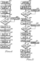
- Figure 4 is a simplified flowchart of a machine operation for calibration in accordance with the invention;
- Figure 5 is a flowchart of generalised machine operation for the calibration according to the invention; and
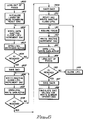
- Figure 6 is a flowchart of an alternative operation for calibration according to the invention.
- An optical disk 10 (Fig. 1) is mounted for rotation in an optical disk recorder/player in which an optical system 11, including the usual beam splitters and the like, supplies to the disk 10 a light beam generated by laser 14 through
objective lens 12 overlight path 13 and receives reflected light from disk 10 over the same path andobjective lens 12. The light beam is directed through optics 11 to disk 10 as controlled bylaser control circuit 15. The recorder-player is under control of a programmedmicroprocessor 20 which has a random access memory (RAM) 21.Microprocessor 20 supplies a digital value overcable 22 to digital-to-analog converter (DAC) 23.DAC 23 supplies an analog signal tolaser control circuit 15 to set the beam intensity emitted by laser 14 to optics 11. Such laser output light intensity includes modulation based upon data as supplied bymicroprocessor 20, or other data handling circuits.Line 24 frommicroprocessor 20 to thelaser control circuit 15, provides additional mode control to control thelaser control circuit 15. - Laser 14 is controlled in intensity by a feedback circuit in
laser control circuit 15. Laser 14 emits an auxiliary beam overlight path 30 to aphoto diode 31 which also receives reflected light from optic 11.Photo diode 31 varies the photo current amplitude in accordance with the light emitted by laser 14 overpath 30, including feedback. If desired, the main beam may be used to illuminatephoto diode 31 by passing the beam through appropriate optical components including beam splitters.Transimpedance amplifier 32 compares current amplitude through thediode 31 with a reference value online 33 to supply signals overline 34 indicative of laser output beam intensity.Potentiometer 38 adjusts the gain of thetransimpedance amplifier 32. This adjustment provides a calibrated signal level online 34 in volts per watt. As a result, the signal level online 34 represents the light power output of laser 14.Laser control circuit 15, in normal operation, responds to the signal level online 34 to maintain the laser 14 operation at predetermined intensity values. - Additional circuits are provided to process the signal on
line 34 to enable automatic calibration ofDAC 23 so that numerical values oncable 22 accurately represent a desired light intensity output of laser 14.DAC 23 is calibrated based upon the intensity of laser 14 at a minimal or safe power level P1 and a maximal or high power level P2. - A first analog comparator 40 receives the signal on
line 34 at one input and at the other input on line 41 a reference value indicative of a first predetermined value CAL VR1 which is a voltage level corresponding to the desired minimal or safe power level, P1. Comparator 40 supplies an inactive signal overline 42 tomicroprocessor 20 at all times until the signal online 34 indicates that laser 14 is emitting a light beam equal to or greater than the minimal value. At this time comparator 40 supplies an active signal overline 42 tomicroprocessor 20.
Microprocessor 20 then stores the value input toDAC 23 in table 43 ofRAM 21 for later calculation of values to be used in controlling laser 14. - An analog-to-digital converter (ADC) 100 is connected over
line 101 tolaser control circuit 15 and overline 102 tomicroprocessor 20.ADC 100 measures the drive current for laser 14, that is, the output current oflaser control circuit 15. When the predetermined power level P1 is, reached and the correspondingDAC 23 setting is recorded in table 43, the digitised output ofADC 100 representing the drive current for power level P1 at an out-of-focus condition is also recorded in table 43. - The
microprocessor 20 is programmed continuously to increase the numerical value overcable 22 thereby to causeDAC 23 to actuate laser 14 at ever increasing power levels to increase output light intensities. Asecond analog comparator 35 receives the signal online 34 at one input and at the other input on line 36 a reference value indicative of a second predetermined value CAL VR2 which is a voltage level corresponding to the maximal or high power level P2. The repetitive step-by-step increase continues untilcomparator 35 detects a signal online 34 which is greater in amplitude than the reference signal CAL VR2, online 36 representing a maximal power level P2, producing a desired reference output light intensity of laser 14.Comparator 35 when sensing theline 34 signal being less than the reference signal online 36 supplies an inactive signal overline 37 tomicroprocessor 20. As soon ascomparator 35 determines that theline 34 signal exceeds the reference signal online 36, then an active signal is supplied overline 37 tomicroprocessor 20, whereuponmicroprocessor 20 stores thatDAC 23 input value in table 43. At this point,microprocessor 20 also records the digitised output ofADC 100 representing the drive current producing power level P2. - After dropping the power level back to a level somewhat below level P1, the
objective lens 12 is moved to bring the laser beam into focus at the surface of optical disk 10. Comparator 40 receives the signal online 34 as an indication of laser 14 intensity. TheDAC 23 setting is increased until the signal online 34 matches the CAL VR1 signal which produces the first predetermined power level, P1. At this point, theDAC 23 setting is recorded in table 43 as is theADC 100 output representing the laser drive current needed to produce power level P1 at the in-focus condition. - In laser control circuit 15 (Fig. 2), an amplifier 70 receives a signal from
line 34. A reference input at line 71 controls amplifier 70 during read operations.Resistor network 73 is coupled to reference voltages with the bias supplied to amplifier 70 over line 71 being varied by theread switch 72. The signal voltage amplitude difference between the signals online 34 and line 71 is the voltage error output between a desired read laser power level and the actual laser output power level. Amplifier 70 amplifies this error voltage and supplies it through control switch 75 as closed for read operations by a signal frommicroprocessor 20 received over line 76. Capacitor 77 smooths the signal received from amplifier 70 and acts as a sample and hold capacitor when switch 75 is open. Asecond amplifier 78 buffers and amplifies the error signal to pass it throughresistor 79 to a controlling transistor 80, which acts as a current control for asecond transistor 81 which has its base connected to the collector of transistor 80.Transistor 81 supplies a drive current from a reference source +V1 which flows throughresistor 112,voltage shifting diode 82 and thence to laser diode 14 to cause emission of light. Voltage acrossresistor 112 onlines 101 and 101A acts to sense the value of the drive current which is then converted byADC 100 to a representative digital value online 102. The drive current value flowing throughtransistor 81 is the total value for the mode involved. For recording, this means a recording level of current flowing through laser diode 14 to actuate it to emit an output light having a power level for recording on a record medium. Between the writing impulses i.e., the record zeros or no change in the record medium, the current fromtransistor 81 is partially diverted through atransistor 86 tocurrent sink 87. The value of current throughcurrent sink 87 is controlled byDAC 23, therefore controlling the laser 14 emission. A WRITE signal is supplied to switch 90, in the form of a flip-flop. A transistor turn-off signal supplied overline 91 makestransistor 86 non-conductive. This action forces the current fromtransistor 81 to flow through the laser diode 14 to cause maximum emission of radiation or maximum light output. Simultaneously, theline 92 from the flip-flop 90switches transistor 93 to current conduction to replace the current incurrent sink 87 previously supplied bytransistor 86. The result is recording binary ones on the record medium 10. When a NOT WRITE signal is supplied to flip-flop 90. the current conduction oftransistors transistor 81 to reduce the emission of radiation or light from laser 14. - During reading operations, switch 75 being closed, a laser 14 control loop exists such that the
line 34 signal (representing emitted laser light power) matches the line 71 signal (desired read laser output power level). Eachtime microprocessor 20 changes theDAC 23 input value, it closes switch 75 and sets flip-flop 90. Thentransistor 86 becomes current conductive. This action changes the current amplitude incurrent sink 87 so that the amount of current being diverted fromtransistor 81 is also changed. Upon each change of input value toDAC 23, a time delay is required to allow the laser control servo loop described above to reach an equilibrium operating point. During this time delay, the change in current flowing throughtransistor 81 is allowed to stabilise. During recording or erasing modes, switch 75 is kept open to prevent the above described servo action from changing the laser drive current during recording or erasing. -
Comparators 35 and 40 are used to calibrate theDAC 23. During the calibration phase at the predetermined low power level P1, voltage CAL VR1 is supplied overline 41 to comparator 40 to detect the lower power laser output. During calibration at the predetermined high power level P2, voltage CAL VR2 is supplied overline 36 tocomparator 35 to detect the higher power laser ouput level. - In two power-current characteristic curves (Fig. 3) for a semiconductor laser,
curve 190 is produced for an in-focus condition showing the power levels produced at corresponding current levels. Curve 191 is produced for a maximum out-of-focus condition showing the power levels produced at corresponding current levels. The power level P0 represents that threshold power level at which lasing mode is achieved. The corresponding threshold current level is designed ITH ni for the in-focus condition and ITH no for the maximum out-of-focus condition. A low reference power level, P1, is chosen so that write-once media will not be altered when the lens is in-focus. A high reference power level P2 is chosen such that the difference in laser current to produce P2 is small between in-focus and maximum out-of-focus conditions. Thecharacteristic curves 190 and 191 approach asymptotically at high power levels. - At high laser power, the difference in laser power, for a given laser bias current, is small whether the laser beam is in or out-of-focus. The calibration operation of this invention finds the change in laser DAC value, Δ DAC2, that is required to produce a change in laser power from a first low reference power level. P1, to a second high reference power level P2, while the laser beam is out-of-focus. Also, the change in laser DAC value, Δ DAC1, is found that is required to change the laser bias current for the low power level P1 with the laser beam in-focus to the power level P1 with the laser beam out-of-focus. The power level P1 is a low or safe laser power level for WORM media when the laser beam is in-focus on the media. The laser DAC efficiency E is then calculated as the change in laser power (P2 - P1), divided by the sum of the change in DAC value (Δ DAC1 + DAC2).
- In machine operation (Fig. 4) where it is assumed that P1 = P0, and that DAC1 = 0 at P0, at
step 200 the objective lens is moved away from the media to a maximum out-of-focus condition before the laser is turned on. Instep 201, the laser is turned on with the DAC set to zero, laser power control loop (LPCL) closed by closing switch 75 and, with write data set inactive, the laser power level is read as P1. Instep 202, the laser drive current I2 (Fig. 3) is then measured withADC 100 and saved as ADC1. Power level P2 is selected atstep 203 and a determination made atstep 204 whether P2 has been reached. If not, the DAC value is incremented atstep 205 with switch 75 open and write data active. The switch 75 is then closed, write data is set inactive and power is again measured. The process is repeated until the DAC value is found that is required to obtain P2 and that DAC value is stored as DAC2 atstep 206. The laser current I2 (Fig. 3) is again measured with theADC 100 and saved as ADC2 atstep 206. Then the LPCL is closed and the DAC is reset which returns the laser power level to P1, at step 207. Thereafter, the laser beam is put into focus on the media atstep 208 and the laser bias current I3 (Fig. 3) is measured with theADC 100 and saved as ADC3 atstep 209. At this point, calculations are all that remain of the DAC calibration procedure, and these are performed in themicroprocessor 20 atstep 210. - In
step 210 calculations, the change in laser DAC value is found that is required to change the laser drive current from P1 with the laser beam in-focus to P1 with the laser beam out-of-focus as ΔDAC1 in Equation (1).
The DAC efficiency E1 is calculated as in Equation (2).
- The DAC value DACn, can be calculated for any laser power level P1p as shown in Equation (3). Also the laser power can be found for any DAC value DACn, as shown in Equation (4).


- In the calibration method (Fig. 5) which does not assume P1 = P0 and where the DAC setting is not necessarily equal to zero at P1, at
step 300, the objective lens is moved to a maximum out-of-focus condition and initialising operations are carried out atstep 301 to turn the laser on, select power level P0, reset the DAC, and establish read power level P0 with switch 75 closed and write data inactive. Atstep 302, it is determined whether the power level has reached P1. If not, the DAC is incremented atstep 303 with switch 75 open and write data active. Then switch 75 is closed and write data is set inactive to measure the power level. The process repeats until the power level P1 is reached, when atstep 304, the laser drive current I1 for producing power level P1 is measured, converted to a digital value byADC 100 and saved as ADC1 whilst the DAC value is stored as DAC 1. Thereafter the power level P2 is selected atstep 305 and a determination made atstep 306 whether P2 has been reached. If not, the DAC is incremented atstep 307 and power measured again until power level P2 is reached. Atstep 308, the DAC setting is stored as DAC2, laser drive current I2 is measured and stored as ADC2, and the DAC is then reset. Thus power level P0 is again established. Power level P1 is selected as a search value atstep 309, and focus is acquired atstep 310. A determination is made atstep 311 whether P1 has been reached. If not, the DAC in incremented atstep 312 until power level P1 is reached. At step 313, the DAC setting is stored as DAC3 and the drive current I3 is measured and stored as ADC3. Atstep 314 the microprocessor performs calculations according to Equations (5) to (8).


- An alternative method (Fig. 6) of calibrating the laser does not require the use of an ADC and makes use of the linear nature of the laser P-I characteristic curve (Fig. 3). DAC settings are saved for each power level P1 and P2 as before, and these numbers are used to represent drive current. At
step 400, the lens is moved out-of-focus and the system is initialised atstep 401. The DAC is incremented until target power level P1 is reached atsteps 402 to 404, and the DAC setting DAC1 is saved atstep 405. Atsteps 406 to 408, power P2 is reached and the DAC setting DAC2 is saved atstep 409. Atstep 410, the DAC is reset and the read power level P0 is established by closing the laser power control loop (LPCL) by closing switch 75. Focus is acquired atstep 411. Next, atsteps 412 to 417, the DAC3 value is found and saved. Atstep 418, the efficiency E is calculated using Equation (9)
where ΔDAC1 = DAC2 - DAC1 and ΔDAC2 = DAC3 - DAC1. - In using this invention, it will not be known whether MO or WORM media is inserted into the drive until after the control tracks are read. Therefore, the erase/write DAC calibration should be performed with the laser beam out-of-focus. If MO media is in the drive, the DAC calibration results are still valid.
- With the above invention, additional checking of the laser drive circuit can be performed.
- In prior art, the laser DAC transfer function has been calculated and used for checking of the laser power control system. The units of the DAC transfer function E, are mW/DAC step. In the system described herein, by monitoring the laser bias current with the ADC, another transfer function is calculated. This is called the ADC transfer function n, with units of mW/ADC step as the change in ADC value is found that is required to produce a predetermined change in laser power. The equations to calculate the ADC transfer function are shown below for both out-of-focus (no) and in-focus (ni) conditions.


- The transfer functions no and ni can be rewritten as the laser efficiency Ga in units of mW/mA, divided by the current-to-voltage converter gain K1 in units of V/mA, and the
ADC 100 conversion factor K2 in units of ADC steps. This is shown below inequation 12.
- From the circuit implementation, if the current-to-voltage converter gain K1, and ADC conversion factor K2 are known, the laser efficiency Ga can be calculated in units of mW/mA as follows.

- In a like manner, the laser efficiency Gd can be estimated from the DAC transfer function E if the DAC conversion rate K3 in units of mA/DAC step is known.

- From the DAC calibration, as both the DAC transfer function E, and ADC transfer function n, are found, the laser efficiency in units of mW/mA can be calculated from both equations (13) and (14) and the results compared to each other and against absolute limits. If the two efficiency calculations are the same but are out of the specified range, a fault is indicated in the laser diode. If the two efficiencies are not equal, a fault is indicated in the laser drive circuit.
- In addition, by comparing the results of the two efficiency calculations against each other, many other circuit functions in the laser driver and the current sensing elements can be checked, such as the current-to-voltage converter gain K1, the ADC conversion factor K2, and the DAC conversion rate K3. Assuming that the two laser efficiencies, Ga and Gd are equal, the relationship between the ADC transfer function, n, and the laser DAC transfer function E is shown in equation (15). The DAC/ADC rate, DAC steps per ADC steps is the reciprocal of the product of the DAC conversion rate K3 (mA/DAC), the current-to-voltage rate K1 (V/mA), and the ADC conversion rate K2. These K factor quantities are controlled by the circuit design and should remain stable over time, thus limits can be established on the DAC to ADC conversion (DAC/ADC) rate. By placing limits on the DAC/ADC, the function of several circuit elements can be checked.

- The relationship between ADC values and the laser bias current (ADC/mA) is established as shown in equation (16). These quantities are a subset of
equation 15, thus also remain stable over time. Reasonable limits are established on the ADC to laser bias current (ADC/mA) conversion rate to check the ADC and laser functions.
- By monitoring the laser bias current with the ADC, additional checking can be performed on the laser power control system. When a command is given to change the laser DAC it can be verified that the DAC did change because the relationship is known from Equation (15). Also a check can be made on the laser threshold current (or the laser bias current at some power level), when the laser is turned on or when a potential fault is present because the relationship between ADC value and laser bias current (ADC/mA) is known from Equation (16).
- The laser bias threshold current is measured by measuring the bias current with the ADC before the laser is turned on. This is called an offset value. The laser is then turned on at some power level, for example, 0.5 mW, and the laser bias current is then measured with the ADC with the offset value subtracted. If a limit is established on the maximum laser bias current at this power level, ie, 80 mA in this example, and the ADC to laser bias current conversion rate is known to be 1.5 ADC bits per mA, a limit on the measured ADC value can be established, for example, 120 steps. If the ADC value is exceeded, the laser power control system is faulty.
- Several other possibilities exist with the ability to measure the laser bias current with an ADC. Some of these are as follows. By sampling the laser bias current with the ADC before the process of bringing the object lens in-focus with the media, it can be verified that focus has been acquired as the laser bias current will decrease because of light being fed back into the laser cavity. Also during the focus acquire process, by monitoring the bias current with the ADC, it can be detected when the objective lens is coming into focus. This is an alternative method to detecting the Focus Error Signal (FES) peak. Also by monitoring the laser bias current with the ADC while adjusting the FES offset, the point of minimum laser bias current will suggest optimum focus as the laser feedback will be a maximum.
- While the invention has been particularly shown and described with reference to preferred embodiments thereof, it will be understood by those skilled in the art that various changes in form and details may be made therein without departing from the scope of the invention:
Claims (18)
- A method for calibrating apparatus employing semi-conductor laser diodes subject to reflective optical feedback from a target surface wherein the power output vs. drive current characteristic curves for the laser diode exhibit an asymptotic region for in-focus and out-of-focus conditions at high power levels, including establishing an out-of-focus condition on the target surface, energising the laser diode to produce a predetermined first low laser power level (P1) and measuring the laser drive current (I1) needed to produce the low power level at the out-of-focus condition, energising the laser diode to produce a predetermined high laser power level (P2) selected within the asymptotic region, and measuring the laser drive current (I2) needed to produce the high level, energising the laser diode to produce the first low power level P1, establishing an in-focus condition on the target surface, and measuring the laser drive current (I3) needed to produce the first low power level (P1) at the in-focus condition.
- A method according to claim 1, including determining the slope of the power vs. current characteristic curve for in-focus conditions using the relationship (P2 - P1)/(I2 - I3).
- A method according to claim 1 or 2, including determining the slope of the power vs. current characteristic curve for out-of-focus conditions using the relationship (P2 - P1)/(I2 - I1).
- A method according to claim 1, 2 or 3, wherein the apparatus includes a digital-to-analog converter (DAC) for setting drive current levels, the method including saving the DAC setting (DAC1) to produce the predetermined low power level (P1), energising the laser diode saving the DAC setting (DAC2) to produce the predetermined high power level (P2), and saving the DAC setting (DAC3) to produce the predetermined low power level (P1) for the in-focus condition.
- A method according to claim 4, including determining the change in DAC value (ΔDAC1) to change laser drive current from in-focus power level (P1) to out-of-focus power level (P1) using the relationship


- A method according to claim 4 or 5, wherein the apparatus includes an analog-to digital converter (ADC) for measuring drive current levels, the method including saving the ADC setting (ADC1) at the predetermined low level power level P1 for the out-of-focus condition, saving the ADC setting (ADC3) at the predetermined power level P1 for the in-focus condition.
- A method according to claim 6, including determining the change in DAC value (ΔDAC1) required to change laser drive current from in-focus low power level (P1) to out-of-focus power level (P1) using the relationship


- A method according to claim 6, wherein the apparatus is adjusted so that low power level (P1) is equal to a threshold power level (P0) at which lasing mode is achieved, and where the DAC is adjusted to a setting of zero at the low power level (P1), including determining the changes in DAC value (ΔDAC1) required to change laser drive current from in-focus low power level (P1) to out-of-focus low power level (P1) using the relationship


- A method according to claim 6, 7 or 8, including the determination of the proper operation of a laser diode and its drive circuitry, the method including obtaining the DAC transfer function (E), the increase in laser power output per DAC step, obtaining the ADC transfer function (n), the increase in laser power output per ADC step, and comparing E and n, and if equal and within a preset range of laser efficiency, indicating no fault, or, if equal by outside the present range of laser efficiency, indicating a first fault, indicative of a faulty laser diode, or, if not equal, indicating a second fault, indicative of a faulty laser driver.
- A method according to claim 9, including comparing the ADC transfer function (n)to the DAC transfer function (E) against a preset range of ADC/DAC ratios, and indicating faulty circuitry if the results of the comparison fall outside the preset range of ratios.
- A method of determining the proper operation of a laser diode and its drive circuitry, wherein laser drive circuitry includes a digital-to-analog converter (DAC) for setting drive current levels an analog-to-digital converter (ADC) for measuring drive current levels, the method including obtaining the DAC transfer function (E), the increase in laser power output per DAC step, obtaining the ADC transfer function (n), the increase in laser power output per ADC step, and comparing E and n, and if equal and within a preset range of laser efficiency, indicating no fault.
- A method according to claim 11, wherein, if the result of the comparison of E and n is equal but outside a preset range of laser efficiency, a first fault, indicative of a faulty laser diode, is indicated.
- A method according to claim 11 or 12, including, if comparison of E and n is not equal, indicating a second fault, indicative of a faulty laser driver.
- A method according to claim 11, 12 or 13, including comparing the ADC transfer function to the DAC transfer function against a preset range of ADC/DAC ratios, and indicating faulty circuitry if the results of the comparison fall outside the preset range of ratios.
- Optical disk apparatus wherein a semiconductor laser diode (14) emits radiation which is directed through a lens (12) to the surface of an optical disk (10) and wherein the laser receives an optical feedback radiation reflected from the surface, the apparatus including means for calibrating the drive current of the laser diode, characterised in that the apparatus comprises
a laser diode (14) and an associated lens (12) for receiving radiation therefrom, actuating means connected to the lens for moving the lens to an in-focus condition from an out-of-focus condition for directing radiation produced by the diode to a target surface, laser drive current means connected to the laser diode, laser drive current control means (15) connected to the drive current means for energising the diode to selected power levels, means for measuring laser drive current levels wherein I1 is the drive current for producing a low power level (P1) at an out-of-focus condition, I3 is the drive current for producing low power level P1 at an in-focus condition and I2 is the drive current for producing high level power P2, and microprocessor means (20) for calculating the slope of the power vs. current characteristic curve for in-focus condition using the relationship (P2 - P1) / (I2 - I3). - An apparatus according to claim 15, wherein the laser drive current control means includes a digital-to-analog converter (DAC) means for establishing DAC value settings DAC1, DAC2, and DAC3, where DAC1 is the setting for producing a low power level P1 at out-of-focus condition, DAC3 is the setting for producing a low power level P1 at in-focus condition, and where DAC2 is the setting for producing a high power level P2 at an out-of-focus condition,
the means for measuring laser drive current levels includes an analog-to-digital converter (ADC) connected to the laser drive control means and to the microprocessor, where ADC1, ADC2 and ADC3 are corresponding digital values for measured current levels I1, I2 and I3,
the microprocessor means determining the change in DAC value (Δ DAC1) required to change laser drive current from in-focus low power level P1 to out-of-focus power level P1 using the relationship:


- Optical disk apparatus wherein a semiconductor laser diode (14) emits radiation which is directed through a lens (12) to the surface of an optical disk (10) and wherein the laser receives an optical feedback radiation reflected from the surface, the apparatus including means for calibrating the drive current of the laser diode, characterised by a laser diode (14) and an associated lens (12) to receive radiation therefrom, actuating means connected to the lens for moving the lens to an in-focus condition from an out-of-focus condition laser drive current means connected to the laser diode, laser drive current control means connected to the laser drive current means for energising the diode to selected power levels, the control means including a digital-to-analog convertor (DAC) for establishing DAC value settings DAC1, DAC2, and DAC3, where DAC1 is the setting for producing a low power level P1 at an out-of-focus condition, DAC3 is the setting for producing the low power level P1 at an in-focus condition, and DAC2 is the setting for producing a high power level P2 at an out-of-focus conditions, and microprocessor means (20) for determining the change in DAC value (ΔDAC1) required to change laser drive current from in-focus power level (P1) to out-of-focus power level (P) using the relationship


- Apparatus according to claim 15, 16 or 17, including means for measuring the output power of the laser diode to establish the selected power levels.
Applications Claiming Priority (2)
| Application Number | Priority Date | Filing Date | Title |
|---|---|---|---|
| US757748 | 1991-09-11 | ||
| US07/757,748 US5216659A (en) | 1991-09-11 | 1991-09-11 | Laser power calibration by measuring laser drive current at out of focus and in focus conditions |
Publications (3)
| Publication Number | Publication Date |
|---|---|
| EP0532241A2 true EP0532241A2 (en) | 1993-03-17 |
| EP0532241A3 EP0532241A3 (en) | 1994-04-06 |
| EP0532241B1 EP0532241B1 (en) | 1997-07-23 |
Family
ID=25049063
Family Applications (1)
| Application Number | Title | Priority Date | Filing Date |
|---|---|---|---|
| EP92308043A Expired - Lifetime EP0532241B1 (en) | 1991-09-11 | 1992-09-04 | Calibration method and apparatus |
Country Status (4)
| Country | Link |
|---|---|
| US (1) | US5216659A (en) |
| EP (1) | EP0532241B1 (en) |
| JP (1) | JP2553284B2 (en) |
| DE (1) | DE69221049T2 (en) |
Cited By (5)
| Publication number | Priority date | Publication date | Assignee | Title |
|---|---|---|---|---|
| EP0793222A2 (en) * | 1996-02-28 | 1997-09-03 | Hamamatsu Photonics K.K. | Optical apparatus |
| EP0803866A3 (en) * | 1996-04-26 | 1998-01-21 | Fujitsu Limited | Optical storage apparatus |
| EP0916441A1 (en) * | 1997-11-14 | 1999-05-19 | Fujifilm Electronic Imaging Limited | Focus detection system and method |
| US6661759B1 (en) | 1999-06-18 | 2003-12-09 | Samsung Electronics Co., Ltd. | Adaptive recording method and apparatus for high-density optical recording, and control method therefor |
| EP1376557A1 (en) * | 2002-06-26 | 2004-01-02 | Hitachi-LG Data Storage Korea Inc. | Method for controlling an optical power level |
Families Citing this family (29)
| Publication number | Priority date | Publication date | Assignee | Title |
|---|---|---|---|---|
| JPH05234082A (en) * | 1992-02-21 | 1993-09-10 | Pioneer Electron Corp | Optical disk player |
| EP0559391B1 (en) * | 1992-03-03 | 1998-06-03 | Canon Kabushiki Kaisha | Magnetooptical recording/reproducing method and apparatus |
| US5383175A (en) * | 1992-12-17 | 1995-01-17 | International Business Machines Corporation | Laser power control with defocusing offset during data recording |
| US5450383A (en) | 1994-05-26 | 1995-09-12 | International Business Machines Corporation | Monitoring and adjusting laser write power in an optical disk recorder using pulse-width modulated power level checking signals |
| US5602814A (en) * | 1994-10-06 | 1997-02-11 | International Business Machines Corporation | Calibration of write-once disks using a single disk sector |
| JP3528612B2 (en) | 1998-02-02 | 2004-05-17 | 株式会社日立製作所 | Optical disk drive |
| JP3718759B2 (en) * | 1999-01-25 | 2005-11-24 | 株式会社日立製作所 | LASER DRIVE DEVICE AND OPTICAL DISC RECORDING / REPRODUCING DEVICE |
| KR100350983B1 (en) * | 2000-02-03 | 2002-08-28 | 삼성전자 주식회사 | Laser diode driver, initializing method of optical recording/reproducing apparatus therefor, and driving method of laser diode driver |
| US6515693B1 (en) | 2000-06-29 | 2003-02-04 | Eastman Kodak Company | Calibration station for a printhead adapted to compensate for the wavelength sensitivity of an image recording material |
| US7522480B2 (en) | 2001-01-25 | 2009-04-21 | Dphi Acquisitions, Inc. | Digital tracking servo system with multi-track seek with an acceleration clamp |
| US7782721B2 (en) * | 2001-01-25 | 2010-08-24 | Dphi Acquisitions, Inc. | Digital focus and tracking servo system with multi-zone calibration |
| US6834065B2 (en) * | 2002-05-21 | 2004-12-21 | Carrier Access Corporation | Methods and apparatuses for direct digital drive of a laser in a passive optical network |
| US7317674B2 (en) * | 2003-03-11 | 2008-01-08 | Intersil Americas Inc. | Optical pick-up units and laser drivers with increased functionality |
| CN1310229C (en) * | 2003-11-17 | 2007-04-11 | 威盛电子股份有限公司 | Method and device for adjusting a control parameter of a servo of an optical drive |
| TWI261226B (en) * | 2004-01-20 | 2006-09-01 | Via Tech Inc | Apparatus and method of dynamic adjusting the detection window |
| TWI261240B (en) | 2004-08-17 | 2006-09-01 | Via Tech Inc | Method for determining data storage quality of optical disc |
| KR100629493B1 (en) * | 2004-10-14 | 2006-09-28 | 삼성전자주식회사 | Optical disk recoding and reproducing apparatus |
| US7515165B2 (en) * | 2004-10-29 | 2009-04-07 | Hewlett-Packard Development Company, L.P. | Laser power calibration in an optical disc drive |
| US7420580B2 (en) * | 2004-10-29 | 2008-09-02 | Hewlett-Packard Development Company, L.P. | Laser power calibration in an optical disc drive |
| US7576765B2 (en) * | 2005-05-11 | 2009-08-18 | Hewlett-Packard Development Company, L.P. | Methods and apparatus for detecting and optimizing laser mark quality on recording media |
| US20060256688A1 (en) * | 2005-05-11 | 2006-11-16 | Van Brocklin Andrew L | Methods and apparatus for shaping mark recorded on media with electromagnetic radiation beam |
| KR100653493B1 (en) * | 2005-05-26 | 2006-12-05 | 주식회사 히타치엘지 데이터 스토리지 코리아 | Method for setting laser power in optical disc driver |
| JP4470815B2 (en) * | 2005-05-31 | 2010-06-02 | 船井電機株式会社 | Output voltage adjustment method for laser power monitor |
| US7729216B2 (en) * | 2005-07-05 | 2010-06-01 | Hewlett-Packard Development Company, L.P. | Methods and apparatus for marking media with collimated electromagnetic radiation beam |
| US7516897B1 (en) * | 2005-09-07 | 2009-04-14 | Kinana Hussain | Digital automatic power control loop for continuous and burst mode applications |
| US7808872B2 (en) * | 2006-07-06 | 2010-10-05 | Intersil Americas Inc. | Hybrid laser diode drivers that include a state machine |
| US8018809B2 (en) | 2007-05-16 | 2011-09-13 | Intersil Americas Inc. | Hybrid laser diode drivers |
| TW201027522A (en) * | 2009-01-09 | 2010-07-16 | Sunplus Technology Co Ltd | Methods for on-line calibrating output power of optical pick-up |
| DE102010052368A1 (en) * | 2010-09-06 | 2012-03-08 | Mtu Aero Engines Gmbh | Method for controlling and / or regulating a laser device and a laser device |
Citations (5)
| Publication number | Priority date | Publication date | Assignee | Title |
|---|---|---|---|---|
| US4747091A (en) * | 1985-07-25 | 1988-05-24 | Olympus Optical Co., Ltd. | Semiconductor laser drive device |
| US4785443A (en) * | 1985-11-14 | 1988-11-15 | Fujitsu Limited | Light control circuit of optical disc system |
| EP0352125A2 (en) * | 1988-07-22 | 1990-01-24 | Sharp Kabushiki Kaisha | A semiconductor laser driving apparatus |
| US5018155A (en) * | 1989-09-22 | 1991-05-21 | Olympus Optical Co., Ltd. | Semiconductor laser driving apparatus to be used for optical information recording and reproducing apparatus |
| EP0467616A2 (en) * | 1990-07-20 | 1992-01-22 | International Business Machines Corporation | control system for light emitting device |
Family Cites Families (11)
| Publication number | Priority date | Publication date | Assignee | Title |
|---|---|---|---|---|
| DE3546645C2 (en) * | 1984-11-20 | 1991-10-17 | Olympus Optical Co., Ltd., Tokio/Tokyo, Jp | |
| US4949329A (en) * | 1985-05-21 | 1990-08-14 | Hoechst Celanese Corp. | Method of effecting erasure of optical information media including varying duty cycle, laser power and focus offset |
| US4937799A (en) * | 1985-12-13 | 1990-06-26 | Canon Kabushiki Kaisha | Method and apparatus for setting light quantity most suitable for reproducing information from an optical recording medium |
| JPS63153455A (en) * | 1986-12-18 | 1988-06-25 | Yokogawa Electric Corp | Optical disk testing system |
| JPS63225925A (en) * | 1987-03-16 | 1988-09-20 | Olympus Optical Co Ltd | Method for recording data on optical card |
| JPH07118166B2 (en) * | 1987-05-21 | 1995-12-18 | パイオニア株式会社 | Tracking circuit |
| US4907212A (en) * | 1988-06-09 | 1990-03-06 | Laser Magnetic Storage International Company | Method and apparatus for calibrating an optical disk system |
| US5070495A (en) * | 1989-04-12 | 1991-12-03 | International Business Machines Corporation | Write calibration for magnetooptic disk recorders |
| US4937440A (en) * | 1989-08-29 | 1990-06-26 | Hewlett-Packard Company | System and method for beam farfield shift focus compensation |
| US5050156A (en) * | 1989-10-25 | 1991-09-17 | Eastman Kodak Company | Method and apparatus for calibrating the writing power applied to an optical media |
| US5136569A (en) * | 1990-09-28 | 1992-08-04 | International Business Machines Corporation | Optical disk recorder for diverse media types and having a predetermined initialization or start-up procedure |
-
1991
- 1991-09-11 US US07/757,748 patent/US5216659A/en not_active Expired - Fee Related
-
1992
- 1992-07-06 JP JP4178142A patent/JP2553284B2/en not_active Expired - Lifetime
- 1992-09-04 DE DE69221049T patent/DE69221049T2/en not_active Expired - Fee Related
- 1992-09-04 EP EP92308043A patent/EP0532241B1/en not_active Expired - Lifetime
Patent Citations (5)
| Publication number | Priority date | Publication date | Assignee | Title |
|---|---|---|---|---|
| US4747091A (en) * | 1985-07-25 | 1988-05-24 | Olympus Optical Co., Ltd. | Semiconductor laser drive device |
| US4785443A (en) * | 1985-11-14 | 1988-11-15 | Fujitsu Limited | Light control circuit of optical disc system |
| EP0352125A2 (en) * | 1988-07-22 | 1990-01-24 | Sharp Kabushiki Kaisha | A semiconductor laser driving apparatus |
| US5018155A (en) * | 1989-09-22 | 1991-05-21 | Olympus Optical Co., Ltd. | Semiconductor laser driving apparatus to be used for optical information recording and reproducing apparatus |
| EP0467616A2 (en) * | 1990-07-20 | 1992-01-22 | International Business Machines Corporation | control system for light emitting device |
Cited By (9)
| Publication number | Priority date | Publication date | Assignee | Title |
|---|---|---|---|---|
| EP0793222A2 (en) * | 1996-02-28 | 1997-09-03 | Hamamatsu Photonics K.K. | Optical apparatus |
| EP0793222A3 (en) * | 1996-02-28 | 1998-04-08 | Hamamatsu Photonics K.K. | Optical apparatus |
| EP0803866A3 (en) * | 1996-04-26 | 1998-01-21 | Fujitsu Limited | Optical storage apparatus |
| US5732055A (en) * | 1996-04-26 | 1998-03-24 | Fujitsu Limited | Optical storage apparatus |
| US6115338A (en) * | 1996-04-26 | 2000-09-05 | Fujitsu Limited | Optical storage apparatus |
| EP0916441A1 (en) * | 1997-11-14 | 1999-05-19 | Fujifilm Electronic Imaging Limited | Focus detection system and method |
| US6661759B1 (en) | 1999-06-18 | 2003-12-09 | Samsung Electronics Co., Ltd. | Adaptive recording method and apparatus for high-density optical recording, and control method therefor |
| EP1376557A1 (en) * | 2002-06-26 | 2004-01-02 | Hitachi-LG Data Storage Korea Inc. | Method for controlling an optical power level |
| US7414934B2 (en) | 2002-06-26 | 2008-08-19 | Hitachi-Lg Data Storage Korea, Inc. | Method for controlling optical power level |
Also Published As
| Publication number | Publication date |
|---|---|
| JPH05189767A (en) | 1993-07-30 |
| EP0532241A3 (en) | 1994-04-06 |
| DE69221049T2 (en) | 1998-01-15 |
| JP2553284B2 (en) | 1996-11-13 |
| EP0532241B1 (en) | 1997-07-23 |
| US5216659A (en) | 1993-06-01 |
| DE69221049D1 (en) | 1997-09-04 |
Similar Documents
| Publication | Publication Date | Title |
|---|---|---|
| EP0532241B1 (en) | Calibration method and apparatus | |
| US5185734A (en) | Calibrating and power-protecting laser drive circuits | |
| US5436880A (en) | Laser power control in an optical recording system using partial correction of reflected signal error | |
| US7095764B2 (en) | Laser driving method and laser driving device | |
| USRE42451E1 (en) | Method and device for generating a stable power control signal | |
| US7009923B2 (en) | Method of and apparatus for recording information | |
| US5640381A (en) | Laser power-drive circuit having a scaling DAC supplying a scaled reference signal to a plurality of scaled DAC's that supply a plurality of scaled output signals | |
| US5172365A (en) | System for predicting laser end-of life from the power vs. current curve of the diode | |
| US5008888A (en) | Semiconductor laser driving apparatus | |
| US7248551B2 (en) | Apparatus and method for controlling laser power for disc drive | |
| US6787748B2 (en) | High speed sampling circuit | |
| US5383175A (en) | Laser power control with defocusing offset during data recording | |
| US20040062164A1 (en) | Optical storage apparatus and abnormality detection method of detector for emission control | |
| US7808871B2 (en) | Power control apparatus and method for an optical drive | |
| EP1098305B1 (en) | Optical disk recording/reproducing device employing waveform correction of laser output signal | |
| EP1213713B1 (en) | Light intensity control and information recording apparatus and method and computer program product | |
| US6754156B2 (en) | Recording apparatus for use with optical recording medium and method thereof | |
| KR100200819B1 (en) | Laser diode power control method and circuit of the optical disk system | |
| JPH08235629A (en) | Control device of semiconductor laser | |
| JP2002367175A (en) | Recording light quantity controller for optical disk | |
| US20020150007A1 (en) | Apparatus for writing an optical record carrier | |
| JPH03245327A (en) | Light emission power control circuit for semiconductor laser |
Legal Events
| Date | Code | Title | Description |
|---|---|---|---|
| PUAI | Public reference made under article 153(3) epc to a published international application that has entered the european phase |
Free format text: ORIGINAL CODE: 0009012 |
|
| AK | Designated contracting states |
Kind code of ref document: A2 Designated state(s): DE FR GB |
|
| 17P | Request for examination filed |
Effective date: 19930716 |
|
| PUAL | Search report despatched |
Free format text: ORIGINAL CODE: 0009013 |
|
| AK | Designated contracting states |
Kind code of ref document: A3 Designated state(s): DE FR GB |
|
| 17Q | First examination report despatched |
Effective date: 19951122 |
|
| GRAG | Despatch of communication of intention to grant |
Free format text: ORIGINAL CODE: EPIDOS AGRA |
|
| GRAH | Despatch of communication of intention to grant a patent |
Free format text: ORIGINAL CODE: EPIDOS IGRA |
|
| GRAH | Despatch of communication of intention to grant a patent |
Free format text: ORIGINAL CODE: EPIDOS IGRA |
|
| GRAA | (expected) grant |
Free format text: ORIGINAL CODE: 0009210 |
|
| AK | Designated contracting states |
Kind code of ref document: B1 Designated state(s): DE FR GB |
|
| REF | Corresponds to: |
Ref document number: 69221049 Country of ref document: DE Date of ref document: 19970904 |
|
| ET | Fr: translation filed | ||
| PLBE | No opposition filed within time limit |
Free format text: ORIGINAL CODE: 0009261 |
|
| STAA | Information on the status of an ep patent application or granted ep patent |
Free format text: STATUS: NO OPPOSITION FILED WITHIN TIME LIMIT |
|
| 26N | No opposition filed | ||
| PGFP | Annual fee paid to national office [announced via postgrant information from national office to epo] |
Ref country code: GB Payment date: 19990826 Year of fee payment: 8 |
|
| PGFP | Annual fee paid to national office [announced via postgrant information from national office to epo] |
Ref country code: DE Payment date: 19990916 Year of fee payment: 8 |
|
| PGFP | Annual fee paid to national office [announced via postgrant information from national office to epo] |
Ref country code: FR Payment date: 19990917 Year of fee payment: 8 |
|
| PG25 | Lapsed in a contracting state [announced via postgrant information from national office to epo] |
Ref country code: GB Free format text: LAPSE BECAUSE OF NON-PAYMENT OF DUE FEES Effective date: 20000904 |
|
| GBPC | Gb: european patent ceased through non-payment of renewal fee |
Effective date: 20000904 |
|
| PG25 | Lapsed in a contracting state [announced via postgrant information from national office to epo] |
Ref country code: FR Free format text: LAPSE BECAUSE OF NON-PAYMENT OF DUE FEES Effective date: 20010531 |
|
| PG25 | Lapsed in a contracting state [announced via postgrant information from national office to epo] |
Ref country code: DE Free format text: LAPSE BECAUSE OF NON-PAYMENT OF DUE FEES Effective date: 20010601 |
|
| REG | Reference to a national code |
Ref country code: FR Ref legal event code: ST |