EP0207243A2 - Error correction mechanism - Google Patents
Error correction mechanism Download PDFInfo
- Publication number
- EP0207243A2 EP0207243A2 EP86105484A EP86105484A EP0207243A2 EP 0207243 A2 EP0207243 A2 EP 0207243A2 EP 86105484 A EP86105484 A EP 86105484A EP 86105484 A EP86105484 A EP 86105484A EP 0207243 A2 EP0207243 A2 EP 0207243A2
- Authority
- EP
- European Patent Office
- Prior art keywords
- data
- character set
- special character
- bit pattern
- electrical signals
- Prior art date
- Legal status (The legal status is an assumption and is not a legal conclusion. Google has not performed a legal analysis and makes no representation as to the accuracy of the status listed.)
- Granted
Links
Images


Classifications
-
- H—ELECTRICITY
- H03—ELECTRONIC CIRCUITRY
- H03M—CODING; DECODING; CODE CONVERSION IN GENERAL
- H03M13/00—Coding, decoding or code conversion, for error detection or error correction; Coding theory basic assumptions; Coding bounds; Error probability evaluation methods; Channel models; Simulation or testing of codes
- H03M13/37—Decoding methods or techniques, not specific to the particular type of coding provided for in groups H03M13/03 - H03M13/35
-
- H—ELECTRICITY
- H04—ELECTRIC COMMUNICATION TECHNIQUE
- H04L—TRANSMISSION OF DIGITAL INFORMATION, e.g. TELEGRAPHIC COMMUNICATION
- H04L1/00—Arrangements for detecting or preventing errors in the information received
- H04L1/24—Testing correct operation
-
- H—ELECTRICITY
- H04—ELECTRIC COMMUNICATION TECHNIQUE
- H04L—TRANSMISSION OF DIGITAL INFORMATION, e.g. TELEGRAPHIC COMMUNICATION
- H04L25/00—Baseband systems
- H04L25/02—Details ; arrangements for supplying electrical power along data transmission lines
- H04L25/06—Dc level restoring means; Bias distortion correction ; Decision circuits providing symbol by symbol detection
- H04L25/061—Dc level restoring means; Bias distortion correction ; Decision circuits providing symbol by symbol detection providing hard decisions only; arrangements for tracking or suppressing unwanted low frequency components, e.g. removal of dc offset
- H04L25/066—Multilevel decisions, not including self-organising maps
-
- H—ELECTRICITY
- H04—ELECTRIC COMMUNICATION TECHNIQUE
- H04L—TRANSMISSION OF DIGITAL INFORMATION, e.g. TELEGRAPHIC COMMUNICATION
- H04L25/00—Baseband systems
- H04L25/38—Synchronous or start-stop systems, e.g. for Baudot code
- H04L25/40—Transmitting circuits; Receiving circuits
- H04L25/49—Transmitting circuits; Receiving circuits using code conversion at the transmitter; using predistortion; using insertion of idle bits for obtaining a desired frequency spectrum; using three or more amplitude levels ; Baseband coding techniques specific to data transmission systems
- H04L25/497—Transmitting circuits; Receiving circuits using code conversion at the transmitter; using predistortion; using insertion of idle bits for obtaining a desired frequency spectrum; using three or more amplitude levels ; Baseband coding techniques specific to data transmission systems by correlative coding, e.g. partial response coding or echo modulation coding transmitters and receivers for partial response systems
Definitions
- the invention relates to the detection and correction of errors in information processing and, more particularly, to detection and correction of errors in signals transmitted on a broadband network utilizing a three-level duobinary AM/PSK coding format.
- Error detecting and correcting techniques for processing information are well known in the prior art. Most error detecting and correcting techniques are directly related to the type of coding technique used to handle the data.
- U.S. Patent 4,118,686 describes an isolated (single) error correction scheme for processing data that is coded with a modified duobinary code. The error detection technique uses the special properties associated with this specific code to identify and correct an error. Error correction is predicated on the concept of maximum likelihood of error for the bit having the maximum amplitude variation from the corresponding nominal amplitude level.
- U.S. Patent 3,418,631 describes an error detection technique for information coded with a paired selected ternary (PST) code.
- the technique detects transmission errors that introduce a non-zero DC component.
- the non-zero DC component may cause a serious problem if accumulated over a tandem connection of many transmission channels which cannot transmit DC or low frequency components of a signal.
- Specific properties of the PST code are utilized to identify the unwanted condition.
- the detected error bits are replaced with a unique code having no DC component. The frequency of occurrence of this code is used to monitor the status of each link in tandem connection.
- U.S. Patent 4,276,649 describes a technique for minimizing the noise due to transmission errors in digitized voice systems.
- the technique is especially effective for delta modulation systems. This is done by detecting the error in the form of code violations in bipolar coded signals (alternate mark inversion code) and generating idle channel noise when error is detected.
- U.S. Patent 3,866,147 describes a technique for implementing a correlated ternary code.
- the code is claimed to have a power spectral density similar to a duobinary code but has more data transitions which can be used for clock recovery in the receiver. Error detection is based on the specific properties of the code.
- ternary signaling format is more susceptible to noise.
- BER bit error rate
- SNR signal-to-noise ratio
- ternary signaling requires 6 dB higher signal-to-noise ratio compared with binary signaling. The higher SNR requirement raises a problem in that the system is more vulnerable to transmission errors caused by noise in the broadband network. (Note that in broadband network, the signal power cannot be increased beyond a certain maximum power level without affecting other signals sharing the broadband network.)
- the novel technique includes an error correction algorithm which is selectively applied to a data frame at the proposed physical (transmission) layer.
- the apparatus includes two thresholding devices. One of the thresholding devices is used to make the normal data (1, 0) decision. The other thresholding device is used to make non-data or code violation (CV) decision. The non-data decision includes CV and non-code violations ( ).
- a correlation means is provided to examine the transmission packet outputted from the thresholding device. Relying on certain characteristics of the code the algorithm in the correlation means searches for specific bit patterns (to be described later). The desired bit patterns, if present, can only be located in certain fields of the incoming packet. When the bit pattern is found in the predetermined field, the field is forwarded to a higher layer for further processing. If the bit pattern is not found due to transmission error, it is written into the known position of the field (error correction) and the field is then forwarded to the higher layer.
- Fig. 1 shows a broadband or CATV communications network in which the present invention can be adapted.
- Broadband networks are designed primarily for analog video signal transmission, but can also be used to transmit data.
- the broadband network comprises of a forward signal path 10, a reverse signal path 12 and a headend 14 interconnecting both paths.
- a plurality of information sources labeled S1-S n are connected to the reverse path of the network.
- a plurality of information sources labeled sink1-sink n are connected to the sources and to the forward path 10 of the network. It is worthwhile noting that a broadband network provides a very large bandwidth (300-400 MHZ) which can be shared among many users and applications using, for example, frequency division multiplexing or any other conventional techniques.
- the information source which may be a data terminal, a computer, etc. transmits data on the reverse path 12 to the headend 14.
- the data from the information source utilizes a digital format.
- the headend wraps the data around and retransmits the data on the forward path to the information sinks.
- the broadband network cannot handle the baseband digital formatted data directly and, therefore, it is necessary to modulate the baseband digital data from the information source into a radio frequency signal before it is transmitted on the reverse path.
- the selected radio frequency signal should lie within the passband of the reverse channel and forward channel.
- the information sinks demodulate the received RF signal back to baseband digital data and delivers it to the respective sources.
- the headend 14 may perform not only amplification but also frequency translation (for a single cable system), and/or remodulation where the received signal is demodulated to baseband digital signal and then modulated again.
- This approach provides a cleaner signal for the demodulators and establishes a central point where sophisticated network management functions can reside.
- the present invention (to be described subsequently) can be used with any headend configuration.
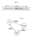
- Fig. 2 shows a demodulated signal eye diagram of a three-level AM/PSK signaling format. This is the signaling format which is used to carry data on the broadband network of Fig. 1.
- the eye diagram has specific sampling times identified by the arrows pointing downwards.
- the diagram also has a data 1 level, a code violation level, and a data 0 level. Data 1 level and data 0 level are dedicated for carrying data 1 and 0, respectively. Similarly, the code violation level positioned midway of data 1 and 0 levels is used for carrying code violations. As stated above, this code violation is often referred to as the non-data information.
- Figs. 7A and 7B show two graphical representations of a binary signaling and ternary signaling format.
- the amplitude of the carrier has three possible levels which are designated as 0, 2, and 4.
- the baseband digital symbol set has three signal elements; that is, data 1, data 0 or simply, 0, 1 and non-data.
- the symbols data 0 and data 1 are amplitude modulated to 0 and 4 carrier amplitudes, respectively, except for a special case which will be discussed later.
- the non-data symbols are always amplitude modulated to (2) carrier amplitude.
- non-data symbols always occur in pairs which is an inherent characteristic of the duobinary signaling method.
- the non-data symbols are used to indicate frame delimiters and to break up long sequences of identical data signals to keep the clock recovery circuit in the demodulator synchronized.
- the main advantage of this technique is its simplicity and higher transmission rate compared with other schemes employing no-data symbols such as bit stuffing, or n to (n+1) bit conversion.
- the major disadvantage of this technique is the increased vulnerability to noise.
- a comparison of Figs. 7A and 7B shows that the noise immunity is reduced by one-half or approximately 6 dB when compared with a system having no non-data symbols.
- the invention to be described subsequently accomplishes error correction by using the following apriori information and the occurrence of non-data symbols in the received signal.
- Fig. 3 shows a graphical representation of the proposed frame format which will be used to transport data on the broadband network.
- the frame comprises a preamble field, an SDEL field, an information field, an EDEL field. Successive frames are separated by idle patterns.
- the non-data symbols which are transmitted within a frame are placed in the SDEL and/or EDEL fields.
- a demodulator state diagram is shown. This diagram is helpful in understanding the various states that the demodulator goes through and the pattern it is searching for in each state.
- S0 This is an idle state, and the demodulator is looking for the preamble pattern.
- S1 the modulator moves into the initialization state (S1).
- S1 the modulator is searching for the SDEL pattern.
- S2 the receive state
- S2 the modulator looks for the EDEL pattern.
- the frame is completed and the demodulator moves back into the idle state.
- Fig. 5 shows a block diagram of the error correcting scheme according to the teaching of the present invention.
- the circuit arrangement includes two thresholders labeled thresholder 1 (TH1) and thresholder 2 (TH2).
- the thresholders output data and non-data, on separate conductors, to error detection/correction circuit means 16.
- Two signals identified as error corrected data out and error corrected non-data out are delivered to the medium access control MAC layer.
- a signal called recovered symbol clock is extracted from the received frame and is supplied to the error correction circuit means 16.
- the signal which is received (labeled in Fig. 5 as a received signal In) may either be at a level 0, 2 or 4.
- the signal at levels 4 and 0 are data signals while the signal at level 2 represents non-data (that is, code violation, non-code violation) symbols.
- thresholder 2 is to make non-data or no non-data decisions. It should be noted that the probability of error of thresholder 1 is the same as a binary system when symbol (0) or (4) is received. The probability of error of thresholder 2 is much higher and is independent of whether the received symbol is (0), (2), or (4).
- the error correction is done using pattern matching and windowing to detect non-data symbols and correcting them when necessary. As pointed out above in conjunction with the description of Fig. 4, the template used in the pattern matching is determined by the state of the demodulator.
- Figs. 6, 6A, 6B and 6C show one embodiment of the error correction circuit means 16.
- the implementation in Figs. 6, 6A, 6B and 6C does not preclude other equivalent implementations in hardware or software or in some combination of both. Suffice it to say that the error correction algorithm (to be described later) monitors the incoming data stream and depending upon the received pattern the demodulator makes changes or no changes to the received data which is subsequently transmitted up to the MAC layer.
- the hardware embodiment shown in Figs. 6, 6A, 6B and 6C uses two 8-bit shift registers SR1 and SR2, one divider by 8 binary counters (C1), 8 flip-flops (either set/reset or D-type F1-F8), 13 AND gates, and 7 OR gate.
- the outputs from the two thresholders are inputted into the shift registers as shown in Figs. 6, 6A, 6B and 6C.
- F1, F2, and C1 are in a reset state.
- a reception of a burst of data starts by detecting a preamble.
- a preamble is a 32 symbol pattern of alternating 4 and 0 which is optimum for fast clock recovery and automatic gain control capture in the demodulator.
- a preamble is detected when an 8-bit sequence of alternating 4 And 0's are received as indicated by AND gate 6.
- the output of AND gate 6 is latched in F1 which in turn enables A1 so that received data symbols (labeled DATA OUT) are transferred to the next higher layer (that is, the medium access control, MAC, layer). After the preamble is detected, the error correction circuit starts searching for an SDEL.
- the bit pattern for an SDEL is (non-data, non-data, 0, non-data, non-data, 0, 0, 0).
- the SDEL bit pattern may also be represented as (CV, CV, 0, CV, CV, 0, 0, 0) where CV represents code violation. In the last representation the non-data notation is replaced with code violation (CV) notation.
- An SDEL is detected if at least one symbol from each pair of non-data symbols is detected correctly and all other data signals are detected correctly. The probability of misses and false alarms of this procedure is as follows: p e (miss) ⁇ 2 . p (both symbols in a non-data pair are not detected) ⁇ 2 .
- the above error probability should have a negligible impact on the system throughput performance since the shortest packet (token packet) has a couple hundred bits, and, therefore, the probability that the information field has at least one error is greater than 10 ⁇ 6, which is much larger than the probability of error in detecting an SDEL.
- the SDEL is detected by AND gate 7 which sets latch F2 which in turn sets F3.
- the output from F3 is gated by AND gate 2 and starts the binary counter C1.
- the carry output from C1 is now the octet clock.
- the correct non-data symbol pattern is sent to the MAC layer by the error correction circuit. This is done by finding the correct non-data symbol position in the SDEL octet field by decoding the binary counter output (A,B, and C with AND gates 3, 4, 5, and OR gate 4.
- a non-data symbol is sent to MAC layer at the correct positions in the octet through AND gate 14 and OR gate 7.
- the EDEL has (non-data, non-data, 1, non-data, non-data, 1, 0, X) bit pattern; where X denotes a don't care state.
- the EDEL is detected using the same algorithm used for the SDEL; that is, an EDEL is detected if at least one non-data symbol from each non-data pair is detected correctly with small data symbols detected without error.
- the probability of missed and false alarms for EDEL is as follows: p e (miss) ⁇ 2 . p ecv 2 p e (false alarm) ⁇ p(2 data bits are detected as non-data's) ⁇ p ecv 2
- an EDEL is detected by AND gate 8 and latched in F5 which enables And 14 so that the correct non-data pattern is sent to the MAC layer.
- An EDEL indicates the end of the current burst.
- the error correction circuit arrangement is reset to detect the next preamble and so forth. This is accomplished by resetting F5 after sending error corrected EDEL to the MAC layer which in turn resets F1 which resets F2 and C1 subsequently.
- non-data symbols are also used to indicate a fourth type of transition which is used to break up a long string of the same data symbols.
- the error correction circuit (Figs. 6, 6A, 6B and 6C) searches for patterns with 13 same data symbols followed by a complement symbol aligned with an octet boundary.
- the output of TH2 (non-data threshold) (Fig. 5) of the corresponding position is sent to the MAC layer.
- the technique may be characterized as a moving window scheme where the window is being opened only when non-data signals are supposed to be in the transmitted frame.
- AND gate 9 and AND gate 10 are used to detect octets having the same or identical symbols.
- F7 is set and the symbol type is latched in F8.
- AND gate 11 or AND gate 12 is enabled which in turn enables AND gate 13 during the last two symbol positions of the second octet and the corresponding non-data outputs are sent to the MAC layer.
- the error correction algorithm may be summarized in the following steps:
- thresholder 1 To detect the EDEL, monitor successive octets from thresholder 1 and thresholder 2 simultaneously.
- the same algorithm used in detecting the SDEL is used except that the valid bit sequence from a thresholder 1 is (X,X,1,X,X,1,0,X).
- the MAC layer When a valid EDEL is detected, the MAC layer is notified by sending the correct EDEL.
- thresholder 2 When two consecutive octets having no transition in the first 13-bit position is followed by a transition, in the fourteenth position the output of thresholder 2 is examined. If the last two bits of the octet from thresholder 2 are (1,1), then the present octet is assumed to have no transitions and the output from thresholder 1 will be modified before being sent to the MAC layer. Otherwise, the output from thresholder 1 is sent without modification.
- the required signal-to-noise ratio of the transmitted data is significantly reduced.
Abstract
Description
- The invention relates to the detection and correction of errors in information processing and, more particularly, to detection and correction of errors in signals transmitted on a broadband network utilizing a three-level duobinary AM/PSK coding format.
- Error detecting and correcting techniques for processing information are well known in the prior art. Most error detecting and correcting techniques are directly related to the type of coding technique used to handle the data. U.S. Patent 4,118,686 describes an isolated (single) error correction scheme for processing data that is coded with a modified duobinary code. The error detection technique uses the special properties associated with this specific code to identify and correct an error. Error correction is predicated on the concept of maximum likelihood of error for the bit having the maximum amplitude variation from the corresponding nominal amplitude level.
- U.S. Patent 3,418,631 describes an error detection technique for information coded with a paired selected ternary (PST) code. In particular, the technique detects transmission errors that introduce a non-zero DC component. The non-zero DC component may cause a serious problem if accumulated over a tandem connection of many transmission channels which cannot transmit DC or low frequency components of a signal. Specific properties of the PST code are utilized to identify the unwanted condition. The detected error bits are replaced with a unique code having no DC component. The frequency of occurrence of this code is used to monitor the status of each link in tandem connection.
- U.S. Patent 4,276,649 describes a technique for minimizing the noise due to transmission errors in digitized voice systems. The technique is especially effective for delta modulation systems. This is done by detecting the error in the form of code violations in bipolar coded signals (alternate mark inversion code) and generating idle channel noise when error is detected.
- U.S. Patent 3,866,147 describes a technique for implementing a correlated ternary code. The code is claimed to have a power spectral density similar to a duobinary code but has more data transitions which can be used for clock recovery in the receiver. Error detection is based on the specific properties of the code.
- Recently, the IEEE Local Area Network (Project 802.4) has proposed new standards for allowing a token passing multiple access scheme on a broadband network. The scheme uses duobinary AM/PSK modulation to achieve 5 Mb/sec data rate in a 6 MHz channel. A ternary signaling convention is proposed. Compared with a binary signaling format, ternary signaling format is more susceptible to noise. In terms of a bit error rate (BER) versus signal-to-noise ratio (SNR), ternary signaling requires 6 dB higher signal-to-noise ratio compared with binary signaling. The higher SNR requirement raises a problem in that the system is more vulnerable to transmission errors caused by noise in the broadband network. (Note that in broadband network, the signal power cannot be increased beyond a certain maximum power level without affecting other signals sharing the broadband network.)
- It is therefore the main object of the present invention to provide a novel technique and apparatus for processing data transmitted in accordance with the above proposed standard. The novel technique provides a significant reduction in the SNR requirement.
- The novel technique includes an error correction algorithm which is selectively applied to a data frame at the proposed physical (transmission) layer.
- It comprises the steps of:
- (a) generating a first stream of electrical signals representing transmitted data;
- (b) generating a second stream of electrical signals representing transmitted code violation (CV) and/or non-code violation (CV) information;
- (c) analyzing the electrical signals to identify a first predetermined bit pattern representing a field within an information frame;
- (d) analyzing the electrical signals to identify a second predetermined bit pattern representing a field within said information frame;
- (e) searching the second predetermined bit pattern for a predetermined number of occurrences of a special character set contained in said second predetermined bit pattern; and
- (f) sending said second predetermined bit pattern as a special control field to the next layer of a layered architecture only if the predetermined number of occurrences of said special character set is being found in the second predetermined bit pattern.
- The apparatus includes two thresholding devices. One of the thresholding devices is used to make the normal data (1, 0) decision. The other thresholding device is used to make non-data or code violation (CV) decision. The non-data decision includes CV and non-code violations (). A correlation means is provided to examine the transmission packet outputted from the thresholding device. Relying on certain characteristics of the code the algorithm in the correlation means searches for specific bit patterns (to be described later). The desired bit patterns, if present, can only be located in certain fields of the incoming packet. When the bit pattern is found in the predetermined field, the field is forwarded to a higher layer for further processing. If the bit pattern is not found due to transmission error, it is written into the known position of the field (error correction) and the field is then forwarded to the higher layer.

-
- Fig. 1 shows a simplified conceptual broadband communications network in which the present invention can be used.
- Fig. 2 shows a graph (eye diagram) for a demodulated 3-level AM/PSK signal format.
- Fig. 3 shows a graph for the IEEE 802.4 token bus frame format.
- Fig. 4 shows a state diagram for a demodulator according to the teachings of the present invention.
- Fig. 5 shows the error correcting circuit arrangement according to the teaching of the present invention.
- Fig. 6 shows a hardware implementation for the error correcting scheme.
- Fig. 7 shows a graphical representation for nominal signal levels and threshold voltages for binary and ternary signaling formats.
- Fig. 1 shows a broadband or CATV communications network in which the present invention can be adapted. Broadband networks are designed primarily for analog video signal transmission, but can also be used to transmit data. The broadband network comprises of a
forward signal path 10, areverse signal path 12 and a headend 14 interconnecting both paths. A plurality of information sources labeled S₁-Sn are connected to the reverse path of the network. Likewise, a plurality of information sources labeled sink₁-sinkn are connected to the sources and to theforward path 10 of the network. It is worthwhile noting that a broadband network provides a very large bandwidth (300-400 MHZ) which can be shared among many users and applications using, for example, frequency division multiplexing or any other conventional techniques. - To transmit data through a broadband network, the information source which may be a data terminal, a computer, etc. transmits data on the
reverse path 12 to theheadend 14. Usually, the data from the information source utilizes a digital format. The headend wraps the data around and retransmits the data on the forward path to the information sinks. The broadband network cannot handle the baseband digital formatted data directly and, therefore, it is necessary to modulate the baseband digital data from the information source into a radio frequency signal before it is transmitted on the reverse path. The selected radio frequency signal should lie within the passband of the reverse channel and forward channel. The information sinks demodulate the received RF signal back to baseband digital data and delivers it to the respective sources. - Depending on the network configuration, the
headend 14 may perform not only amplification but also frequency translation (for a single cable system), and/or remodulation where the received signal is demodulated to baseband digital signal and then modulated again. This approach provides a cleaner signal for the demodulators and establishes a central point where sophisticated network management functions can reside. The present invention (to be described subsequently) can be used with any headend configuration. - Fig. 2 shows a demodulated signal eye diagram of a three-level AM/PSK signaling format. This is the signaling format which is used to carry data on the broadband network of Fig. 1. The eye diagram has specific sampling times identified by the arrows pointing downwards. The diagram also has a
data 1 level, a code violation level, and adata 0 level.Data 1 level anddata 0 level are dedicated for carryingdata data - Figs. 7A and 7B show two graphical representations of a binary signaling and ternary signaling format. In the proposed ternary signaling format (Fig. 7B), the amplitude of the carrier has three possible levels which are designated as 0, 2, and 4. The baseband digital symbol set has three signal elements; that is,
data 1,data 0 or simply, 0, 1 and non-data. Thesymbols data 0 anddata 1 are amplitude modulated to 0 and 4 carrier amplitudes, respectively, except for a special case which will be discussed later. The non-data symbols are always amplitude modulated to (2) carrier amplitude. In addition, non-data symbols always occur in pairs which is an inherent characteristic of the duobinary signaling method. - In the proposed physical layer standard, the non-data symbols are used to indicate frame delimiters and to break up long sequences of identical data signals to keep the clock recovery circuit in the demodulator synchronized. The main advantage of this technique is its simplicity and higher transmission rate compared with other schemes employing no-data symbols such as bit stuffing, or n to (n+1) bit conversion. As pointed out above, the major disadvantage of this technique is the increased vulnerability to noise. A comparison of Figs. 7A and 7B shows that the noise immunity is reduced by one-half or approximately 6 dB when compared with a system having no non-data symbols.
- The invention to be described subsequently accomplishes error correction by using the following apriori information and the occurrence of non-data symbols in the received signal.
- 1. Non-data symbols occur only rarely. They occur only in start delimiters (SDEL), end delimiters (EDEL), and to indicate a forced transition that breaks up two consecutive octets (1 octet = 8 symbols) of the same symbol. The SDEL and EDEL will be described subsequently.
- 2. Non-data symbols always occur in pairs.
- 3. Once the octet synchronization is achieved by detecting an SDEL, the possible non-data positions in an octet are known.
- Fig. 3 shows a graphical representation of the proposed frame format which will be used to transport data on the broadband network. The frame comprises a preamble field, an SDEL field, an information field, an EDEL field. Successive frames are separated by idle patterns. As stated before, the non-data symbols which are transmitted within a frame are placed in the SDEL and/or EDEL fields. By monitoring the incoming data to determine the presence of code violation in these fields, the demodulator can easily perform error correction if the expected code violations are not included in a received message.
- Turning to Fig. 4 for a moment, a demodulator state diagram is shown. This diagram is helpful in understanding the various states that the demodulator goes through and the pattern it is searching for in each state. At the beginning of a cycle the modulator is in state S₀. This is an idle state, and the demodulator is looking for the preamble pattern. When the preamble is detected, the modulator moves into the initialization state (S₁). In state (S₁) the modulator is searching for the SDEL pattern. When the SDEL pattern is detected, the modulator moves into the receive state (S₂). In the receive state the modulator looks for the EDEL pattern. When that pattern is detected, the frame is completed and the demodulator moves back into the idle state.
- Fig. 5 shows a block diagram of the error correcting scheme according to the teaching of the present invention. The circuit arrangement includes two thresholders labeled thresholder 1 (TH1) and thresholder 2 (TH2). The thresholders output data and non-data, on separate conductors, to error detection/correction circuit means 16. Two signals identified as error corrected data out and error corrected non-data out are delivered to the medium access control MAC layer. A signal called recovered symbol clock is extracted from the received frame and is supplied to the error correction circuit means 16. As stated before, with reference to Figs. 7A and 7B, the signal which is received (labeled in Fig. 5 as a received signal In) may either be at a
level levels level 2 represents non-data (that is, code violation, non-code violation) symbols. - The thresholder 1 (Fig. 5) includes
comparator 18. The conductor labeled received signal In is tied to the positive input to the comparator and the negative input of the comparator is tied to threshold voltage VTH1=2. Thethresholder 1 makesdata 1 ordata 0 decisions. The thresholder 2 (TH2) has two comparators identified bynumerals Comparator 20 has its negative terminal connected to Receive Signal In while the positive terminal is tied to threshold voltage VTH2=3. Similarly,Comparator 22 has its positive terminal tied to the Receive Signal In and its negative terminal ties to threshold voltage VTH3=1. It should be noted that the various threshold levels are chosen in accordance with the graphical representation shown in Fig. 7B. - As stated before, the function of
thresholder 2 is to make non-data or no non-data decisions. It should be noted that the probability of error ofthresholder 1 is the same as a binary system when symbol (0) or (4) is received. The probability of error ofthresholder 2 is much higher and is independent of whether the received symbol is (0), (2), or (4). The error correction is done using pattern matching and windowing to detect non-data symbols and correcting them when necessary. As pointed out above in conjunction with the description of Fig. 4, the template used in the pattern matching is determined by the state of the demodulator. - Figs. 6, 6A, 6B and 6C show one embodiment of the error correction circuit means 16. The implementation in Figs. 6, 6A, 6B and 6C does not preclude other equivalent implementations in hardware or software or in some combination of both. Suffice it to say that the error correction algorithm (to be described later) monitors the incoming data stream and depending upon the received pattern the demodulator makes changes or no changes to the received data which is subsequently transmitted up to the MAC layer. The hardware embodiment shown in Figs. 6, 6A, 6B and 6C uses two 8-bit shift registers SR1 and SR2, one divider by 8 binary counters (C1), 8 flip-flops (either set/reset or D-type F1-F8), 13 AND gates, and 7 OR gate. The interconnection between the named circuit modules are clearly shown in the Figs. Since each of these items is clearly identified and the interconnection between each item is clearly shown in the figure, the remaining portion of this application will be devoted to how the system works rather than how it is connected relative to each part. It is believed that this approach will minimize the size and complexity of the application.
- The outputs from the two thresholders (Fig. 5) are inputted into the shift registers as shown in Figs. 6, 6A, 6B and 6C. During idle (that is, no packets are being received on the bus) F1, F2, and C1 are in a reset state. A reception of a burst of data starts by detecting a preamble. A preamble is a 32 symbol pattern of alternating 4 and 0 which is optimum for fast clock recovery and automatic gain control capture in the demodulator. In the present scheme a preamble is detected when an 8-bit sequence of alternating 4 And 0's are received as indicated by AND
gate 6. The output of ANDgate 6 is latched in F1 which in turn enables A1 so that received data symbols (labeled DATA OUT) are transferred to the next higher layer (that is, the medium access control, MAC, layer). After the preamble is detected, the error correction circuit starts searching for an SDEL. - The bit pattern for an SDEL is (non-data, non-data, 0, non-data, non-data, 0, 0, 0). The SDEL bit pattern may also be represented as (CV, CV, 0, CV, CV, 0, 0, 0) where CV represents code violation. In the last representation the non-data notation is replaced with code violation (CV) notation. An SDEL is detected if at least one symbol from each pair of non-data symbols is detected correctly and all other data signals are detected correctly. The probability of misses and false alarms of this procedure is as follows:
pe(miss) ≃ 2 . p (both symbols in a non-data pair are not detected)
≃ 2 .p ecv²
pe(false alarm) ≃ p(preamble is detected as SDEL)
= p(twodata 1's are detected as 0's)
=p ed² «pe(miss)
where pecv is the probability of error of thresholder TH2 and ped is the probability of error of thresholder TH1 respectively. - If we choose pe(miss) ≃ 10⁻⁸, then we have pecv ≃ 10⁻⁴ and the required SNR is decreased approximately by 4 dB. The theoretical BER vs. required SNR for the 2-level AM/PSK system is given in the appendix.
- The above error probability (miss and flase alarm in detecting an SDEL) should have a negligible impact on the system throughput performance since the shortest packet (token packet) has a couple hundred bits, and, therefore, the probability that the information field has at least one error is greater than 10⁻⁶, which is much larger than the probability of error in detecting an SDEL.
- Still referring to Figs. 6, 6A, 6B and 6C, the SDEL is detected by AND
gate 7 which sets latch F2 which in turn sets F3. The output from F3 is gated by ANDgate 2 and starts the binary counter C1. The carry output from C1 is now the octet clock. When an SDEL is detected, the correct non-data symbol pattern is sent to the MAC layer by the error correction circuit. This is done by finding the correct non-data symbol position in the SDEL octet field by decoding the binary counter output (A,B, and C with ANDgates OR gate 4. A non-data symbol is sent to MAC layer at the correct positions in the octet through ANDgate 14 andOR gate 7. Since the EDEL octet has non-data symbols in the same position as SDEL, the same decoding circuit is used in EDEL correction. F4 (Fig. 6C) ensures that only one SDEL non-data pattern is sent to the MAC layer during a burst. - The EDEL has (non-data, non-data, 1, non-data, non-data, 1, 0, X) bit pattern; where X denotes a don't care state. The EDEL is detected using the same algorithm used for the SDEL; that is, an EDEL is detected if at least one non-data symbol from each non-data pair is detected correctly with small data symbols detected without error. The probability of missed and false alarms for EDEL is as follows:
pe(miss) ≃ 2 .p ecv²
pe(false alarm) ≃ p(2 data bits are detected as non-data's)
≃ p ecv² - It should be noted that the probability of error in detecting an EDEL is about the same as that of an SDEL. With reference to Figs. 6, 6A, 6B and 6C, an EDEL is detected by AND
gate 8 and latched in F5 which enables And 14 so that the correct non-data pattern is sent to the MAC layer. An EDEL indicates the end of the current burst. After sending an EDEL to the MAC layer, the error correction circuit arrangement is reset to detect the next preamble and so forth. This is accomplished by resetting F5 after sending error corrected EDEL to the MAC layer which in turn resets F1 which resets F2 and C1 subsequently. - As was mentioned previously, non-data symbols are also used to indicate a fourth type of transition which is used to break up a long string of the same data symbols. When two successive octets have no transition, the last three symbols in the second octet are replaced by (transition, non-data, non-data) where transition indicates the complement symbol. The error correction circuit (Figs. 6, 6A, 6B and 6C) searches for patterns with 13 same data symbols followed by a complement symbol aligned with an octet boundary. When such pattern is detected, the output of TH2 (non-data threshold) (Fig. 5) of the corresponding position (that is, the last two symbol positions) is sent to the MAC layer. The technique may be characterized as a moving window scheme where the window is being opened only when non-data signals are supposed to be in the transmitted frame.
- The rule used to detect non-data symbols following a forced data transition is to require that both non-data symbols in the pair should be correctly detected. Then the conditional error probability on the condition of a single transition following 13 consecutive bit times of no transition are:
p(miss) = p (at least one non-data is not detected)
≃ pecv p(false alarm) = p(two non-data's are detected falsely)
=p ecv² - The probability of an occurrence of such data pattern is small (< 10⁻⁵) since scrambling or randomizing of data symbols is required by the standard, and therefore, the impact of these error probabilities on the system performance is also negligible.
- In Figs. 6, 6A, 6B and 6C, AND
gate 9 and ANDgate 10 are used to detect octets having the same or identical symbols. When an octet is found to have all the same symbols, F7 is set and the symbol type is latched in F8. When the next octet has the correct pattern, ANDgate 11 or ANDgate 12 is enabled which in turn enables AND gate 13 during the last two symbol positions of the second octet and the corresponding non-data outputs are sent to the MAC layer. The above analysis clearly shows that the error correction method of the present invention provides octet error probability roughly equal to a 2-level system operating at 10⁻⁸ bit error rate with about 2 decibel (dB) increase in signal-to-noise ratio rather than 6 decibels. - The error correction algorithm, according to the teaching of the present invention, may be summarized in the following steps:
- Step 1: Monitor contiguous 8-bits of the output of
thresholder 1, data thresholder, Figs. 6, 6A, 6B and 6C until a preamble is received. A valid preamble has the sequence of (4,0,4,0,4,0,4,0,). - Step 2: Upon detecting a preamble, look for a start delimiter (SDEL) by monitoring contiguous 8-bits of the outputs from thresholder 1 (data thresholder) and thresholder 2 (non-data thresholder) simultaneously. The error-free SDEL is a sequence (CV, CV, 0, CV, CV, 0 0 0). A valid SDEL is detected if the output from
thresholder 1 has the sequence (X,X,0,X,X,0,0,0) and the output ofthresholder 2 has at least one (1) in each pair of CV positions, that is, in bit position (0, 1) and (3, 4). There are a total of nine valid sequences. X indicates a don't care state. - Step 3: Upon detecting a valid SDEL, the octet clock (C1) is started. The SDEL is sent to the MAC layer after error correction (if necessary). From this point on we look for an end delimiter (EDEL) and data pattern which has no transition in two consecutive octets. This is done as follows:
- To detect the EDEL, monitor successive octets from
thresholder 1 andthresholder 2 simultaneously. The same algorithm used in detecting the SDEL is used except that the valid bit sequence from athresholder 1 is (X,X,1,X,X,1,0,X). When a valid EDEL is detected, the MAC layer is notified by sending the correct EDEL. - When two consecutive octets having no transition in the first 13-bit position is followed by a transition, in the fourteenth position the output of
thresholder 2 is examined. If the last two bits of the octet fromthresholder 2 are (1,1), then the present octet is assumed to have no transitions and the output fromthresholder 1 will be modified before being sent to the MAC layer. Otherwise, the output fromthresholder 1 is sent without modification. - By using the above invention, the required signal-to-noise ratio of the transmitted data is significantly reduced.
Claims (8)
Applications Claiming Priority (2)
| Application Number | Priority Date | Filing Date | Title |
|---|---|---|---|
| US741400 | 1985-06-05 | ||
| US06/741,400 US4677627A (en) | 1985-06-05 | 1985-06-05 | Error correction scheme |
Publications (3)
| Publication Number | Publication Date |
|---|---|
| EP0207243A2 true EP0207243A2 (en) | 1987-01-07 |
| EP0207243A3 EP0207243A3 (en) | 1988-10-19 |
| EP0207243B1 EP0207243B1 (en) | 1992-07-08 |
Family
ID=24980581
Family Applications (1)
| Application Number | Title | Priority Date | Filing Date |
|---|---|---|---|
| EP86105484A Expired EP0207243B1 (en) | 1985-06-05 | 1986-04-21 | Error correction mechanism |
Country Status (5)
| Country | Link |
|---|---|
| US (1) | US4677627A (en) |
| EP (1) | EP0207243B1 (en) |
| JP (1) | JPS61281721A (en) |
| CA (1) | CA1233233A (en) |
| DE (1) | DE3685914T2 (en) |
Cited By (6)
| Publication number | Priority date | Publication date | Assignee | Title |
|---|---|---|---|---|
| WO1990004295A1 (en) * | 1988-10-14 | 1990-04-19 | Concord Communications, Inc. | Symbol detection and error correction coding in a local area network |
| EP0461103A2 (en) * | 1990-06-01 | 1991-12-11 | Schrack Telecom-Aktiengesellschaft | Method to reduce adjacent channel interference by baseband coding |
| EP0505657A1 (en) * | 1991-03-27 | 1992-09-30 | International Business Machines Corporation | Preamble recognition and synchronization detection in partial-response systems |
| WO1992017966A1 (en) * | 1991-03-29 | 1992-10-15 | Raynet Corporation | Clamping receiver and transmission protocol |
| US6108808A (en) * | 1990-11-12 | 2000-08-22 | Texas Instruments Incorporated | Apparatus and method for decoding received signals and localization of errors therein by comparison with aberrant data values |
| EP1265409A1 (en) * | 2001-06-05 | 2002-12-11 | Alcatel | Decision circuit with multiplexed XOR gates |
Families Citing this family (8)
| Publication number | Priority date | Publication date | Assignee | Title |
|---|---|---|---|---|
| CA1258130A (en) * | 1985-07-11 | 1989-08-01 | Nec Corporation | Cmi signal transmission system |
| US5084903A (en) * | 1989-02-28 | 1992-01-28 | First Pacific Networks | Modulation and demodulation system employing AM-PSK and QPSK communication system using digital signals |
| JP3133490B2 (en) * | 1991-08-27 | 2001-02-05 | 古河電気工業株式会社 | Multiplex transmission equipment |
| US5424881A (en) | 1993-02-01 | 1995-06-13 | Cirrus Logic, Inc. | Synchronous read channel |
| US6185649B1 (en) * | 1998-05-19 | 2001-02-06 | Toshiba America Electronic Components, Inc. | System for correcting an illegal addressing signal by changing a current bit from one to zero if a bit immediately left adjacent to the current bit is zero |
| US6209108B1 (en) * | 1999-08-27 | 2001-03-27 | Qwest Communications International Inc. | Method for testing VDSL loops |
| US7149938B1 (en) * | 2001-12-07 | 2006-12-12 | Applied Micro Circuits Corporation | Non-causal channel equalization |
| US20060059411A1 (en) * | 2004-09-16 | 2006-03-16 | Sony Corporation And Sony Electronics, Inc. | Method and system for increasing channel coding gain |
Citations (1)
| Publication number | Priority date | Publication date | Assignee | Title |
|---|---|---|---|---|
| US4118686A (en) * | 1977-09-06 | 1978-10-03 | Gte Automatic Electric Laboratories, Incorporated | Error correction for signals employing the modified duobinary code |
Family Cites Families (5)
| Publication number | Priority date | Publication date | Assignee | Title |
|---|---|---|---|---|
| DE3069679D1 (en) * | 1980-12-08 | 1985-01-03 | Ibm | Method of transmitting information between stations attached to a unidirectional transmission ring |
| US4507777A (en) * | 1983-02-03 | 1985-03-26 | International Business Machines Corporation | Protocol for determining physical order of active stations on a token ring |
| US4556974A (en) * | 1983-10-07 | 1985-12-03 | Honeywell Inc. | Method for passing a token in a local-area network |
| US4566097A (en) * | 1983-12-23 | 1986-01-21 | International Business Machines Corp. | Token ring with secondary transmit opportunities |
| US4549292A (en) * | 1984-02-17 | 1985-10-22 | Burroughs Corporation | Method of efficiently and simultaneously transmitting both isochronous and nonisochronous data in a computer network |
-
1985
- 1985-06-05 US US06/741,400 patent/US4677627A/en not_active Expired - Fee Related
-
1986
- 1986-04-18 JP JP61088418A patent/JPS61281721A/en active Granted
- 1986-04-21 EP EP86105484A patent/EP0207243B1/en not_active Expired
- 1986-04-21 DE DE8686105484T patent/DE3685914T2/en not_active Expired - Fee Related
- 1986-05-28 CA CA000510245A patent/CA1233233A/en not_active Expired
Patent Citations (1)
| Publication number | Priority date | Publication date | Assignee | Title |
|---|---|---|---|---|
| US4118686A (en) * | 1977-09-06 | 1978-10-03 | Gte Automatic Electric Laboratories, Incorporated | Error correction for signals employing the modified duobinary code |
Non-Patent Citations (1)
| Title |
|---|
| DATA COMMUNICATIONS, vol. 12, no. 6, June 1983, pages 225-227, New York, US; D.V. RATNER: "How broadband modems operate on token-passing nets" * |
Cited By (8)
| Publication number | Priority date | Publication date | Assignee | Title |
|---|---|---|---|---|
| WO1990004295A1 (en) * | 1988-10-14 | 1990-04-19 | Concord Communications, Inc. | Symbol detection and error correction coding in a local area network |
| US5099500A (en) * | 1988-10-14 | 1992-03-24 | Concord Communications, Inc. | Symbol detection and error correction coding in a local area network |
| EP0461103A2 (en) * | 1990-06-01 | 1991-12-11 | Schrack Telecom-Aktiengesellschaft | Method to reduce adjacent channel interference by baseband coding |
| EP0461103A3 (en) * | 1990-06-01 | 1993-01-20 | Schrack Telecom-Aktiengesellschaft | Method to reduce adjacent channel interference by baseband coding |
| US6108808A (en) * | 1990-11-12 | 2000-08-22 | Texas Instruments Incorporated | Apparatus and method for decoding received signals and localization of errors therein by comparison with aberrant data values |
| EP0505657A1 (en) * | 1991-03-27 | 1992-09-30 | International Business Machines Corporation | Preamble recognition and synchronization detection in partial-response systems |
| WO1992017966A1 (en) * | 1991-03-29 | 1992-10-15 | Raynet Corporation | Clamping receiver and transmission protocol |
| EP1265409A1 (en) * | 2001-06-05 | 2002-12-11 | Alcatel | Decision circuit with multiplexed XOR gates |
Also Published As
| Publication number | Publication date |
|---|---|
| JPH0258816B2 (en) | 1990-12-10 |
| EP0207243A3 (en) | 1988-10-19 |
| CA1233233A (en) | 1988-02-23 |
| DE3685914D1 (en) | 1992-08-13 |
| EP0207243B1 (en) | 1992-07-08 |
| DE3685914T2 (en) | 1993-02-25 |
| JPS61281721A (en) | 1986-12-12 |
| US4677627A (en) | 1987-06-30 |
Similar Documents
| Publication | Publication Date | Title |
|---|---|---|
| US4677627A (en) | Error correction scheme | |
| US7688864B2 (en) | Dynamic preamble detection | |
| US6618395B1 (en) | Physical coding sub-layer for transmission of data over multi-channel media | |
| US8065584B2 (en) | Transmitting data words | |
| US6859899B2 (en) | Method for data packet acquisition using split preamble | |
| EP0595034B1 (en) | Differentially coded and guard pulse position modulation for communication networks | |
| US6430230B1 (en) | Methods of encoding payload bits for transmission | |
| Masamura et al. | Differential detection of MSK with nonredundant error correction | |
| US6088827A (en) | 1000BASE-T packetized trellis coder | |
| US3950616A (en) | Alignment of bytes in a digital data bit stream | |
| JPH10215205A (en) | Receiver for direct spread spectrum | |
| US6539051B1 (en) | Parallel framer and transport protocol with distributed framing and continuous data | |
| KR20040097247A (en) | Synchronization data detection unit and method | |
| US5881074A (en) | 1000base-t packetized trellis coder | |
| JPH0556698B2 (en) | ||
| CN100367698C (en) | Sychronization data detection unit and method | |
| US5737357A (en) | Apparatus and method for data pattern sensitivity correction | |
| KR100466544B1 (en) | Method of correcting OFDM symbol error of digital audio broadcasting receiver and system of the same | |
| KR100227487B1 (en) | Field synchronization detection system in the hdtv | |
| Jones | Digital transmission | |
| Keogh | The state diagram of HDB3 | |
| JP2891444B2 (en) | Delay detection method | |
| JPS60154754A (en) | Transmitter-receiver of digital signal | |
| SU et al. | THE MLT-N LINE CODE AND MULTI-LEVEL BURST-MODE RECEIVER FOR MULTIACCESS LOCAL AREA NETWORKS | |
| Probst et al. | Bit and frame synchronization techniques |
Legal Events
| Date | Code | Title | Description |
|---|---|---|---|
| PUAI | Public reference made under article 153(3) epc to a published international application that has entered the european phase |
Free format text: ORIGINAL CODE: 0009012 |
|
| AK | Designated contracting states |
Kind code of ref document: A2 Designated state(s): DE FR GB IT |
|
| 17P | Request for examination filed |
Effective date: 19870422 |
|
| PUAL | Search report despatched |
Free format text: ORIGINAL CODE: 0009013 |
|
| AK | Designated contracting states |
Kind code of ref document: A3 Designated state(s): DE FR GB IT |
|
| 17Q | First examination report despatched |
Effective date: 19910102 |
|
| GRAA | (expected) grant |
Free format text: ORIGINAL CODE: 0009210 |
|
| AK | Designated contracting states |
Kind code of ref document: B1 Designated state(s): DE FR GB IT |
|
| PG25 | Lapsed in a contracting state [announced via postgrant information from national office to epo] |
Ref country code: IT Free format text: LAPSE BECAUSE OF FAILURE TO SUBMIT A TRANSLATION OF THE DESCRIPTION OR TO PAY THE FEE WITHIN THE PRE;WARNING: LAPSES OF ITALIAN PATENTS WITH EFFECTIVE DATE BEFORE 2007 MAY HAVE OCCURRED AT ANY TIME BEFORE 2007. THE CORRECT EFFECTIVE DATE MAY BE DIFFERENT FROM THE ONE RECORDED.SCRIBED TIME-LIMIT Effective date: 19920708 |
|
| REF | Corresponds to: |
Ref document number: 3685914 Country of ref document: DE Date of ref document: 19920813 |
|
| ET | Fr: translation filed | ||
| PGFP | Annual fee paid to national office [announced via postgrant information from national office to epo] |
Ref country code: GB Payment date: 19930324 Year of fee payment: 8 |
|
| PGFP | Annual fee paid to national office [announced via postgrant information from national office to epo] |
Ref country code: FR Payment date: 19930330 Year of fee payment: 8 |
|
| PGFP | Annual fee paid to national office [announced via postgrant information from national office to epo] |
Ref country code: DE Payment date: 19930428 Year of fee payment: 8 |
|
| PLBE | No opposition filed within time limit |
Free format text: ORIGINAL CODE: 0009261 |
|
| STAA | Information on the status of an ep patent application or granted ep patent |
Free format text: STATUS: NO OPPOSITION FILED WITHIN TIME LIMIT |
|
| 26N | No opposition filed | ||
| PG25 | Lapsed in a contracting state [announced via postgrant information from national office to epo] |
Ref country code: GB Effective date: 19940421 |
|
| GBPC | Gb: european patent ceased through non-payment of renewal fee |
Effective date: 19940421 |
|
| PG25 | Lapsed in a contracting state [announced via postgrant information from national office to epo] |
Ref country code: FR Effective date: 19941229 |
|
| PG25 | Lapsed in a contracting state [announced via postgrant information from national office to epo] |
Ref country code: DE Effective date: 19950103 |
|
| REG | Reference to a national code |
Ref country code: FR Ref legal event code: ST |