WO2008108926A1 - Apparatus and method for reducing edge effect in an image sensor - Google Patents
Apparatus and method for reducing edge effect in an image sensor Download PDFInfo
- Publication number
- WO2008108926A1 WO2008108926A1 PCT/US2008/002242 US2008002242W WO2008108926A1 WO 2008108926 A1 WO2008108926 A1 WO 2008108926A1 US 2008002242 W US2008002242 W US 2008002242W WO 2008108926 A1 WO2008108926 A1 WO 2008108926A1
- Authority
- WO
- WIPO (PCT)
- Prior art keywords
- pixels
- pixel
- dummy
- reset
- clear
- Prior art date
Links
- 238000000034 method Methods 0.000 title claims abstract description 25
- 230000000694 effects Effects 0.000 title claims abstract description 18
- 230000003287 optical effect Effects 0.000 claims abstract description 23
- 238000003491 array Methods 0.000 claims abstract description 18
- 238000003384 imaging method Methods 0.000 abstract description 22
- 230000001747 exhibiting effect Effects 0.000 abstract 1
- 238000012545 processing Methods 0.000 description 10
- 239000000969 carrier Substances 0.000 description 9
- 238000004519 manufacturing process Methods 0.000 description 9
- 238000009792 diffusion process Methods 0.000 description 8
- 239000000047 product Substances 0.000 description 8
- 230000015572 biosynthetic process Effects 0.000 description 6
- 230000008569 process Effects 0.000 description 5
- 230000004044 response Effects 0.000 description 5
- 238000005516 engineering process Methods 0.000 description 4
- 238000012986 modification Methods 0.000 description 4
- 230000004048 modification Effects 0.000 description 4
- 239000000758 substrate Substances 0.000 description 4
- 238000000137 annealing Methods 0.000 description 3
- 230000005540 biological transmission Effects 0.000 description 3
- 230000001976 improved effect Effects 0.000 description 3
- 238000002955 isolation Methods 0.000 description 3
- 239000002184 metal Substances 0.000 description 3
- 230000008093 supporting effect Effects 0.000 description 3
- 230000002939 deleterious effect Effects 0.000 description 2
- 238000000151 deposition Methods 0.000 description 2
- 239000006185 dispersion Substances 0.000 description 2
- 238000005286 illumination Methods 0.000 description 2
- 239000007943 implant Substances 0.000 description 2
- 230000006872 improvement Effects 0.000 description 2
- 150000002500 ions Chemical class 0.000 description 2
- 230000002093 peripheral effect Effects 0.000 description 2
- 238000005215 recombination Methods 0.000 description 2
- XUIMIQQOPSSXEZ-UHFFFAOYSA-N Silicon Chemical compound [Si] XUIMIQQOPSSXEZ-UHFFFAOYSA-N 0.000 description 1
- 238000009825 accumulation Methods 0.000 description 1
- 230000006978 adaptation Effects 0.000 description 1
- 230000002547 anomalous effect Effects 0.000 description 1
- 238000013459 approach Methods 0.000 description 1
- 230000000903 blocking effect Effects 0.000 description 1
- 230000003139 buffering effect Effects 0.000 description 1
- 239000006227 byproduct Substances 0.000 description 1
- 239000007795 chemical reaction product Substances 0.000 description 1
- 238000012937 correction Methods 0.000 description 1
- 230000008878 coupling Effects 0.000 description 1
- 238000010168 coupling process Methods 0.000 description 1
- 238000005859 coupling reaction Methods 0.000 description 1
- 238000013461 design Methods 0.000 description 1
- 238000010586 diagram Methods 0.000 description 1
- 238000007599 discharging Methods 0.000 description 1
- 230000007613 environmental effect Effects 0.000 description 1
- 230000002349 favourable effect Effects 0.000 description 1
- 230000001939 inductive effect Effects 0.000 description 1
- 230000010354 integration Effects 0.000 description 1
- 230000007246 mechanism Effects 0.000 description 1
- 238000001465 metallisation Methods 0.000 description 1
- 230000003278 mimic effect Effects 0.000 description 1
- 238000002161 passivation Methods 0.000 description 1
- 230000003094 perturbing effect Effects 0.000 description 1
- 230000035945 sensitivity Effects 0.000 description 1
- 229910052710 silicon Inorganic materials 0.000 description 1
- 239000010703 silicon Substances 0.000 description 1
- 238000000638 solvent extraction Methods 0.000 description 1
- 230000003595 spectral effect Effects 0.000 description 1
- 238000004544 sputter deposition Methods 0.000 description 1
- 230000006641 stabilisation Effects 0.000 description 1
- 238000011105 stabilization Methods 0.000 description 1
- 230000001629 suppression Effects 0.000 description 1
Classifications
-
- H—ELECTRICITY
- H01—ELECTRIC ELEMENTS
- H01L—SEMICONDUCTOR DEVICES NOT COVERED BY CLASS H10
- H01L27/00—Devices consisting of a plurality of semiconductor or other solid-state components formed in or on a common substrate
- H01L27/14—Devices consisting of a plurality of semiconductor or other solid-state components formed in or on a common substrate including semiconductor components sensitive to infrared radiation, light, electromagnetic radiation of shorter wavelength or corpuscular radiation and specially adapted either for the conversion of the energy of such radiation into electrical energy or for the control of electrical energy by such radiation
- H01L27/144—Devices controlled by radiation
- H01L27/146—Imager structures
- H01L27/14643—Photodiode arrays; MOS imagers
-
- H—ELECTRICITY
- H01—ELECTRIC ELEMENTS
- H01L—SEMICONDUCTOR DEVICES NOT COVERED BY CLASS H10
- H01L27/00—Devices consisting of a plurality of semiconductor or other solid-state components formed in or on a common substrate
- H01L27/14—Devices consisting of a plurality of semiconductor or other solid-state components formed in or on a common substrate including semiconductor components sensitive to infrared radiation, light, electromagnetic radiation of shorter wavelength or corpuscular radiation and specially adapted either for the conversion of the energy of such radiation into electrical energy or for the control of electrical energy by such radiation
- H01L27/144—Devices controlled by radiation
- H01L27/146—Imager structures
- H01L27/14601—Structural or functional details thereof
- H01L27/14609—Pixel-elements with integrated switching, control, storage or amplification elements
-
- H—ELECTRICITY
- H04—ELECTRIC COMMUNICATION TECHNIQUE
- H04N—PICTORIAL COMMUNICATION, e.g. TELEVISION
- H04N25/00—Circuitry of solid-state image sensors [SSIS]; Control thereof
- H04N25/60—Noise processing, e.g. detecting, correcting, reducing or removing noise
- H04N25/63—Noise processing, e.g. detecting, correcting, reducing or removing noise applied to dark current
-
- H—ELECTRICITY
- H01—ELECTRIC ELEMENTS
- H01L—SEMICONDUCTOR DEVICES NOT COVERED BY CLASS H10
- H01L27/00—Devices consisting of a plurality of semiconductor or other solid-state components formed in or on a common substrate
- H01L27/14—Devices consisting of a plurality of semiconductor or other solid-state components formed in or on a common substrate including semiconductor components sensitive to infrared radiation, light, electromagnetic radiation of shorter wavelength or corpuscular radiation and specially adapted either for the conversion of the energy of such radiation into electrical energy or for the control of electrical energy by such radiation
- H01L27/144—Devices controlled by radiation
- H01L27/146—Imager structures
- H01L27/14601—Structural or functional details thereof
- H01L27/14603—Special geometry or disposition of pixel-elements, address-lines or gate-electrodes
Definitions
- the present invention relates generally to image processing for electronic imaging sensors, and more particularly, to an apparatus and method for equalizing the dark current in pixels located on the periphery of an image sensor and thereby eliminating the so-called "edge effect" to optimize image quality.
- OB pixels are the reference pixels within an imaging sensor pixel array that should have virtually identical electrical characteristics as a standard active pixel, yet are insensitive to light.
- OB pixels are used by various image processing circuits in the sensor or camera to maintain a constant black level independent of gain, illumination, changes in sensor operating conditions, etc.
- An OB pixel's signal is normally processed using the same signal chain and timing as those that are photo-electrically responsive and form the image of interest.
- the latter pixels, which constitute the majority of pixels in an imaging sensor are some times referred to as "Clear Pixels.” While clear pixels form the actual image, OB pixels are indirectly used in the image formation process. Instead, OB pixels are used to track the environmental and operational status of the imaging sensor while also providing information regarding dark signal/current, column noise and line noise at the specific location of each OB pixel.
- OB pixels are typically used as reference pixels for many calibration operations that enhance image quality. These include black clamp stabilization, flutter rejection, column noise suppression and line noise correction. In these and other algorithms, OB pixels must have similar dark
- I 0 is the diode's saturation current
- V d is the diode voltage
- n is the diode ideality
- k is Boltzman's constant
- T is the Temperature.
- the saturation current can vary significantly from diode to diode.
- the Shockley equation can be alternately expressed:
- r ⁇ is the diode ideality for the specific diode and the parameter R 0 A is its resistance- area product at zero volts of applied bias, expressed in units of ohm-cm 2 . While diode resistance and saturation current depend on area, the R 0 A product fora specific technology is independent of area and characterizes the quality of diode fabrication. Different applications of an imaging sensor pixel array may require differing degrees of image quality. For instance, a CMOS sensor used in a studio broadcast camera to generate content for HDTV production (high-end application) requires significantly higher image quality than a CMOS sensor used in consumer camcorders (medium to low-end product application).
- the total current in clear, dummy and an OB pixel is the sum of each diode's Shockley-Read current, photocurrent and the electrical bias current; it is expressed as the direct sum:
- dummy pixels are disclosed that exhibit identical electrical characteristics to any other pixel in the imaging array. This insures that the total current of each dummy pixel used in an array also containing clear pixels and OB pixels is roughly identical to the total current of a clear pixel. While an OB pixel used as a reference for signal processing is read each frame, a dummy pixel must look the same even though it may never be read, regardless whether it is opaque or light- sensitive. Further, the dummy pixels do not perturb the electrical characteristics of nearby pixels so that they can be used to isolate the various sub-arrays that compose an imaging array. Such dummy pixels are also placed at the edges of the imaging array to prevent discontinuities stemming from process-related, physical and electrical factors. Edge effects are thereby eliminated.
- the preferred embodiment of the dummy pixel is a clear type with identical electrical characteristics to the clear pixels in the main imaging array.
- a second embodiment of the dummy pixel is optically black to support optional signal processing functions.
- Dummy OB pixels are constituted in the present invention by: 1) forming the pixels within a standard production process wherein the light- blocking property of the OB pixel is formed separately from basic diode formation including the various annealing steps that mitigate implant damage.
- An improved method for forming an Optical Black layer separately from the underlying CMOS sensor process is disclosed in U.S. Patent Application Serial No. 1 1/461,457, entitled IMAGE SENSOR AND METHOD FOR MANUFACTURING THE SAME, filed August 1, 2006, the disclosure of which is herein incorporated by reference in its entirety 2) partitioning the pixel array into sub-arrays of clear pixels, dummy pixels, and OB pixels that may be isolated from supporting peripheral circuits by N- guard band regions.
- the latter guard band regions collect stray minority carriers and prevent extraneous minority carriers from offsetting the OB reference signal.
- Such guard bands are used in areas adjacent to, for example, high speed digital circuits that emit light as a by-product of hot carrier effects.
- dummy OB pixel formation is completed by operating the dummy pixels with the reset transistor biased in soft reset mode to prevent signal integration. This insures low-noise operation and minimizes generation of excess generation-recombination currents that alter diode ideality and/or R 0 A product.
- Dummy clear pixel formation is completed by omitting step 1 and again operating these pixels with the reset transistor biased in soft reset mode.
- Dummy clear pixels are the main guard bands protecting the imaging array from deleterious edge effects since the omission of the OB step results in the best possible electrical match to the clear pixels in the imaging array.
- a dummy pixel may comprise a photodiode and a reset transistor connected to the photodiode, wherein the reset transistor is biased in a soft reset mode.
- a method of the present invention may comprise forming at least one row or column of dummy pixels in an image sensor, wherein each dummy pixel comprises a pixel having a reset transistor permanently biased in a soft reset mode.
- An image sensor formed according to the present invention may comprise an array of clear pixels, a plurality of sub-arrays of optical black pixels, and a plurality of sub-arrays of dummy pixels located between the array of clear pixels and the sub- arrays of optical black pixels, wherein each dummy pixel comprises a photodiode, and a reset transistor connected to the photodiode, wherein the reset transistor is biased in a soft reset mode.
- a dummy pixel may be formed as either a clear pixel or an optical black pixel.
- Fig. 1 is a cross-section diagram illustrating Ti/TiN Optical Black pixel structure used in OB and dummy pixels;
- Fig. 2 is a floor plan of a pixel array wherein the total array is divided into a main image sensor array of Clear Pixels, several subarrays of Optical Black pixels, streets of dummy pixels that separate the clear and OB arrays, and a final N- guard band at one edge;
- Fig. 3 A is a schematic of a standard Clear Pixel of the Prior Art
- Fig. 3B is schematic of a standard Dummy Pixel of the Prior Art
- Fig. 4 is a graph of Optical Black pixel spectral response for different OB technologies, including an embodiment of the present invention
- Fig. 5 A is a top-view illustration of an embodiment of the dummy OB pixel structure of the present invention
- Fig. 5B is a side-view illustration of an embodiment of the dummy OB pixel structure of the present invention.
- Fig, 6 is a schematic comparing a clear pixel to the dummy pixel of the present invention.
- the present invention provides clear dummy pixels and Optical Black (OB) dummy pixels having virtually identical electrical characteristics as the clear pixels in the imaging sensor.
- the dummy pixels are not necessarily read out but form isolation regions within the array that do not create regional discontinuities resulting in edge effects.
- the dummy pixels are free of the impediments of existing techniques that complicate sensor design and production. Specifically, the Shockley currents generated in the dummy pixels of the various embodiments are approximately identical to the Shockley current of clear pixels. Furthermore, since there is effectively zero photocurrent generated in the dummy OB pixel, the specific photocurrent generated in each clear pixel represents the net signal relative to the black level.
- Existing techniques generally require significant changes to process technologies and these deviations are incompatible with standard wafer production.
- the present invention minimizes dispersion in the key photodetector characteristics rid and R 0 A in order to maximize imaging array uniformity (by minimizing edge effects) and to thereby maximize image quality produced by the imaging sensor.
- the idealities and R 0 A products for clear and OB pixels should be roughly identical and consistent with the generic diode formation technology regardless of the pixel's location and function.
- dummy pixels are clear pixels which do not have to be read out, but are biased in an alternative configuration that enables attainment of intrinsic performance regardless of pixel location.
- the clear dummy pixels are used to isolate regions of clear active pixels from OB pixels without inducing edge effects.
- OB dummy pixels are alternately used for isolation and signal processing operations.
- fabrication of dummy pixels is effectively partitioned into two principal areas: 1) electrical performance and 2) optical performance.
- image sensor electrical performance is unaffected by the additional processing needed to optimally form OB pixels, apply color filters, form microlenses, apply a protecting layer over the sensor surface, and actually operate the various pixels.
- the thickness of the metal mask used for OB formation to render the OB pixel opaque can be adjusted to increase opacity and decrease light transmission into the OB pixel, but is typically on the order of 1000 A when applied via standard sputtering means.
- basic pixel performance is separately optimized from OB performance with respect to opacity.
- pixel performance is optimized separately from the steps needed to optimize the properties of the optical black, color filters and microlenses.
- Light transmission is rendered negligible by using the Ti/TiN overlayer as shown in the transmission plot of Fig.4. While the overlayer blocks incident light from reaching the photodiode, it does not occlude the entire pixel area to enable annealing ions to diffuse through the sensor overlayers to the photodiode.
- Fig. 5 A shows a top layer view of the
- Fig. 5 pixel layout including the location of the Ti/TiN pad over the photodiode and under the microlens.
- Fig. 5B is a cross-section plan showing how the Ti/TiN metallization blocks light focused by the microlens, yet allows the photodiode diffusion to be accessible to annealing ions during the final processing steps.
- the optical black pixel structure of Fig. 5 is further described in related U.S. Patent Application No. TBD, entitled APPARATUS o AND METHOD FOR FORMING OPTICAL BLACK PIXELS WITH UNIFORMLY LOW DARK CURRENT, the disclosure of which is herein incorporated by reference.
- the pixel array of U.S. Serial No. 11/461 ,457 is segmented into isolated sub-array blocks, as illustrated in Fig. 2.
- the primary blocks include: 5 1. a physically isolated Clear Pixel array within the overall structure
- OB dummy array regions that may be optionally included in the dummy sub-arrays 0 4.
- optional guard band region comprising multiple N- diffusions that are heavily (3V) reverse biased to absorb excess minority carriers adjacent to areas of sensor self-emission during operation.
- the clear dummy sub-arrays of Fig. 2 interconnect throughout the array and generally fill the physical space between the clear pixel array and the OB sub-arrays. Dummy arrays are also placed at the very edge of the array except when an optional n- guard band is used.
- the latter guard band is typically about 40 to 60 pixels wide, assuming pixel spacing of about 2 ⁇ m, as a collecting guard band of at least lOO ⁇ m width is needed to capture stray minority carriers that may be self-photogenerated or have been scattered or migrated from the clear pixel array or the peripheral circuits surrounding the entire pixel array.
- Fig. 2 shows an N- guard band located on the right side as it is assumed here that light-emitting digital circuits are present to the right of the pixel array.
- the N- guard band is composed of a series of diffusions formed with the same sensor implant and diffusion area as the clear pixels to also prevent creation of edge effects while forming an effective sink for stray minority carriers.
- the schematic circuits of prior art clear pixels and dummy pixels are compared in
- each dummy pixel photodiode was kept at OV potential by physically connecting the Select signal (SLCT) to the photodiode diffusion and imposing the condition, for dummy pixels, that the SLCT signal be held at OV.
- SLCT Select signal
- Such a bias condition corresponds to full well saturation and is therefore largely unfavorable for attracting large numbers of minority carriers in the typical p-type substrate (electron).
- this type guard band can capture a few stray photo-generated signals from the underlying bulk, it can not minimize dark current accumulation in the neighboring pixels.
- holding dummy pixels at OV resulted in excess generation-recombination current compared to active pixels.
- Pixels located at the periphery of the pixel array in imaging sensors, i.e., at the outside edges of the pixel structure typically show an anomalous behavior that is often referred to as edge effect. For example, pixel dark current is often higher along the sensor perimeter.
- pixels belonging to, or in proximity of, the pixel array edges normally can not be used as imaging or OB pixels.
- a certain number of clear pixels can be used as a buffering region.
- this approach results in a wasted silicon real estate and ultimately in higher product cost.
- dummy pixel Significant improvement in minimizing edge effects in the horizontal direction is achieved by using an improved type of dummy pixel.
- a key point is to devise the dummy pixel configuration so that it helps stabilize the local environment while deflecting minority carriers away from the edges of the pixel array and operating at a quiescent bias that best mimics clear pixels.
- Another key point is that the dummy pixel is not encumbered with optical black to further insure that its properties are virtually identical to those of clear pixels in the imaging array.
- the present invention includes a preferred embodiment of this isolation strategy.
- the dummy pixel consists of a clear pixel that is configured with the reset transistor biased in soft reset mode.
- a photodiode dynamically pulls minority carriers that are within one diffusion length toward this higher potential (Vaa-Vth; i.e., one threshold voltage below the analog supply voltage) rather than letting them drift in the substrate.
- Vaa-Vth i.e., one threshold voltage below the analog supply voltage
- the associated junctions collect the stray electrons (minority carriers) rather than letting them continue to drift and scatter through the substrate.
- the dummy photodiode of the preferred embodiment thus acts a sink for any stray electrons within a diffusion length of the junction. Consequently, this structure substantially reduces excess dark current generation along the edges of the pixel array and thereby eliminates the edge effect.
- Figure 6 further compares the configuration of a clear pixel to that of a dummy pixel.
- a photodiode 10 is connected to a source of a reset transistor Ml.
- the gate and drain of the reset transistor Ml are connected to a reset line, which is set to the supply voltage of the circuit.
- the photodiode 10 diffusion of a dummy pixel is held in soft reset by biasing reset transistor Ml at just below its threshold voltage so that it is operating in the sub-threshold voltage region.
- reset transistor Ml can be considered to be in subthreshold bias.
- the photodiode 10 is never directly connected to the RST node that is otherwise kept at a high potential such as the full analog supply voltage, e.g., 3V.
- the photodiode 10 is thus operated at a voltage that is one threshold voltage below 3V.
- This configuration intrinsically decouples the photodiode node from the drain of reset transistor Ml to advantageously decouple power supply noise from the OB photodiodes. This coupling noise would otherwise be injected from the power supply node into the pixel array substrate and result in loss of image quality.
- the shielding mechanism provided by the reset transistor Ml by virtue of its being in the sub-threshold region rather than operating as a low impedance is provides a significant improvement.
- the dummy pixel circuit further includes an amplifier transistor M2 having a gate connected to the photodiode 10 and a source of the reset transistor Ml.
- a drain of the amplifier transistor M2 is connected to the reset line.
- a readout transistor M3 has a drain connected to a source of the amplifier transistor M2, and a source connected to a read bus.
- a gate of the readout transistor M3 is preferably held at zero volts.
- This connection can be implemented by adding a metal 1 bridge shape to the existing clear pixel layout. Since the OB modifications pose minimum intrusion to the clear pixel layout, they are perfectly suited in minimizing any impact to the symmetry of the pixel array to enable virtually identical behavior amongst the clear and OB pixels apart from response to light.
- Photodiode ideali ty n ⁇ i is not degraded because the bias conditions set forth by this invention prevent the depletion region from exciting mid-gap states.
- the ideality is hence set by the photojunction quality at each pixel.
- the present invention hence minimizes dispersion in the key photodetector characteristics nd and R 0 A and thereby maximizes pixel uniformity (by minimizing edge effects) and the final image quality produced by the imaging sensor.
Abstract
A method and apparatus for forming dummy pixels exhibiting electrical characteristics virtually identical to the clear pixels of the imaging array. Arrays of such dummy pixels are used to form regions that isolate the main imaging array and sub-arrays of optical black pixels while preventing edge effects. The dummy pixels are preferably clear but can also be covered with optical black. By setting quiescent operation in soft reset, the dummy pixels exhibit the diode ideality and R0A product that are typical of any of the pixels in the entire array.
Description
APPARATUS AND METHOD FOR REDUCING EDGE EFFECT IN AN IMAGE SENSOR
BACKGROUND OF TEEE INVENTION 1. Field of the Invention
The present invention relates generally to image processing for electronic imaging sensors, and more particularly, to an apparatus and method for equalizing the dark current in pixels located on the periphery of an image sensor and thereby eliminating the so-called "edge effect" to optimize image quality. 2. Description of the Related Art
Optical black pixels ("OB pixels") are the reference pixels within an imaging sensor pixel array that should have virtually identical electrical characteristics as a standard active pixel, yet are insensitive to light. OB pixels are used by various image processing circuits in the sensor or camera to maintain a constant black level independent of gain, illumination, changes in sensor operating conditions, etc. An OB pixel's signal is normally processed using the same signal chain and timing as those that are photo-electrically responsive and form the image of interest. The latter pixels, which constitute the majority of pixels in an imaging sensor, are some times referred to as "Clear Pixels." While clear pixels form the actual image, OB pixels are indirectly used in the image formation process. Instead, OB pixels are used to track the environmental and operational status of the imaging sensor while also providing information regarding dark signal/current, column noise and line noise at the specific location of each OB pixel.
In an imaging System-on-Chip (iSoC) system, OB pixels are typically used as reference pixels for many calibration operations that enhance image quality. These include black clamp stabilization, flutter rejection, column noise suppression and line noise correction. In these and other algorithms, OB pixels must have similar dark
- I -
signal response as a clear pixel; they must mimic the response that a clear pixel would normally have in the absence light to accurately establish the current vs. voltage (i-v) characteristic for general reference in the image sensor.
There is also a need for both clear and OB (i.e., opaque) pixels that are not necessarily read out to support signal processing operations. These so-called "dummy pixels" nevertheless help increase image quality by reducing edge effects that are either deleterious to the image processing or perturb clear and OB pixels.
In general, the i-v characteristic for a diode is described by the Shockley equation:
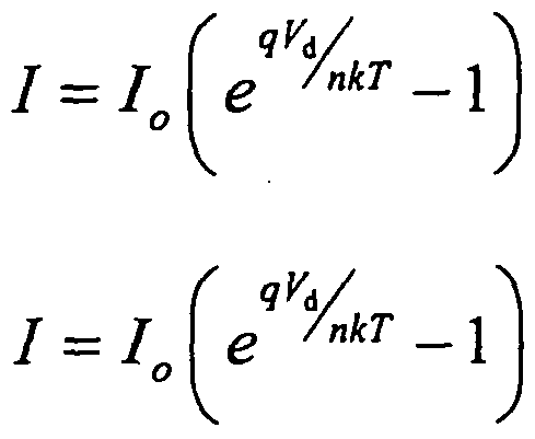
Where I0 is the diode's saturation current, Vd is the diode voltage, n is the diode ideality, k is Boltzman's constant and T is the Temperature. Depending on the local environment, processing conditions, etc., the saturation current can vary significantly from diode to diode. To account for practical issues, the Shockley equation can be alternately expressed:

Where r^ is the diode ideality for the specific diode and the parameter R0A is its resistance- area product at zero volts of applied bias, expressed in units of ohm-cm2. While diode resistance and saturation current depend on area, the R0A product fora specific technology is independent of area and characterizes the quality of diode fabrication.
Different applications of an imaging sensor pixel array may require differing degrees of image quality. For instance, a CMOS sensor used in a studio broadcast camera to generate content for HDTV production (high-end application) requires significantly higher image quality than a CMOS sensor used in consumer camcorders (medium to low-end product application). In addition to the well known attributes such as sensitivity and low noise, other quality factors include drift-free operation and insensitivity to excess illumination. Maximizing image quality hence entails not only better clear pixel quality, but also better OB quality. Consequently, a critical property of an OB pixel (active or dummy) is how closely it truly represents the dark signal response of a clear pixel regardless of incident lighting and environment including physical and electrical stress. For instance, high end applications require an OB pixel to have significantly higher fidelity under extreme conditions, e.g., superior opacity, thermal stability, and well-behaved electrical characteristics including detector ideality, rid, and R0A product. In addition to the difficulty in achieving the necessary opacity in OB pixels without perturbing electrical characteristics, there is also a need for forming dummy pixels that generate the same nominal current as OB pixels and clear pixels. The total current in clear, dummy and an OB pixel is the sum of each diode's Shockley-Read current, photocurrent and the electrical bias current; it is expressed as the direct sum:
/ total = x T - xT photo 4 ~-U D .
where R0 is the detector's resistance at the applied bias, Vd. The total current accumulated in clear pixels versus that in OB pixels should differ only by the clear pixel photocurrent, IPhOto; Iphoto must be zero in OB and OB dummy pixels.
SUMMARY OF THE INVENTION
In general, dummy pixels are disclosed that exhibit identical electrical characteristics to any other pixel in the imaging array. This insures that the total current of each dummy pixel used in an array also containing clear pixels and OB pixels is roughly identical to the total current of a clear pixel. While an OB pixel used as a reference for signal processing is read each frame, a dummy pixel must look the same even though it may never be read, regardless whether it is opaque or light- sensitive. Further, the dummy pixels do not perturb the electrical characteristics of nearby pixels so that they can be used to isolate the various sub-arrays that compose an imaging array. Such dummy pixels are also placed at the edges of the imaging array to prevent discontinuities stemming from process-related, physical and electrical factors. Edge effects are thereby eliminated.
The preferred embodiment of the dummy pixel is a clear type with identical electrical characteristics to the clear pixels in the main imaging array. A second embodiment of the dummy pixel is optically black to support optional signal processing functions.
Dummy OB pixels are constituted in the present invention by: 1) forming the pixels within a standard production process wherein the light- blocking property of the OB pixel is formed separately from basic diode formation including the various annealing steps that mitigate implant damage. An improved method for forming an Optical Black layer separately from the underlying CMOS sensor process is disclosed in U.S. Patent Application Serial No. 1 1/461,457, entitled IMAGE SENSOR AND METHOD FOR MANUFACTURING THE SAME, filed August 1, 2006, the disclosure of which is herein incorporated by reference in its entirety
2) partitioning the pixel array into sub-arrays of clear pixels, dummy pixels, and OB pixels that may be isolated from supporting peripheral circuits by N- guard band regions. The latter guard band regions collect stray minority carriers and prevent extraneous minority carriers from offsetting the OB reference signal. Such guard bands are used in areas adjacent to, for example, high speed digital circuits that emit light as a by-product of hot carrier effects.
In addition to these two steps, dummy OB pixel formation is completed by operating the dummy pixels with the reset transistor biased in soft reset mode to prevent signal integration. This insures low-noise operation and minimizes generation of excess generation-recombination currents that alter diode ideality and/or R0A product.
Dummy clear pixel formation is completed by omitting step 1 and again operating these pixels with the reset transistor biased in soft reset mode. Dummy clear pixels are the main guard bands protecting the imaging array from deleterious edge effects since the omission of the OB step results in the best possible electrical match to the clear pixels in the imaging array.
Thus, in one embodiment, a dummy pixel may comprise a photodiode and a reset transistor connected to the photodiode, wherein the reset transistor is biased in a soft reset mode. A method of the present invention may comprise forming at least one row or column of dummy pixels in an image sensor, wherein each dummy pixel comprises a pixel having a reset transistor permanently biased in a soft reset mode.
An image sensor formed according to the present invention may comprise an array of clear pixels, a plurality of sub-arrays of optical black pixels, and a plurality of sub-arrays of dummy pixels located between the array of clear pixels and the sub-
arrays of optical black pixels, wherein each dummy pixel comprises a photodiode, and a reset transistor connected to the photodiode, wherein the reset transistor is biased in a soft reset mode.
A dummy pixel may be formed as either a clear pixel or an optical black pixel.
BRIEF DESCRIPTION OF THE DRAWINGS
The present invention will be readily understood by the following detailed description in conjunction with the accompanying drawings, wherein like reference numerals designate like structural elements, and in which: Fig. 1 is a cross-section diagram illustrating Ti/TiN Optical Black pixel structure used in OB and dummy pixels;
Fig. 2 is a floor plan of a pixel array wherein the total array is divided into a main image sensor array of Clear Pixels, several subarrays of Optical Black pixels, streets of dummy pixels that separate the clear and OB arrays, and a final N- guard band at one edge;
Fig. 3 A is a schematic of a standard Clear Pixel of the Prior Art; Fig. 3B is schematic of a standard Dummy Pixel of the Prior Art; Fig. 4 is a graph of Optical Black pixel spectral response for different OB technologies, including an embodiment of the present invention; Fig. 5 A is a top-view illustration of an embodiment of the dummy OB pixel structure of the present invention;
Fig. 5B is a side-view illustration of an embodiment of the dummy OB pixel structure of the present invention; and
Fig, 6 is a schematic comparing a clear pixel to the dummy pixel of the present invention.
DFTATLED DESCRIPTION OF THE INVENTION
The following description is provided to enable any person skilled in the art to make and use the invention and sets forth the best modes contemplated by the inventor for carrying out the invention. Various modifications, however, will remain readily apparent to those skilled in the art. Any and all such modifications, equivalents and alternatives are intended to fall within the spirit and scope of the present invention.
In general, the present invention provides clear dummy pixels and Optical Black (OB) dummy pixels having virtually identical electrical characteristics as the clear pixels in the imaging sensor. The dummy pixels are not necessarily read out but form isolation regions within the array that do not create regional discontinuities resulting in edge effects. The dummy pixels are free of the impediments of existing techniques that complicate sensor design and production. Specifically, the Shockley currents generated in the dummy pixels of the various embodiments are approximately identical to the Shockley current of clear pixels. Furthermore, since there is effectively zero photocurrent generated in the dummy OB pixel, the specific photocurrent generated in each clear pixel represents the net signal relative to the black level. Existing techniques generally require significant changes to process technologies and these deviations are incompatible with standard wafer production. The present invention minimizes dispersion in the key photodetector characteristics rid and R0A in order to maximize imaging array uniformity (by minimizing edge effects) and to thereby maximize image quality produced by the imaging sensor. In other words, the idealities and R0A products for clear and OB pixels should be roughly identical and consistent with the generic diode formation technology regardless of the pixel's location and function. Thus, according to the present invention, dummy pixels are clear pixels
which do not have to be read out, but are biased in an alternative configuration that enables attainment of intrinsic performance regardless of pixel location. The clear dummy pixels are used to isolate regions of clear active pixels from OB pixels without inducing edge effects. OB dummy pixels are alternately used for isolation and signal processing operations.
According to an embodiment of the present invention, fabrication of dummy pixels is effectively partitioned into two principal areas: 1) electrical performance and 2) optical performance. By addressing each area in a step by step manner, image sensor electrical performance is unaffected by the additional processing needed to optimally form OB pixels, apply color filters, form microlenses, apply a protecting layer over the sensor surface, and actually operate the various pixels.
An improved method for forming an Optical Black layer separately from the underlying CMOS sensor process is disclosed in U.S. Patent Application Serial No. 11/461,457, entitled IMAGE SENSOR AND METHOD FOR MANUFACTURING THE SAME, filed August 1 , 2006, the disclosure of which is herein incorporated by reference in its entirety. This application describes a method of forming the Optical Black layer by depositing a Ti/TiN layer over the top of the sensor passivation surface and immediately below the Color Filter Planarization layer (sees cross-sectional drawing in Fig. 1). The thickness of the metal mask used for OB formation to render the OB pixel opaque can be adjusted to increase opacity and decrease light transmission into the OB pixel, but is typically on the order of 1000 A when applied via standard sputtering means. By depositing the Ti/TiN layer over the sensor after the bulk of the critical steps are completed, basic pixel performance is separately optimized from OB performance with respect to opacity. In other words, pixel performance is optimized separately from the steps needed to optimize the properties of the optical black, color filters and microlenses.
Light transmission is rendered negligible by using the Ti/TiN overlayer as shown in the transmission plot of Fig.4. While the overlayer blocks incident light from reaching the photodiode, it does not occlude the entire pixel area to enable annealing ions to diffuse through the sensor overlayers to the photodiode. Fig. 5 A shows a top layer view of the
5 pixel layout including the location of the Ti/TiN pad over the photodiode and under the microlens. Fig. 5B is a cross-section plan showing how the Ti/TiN metallization blocks light focused by the microlens, yet allows the photodiode diffusion to be accessible to annealing ions during the final processing steps. The optical black pixel structure of Fig. 5 is further described in related U.S. Patent Application No. TBD, entitled APPARATUS o AND METHOD FOR FORMING OPTICAL BLACK PIXELS WITH UNIFORMLY LOW DARK CURRENT, the disclosure of which is herein incorporated by reference.
In addition to the separately formed Ti/TiN layer, the pixel array of U.S. Serial No. 11/461 ,457 is segmented into isolated sub-array blocks, as illustrated in Fig. 2. The primary blocks include: 5 1. a physically isolated Clear Pixel array within the overall structure
2. clear dummy array regions that separate the Clear Pixel array from the supporting OB sub-array regions.
3. OB dummy array regions that may be optionally included in the dummy sub-arrays 0 4. optional guard band region comprising multiple N- diffusions that are heavily (3V) reverse biased to absorb excess minority carriers adjacent to areas of sensor self-emission during operation.
The clear dummy sub-arrays of Fig. 2 interconnect throughout the array and generally fill the physical space between the clear pixel array and the OB sub-arrays. Dummy arrays are also placed at the very edge of the array except when an optional
n- guard band is used. The latter guard band is typically about 40 to 60 pixels wide, assuming pixel spacing of about 2μm, as a collecting guard band of at least lOOμm width is needed to capture stray minority carriers that may be self-photogenerated or have been scattered or migrated from the clear pixel array or the peripheral circuits surrounding the entire pixel array. Fig. 2 shows an N- guard band located on the right side as it is assumed here that light-emitting digital circuits are present to the right of the pixel array. The N- guard band is composed of a series of diffusions formed with the same sensor implant and diffusion area as the clear pixels to also prevent creation of edge effects while forming an effective sink for stray minority carriers. The schematic circuits of prior art clear pixels and dummy pixels are compared in
Fig. 3. Previously, each dummy pixel photodiode was kept at OV potential by physically connecting the Select signal (SLCT) to the photodiode diffusion and imposing the condition, for dummy pixels, that the SLCT signal be held at OV. Such a bias condition corresponds to full well saturation and is therefore largely unfavorable for attracting large numbers of minority carriers in the typical p-type substrate (electron).
Consequently, while this type guard band can capture a few stray photo-generated signals from the underlying bulk, it can not minimize dark current accumulation in the neighboring pixels. Most importantly, holding dummy pixels at OV resulted in excess generation-recombination current compared to active pixels. Pixels located at the periphery of the pixel array in imaging sensors, i.e., at the outside edges of the pixel structure, typically show an anomalous behavior that is often referred to as edge effect. For example, pixel dark current is often higher along the sensor perimeter. Hence, pixels belonging to, or in proximity of, the pixel array edges normally can not be used as imaging or OB pixels. To reduce the drawback of having imaging pixels too close to the pixel array edges, a certain number of clear
pixels can be used as a buffering region. However, this approach results in a wasted silicon real estate and ultimately in higher product cost.
Significant improvement in minimizing edge effects in the horizontal direction is achieved by using an improved type of dummy pixel. A key point is to devise the dummy pixel configuration so that it helps stabilize the local environment while deflecting minority carriers away from the edges of the pixel array and operating at a quiescent bias that best mimics clear pixels. Another key point is that the dummy pixel is not encumbered with optical black to further insure that its properties are virtually identical to those of clear pixels in the imaging array. The present invention includes a preferred embodiment of this isolation strategy.
As shown in Fig. 6, the dummy pixel consists of a clear pixel that is configured with the reset transistor biased in soft reset mode. Those skilled in the art will appreciate that such a photodiode dynamically pulls minority carriers that are within one diffusion length toward this higher potential (Vaa-Vth; i.e., one threshold voltage below the analog supply voltage) rather than letting them drift in the substrate. By constantly keeping the dummy photodiodes biased in this very favorable electrical condition, the associated junctions collect the stray electrons (minority carriers) rather than letting them continue to drift and scatter through the substrate. The dummy photodiode of the preferred embodiment thus acts a sink for any stray electrons within a diffusion length of the junction. Consequently, this structure substantially reduces excess dark current generation along the edges of the pixel array and thereby eliminates the edge effect.
Figure 6 further compares the configuration of a clear pixel to that of a dummy pixel. A photodiode 10 is connected to a source of a reset transistor Ml. The gate and drain of the reset transistor Ml are connected to a reset line, which is set to the supply voltage of the circuit. The photodiode 10 diffusion of a dummy pixel is held
in soft reset by biasing reset transistor Ml at just below its threshold voltage so that it is operating in the sub-threshold voltage region. In practical terms, since some amount of dark current will always be discharging the photodiode 10, reset transistor Ml can be considered to be in subthreshold bias. In this regime, the photodiode 10 is never directly connected to the RST node that is otherwise kept at a high potential such as the full analog supply voltage, e.g., 3V. The photodiode 10 is thus operated at a voltage that is one threshold voltage below 3V. This configuration intrinsically decouples the photodiode node from the drain of reset transistor Ml to advantageously decouple power supply noise from the OB photodiodes. This coupling noise would otherwise be injected from the power supply node into the pixel array substrate and result in loss of image quality. Hence the shielding mechanism provided by the reset transistor Ml, by virtue of its being in the sub-threshold region rather than operating as a low impedance is provides a significant improvement.
The dummy pixel circuit further includes an amplifier transistor M2 having a gate connected to the photodiode 10 and a source of the reset transistor Ml. A drain of the amplifier transistor M2 is connected to the reset line. A readout transistor M3 has a drain connected to a source of the amplifier transistor M2, and a source connected to a read bus. A gate of the readout transistor M3 is preferably held at zero volts. Compared to a clear pixel layout, this configuration of dummy pixels requires the removal of a "via" contact that would otherwise connect reset transistor Ml to the metal bus supporting reset across each row of pixels. This via contact is present in the clear pixels. It also requires connecting the gate of the reset transistor Ml to its drain terminal. This connection can be implemented by adding a metal 1 bridge shape to the existing clear pixel layout. Since the OB modifications pose minimum intrusion
to the clear pixel layout, they are perfectly suited in minimizing any impact to the symmetry of the pixel array to enable virtually identical behavior amongst the clear and OB pixels apart from response to light.
By setting operation in this thermal equilibrium condition, the R0A products of the dummy pixels are not degraded from the value set by the production process to match the intrinsic R0A products of the clear pixels. Similarly, the diode idealities of dummy and clear pixels also largely match such that the Shockley currents are effectively identical:
1 r dummy OB _ ~ 7 2 dummy _ ~~ 7 J Clear - ~ nάkT //a J r>^_ , f ' /Ur _γ
/ 1I K onA

Claims
What is claimed is: 1. A dummy pixel comprising: a photodiode; and a reset transistor connected to the photodiode, wherein the reset transistor is biased in a soft reset mode.
2. The dummy pixel of Claim 1 , wherein the reset transistor has a gate and drain connected to a reset line, and wherein the reset line is set to a first predetermined voltage.
3. The dummy pixel of Claim 2, wherein the reset line is not connected to a reset bus.
4. The dummy pixel of Claim 3, further comprising an amplifier transistor having a gate connected to the photodiode and a source of the reset transistor, and a drain connected to the reset line.
5. The dummy pixel of Claim 4, further comprising a readout transistor having a drain connected to a source of the amplifier transistor, and having a gate connected to a second predetermined voltage.
6. The dummy pixel of Claim 5, wherein the first predetermined voltage is a circuit supply voltage.
7. The dummy pixel of Claim 6, wherein the second predetermined voltage is zero volts.
8. The dummy pixel of Claim 1, wherein the photodiode forms a current sink for stray electrons.
9. The dummy pixel of Claim I1 wherein the dummy pixel is formed as a clear pixel.
10. T e ummy p xe o aim , optical black pixel.
11. A method for reducing dark current in an image sensor, the method comprising: forming at least one row or column of dummy pixels in an image sensor; wherein each dummy pixel comprises a pixel having a reset transistor permanently biased in a soft reset mode.
12. The method of Claim 11 , wherein a photodiode in each dummy pixel acts a current sink for stray electrons.
13. The method of Claim 11 , wherein the pixel is formed as a clear pixel.
14. The method of Claim 1 1, wherein the pixel is formed as an optical black pixel.
15. The method of Claim 11 , wherein the at least one row or column of dummy pixels is formed on a perimeter region of the image sensor to reduce edge effect.
16. The method of Claim 1 1 , wherein the at least one row or column of dummy pixels is formed between sub-arrays of the image sensor to isolate the sub- arrays from each other.
17. An image sensor comprising: an array of clear pixels; a plurality of sub-arrays of optical black pixels; and a plurality of sub-arrays of dummy pixels located between the array of clear pixels and the sub-arrays of optical black pixels, wherein each dummy pixel comprises: a photodiode; and a reset transistor connected to the photodiode, wherein the reset transistor is biased in a soft reset mode.
18. The image sensor of Claim 17, wherein the reset transistor has a gate and drain connected to a reset line, and wherein the reset line is set to a first predetermined voltage; and wherein the reset line is not connected to a reset bus.
19. The image sensor of Claim 18, further comprising sub-arrays of dummy pixels located on perimeter of the image sensor to reduce edge effect.
20. The image sensor of Claim 18, wherein the dummy pixels are formed as clear pixels.
21. The image sensor of Claim 18, wherein the dummy pixels are formed as optical black pixels.
Priority Applications (2)
| Application Number | Priority Date | Filing Date | Title |
|---|---|---|---|
| EP08725835.6A EP2118919B1 (en) | 2007-03-07 | 2008-02-20 | Apparatus and method for reducing edge effect in an image sensor |
| JP2009552685A JP5260558B2 (en) | 2007-03-07 | 2008-02-20 | Dummy pixel, dark current reduction method, and image sensor |
Applications Claiming Priority (2)
| Application Number | Priority Date | Filing Date | Title |
|---|---|---|---|
| US11/715,736 | 2007-03-07 | ||
| US11/715,736 US7755679B2 (en) | 2007-03-07 | 2007-03-07 | Apparatus and method for reducing edge effect in an image sensor |
Publications (1)
| Publication Number | Publication Date |
|---|---|
| WO2008108926A1 true WO2008108926A1 (en) | 2008-09-12 |
Family
ID=39738569
Family Applications (1)
| Application Number | Title | Priority Date | Filing Date |
|---|---|---|---|
| PCT/US2008/002242 WO2008108926A1 (en) | 2007-03-07 | 2008-02-20 | Apparatus and method for reducing edge effect in an image sensor |
Country Status (4)
| Country | Link |
|---|---|
| US (1) | US7755679B2 (en) |
| EP (1) | EP2118919B1 (en) |
| JP (1) | JP5260558B2 (en) |
| WO (1) | WO2008108926A1 (en) |
Cited By (53)
| Publication number | Priority date | Publication date | Assignee | Title |
|---|---|---|---|---|
| JP2013526801A (en) * | 2010-05-12 | 2013-06-24 | ペリカン イメージング コーポレイション | Architecture for imager arrays and array cameras |
| US9185276B2 (en) | 2013-11-07 | 2015-11-10 | Pelican Imaging Corporation | Methods of manufacturing array camera modules incorporating independently aligned lens stacks |
| US9210392B2 (en) | 2012-05-01 | 2015-12-08 | Pelican Imaging Coporation | Camera modules patterned with pi filter groups |
| US9214013B2 (en) | 2012-09-14 | 2015-12-15 | Pelican Imaging Corporation | Systems and methods for correcting user identified artifacts in light field images |
| US9235900B2 (en) | 2012-08-21 | 2016-01-12 | Pelican Imaging Corporation | Systems and methods for estimating depth and visibility from a reference viewpoint for pixels in a set of images captured from different viewpoints |
| US9253380B2 (en) | 2013-02-24 | 2016-02-02 | Pelican Imaging Corporation | Thin form factor computational array cameras and modular array cameras |
| US9412206B2 (en) | 2012-02-21 | 2016-08-09 | Pelican Imaging Corporation | Systems and methods for the manipulation of captured light field image data |
| US9426361B2 (en) | 2013-11-26 | 2016-08-23 | Pelican Imaging Corporation | Array camera configurations incorporating multiple constituent array cameras |
| US9485496B2 (en) | 2008-05-20 | 2016-11-01 | Pelican Imaging Corporation | Systems and methods for measuring depth using images captured by a camera array including cameras surrounding a central camera |
| US9497370B2 (en) | 2013-03-15 | 2016-11-15 | Pelican Imaging Corporation | Array camera architecture implementing quantum dot color filters |
| US9497429B2 (en) | 2013-03-15 | 2016-11-15 | Pelican Imaging Corporation | Extended color processing on pelican array cameras |
| US9521319B2 (en) | 2014-06-18 | 2016-12-13 | Pelican Imaging Corporation | Array cameras and array camera modules including spectral filters disposed outside of a constituent image sensor |
| US9521416B1 (en) | 2013-03-11 | 2016-12-13 | Kip Peli P1 Lp | Systems and methods for image data compression |
| US9578259B2 (en) | 2013-03-14 | 2017-02-21 | Fotonation Cayman Limited | Systems and methods for reducing motion blur in images or video in ultra low light with array cameras |
| US9733486B2 (en) | 2013-03-13 | 2017-08-15 | Fotonation Cayman Limited | Systems and methods for controlling aliasing in images captured by an array camera for use in super-resolution processing |
| US9741118B2 (en) | 2013-03-13 | 2017-08-22 | Fotonation Cayman Limited | System and methods for calibration of an array camera |
| US9749568B2 (en) | 2012-11-13 | 2017-08-29 | Fotonation Cayman Limited | Systems and methods for array camera focal plane control |
| US9749547B2 (en) | 2008-05-20 | 2017-08-29 | Fotonation Cayman Limited | Capturing and processing of images using camera array incorperating Bayer cameras having different fields of view |
| US9766380B2 (en) | 2012-06-30 | 2017-09-19 | Fotonation Cayman Limited | Systems and methods for manufacturing camera modules using active alignment of lens stack arrays and sensors |
| US9774789B2 (en) | 2013-03-08 | 2017-09-26 | Fotonation Cayman Limited | Systems and methods for high dynamic range imaging using array cameras |
| US9794476B2 (en) | 2011-09-19 | 2017-10-17 | Fotonation Cayman Limited | Systems and methods for controlling aliasing in images captured by an array camera for use in super resolution processing using pixel apertures |
| US9800856B2 (en) | 2013-03-13 | 2017-10-24 | Fotonation Cayman Limited | Systems and methods for synthesizing images from image data captured by an array camera using restricted depth of field depth maps in which depth estimation precision varies |
| US9800859B2 (en) | 2013-03-15 | 2017-10-24 | Fotonation Cayman Limited | Systems and methods for estimating depth using stereo array cameras |
| US9807382B2 (en) | 2012-06-28 | 2017-10-31 | Fotonation Cayman Limited | Systems and methods for detecting defective camera arrays and optic arrays |
| US9813616B2 (en) | 2012-08-23 | 2017-11-07 | Fotonation Cayman Limited | Feature based high resolution motion estimation from low resolution images captured using an array source |
| US9811753B2 (en) | 2011-09-28 | 2017-11-07 | Fotonation Cayman Limited | Systems and methods for encoding light field image files |
| US9866739B2 (en) | 2011-05-11 | 2018-01-09 | Fotonation Cayman Limited | Systems and methods for transmitting and receiving array camera image data |
| US9888194B2 (en) | 2013-03-13 | 2018-02-06 | Fotonation Cayman Limited | Array camera architecture implementing quantum film image sensors |
| US9898856B2 (en) | 2013-09-27 | 2018-02-20 | Fotonation Cayman Limited | Systems and methods for depth-assisted perspective distortion correction |
| US9942474B2 (en) | 2015-04-17 | 2018-04-10 | Fotonation Cayman Limited | Systems and methods for performing high speed video capture and depth estimation using array cameras |
| US9955070B2 (en) | 2013-03-15 | 2018-04-24 | Fotonation Cayman Limited | Systems and methods for synthesizing high resolution images using image deconvolution based on motion and depth information |
| US9986224B2 (en) | 2013-03-10 | 2018-05-29 | Fotonation Cayman Limited | System and methods for calibration of an array camera |
| US10009538B2 (en) | 2013-02-21 | 2018-06-26 | Fotonation Cayman Limited | Systems and methods for generating compressed light field representation data using captured light fields, array geometry, and parallax information |
| US10089740B2 (en) | 2014-03-07 | 2018-10-02 | Fotonation Limited | System and methods for depth regularization and semiautomatic interactive matting using RGB-D images |
| CN108702471A (en) * | 2016-02-29 | 2018-10-23 | 索尼公司 | Solid-state imaging device |
| US10119808B2 (en) | 2013-11-18 | 2018-11-06 | Fotonation Limited | Systems and methods for estimating depth from projected texture using camera arrays |
| US10122993B2 (en) | 2013-03-15 | 2018-11-06 | Fotonation Limited | Autofocus system for a conventional camera that uses depth information from an array camera |
| US10250871B2 (en) | 2014-09-29 | 2019-04-02 | Fotonation Limited | Systems and methods for dynamic calibration of array cameras |
| US10306120B2 (en) | 2009-11-20 | 2019-05-28 | Fotonation Limited | Capturing and processing of images captured by camera arrays incorporating cameras with telephoto and conventional lenses to generate depth maps |
| US10366472B2 (en) | 2010-12-14 | 2019-07-30 | Fotonation Limited | Systems and methods for synthesizing high resolution images using images captured by an array of independently controllable imagers |
| US10390005B2 (en) | 2012-09-28 | 2019-08-20 | Fotonation Limited | Generating images from light fields utilizing virtual viewpoints |
| US10412314B2 (en) | 2013-03-14 | 2019-09-10 | Fotonation Limited | Systems and methods for photometric normalization in array cameras |
| US10482618B2 (en) | 2017-08-21 | 2019-11-19 | Fotonation Limited | Systems and methods for hybrid depth regularization |
| US11270110B2 (en) | 2019-09-17 | 2022-03-08 | Boston Polarimetrics, Inc. | Systems and methods for surface modeling using polarization cues |
| US11290658B1 (en) | 2021-04-15 | 2022-03-29 | Boston Polarimetrics, Inc. | Systems and methods for camera exposure control |
| US11302012B2 (en) | 2019-11-30 | 2022-04-12 | Boston Polarimetrics, Inc. | Systems and methods for transparent object segmentation using polarization cues |
| US11525906B2 (en) | 2019-10-07 | 2022-12-13 | Intrinsic Innovation Llc | Systems and methods for augmentation of sensor systems and imaging systems with polarization |
| US11580667B2 (en) | 2020-01-29 | 2023-02-14 | Intrinsic Innovation Llc | Systems and methods for characterizing object pose detection and measurement systems |
| US11689813B2 (en) | 2021-07-01 | 2023-06-27 | Intrinsic Innovation Llc | Systems and methods for high dynamic range imaging using crossed polarizers |
| US11792538B2 (en) | 2008-05-20 | 2023-10-17 | Adeia Imaging Llc | Capturing and processing of images including occlusions focused on an image sensor by a lens stack array |
| US11797863B2 (en) | 2020-01-30 | 2023-10-24 | Intrinsic Innovation Llc | Systems and methods for synthesizing data for training statistical models on different imaging modalities including polarized images |
| US11954886B2 (en) | 2021-04-15 | 2024-04-09 | Intrinsic Innovation Llc | Systems and methods for six-degree of freedom pose estimation of deformable objects |
| US11953700B2 (en) | 2020-05-27 | 2024-04-09 | Intrinsic Innovation Llc | Multi-aperture polarization optical systems using beam splitters |
Families Citing this family (16)
| Publication number | Priority date | Publication date | Assignee | Title |
|---|---|---|---|---|
| GB2429864B (en) | 2005-09-01 | 2008-09-24 | Micron Technology Inc | Method and apparatus providing pixel array having automatic light control pixels and image capture pixels |
| JP4828547B2 (en) * | 2005-11-02 | 2011-11-30 | シャープ株式会社 | Content data output device, television equipped with the same, and content data output program |
| US7875840B2 (en) * | 2006-11-16 | 2011-01-25 | Aptina Imaging Corporation | Imager device with anti-fuse pixels and recessed color filter array |
| US8077236B2 (en) * | 2008-03-20 | 2011-12-13 | Aptina Imaging Corporation | Method and apparatus providing reduced metal routing in imagers |
| JP5335327B2 (en) | 2008-08-29 | 2013-11-06 | キヤノン株式会社 | Defect detection and correction apparatus and defect detection and correction method |
| US8872953B2 (en) * | 2009-10-30 | 2014-10-28 | Sony Corporation | Solid-state imaging device, manufacturing method thereof, camera, and electronic device |
| JP5735318B2 (en) * | 2011-03-23 | 2015-06-17 | シャープ株式会社 | Solid-state imaging device and electronic information device |
| JP6115982B2 (en) * | 2011-07-04 | 2017-04-19 | ソニーセミコンダクタソリューションズ株式会社 | Imaging device and imaging apparatus |
| US9591242B2 (en) * | 2013-01-31 | 2017-03-07 | Taiwan Semiconductor Manufacturing Company, Ltd. | Black level control for image sensors |
| JP5886793B2 (en) * | 2013-06-11 | 2016-03-16 | 浜松ホトニクス株式会社 | Solid-state imaging device |
| KR102155480B1 (en) | 2014-07-07 | 2020-09-14 | 삼성전자 주식회사 | Image sensor, image processing system including the same, and mobile electronic device including the same |
| WO2016114154A1 (en) * | 2015-01-13 | 2016-07-21 | ソニー株式会社 | Solid-state imaging element, method for manufacturing same, and electronic device |
| JP6515999B2 (en) * | 2015-03-30 | 2019-05-22 | 株式会社ニコン | Imaging device and imaging device |
| JP6887856B2 (en) * | 2017-04-11 | 2021-06-16 | ソニーセミコンダクタソリューションズ株式会社 | Solid-state image sensor |
| EP3595291B1 (en) | 2018-07-11 | 2020-12-30 | IMEC vzw | An image sensor and a method for read-out of pixel signal |
| FR3104814A1 (en) * | 2019-12-11 | 2021-06-18 | Isorg | Image sensor for electronic noise correction of a sensor |
Citations (2)
| Publication number | Priority date | Publication date | Assignee | Title |
|---|---|---|---|---|
| US6777660B1 (en) * | 2002-02-04 | 2004-08-17 | Smal Technologies | CMOS active pixel with reset noise reduction |
| US7172922B2 (en) * | 2002-08-19 | 2007-02-06 | Tower Semiconductor Ltd. | CMOS image sensor array with black pixel using negative-tone resist support layer |
Family Cites Families (14)
| Publication number | Priority date | Publication date | Assignee | Title |
|---|---|---|---|---|
| US4387402A (en) * | 1980-10-28 | 1983-06-07 | Texas Instruments Incorporated | Charge injection imaging device for faithful (dynamic) scene representation |
| JPS6181087A (en) * | 1984-09-28 | 1986-04-24 | Olympus Optical Co Ltd | Solid-state image pickup device |
| JPH05244513A (en) * | 1992-02-26 | 1993-09-21 | Canon Inc | Photoelectric converter and its drive method |
| US6493030B1 (en) * | 1998-04-08 | 2002-12-10 | Pictos Technologies, Inc. | Low-noise active pixel sensor for imaging arrays with global reset |
| US6697111B1 (en) * | 1998-04-08 | 2004-02-24 | Ess Technology, Inc. | Compact low-noise active pixel sensor with progressive row reset |
| KR100284304B1 (en) * | 1998-12-22 | 2001-03-02 | 김영환 | CMOS image sensor and its driving method |
| JP2000196055A (en) * | 1998-12-24 | 2000-07-14 | Toshiba Corp | Solid-state image pickup device |
| US6424375B1 (en) * | 1999-09-21 | 2002-07-23 | Pixel Devices, International | Low noise active reset readout for image sensors |
| JP2001339643A (en) * | 2000-05-30 | 2001-12-07 | Nec Corp | Black level generating circuit for solid-state image pickup device and solid-state image pickup device |
| EP1362475B1 (en) * | 2000-11-16 | 2008-12-10 | California Institute Of Technology | Photodiode cmos imager with column-feedback soft-reset |
| US6911640B1 (en) * | 2002-04-30 | 2005-06-28 | Ess Technology, Inc. | Reducing reset noise in CMOS image sensors |
| JP4242258B2 (en) * | 2003-11-21 | 2009-03-25 | シャープ株式会社 | Solid-state image sensor |
| US7760258B2 (en) * | 2007-03-07 | 2010-07-20 | Altasens, Inc. | Apparatus and method for stabilizing image sensor black level |
| US7999340B2 (en) * | 2007-03-07 | 2011-08-16 | Altasens, Inc. | Apparatus and method for forming optical black pixels with uniformly low dark current |
-
2007
- 2007-03-07 US US11/715,736 patent/US7755679B2/en active Active
-
2008
- 2008-02-20 EP EP08725835.6A patent/EP2118919B1/en active Active
- 2008-02-20 JP JP2009552685A patent/JP5260558B2/en active Active
- 2008-02-20 WO PCT/US2008/002242 patent/WO2008108926A1/en active Application Filing
Patent Citations (2)
| Publication number | Priority date | Publication date | Assignee | Title |
|---|---|---|---|---|
| US6777660B1 (en) * | 2002-02-04 | 2004-08-17 | Smal Technologies | CMOS active pixel with reset noise reduction |
| US7172922B2 (en) * | 2002-08-19 | 2007-02-06 | Tower Semiconductor Ltd. | CMOS image sensor array with black pixel using negative-tone resist support layer |
Non-Patent Citations (1)
| Title |
|---|
| See also references of EP2118919A4 * |
Cited By (114)
| Publication number | Priority date | Publication date | Assignee | Title |
|---|---|---|---|---|
| US11792538B2 (en) | 2008-05-20 | 2023-10-17 | Adeia Imaging Llc | Capturing and processing of images including occlusions focused on an image sensor by a lens stack array |
| US9712759B2 (en) | 2008-05-20 | 2017-07-18 | Fotonation Cayman Limited | Systems and methods for generating depth maps using a camera arrays incorporating monochrome and color cameras |
| US9576369B2 (en) | 2008-05-20 | 2017-02-21 | Fotonation Cayman Limited | Systems and methods for generating depth maps using images captured by camera arrays incorporating cameras having different fields of view |
| US10142560B2 (en) | 2008-05-20 | 2018-11-27 | Fotonation Limited | Capturing and processing of images including occlusions focused on an image sensor by a lens stack array |
| US9749547B2 (en) | 2008-05-20 | 2017-08-29 | Fotonation Cayman Limited | Capturing and processing of images using camera array incorperating Bayer cameras having different fields of view |
| US11412158B2 (en) | 2008-05-20 | 2022-08-09 | Fotonation Limited | Capturing and processing of images including occlusions focused on an image sensor by a lens stack array |
| US10027901B2 (en) | 2008-05-20 | 2018-07-17 | Fotonation Cayman Limited | Systems and methods for generating depth maps using a camera arrays incorporating monochrome and color cameras |
| US9485496B2 (en) | 2008-05-20 | 2016-11-01 | Pelican Imaging Corporation | Systems and methods for measuring depth using images captured by a camera array including cameras surrounding a central camera |
| US10306120B2 (en) | 2009-11-20 | 2019-05-28 | Fotonation Limited | Capturing and processing of images captured by camera arrays incorporating cameras with telephoto and conventional lenses to generate depth maps |
| US9936148B2 (en) | 2010-05-12 | 2018-04-03 | Fotonation Cayman Limited | Imager array interfaces |
| US10455168B2 (en) | 2010-05-12 | 2019-10-22 | Fotonation Limited | Imager array interfaces |
| JP2013526801A (en) * | 2010-05-12 | 2013-06-24 | ペリカン イメージング コーポレイション | Architecture for imager arrays and array cameras |
| US11423513B2 (en) | 2010-12-14 | 2022-08-23 | Fotonation Limited | Systems and methods for synthesizing high resolution images using images captured by an array of independently controllable imagers |
| US10366472B2 (en) | 2010-12-14 | 2019-07-30 | Fotonation Limited | Systems and methods for synthesizing high resolution images using images captured by an array of independently controllable imagers |
| US11875475B2 (en) | 2010-12-14 | 2024-01-16 | Adeia Imaging Llc | Systems and methods for synthesizing high resolution images using images captured by an array of independently controllable imagers |
| US10742861B2 (en) | 2011-05-11 | 2020-08-11 | Fotonation Limited | Systems and methods for transmitting and receiving array camera image data |
| US9866739B2 (en) | 2011-05-11 | 2018-01-09 | Fotonation Cayman Limited | Systems and methods for transmitting and receiving array camera image data |
| US10218889B2 (en) | 2011-05-11 | 2019-02-26 | Fotonation Limited | Systems and methods for transmitting and receiving array camera image data |
| US9794476B2 (en) | 2011-09-19 | 2017-10-17 | Fotonation Cayman Limited | Systems and methods for controlling aliasing in images captured by an array camera for use in super resolution processing using pixel apertures |
| US10375302B2 (en) | 2011-09-19 | 2019-08-06 | Fotonation Limited | Systems and methods for controlling aliasing in images captured by an array camera for use in super resolution processing using pixel apertures |
| US10984276B2 (en) | 2011-09-28 | 2021-04-20 | Fotonation Limited | Systems and methods for encoding image files containing depth maps stored as metadata |
| US9864921B2 (en) | 2011-09-28 | 2018-01-09 | Fotonation Cayman Limited | Systems and methods for encoding image files containing depth maps stored as metadata |
| US10430682B2 (en) | 2011-09-28 | 2019-10-01 | Fotonation Limited | Systems and methods for decoding image files containing depth maps stored as metadata |
| US10275676B2 (en) | 2011-09-28 | 2019-04-30 | Fotonation Limited | Systems and methods for encoding image files containing depth maps stored as metadata |
| US11729365B2 (en) | 2011-09-28 | 2023-08-15 | Adela Imaging LLC | Systems and methods for encoding image files containing depth maps stored as metadata |
| US10019816B2 (en) | 2011-09-28 | 2018-07-10 | Fotonation Cayman Limited | Systems and methods for decoding image files containing depth maps stored as metadata |
| US9811753B2 (en) | 2011-09-28 | 2017-11-07 | Fotonation Cayman Limited | Systems and methods for encoding light field image files |
| US20180197035A1 (en) | 2011-09-28 | 2018-07-12 | Fotonation Cayman Limited | Systems and Methods for Encoding Image Files Containing Depth Maps Stored as Metadata |
| US9754422B2 (en) | 2012-02-21 | 2017-09-05 | Fotonation Cayman Limited | Systems and method for performing depth based image editing |
| US10311649B2 (en) | 2012-02-21 | 2019-06-04 | Fotonation Limited | Systems and method for performing depth based image editing |
| US9412206B2 (en) | 2012-02-21 | 2016-08-09 | Pelican Imaging Corporation | Systems and methods for the manipulation of captured light field image data |
| US9706132B2 (en) | 2012-05-01 | 2017-07-11 | Fotonation Cayman Limited | Camera modules patterned with pi filter groups |
| US9210392B2 (en) | 2012-05-01 | 2015-12-08 | Pelican Imaging Coporation | Camera modules patterned with pi filter groups |
| US9807382B2 (en) | 2012-06-28 | 2017-10-31 | Fotonation Cayman Limited | Systems and methods for detecting defective camera arrays and optic arrays |
| US10334241B2 (en) | 2012-06-28 | 2019-06-25 | Fotonation Limited | Systems and methods for detecting defective camera arrays and optic arrays |
| US10261219B2 (en) | 2012-06-30 | 2019-04-16 | Fotonation Limited | Systems and methods for manufacturing camera modules using active alignment of lens stack arrays and sensors |
| US9766380B2 (en) | 2012-06-30 | 2017-09-19 | Fotonation Cayman Limited | Systems and methods for manufacturing camera modules using active alignment of lens stack arrays and sensors |
| US11022725B2 (en) | 2012-06-30 | 2021-06-01 | Fotonation Limited | Systems and methods for manufacturing camera modules using active alignment of lens stack arrays and sensors |
| US10380752B2 (en) | 2012-08-21 | 2019-08-13 | Fotonation Limited | Systems and methods for estimating depth and visibility from a reference viewpoint for pixels in a set of images captured from different viewpoints |
| US9235900B2 (en) | 2012-08-21 | 2016-01-12 | Pelican Imaging Corporation | Systems and methods for estimating depth and visibility from a reference viewpoint for pixels in a set of images captured from different viewpoints |
| US9858673B2 (en) | 2012-08-21 | 2018-01-02 | Fotonation Cayman Limited | Systems and methods for estimating depth and visibility from a reference viewpoint for pixels in a set of images captured from different viewpoints |
| US9813616B2 (en) | 2012-08-23 | 2017-11-07 | Fotonation Cayman Limited | Feature based high resolution motion estimation from low resolution images captured using an array source |
| US10462362B2 (en) | 2012-08-23 | 2019-10-29 | Fotonation Limited | Feature based high resolution motion estimation from low resolution images captured using an array source |
| US9214013B2 (en) | 2012-09-14 | 2015-12-15 | Pelican Imaging Corporation | Systems and methods for correcting user identified artifacts in light field images |
| US10390005B2 (en) | 2012-09-28 | 2019-08-20 | Fotonation Limited | Generating images from light fields utilizing virtual viewpoints |
| US9749568B2 (en) | 2012-11-13 | 2017-08-29 | Fotonation Cayman Limited | Systems and methods for array camera focal plane control |
| US10009538B2 (en) | 2013-02-21 | 2018-06-26 | Fotonation Cayman Limited | Systems and methods for generating compressed light field representation data using captured light fields, array geometry, and parallax information |
| US9743051B2 (en) | 2013-02-24 | 2017-08-22 | Fotonation Cayman Limited | Thin form factor computational array cameras and modular array cameras |
| US9374512B2 (en) | 2013-02-24 | 2016-06-21 | Pelican Imaging Corporation | Thin form factor computational array cameras and modular array cameras |
| US9253380B2 (en) | 2013-02-24 | 2016-02-02 | Pelican Imaging Corporation | Thin form factor computational array cameras and modular array cameras |
| US9774831B2 (en) | 2013-02-24 | 2017-09-26 | Fotonation Cayman Limited | Thin form factor computational array cameras and modular array cameras |
| US9917998B2 (en) | 2013-03-08 | 2018-03-13 | Fotonation Cayman Limited | Systems and methods for measuring scene information while capturing images using array cameras |
| US9774789B2 (en) | 2013-03-08 | 2017-09-26 | Fotonation Cayman Limited | Systems and methods for high dynamic range imaging using array cameras |
| US10958892B2 (en) | 2013-03-10 | 2021-03-23 | Fotonation Limited | System and methods for calibration of an array camera |
| US9986224B2 (en) | 2013-03-10 | 2018-05-29 | Fotonation Cayman Limited | System and methods for calibration of an array camera |
| US11272161B2 (en) | 2013-03-10 | 2022-03-08 | Fotonation Limited | System and methods for calibration of an array camera |
| US11570423B2 (en) | 2013-03-10 | 2023-01-31 | Adeia Imaging Llc | System and methods for calibration of an array camera |
| US10225543B2 (en) | 2013-03-10 | 2019-03-05 | Fotonation Limited | System and methods for calibration of an array camera |
| US9521416B1 (en) | 2013-03-11 | 2016-12-13 | Kip Peli P1 Lp | Systems and methods for image data compression |
| US9800856B2 (en) | 2013-03-13 | 2017-10-24 | Fotonation Cayman Limited | Systems and methods for synthesizing images from image data captured by an array camera using restricted depth of field depth maps in which depth estimation precision varies |
| US9888194B2 (en) | 2013-03-13 | 2018-02-06 | Fotonation Cayman Limited | Array camera architecture implementing quantum film image sensors |
| US9741118B2 (en) | 2013-03-13 | 2017-08-22 | Fotonation Cayman Limited | System and methods for calibration of an array camera |
| US10127682B2 (en) | 2013-03-13 | 2018-11-13 | Fotonation Limited | System and methods for calibration of an array camera |
| US9733486B2 (en) | 2013-03-13 | 2017-08-15 | Fotonation Cayman Limited | Systems and methods for controlling aliasing in images captured by an array camera for use in super-resolution processing |
| US10412314B2 (en) | 2013-03-14 | 2019-09-10 | Fotonation Limited | Systems and methods for photometric normalization in array cameras |
| US10547772B2 (en) | 2013-03-14 | 2020-01-28 | Fotonation Limited | Systems and methods for reducing motion blur in images or video in ultra low light with array cameras |
| US9578259B2 (en) | 2013-03-14 | 2017-02-21 | Fotonation Cayman Limited | Systems and methods for reducing motion blur in images or video in ultra low light with array cameras |
| US10091405B2 (en) | 2013-03-14 | 2018-10-02 | Fotonation Cayman Limited | Systems and methods for reducing motion blur in images or video in ultra low light with array cameras |
| US9497370B2 (en) | 2013-03-15 | 2016-11-15 | Pelican Imaging Corporation | Array camera architecture implementing quantum dot color filters |
| US10542208B2 (en) | 2013-03-15 | 2020-01-21 | Fotonation Limited | Systems and methods for synthesizing high resolution images using image deconvolution based on motion and depth information |
| US9497429B2 (en) | 2013-03-15 | 2016-11-15 | Pelican Imaging Corporation | Extended color processing on pelican array cameras |
| US10182216B2 (en) | 2013-03-15 | 2019-01-15 | Fotonation Limited | Extended color processing on pelican array cameras |
| US10674138B2 (en) | 2013-03-15 | 2020-06-02 | Fotonation Limited | Autofocus system for a conventional camera that uses depth information from an array camera |
| US10455218B2 (en) | 2013-03-15 | 2019-10-22 | Fotonation Limited | Systems and methods for estimating depth using stereo array cameras |
| US10638099B2 (en) | 2013-03-15 | 2020-04-28 | Fotonation Limited | Extended color processing on pelican array cameras |
| US9800859B2 (en) | 2013-03-15 | 2017-10-24 | Fotonation Cayman Limited | Systems and methods for estimating depth using stereo array cameras |
| US10122993B2 (en) | 2013-03-15 | 2018-11-06 | Fotonation Limited | Autofocus system for a conventional camera that uses depth information from an array camera |
| US9955070B2 (en) | 2013-03-15 | 2018-04-24 | Fotonation Cayman Limited | Systems and methods for synthesizing high resolution images using image deconvolution based on motion and depth information |
| US10540806B2 (en) | 2013-09-27 | 2020-01-21 | Fotonation Limited | Systems and methods for depth-assisted perspective distortion correction |
| US9898856B2 (en) | 2013-09-27 | 2018-02-20 | Fotonation Cayman Limited | Systems and methods for depth-assisted perspective distortion correction |
| US9924092B2 (en) | 2013-11-07 | 2018-03-20 | Fotonation Cayman Limited | Array cameras incorporating independently aligned lens stacks |
| US9185276B2 (en) | 2013-11-07 | 2015-11-10 | Pelican Imaging Corporation | Methods of manufacturing array camera modules incorporating independently aligned lens stacks |
| US10119808B2 (en) | 2013-11-18 | 2018-11-06 | Fotonation Limited | Systems and methods for estimating depth from projected texture using camera arrays |
| US11486698B2 (en) | 2013-11-18 | 2022-11-01 | Fotonation Limited | Systems and methods for estimating depth from projected texture using camera arrays |
| US10767981B2 (en) | 2013-11-18 | 2020-09-08 | Fotonation Limited | Systems and methods for estimating depth from projected texture using camera arrays |
| US9813617B2 (en) | 2013-11-26 | 2017-11-07 | Fotonation Cayman Limited | Array camera configurations incorporating constituent array cameras and constituent cameras |
| US9426361B2 (en) | 2013-11-26 | 2016-08-23 | Pelican Imaging Corporation | Array camera configurations incorporating multiple constituent array cameras |
| US10708492B2 (en) | 2013-11-26 | 2020-07-07 | Fotonation Limited | Array camera configurations incorporating constituent array cameras and constituent cameras |
| US10089740B2 (en) | 2014-03-07 | 2018-10-02 | Fotonation Limited | System and methods for depth regularization and semiautomatic interactive matting using RGB-D images |
| US10574905B2 (en) | 2014-03-07 | 2020-02-25 | Fotonation Limited | System and methods for depth regularization and semiautomatic interactive matting using RGB-D images |
| US9521319B2 (en) | 2014-06-18 | 2016-12-13 | Pelican Imaging Corporation | Array cameras and array camera modules including spectral filters disposed outside of a constituent image sensor |
| US10250871B2 (en) | 2014-09-29 | 2019-04-02 | Fotonation Limited | Systems and methods for dynamic calibration of array cameras |
| US11546576B2 (en) | 2014-09-29 | 2023-01-03 | Adeia Imaging Llc | Systems and methods for dynamic calibration of array cameras |
| US9942474B2 (en) | 2015-04-17 | 2018-04-10 | Fotonation Cayman Limited | Systems and methods for performing high speed video capture and depth estimation using array cameras |
| CN108702471A (en) * | 2016-02-29 | 2018-10-23 | 索尼公司 | Solid-state imaging device |
| EP3425900A4 (en) * | 2016-02-29 | 2019-05-08 | Sony Corporation | Solid-state imaging element |
| US11437418B2 (en) | 2016-02-29 | 2022-09-06 | Sony Corporation | Solid-state image pickup device |
| CN113923387A (en) * | 2016-02-29 | 2022-01-11 | 索尼公司 | Solid-state image pickup device |
| CN108702471B (en) * | 2016-02-29 | 2021-10-22 | 索尼公司 | Solid-state image pickup device |
| US10818026B2 (en) | 2017-08-21 | 2020-10-27 | Fotonation Limited | Systems and methods for hybrid depth regularization |
| US10482618B2 (en) | 2017-08-21 | 2019-11-19 | Fotonation Limited | Systems and methods for hybrid depth regularization |
| US11562498B2 (en) | 2017-08-21 | 2023-01-24 | Adela Imaging LLC | Systems and methods for hybrid depth regularization |
| US11699273B2 (en) | 2019-09-17 | 2023-07-11 | Intrinsic Innovation Llc | Systems and methods for surface modeling using polarization cues |
| US11270110B2 (en) | 2019-09-17 | 2022-03-08 | Boston Polarimetrics, Inc. | Systems and methods for surface modeling using polarization cues |
| US11525906B2 (en) | 2019-10-07 | 2022-12-13 | Intrinsic Innovation Llc | Systems and methods for augmentation of sensor systems and imaging systems with polarization |
| US11842495B2 (en) | 2019-11-30 | 2023-12-12 | Intrinsic Innovation Llc | Systems and methods for transparent object segmentation using polarization cues |
| US11302012B2 (en) | 2019-11-30 | 2022-04-12 | Boston Polarimetrics, Inc. | Systems and methods for transparent object segmentation using polarization cues |
| US11580667B2 (en) | 2020-01-29 | 2023-02-14 | Intrinsic Innovation Llc | Systems and methods for characterizing object pose detection and measurement systems |
| US11797863B2 (en) | 2020-01-30 | 2023-10-24 | Intrinsic Innovation Llc | Systems and methods for synthesizing data for training statistical models on different imaging modalities including polarized images |
| US11953700B2 (en) | 2020-05-27 | 2024-04-09 | Intrinsic Innovation Llc | Multi-aperture polarization optical systems using beam splitters |
| US11683594B2 (en) | 2021-04-15 | 2023-06-20 | Intrinsic Innovation Llc | Systems and methods for camera exposure control |
| US11290658B1 (en) | 2021-04-15 | 2022-03-29 | Boston Polarimetrics, Inc. | Systems and methods for camera exposure control |
| US11954886B2 (en) | 2021-04-15 | 2024-04-09 | Intrinsic Innovation Llc | Systems and methods for six-degree of freedom pose estimation of deformable objects |
| US11689813B2 (en) | 2021-07-01 | 2023-06-27 | Intrinsic Innovation Llc | Systems and methods for high dynamic range imaging using crossed polarizers |
Also Published As
| Publication number | Publication date |
|---|---|
| US20080218608A1 (en) | 2008-09-11 |
| EP2118919A4 (en) | 2014-07-02 |
| US7755679B2 (en) | 2010-07-13 |
| JP2010520708A (en) | 2010-06-10 |
| JP5260558B2 (en) | 2013-08-14 |
| EP2118919B1 (en) | 2016-04-13 |
| EP2118919A1 (en) | 2009-11-18 |
Similar Documents
| Publication | Publication Date | Title |
|---|---|---|
| US7755679B2 (en) | Apparatus and method for reducing edge effect in an image sensor | |
| US9257472B2 (en) | Solid-state imaging device, camera, and design method for solid-state imaging device | |
| US10224362B2 (en) | Solid-state image pickup element and image pickup apparatus | |
| CN107124565B (en) | Image pickup apparatus | |
| US7456880B2 (en) | Photoelectric conversion element having a plurality of semiconductor regions and including conductive layers provided on each isolation element region | |
| JP4649623B2 (en) | Solid-state imaging device and pixel signal reading method thereof | |
| TWI478331B (en) | Backside-illuminated (bsi) image sensor with reduced blooming and electrical shutter | |
| US8411174B2 (en) | Shielding black reference pixels in image sensors | |
| JP5178266B2 (en) | Solid-state imaging device | |
| EP2980852B1 (en) | Solid-state image sensing element and imaging system | |
| TWI541986B (en) | Black reference pixel for backside illuminated image sensor | |
| EP1341377A2 (en) | Signal processing device for image pickup apparatus | |
| US20070069248A1 (en) | Solid-state image pickup device | |
| US7964902B2 (en) | Imaging device | |
| JP2001230400A (en) | Solid-state image sensor | |
| TWI629771B (en) | Solid-state imaging element, method of manufacturing the same, and imaging device | |
| US20140340541A1 (en) | Solid-state imaging apparatus and camera | |
| US7999340B2 (en) | Apparatus and method for forming optical black pixels with uniformly low dark current | |
| JPH05175471A (en) | Solid-state image sensing device | |
| JP7115067B2 (en) | Solid-state imaging device and imaging system |
Legal Events
| Date | Code | Title | Description |
|---|---|---|---|
| 121 | Ep: the epo has been informed by wipo that ep was designated in this application |
Ref document number: 08725835 Country of ref document: EP Kind code of ref document: A1 |
|
| WWE | Wipo information: entry into national phase |
Ref document number: 2009552685 Country of ref document: JP |
|
| NENP | Non-entry into the national phase |
Ref country code: DE |
|
| WWE | Wipo information: entry into national phase |
Ref document number: 2008725835 Country of ref document: EP |