WO2003071346A1 - Display device - Google Patents
Display device Download PDFInfo
- Publication number
- WO2003071346A1 WO2003071346A1 PCT/IB2003/000196 IB0300196W WO03071346A1 WO 2003071346 A1 WO2003071346 A1 WO 2003071346A1 IB 0300196 W IB0300196 W IB 0300196W WO 03071346 A1 WO03071346 A1 WO 03071346A1
- Authority
- WO
- WIPO (PCT)
- Prior art keywords
- fluid
- display device
- layer
- support plate
- state
- Prior art date
Links
Classifications
-
- G—PHYSICS
- G02—OPTICS
- G02F—OPTICAL DEVICES OR ARRANGEMENTS FOR THE CONTROL OF LIGHT BY MODIFICATION OF THE OPTICAL PROPERTIES OF THE MEDIA OF THE ELEMENTS INVOLVED THEREIN; NON-LINEAR OPTICS; FREQUENCY-CHANGING OF LIGHT; OPTICAL LOGIC ELEMENTS; OPTICAL ANALOGUE/DIGITAL CONVERTERS
- G02F1/00—Devices or arrangements for the control of the intensity, colour, phase, polarisation or direction of light arriving from an independent light source, e.g. switching, gating or modulating; Non-linear optics
- G02F1/01—Devices or arrangements for the control of the intensity, colour, phase, polarisation or direction of light arriving from an independent light source, e.g. switching, gating or modulating; Non-linear optics for the control of the intensity, phase, polarisation or colour
- G02F1/165—Devices or arrangements for the control of the intensity, colour, phase, polarisation or direction of light arriving from an independent light source, e.g. switching, gating or modulating; Non-linear optics for the control of the intensity, phase, polarisation or colour based on translational movement of particles in a fluid under the influence of an applied field
- G02F1/166—Devices or arrangements for the control of the intensity, colour, phase, polarisation or direction of light arriving from an independent light source, e.g. switching, gating or modulating; Non-linear optics for the control of the intensity, phase, polarisation or colour based on translational movement of particles in a fluid under the influence of an applied field characterised by the electro-optical or magneto-optical effect
- G02F1/167—Devices or arrangements for the control of the intensity, colour, phase, polarisation or direction of light arriving from an independent light source, e.g. switching, gating or modulating; Non-linear optics for the control of the intensity, phase, polarisation or colour based on translational movement of particles in a fluid under the influence of an applied field characterised by the electro-optical or magneto-optical effect by electrophoresis
-
- G—PHYSICS
- G02—OPTICS
- G02B—OPTICAL ELEMENTS, SYSTEMS OR APPARATUS
- G02B26/00—Optical devices or arrangements for the control of light using movable or deformable optical elements
- G02B26/004—Optical devices or arrangements for the control of light using movable or deformable optical elements based on a displacement or a deformation of a fluid
- G02B26/005—Optical devices or arrangements for the control of light using movable or deformable optical elements based on a displacement or a deformation of a fluid based on electrowetting
-
- G—PHYSICS
- G02—OPTICS
- G02F—OPTICAL DEVICES OR ARRANGEMENTS FOR THE CONTROL OF LIGHT BY MODIFICATION OF THE OPTICAL PROPERTIES OF THE MEDIA OF THE ELEMENTS INVOLVED THEREIN; NON-LINEAR OPTICS; FREQUENCY-CHANGING OF LIGHT; OPTICAL LOGIC ELEMENTS; OPTICAL ANALOGUE/DIGITAL CONVERTERS
- G02F1/00—Devices or arrangements for the control of the intensity, colour, phase, polarisation or direction of light arriving from an independent light source, e.g. switching, gating or modulating; Non-linear optics
- G02F1/01—Devices or arrangements for the control of the intensity, colour, phase, polarisation or direction of light arriving from an independent light source, e.g. switching, gating or modulating; Non-linear optics for the control of the intensity, phase, polarisation or colour
- G02F1/17—Devices or arrangements for the control of the intensity, colour, phase, polarisation or direction of light arriving from an independent light source, e.g. switching, gating or modulating; Non-linear optics for the control of the intensity, phase, polarisation or colour based on variable-absorption elements not provided for in groups G02F1/015 - G02F1/169
-
- G—PHYSICS
- G09—EDUCATION; CRYPTOGRAPHY; DISPLAY; ADVERTISING; SEALS
- G09F—DISPLAYING; ADVERTISING; SIGNS; LABELS OR NAME-PLATES; SEALS
- G09F9/00—Indicating arrangements for variable information in which the information is built-up on a support by selection or combination of individual elements
- G09F9/30—Indicating arrangements for variable information in which the information is built-up on a support by selection or combination of individual elements in which the desired character or characters are formed by combining individual elements
- G09F9/37—Indicating arrangements for variable information in which the information is built-up on a support by selection or combination of individual elements in which the desired character or characters are formed by combining individual elements being movable elements
- G09F9/372—Indicating arrangements for variable information in which the information is built-up on a support by selection or combination of individual elements in which the desired character or characters are formed by combining individual elements being movable elements the positions of the elements being controlled by the application of an electric field
-
- G—PHYSICS
- G02—OPTICS
- G02B—OPTICAL ELEMENTS, SYSTEMS OR APPARATUS
- G02B2207/00—Coding scheme for general features or characteristics of optical elements and systems of subclass G02B, but not including elements and systems which would be classified in G02B6/00 and subgroups
- G02B2207/115—Electrowetting
-
- G—PHYSICS
- G02—OPTICS
- G02F—OPTICAL DEVICES OR ARRANGEMENTS FOR THE CONTROL OF LIGHT BY MODIFICATION OF THE OPTICAL PROPERTIES OF THE MEDIA OF THE ELEMENTS INVOLVED THEREIN; NON-LINEAR OPTICS; FREQUENCY-CHANGING OF LIGHT; OPTICAL LOGIC ELEMENTS; OPTICAL ANALOGUE/DIGITAL CONVERTERS
- G02F1/00—Devices or arrangements for the control of the intensity, colour, phase, polarisation or direction of light arriving from an independent light source, e.g. switching, gating or modulating; Non-linear optics
- G02F1/01—Devices or arrangements for the control of the intensity, colour, phase, polarisation or direction of light arriving from an independent light source, e.g. switching, gating or modulating; Non-linear optics for the control of the intensity, phase, polarisation or colour
- G02F1/165—Devices or arrangements for the control of the intensity, colour, phase, polarisation or direction of light arriving from an independent light source, e.g. switching, gating or modulating; Non-linear optics for the control of the intensity, phase, polarisation or colour based on translational movement of particles in a fluid under the influence of an applied field
- G02F1/1675—Constructional details
- G02F2001/1678—Constructional details characterised by the composition or particle type
Definitions
- the invention relates to a display device comprising picture elements having at least one first fluid and a second fluid immiscible with each other within a space between a first support plate and a second support plate, one of the fluids being electroconductive or polar, the device comprising means for creating at least two different states.
- the invention further relates to a switchable diffusing device.
- Display devices like TFT-LCDs are used in laptop computers and in organizers, but also find an increasingly wider application in GSM telephones. Instead of LCDs, for example, (polymer) LED display devices are also being used.
- the diffusing device may be used in several devices such as cameras.
- the display device has at least two different states, in which one of the fluids in a first state adjoins at least the first support plate and in the second state the other fluid at least partly adjoins the first support plate.
- the invention is based on a principle discovered by the inventors so called layer break up, but on the other hand layer displacement may be used.
- the invention provides new ways of using these principles.
- a two layer system which comprises a water layer on top of the oil layer.
- the oil layer breaks up due to electrostatic forces. Since parts of the water now penetrate the oil layer the picture element becomes partly transparent.
- the contrast is limited by the fraction of area occupied by the droplets of the (first) fluid ((colored) oil) remaining after the break-up. Typically, depending on the thickness of the original fluid layer an area of 25 - 50 % is realized. This can be decreased further by applying higher voltages, which however would increase the dissipated power significantly. Ideally, one would like the remnant area occupied by the fluid, in this case optically absorbing oil, to approach 0%.
- a further limitation is that, upon break-up, the area fraction is reduced instantly to about 50%. It is therefore hard to obtain area fractions close to 100 %. As a result realizing of analog gray scales may become difficult.
- a picture element corresponds to a defined space (e.g. a substantially closed space) and in the second state the other fluid substantially completely adjoins the first support plate.
- a defined space e.g. a substantially closed space
- the threshold field for layer break up (or displacement) will be exceeded only at certain specific places. At those places oil-film break up (or displacement) will be initiated.
- An inhomogeneous applied electric field can be obtained in several ways.
- the dielectric layer between an electrode and the surface of the part of the first support plate varies in thickness.
- the dielectric layer between an electrode and the surface of the part of the first support plate has a varying dielectric constant.
- oil-film break up By increasing the electric field the threshold for oil-film break up (or displacement) is displaced over the area of the support plate and can be controlled. This makes possible the realization of grey levels.
- oil-film break up (or displacement) can be controlled by varying the wettability of the part of the first support plate or the thickness of the first fluid layer.
- a picture element corresponds to a defined space and in the first state the other fluid layer substantially completely adjoins both support plates.
- the other fluid layer (the oil layer) is now divided in two sub-layers, which each may be thinner. This makes it possible on the one hand to use lower voltages to make oil- film break up (or displacement) occur. On the other hand this opens the opportunity to color displays and the realizing of a larger variety of gray- values.
- a picture element corresponds to a defined space having a further wall dividing the space into at least two sub- picture elements, in the first state a further other fluid layer adjoining the first support plate at least partly within the sub-picture elements.
- the device preferably comprises means to prevent part of the other fluid layer and the further other fluid layer to intermix in the second state.
- Fig. 1 is a diagrammatic cross-section of a part of a display device according to the invention
- Fig. 2 is another diagrammatic cross-section of a part of a display device according to the invention.
- Fig. 3 is a diagrammatic of a part of a display device according to the invention
- Fig. 4 is a diagrammatic cross-section of a part of a color display device according to the invention, while
- Figures 5, 6 and 7 show further embodiments of the invention and Figure 8 shows another diagrammatic cross-section of a part of a display device according to the invention
- the Figures are diagrammatic and not drawn to scale. Corresponding elements are generally denoted by the same reference numerals.
- Fig. 1 shows a diagrammatic cross-section of a part of a display device 1 according to the invention.
- a first fluid 5 and a second fluid 6 are provided, which are immiscible with each other.
- the first fluid 5 is for instance an alkane like hexadecane or as in this example a (silicone) oil.
- the second fluid 6 is electroconductive or polar, for instance water or a salt solution (e.g. a solution of KC1 in a mixture of water and ethyl alcohol).
- a salt solution e.g. a solution of KC1 in a mixture of water and ethyl alcohol.
- a transparent electrode 7 for example indium (tin) oxide is provided and an intermediate hydrophobic layer 8, in this example an amorphous fluoropolymer (AF1600).
- AF1600 amorphous fluoropolymer
- the inventors have found that when a voltage is applied (voltage source 9) the layer 5 breaks up into small droplets (Fig. lb, fragmented film). Break-up occurs when the electrical energy gain is larger than the surface energy loss due to the creation of curved surfaces. As a very important aspect it was found that reversible switching between a continuous film and a fragmented film is achieved by means of the electrical switching means (voltage source 9).
- This effect can be used for electro - optical effects, especially if a colored oil is used a display effect.
- This is achieved with an optically active oil, for example an opaque or reflective oil.
- a fluid with optically active particles is used or a dye material is dissolved in the oil.
- the electro - optical effect may either be used in a transparent way, by using a back light, as for instance known from LCD technology or in a reflective way by using a (diffusive) reflector.
- the droplet size depends on the voltage applied, which in principle offers the possibility of introducing intermediate transmission (or reflection) states (gray levels).
- the area fraction is reduced practically instantly to about 50%. It is therefore hard to obtain area fractions between 50% and 100 %.
- the contrast is limited by the fraction of area occupied by the droplets resulting after the break-up.
- At practical voltages in view of driving the display with IC drivers) see a minimal area fraction of about 25 % is observed. This can be decreased further by applying higher voltages which, however, would increase the dissipated power significantly and possibly preclude the use of low voltage IC drivers.
- the intermediate hydrophobic layers 8 have a curved form with the smallest thickness in the center, ensuring that the electrical field is highest in the center of a picture element 2.
- the field varies in a radial manner (by the varying thickness of the insulator).
- the threshold field will be first exceeded at the center of the pixel, where the insulator has the minimum thickness.
- the position at which the applied field equals the threshold field will move outward, hence moving the oil to the side of the pixel.
- the schematic drawing in Figure 3 shows a cross-section of a pixel that is either circularly symmetric, or has a rectangular shape.
- the oil will be pushed outward in a ring-like shape, starting from a single point in the center of the pixel.
- a insulator shaped like a slice of cylinder so that the oil break-up will start along a line, and the oil is pushed out in a curtain-like fashion.
- the stray field distribution at the edge of electrodes is used, or a special electrode structure (segmented, perforated) that provides the desired inhomogeneous field distribution is used.
- oil break up has been considered, similar arguments apply to a device base on fluid displacement.
- an inhomogeneous oil layer due to e.g. insufficient volume, thickness variation or contact angles) may initiate the oil displacements (or break up).
- the pixel walls 13 By either fabricating the pixel walls 13 out of a different material than the material of the layers 8, 8' (e.g. Teflon like AF 1600) or providing these walls 13 with such material 14 with a sufficiently high surface energy such that: yH 2 0,S ⁇ ⁇ oil,H 2 0 " * " 7oil,S
- each layer can now be switched independently by contacting the water 6 by means of a through-connection (electrode 12 in Figure 4) through the upper (or lower) AF1600 layer. In practice this can be done by grounding the water 6 by means of electrode 12 and applying a voltage to either electrode 7 or electrode 11.
- the device further comprises a diffuse white reflector 15. The viewing direction is indicated in Figure 4 by the arrows 16.
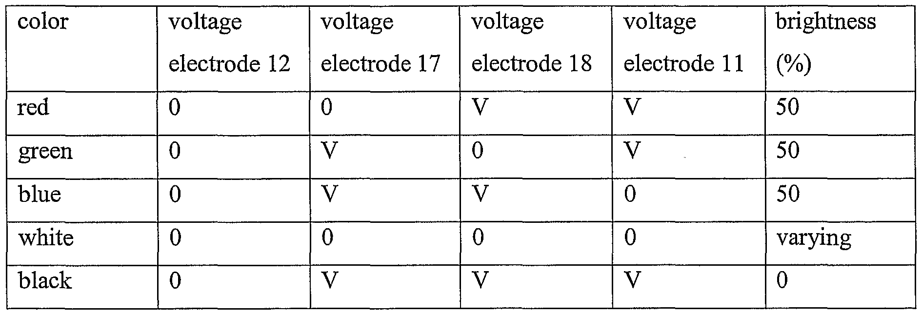
- Example 1 Three color display
- the oils 5 have different colors by using different dyes to realize a color display.
- three kinds of e.g. oil are used, viz a red layer 5R, a green layer 5G and a blue layer 5B, to obtain the highest possible brightness for the configuration shown in Figure 5.
- a single pixel comprises a black absorber 16 (background) and two sub-pixels A and B, each having a configuration comparable to the one shown in Figure 4.
- the oil layer 5B on the top in the first state covers half of each of the sub- pixels. This can be achieved by locally modifying the surface energy of the layer 8' (AF1600).
- the other fluid, in this case water is assumed to be at a fixed voltage, for example ground (0V) via electrode 12.
- electrode 17 underneath the red layer of oil 5R should be grounded (0 V) whereas electrode 18 underneath the green layer of oil 5G and electrode 11 above the blue layer of oil 5B should be activated by applying a voltage V.
- the green and blue layers will break up or move to the side and the sub-pixel B above the black absorber 16 becomes transparent.
- the total pixel will appear red, since sub-pixel A looks red and sub-pixel B looks black.
- the maximum brightness is limited to 50%). This maximum brightness is a significant improvement with respect to a configuration with 3 parallel pixels, where the maximum brightness is limited to 33%.
- Table 1 A summary of the voltages applied to the electrodes and the maximum brightness for each of the primary colors, black and white is given in Table 1.
- the white state is obtained by reflecting light of all colored layers simultaneously.
- the color distribution of the white state depends strongly on the size chosen for the blue layer 5B.
- the blue layer occupies half of the pixel.
- the green and the red will contribute 25 % to the white, which will seem distorted.
- the blue layer covers 33% of the total area, the color distribution of the white state will look better, albeit with a low overall reflectivity of 33%.
- the blue state will reach a maximum brightness of 33 % instead o f 50% .
- the configuration as shown in Figure 5 is chosen as an example. Other configurations, with red or green on top can be used as well. In fact, by choosing the color with the highest reflectivity on top, one can reduce the color distortion caused by the different sizes of the area occupied by each of the colors and/or account for the eye sensitivity.
- Example 2 Three color plus white display
- Example 1 The variation in brightness in the white state arising in Example 1 can be circumvented by using a white oil.
- a white oil is e.g. obtained by dispersing scattering particles in the oil.
- the configuration shown in figure 6 uses such a white oil.
- different colors are obtained by providing voltages to electrodes 17 (underneath the red layers of oil 5R), the electrodes 18 (underneath the green layers of oil 5G), the elecfrodes 19 (above the blue layer of oil 5B) and the elecfrodes 20 (above the white layer of oil 5W).
- Table 2 The result is given in Table 2.
- the color ordering can be altered if necessary.
- a high brightness white state reflecting 100% can be achieved when the black absorber 16 is replaced by a white reflector and the oil layer at the top of sub-pixel B is black.
- no satisfactory black state can be obtained, due to the contribution of sub-pixel A which is either in a colored or a white state. Tins however reduces the contrast obtained.
- Example 3 - Subfractive color display Alternatively as shown in Figure7 subfractive colors may be used. If two oil- layers 5 inside each sub-pixel are used one primary color per sub-pixel can be achieved. If a fixed subfractive color filter 21 is provided on top, a major improvement of the display performance is obtained.
- the pixel shown in Figure 7 consists of three sub-pixels A, B and C. In each of the sub-pixels the order of the subfractive colors alternates, i.e. M(agenta), C(yan), Y(ellow) for sub-pixel A, C(yan), Y(ellow), M(agenta), for sub-pixel B and Y(ellow), M(agenta), C(yan) for sub-pixel C.
- each of the primary colors in at least two of the sub- pixels.
- the magenta color filter part 21M absorbs green and the (switchable) yellow bottom oil layer 5Y absorbs blue.
- the top cyan oil layer 5C which absorbs red is switched to a transparent state, the red light is reflected by the white background layer (reflector 22) and sub-pixel A will appear red.
- sub-pixel C will appear red by switching the bottom oil layer 5C to a transparent state.
- the cyan color filter 21 C absorbs red and if none of the oil layers 5Y, 5M in B are switched to the transparent state will the sub-pixel B will appear black. Since the sub-pixels are sufficiently small the human eye does not distinguish the individual responses and the total pixel will appear red with a maximum brightness of 67%). Other colors can be obtained in a similar fashion.
- Table 3 A summary of the colors and the corresponding voltage states are given in Table 3.
- the protective scope of the invention is not limited to the embodiments described.
- the layer 6 may be chosen to be scattering (by using a solution of TiO 2 ) or reflective (by using a solution of a suitable pigment).
- Driving voltages may also be capacitively coupled to the elecfrodes; especially capacitive coupling to electrodes 12 prevents degradation of the fluid 5.
- One or more reservoirs may be incorporated for overflow or supply of fluid(s) if fluid volumes in the reservoirs change due to temperature, pressure or otherwise.
- Figure 8 finally shows an embodiment in which the pixel walls 13 do not extend across the whole pixel thickness. It appears that the oil film 5 is very stable, which is enhanced even further as the pixel size decreases. So during switching the oil remains confined in each area providing the wall is not less than twice the height of the off-state oil film thickness. This means that a common channel can be employed for the fluid 6, which simplifies display fabrication and driving. The single electrical contact to the liquid can then be made externally.
- the other reference numerals have the same meaning as those in Figure 4.
- the invention resides in each and every novel characteristic feature and each and every combination of characteristic features. Reference numerals in the claims do not limit their protective scope. Use of the verb "to comprise” and its conjugations does not exclude the presence of elements other than those stated in the claims. Use of the article "a” or "an” preceding an element does not exclude the presence of a plurality of such elements.
Abstract
Description


Claims
Priority Applications (11)
| Application Number | Priority Date | Filing Date | Title |
|---|---|---|---|
| KR1020117010095A KR101230710B1 (en) | 2002-02-19 | 2003-01-24 | Display device |
| US10/504,708 US7463398B2 (en) | 2002-02-19 | 2003-01-24 | Display device |
| AT03742617T ATE548678T1 (en) | 2002-02-19 | 2003-01-24 | DISPLAY DEVICE |
| KR10-2004-7012687A KR20040089637A (en) | 2002-02-19 | 2003-01-24 | Display device |
| ES03742617T ES2385017T3 (en) | 2002-02-19 | 2003-01-24 | Display device |
| KR1020117005258A KR101128633B1 (en) | 2002-02-19 | 2003-01-24 | Display device |
| JP2003570180A JP4653398B2 (en) | 2002-02-19 | 2003-01-24 | Display device |
| EP03742617A EP1478974B1 (en) | 2002-02-19 | 2003-01-24 | Display device |
| AU2003201141A AU2003201141A1 (en) | 2002-02-19 | 2003-01-24 | Display device |
| US12/292,015 US7898718B2 (en) | 2002-02-19 | 2008-11-10 | Display device |
| US13/014,292 US8213071B2 (en) | 2002-02-19 | 2011-01-26 | Display device |
Applications Claiming Priority (2)
| Application Number | Priority Date | Filing Date | Title |
|---|---|---|---|
| EP02075676.3 | 2002-02-19 | ||
| EP02075676 | 2002-02-19 |
Related Child Applications (2)
| Application Number | Title | Priority Date | Filing Date |
|---|---|---|---|
| US10504708 A-371-Of-International | 2003-01-24 | ||
| US12/292,015 Continuation US7898718B2 (en) | 2002-02-19 | 2008-11-10 | Display device |
Publications (1)
| Publication Number | Publication Date |
|---|---|
| WO2003071346A1 true WO2003071346A1 (en) | 2003-08-28 |
Family
ID=27741170
Family Applications (1)
| Application Number | Title | Priority Date | Filing Date |
|---|---|---|---|
| PCT/IB2003/000196 WO2003071346A1 (en) | 2002-02-19 | 2003-01-24 | Display device |
Country Status (10)
| Country | Link |
|---|---|
| US (3) | US7463398B2 (en) |
| EP (1) | EP1478974B1 (en) |
| JP (2) | JP4653398B2 (en) |
| KR (4) | KR101230710B1 (en) |
| CN (2) | CN1633622A (en) |
| AT (1) | ATE548678T1 (en) |
| AU (1) | AU2003201141A1 (en) |
| ES (1) | ES2385017T3 (en) |
| TW (1) | TWI288261B (en) |
| WO (1) | WO2003071346A1 (en) |
Cited By (49)
| Publication number | Priority date | Publication date | Assignee | Title |
|---|---|---|---|---|
| WO2004027489A1 (en) * | 2002-09-19 | 2004-04-01 | Koninklijke Philips Electronics N.V. | Switchable optical element |
| WO2004104670A1 (en) | 2003-05-22 | 2004-12-02 | Koninklijke Philips Electronics N.V. | Display device |
| WO2006021912A1 (en) * | 2004-08-26 | 2006-03-02 | Koninklijke Philips Electronics N.V. | Display device based on immiscible fluids |
| WO2005098797A3 (en) * | 2004-04-08 | 2006-04-06 | Koninkl Philips Electronics Nv | Display device |
| EP1671304A1 (en) * | 2003-10-08 | 2006-06-21 | E Ink Corporation | Electro-wetting displays |
| WO2006090317A1 (en) * | 2005-02-28 | 2006-08-31 | Koninklijke Philips Electronics N.V. | Display device |
| JP2007508576A (en) * | 2003-10-08 | 2007-04-05 | コーニンクレッカ フィリップス エレクトロニクス エヌ ヴィ | Electrowetting display device |
| WO2007141219A1 (en) * | 2006-06-06 | 2007-12-13 | Liquavista B.V. | Colour display device |
| WO2008026179A2 (en) * | 2006-08-31 | 2008-03-06 | Koninklijke Philips Electronics N.V. | Electronic device based on electrowetting effect |
| WO2009143074A2 (en) * | 2008-05-18 | 2009-11-26 | Roy Rosser | Photo-sensitive, bistable, electrowetting light valve |
| US7800816B2 (en) | 2004-04-05 | 2010-09-21 | Liquavista B.V. | Display device based on electrowetting effect |
| WO2010133690A1 (en) | 2009-05-20 | 2010-11-25 | Liquavista B.V. | Method of manufacturing an optical display |
| WO2011048424A2 (en) | 2009-10-23 | 2011-04-28 | Plastic Logic Limited | Electronic document reading devices |
| WO2011051413A1 (en) | 2009-10-29 | 2011-05-05 | Liquavista B.V. | Driving an electrowetting display device |
| WO2011058019A1 (en) | 2009-11-10 | 2011-05-19 | Liquavista B.V. | Method for making electrowetting display device |
| WO2011080224A1 (en) | 2009-12-30 | 2011-07-07 | Liquavista B.V. | Electrowetting display device |
| WO2011135044A1 (en) | 2010-04-29 | 2011-11-03 | Samsung Lcd Netherlands R & D Center B.V. | Improvements in relation to a manufacturing method for an electrowetting device |
| WO2011157826A1 (en) | 2010-06-18 | 2011-12-22 | Samsung Lcd Netherlands R & D Center B.V. | An electrowetting element and fluid |
| US8154486B2 (en) | 2007-03-30 | 2012-04-10 | Samsung Lcd Netherlands R&D Center B.V. | Driving of electrowetting display device |
| US8189267B2 (en) | 2008-06-27 | 2012-05-29 | Samsung Lcd Netherlands R&D Center B.V. | Electrowetting display device |
| US8199409B2 (en) | 2007-05-23 | 2012-06-12 | Samsung Lcd Netherlands R&D Center B.V. | Electrowetting elements and optical display devices |
| WO2012126851A1 (en) | 2011-03-21 | 2012-09-27 | Samsung Lcd Netherlands R & D Center B.V. | Dispensing method and device for dispensing |
| WO2012175346A1 (en) | 2011-06-24 | 2012-12-27 | Samsung LCD Netherlands R & D Center B.V | Electrowetting display device |
| US8350783B2 (en) | 2007-05-24 | 2013-01-08 | Samsung Lcd Netherlands R&D Center B.V. | Electrowetting element, display device and control system |
| US8384985B2 (en) | 2007-12-06 | 2013-02-26 | Samsung Lcd Netherlands R & D Center B.V. | Transflective electrowetting display device |
| WO2013026877A1 (en) | 2011-08-24 | 2013-02-28 | Samsung Lcd Netherlands R & D Center B.V. | Electrowetting display device |
| WO2013037982A2 (en) | 2011-09-16 | 2013-03-21 | Samsung Lcd Netherlands R & D Center B.V. | Display device |
| US8416488B2 (en) | 2008-04-28 | 2013-04-09 | Samsung LCD Netherlands R & D Cneter B.V. | Display device |
| WO2013050515A2 (en) | 2011-10-06 | 2013-04-11 | Samsung Lcd Netherlands R & D Center B.V. | Display device |
| WO2013079710A1 (en) | 2011-12-02 | 2013-06-06 | Samsung Lcd Netherlands R & D Center B.V. | Electrowetting display device |
| WO2013083820A1 (en) | 2011-12-09 | 2013-06-13 | Samsung Lcd Netherlands R & D Center B.V. | Electrowetting display device |
| WO2013092646A1 (en) | 2011-12-20 | 2013-06-27 | Samsung Lcd Netherlands R & D Center B.V. | Driving of electrowetting display device |
| US8542172B2 (en) | 2006-11-16 | 2013-09-24 | Liquavista B.V. | Driving of electro-optic displays |
| US8553197B2 (en) | 2006-03-03 | 2013-10-08 | Universite Laval | Method and apparatus for spatially modulated electric field generation and electro-optical tuning using liquid crystals |
| US8610662B2 (en) | 2006-11-16 | 2013-12-17 | Liquavista B.V. | Driving of electrowetting displays |
| US8659587B2 (en) | 2008-08-01 | 2014-02-25 | Liquavista, B.V. | Electrowetting system |
| WO2014072425A1 (en) | 2012-11-08 | 2014-05-15 | Liquavista B.V. | Method of manufacturing an electrowetting element |
| WO2014096263A1 (en) | 2012-12-21 | 2014-06-26 | Liquavista B.V. | Electrowetting device |
| US8791934B2 (en) | 2006-11-16 | 2014-07-29 | Liquavista B.V. | Driving of electro-optic displays |
| US8980141B2 (en) | 2008-09-19 | 2015-03-17 | Amazon Technologies, Inc. | Electrowetting elements |
| US9019589B2 (en) | 2011-12-16 | 2015-04-28 | Amazon Technologies, Inc. | Electrowetting device |
| US9052501B2 (en) | 2007-07-03 | 2015-06-09 | Amazon Technologies, Inc. | Electrowetting system and method for operating |
| US9128280B2 (en) | 2011-12-16 | 2015-09-08 | Amazon Technologies, Inc. | Electrowetting display device |
| US9140891B2 (en) | 2012-06-12 | 2015-09-22 | Amazon Technologies, Inc. | Electrowetting device |
| US9323044B2 (en) | 2012-11-08 | 2016-04-26 | Amazon Technologies, Inc. | Electrowetting display device |
| US9495919B2 (en) | 2011-12-02 | 2016-11-15 | Amazon Technologies, Inc. | Electrowetting device |
| US10108004B1 (en) | 2015-12-28 | 2018-10-23 | Amazon Technologies, Inc. | Electrowetting display pixels with quantum dots |
| US10133057B1 (en) | 2015-12-21 | 2018-11-20 | Amazon Technologies, Inc. | Electrowetting element with different dielectric layers |
| US11181733B2 (en) | 2017-02-16 | 2021-11-23 | South China Normal University | Method for preparing electrowetting display support plate |
Families Citing this family (103)
| Publication number | Priority date | Publication date | Assignee | Title |
|---|---|---|---|---|
| KR101230710B1 (en) * | 2002-02-19 | 2013-02-07 | 삼성 엘씨디 네덜란드 알앤디 센터 비.브이. | Display device |
| US7417782B2 (en) * | 2005-02-23 | 2008-08-26 | Pixtronix, Incorporated | Methods and apparatus for spatial light modulation |
| US8319759B2 (en) * | 2003-10-08 | 2012-11-27 | E Ink Corporation | Electrowetting displays |
| CN1942997B (en) * | 2004-04-15 | 2011-03-23 | 皇家飞利浦电子股份有限公司 | Electrically controllable color conversion cell |
| US9229222B2 (en) | 2005-02-23 | 2016-01-05 | Pixtronix, Inc. | Alignment methods in fluid-filled MEMS displays |
| US20080158635A1 (en) * | 2005-02-23 | 2008-07-03 | Pixtronix, Inc. | Display apparatus and methods for manufacture thereof |
| US8519945B2 (en) | 2006-01-06 | 2013-08-27 | Pixtronix, Inc. | Circuits for controlling display apparatus |
| US7746529B2 (en) | 2005-02-23 | 2010-06-29 | Pixtronix, Inc. | MEMS display apparatus |
| US9261694B2 (en) | 2005-02-23 | 2016-02-16 | Pixtronix, Inc. | Display apparatus and methods for manufacture thereof |
| US7742016B2 (en) | 2005-02-23 | 2010-06-22 | Pixtronix, Incorporated | Display methods and apparatus |
| US20070205969A1 (en) | 2005-02-23 | 2007-09-06 | Pixtronix, Incorporated | Direct-view MEMS display devices and methods for generating images thereon |
| US7755582B2 (en) | 2005-02-23 | 2010-07-13 | Pixtronix, Incorporated | Display methods and apparatus |
| US8159428B2 (en) | 2005-02-23 | 2012-04-17 | Pixtronix, Inc. | Display methods and apparatus |
| US7999994B2 (en) | 2005-02-23 | 2011-08-16 | Pixtronix, Inc. | Display apparatus and methods for manufacture thereof |
| US8482496B2 (en) | 2006-01-06 | 2013-07-09 | Pixtronix, Inc. | Circuits for controlling MEMS display apparatus on a transparent substrate |
| US7675665B2 (en) | 2005-02-23 | 2010-03-09 | Pixtronix, Incorporated | Methods and apparatus for actuating displays |
| US9082353B2 (en) * | 2010-01-05 | 2015-07-14 | Pixtronix, Inc. | Circuits for controlling display apparatus |
| US9158106B2 (en) | 2005-02-23 | 2015-10-13 | Pixtronix, Inc. | Display methods and apparatus |
| US8310442B2 (en) | 2005-02-23 | 2012-11-13 | Pixtronix, Inc. | Circuits for controlling display apparatus |
| US7502159B2 (en) * | 2005-02-23 | 2009-03-10 | Pixtronix, Inc. | Methods and apparatus for actuating displays |
| WO2007013682A1 (en) * | 2005-07-29 | 2007-02-01 | Dai Nippon Printing Co., Ltd. | Display device, its manufacturing method, and display medium |
| CN101366070B (en) | 2005-12-19 | 2013-07-10 | 皮克斯特隆尼斯有限公司 | Direct-view MEMS display devices and methods for generating images thereon |
| EP2402934A3 (en) | 2005-12-19 | 2012-10-17 | Pixtronix Inc. | A direct-view display |
| US8526096B2 (en) | 2006-02-23 | 2013-09-03 | Pixtronix, Inc. | Mechanical light modulators with stressed beams |
| JP4913479B2 (en) * | 2006-05-31 | 2012-04-11 | 株式会社 日立ディスプレイズ | Image display device |
| EP2527903A1 (en) | 2006-06-05 | 2012-11-28 | Pixtronix Inc. | Circuits for controlling display apparatus |
| US7876489B2 (en) | 2006-06-05 | 2011-01-25 | Pixtronix, Inc. | Display apparatus with optical cavities |
| WO2008051362A1 (en) | 2006-10-20 | 2008-05-02 | Pixtronix, Inc. | Light guides and backlight systems incorporating light redirectors at varying densities |
| GB0621635D0 (en) * | 2006-10-31 | 2006-12-06 | Eastman Kodak Co | Display elements |
| US9176318B2 (en) | 2007-05-18 | 2015-11-03 | Pixtronix, Inc. | Methods for manufacturing fluid-filled MEMS displays |
| WO2008088892A2 (en) * | 2007-01-19 | 2008-07-24 | Pixtronix, Inc. | Sensor-based feedback for display apparatus |
| EP2264507A3 (en) | 2007-01-19 | 2011-07-20 | Pixtronix Inc. | A display apparatus |
| US7852546B2 (en) | 2007-10-19 | 2010-12-14 | Pixtronix, Inc. | Spacers for maintaining display apparatus alignment |
| JP5130726B2 (en) * | 2007-01-26 | 2013-01-30 | 大日本印刷株式会社 | Display device and display medium using the same |
| US7403180B1 (en) * | 2007-01-29 | 2008-07-22 | Qualcomm Mems Technologies, Inc. | Hybrid color synthesis for multistate reflective modulator displays |
| WO2008109884A2 (en) * | 2007-03-08 | 2008-09-12 | Rosser Roy J | Bistable electrowetting picture element |
| CN101373266B (en) * | 2007-08-24 | 2012-03-21 | 群康科技(深圳)有限公司 | Touch control type electric moistening display apparatus |
| GB0722812D0 (en) * | 2007-11-21 | 2008-01-02 | Liquavista Bv | Method of making an electrowetting device, apparatus for carrying out the method and electrowetting device |
| US20090153942A1 (en) * | 2007-12-17 | 2009-06-18 | Palo Alto Research Center Incorporated | Particle display with jet-printed color filters and surface coatings |
| US8248560B2 (en) | 2008-04-18 | 2012-08-21 | Pixtronix, Inc. | Light guides and backlight systems incorporating prismatic structures and light redirectors |
| US7920317B2 (en) | 2008-08-04 | 2011-04-05 | Pixtronix, Inc. | Display with controlled formation of bubbles |
| TW201007321A (en) * | 2008-08-08 | 2010-02-16 | Wintek Corp | Electro-wetting display device |
| US8169679B2 (en) | 2008-10-27 | 2012-05-01 | Pixtronix, Inc. | MEMS anchors |
| TW201033640A (en) * | 2009-03-03 | 2010-09-16 | Ind Tech Res Inst | Electrowetting display devices |
| EP2425295A4 (en) * | 2009-04-30 | 2013-06-05 | Hewlett Packard Development Co | Reflective colour display device |
| JP5526607B2 (en) * | 2009-05-29 | 2014-06-18 | 株式会社リコー | Display element |
| US20110140996A1 (en) * | 2009-12-15 | 2011-06-16 | Lesley Anne Parry-Jones | Switchable transmissive/reflective electrowetting display |
| JP2013519121A (en) | 2010-02-02 | 2013-05-23 | ピクストロニックス・インコーポレーテッド | Method for manufacturing a cold sealed fluid filled display device |
| CN102834859B (en) * | 2010-02-02 | 2015-06-03 | 皮克斯特罗尼克斯公司 | Circuits for controlling display apparatus |
| BR112012022900A2 (en) | 2010-03-11 | 2018-06-05 | Pixtronix Inc | Transflexive and reflective modes of operation for a display device |
| WO2011123515A1 (en) * | 2010-03-30 | 2011-10-06 | Sun Chemical Corporation | A reversible piezochromic system, methods of making a reversible piezochromic system, and methods of using a reversible piezochromic system |
| DE102010021365A1 (en) * | 2010-05-25 | 2011-12-01 | Advanced Display Technology Ag | Device for displaying information |
| US20120050205A1 (en) * | 2010-08-27 | 2012-03-01 | Kao Wu-Tung | Touch panel with multilayer structure and display using the same |
| EP2656134A1 (en) | 2010-12-20 | 2013-10-30 | Pixtronix, Inc. | Systems and methods for mems light modulator arrays with reduced acoustic emission |
| US8587858B2 (en) * | 2011-05-23 | 2013-11-19 | Nokia Corporation | Apparatus and associated methods |
| WO2013001687A1 (en) * | 2011-06-30 | 2013-01-03 | パナソニック株式会社 | Light-emitting device |
| US8749538B2 (en) | 2011-10-21 | 2014-06-10 | Qualcomm Mems Technologies, Inc. | Device and method of controlling brightness of a display based on ambient lighting conditions |
| JP5823373B2 (en) | 2011-12-26 | 2015-11-25 | 富士フイルム株式会社 | Coloring composition and image display structure |
| TWI451127B (en) * | 2012-02-10 | 2014-09-01 | Au Optronics Corp | Electro-wetting display device |
| EP2906641B1 (en) | 2012-10-15 | 2017-11-01 | Sun Chemical Corporation | Pigment dispersions and printing inks with improved coloristic properties |
| TWI467228B (en) * | 2012-11-30 | 2015-01-01 | Nat Univ Chung Hsing | An electric wetting element and its making method |
| KR102047231B1 (en) * | 2012-12-10 | 2019-11-21 | 엘지디스플레이 주식회사 | Electrophoretic display device and method of fabricating thereof |
| US9183812B2 (en) | 2013-01-29 | 2015-11-10 | Pixtronix, Inc. | Ambient light aware display apparatus |
| US9170421B2 (en) | 2013-02-05 | 2015-10-27 | Pixtronix, Inc. | Display apparatus incorporating multi-level shutters |
| US9134552B2 (en) | 2013-03-13 | 2015-09-15 | Pixtronix, Inc. | Display apparatus with narrow gap electrostatic actuators |
| CN105247412B (en) | 2013-03-26 | 2019-07-23 | 清墨显示股份有限责任公司 | For inhibiting the displacement porous electrode of TIR |
| US9280029B2 (en) | 2013-05-13 | 2016-03-08 | Clearink Displays, Inc. | Registered reflective element for a brightness enhanced TIR display |
| WO2014189751A1 (en) | 2013-05-22 | 2014-11-27 | Clearink Displays Llc | Method and apparatus for improved color filter saturation |
| TWI489136B (en) * | 2013-06-07 | 2015-06-21 | Au Optronics Corp | Pixel structure |
| KR102060221B1 (en) | 2013-07-08 | 2019-12-27 | 클리어잉크 디스플레이스, 인코포레이티드 | Tir-modulated wide viewing angle display |
| US10705404B2 (en) | 2013-07-08 | 2020-07-07 | Concord (Hk) International Education Limited | TIR-modulated wide viewing angle display |
| JP6233596B2 (en) | 2013-09-09 | 2017-11-22 | パナソニックIpマネジメント株式会社 | Reflective display element |
| US9740075B2 (en) * | 2013-09-10 | 2017-08-22 | Clearink Displays, Inc. | Method and system for perforated reflective film display device |
| US9897890B2 (en) | 2014-10-07 | 2018-02-20 | Clearink Displays, Inc. | Reflective image display with threshold |
| EP3204800A4 (en) | 2014-10-08 | 2018-06-06 | Clearink Displays, Inc. | Color filter registered reflective display |
| US10386691B2 (en) | 2015-06-24 | 2019-08-20 | CLEARink Display, Inc. | Method and apparatus for a dry particle totally internally reflective image display |
| US10261221B2 (en) | 2015-12-06 | 2019-04-16 | Clearink Displays, Inc. | Corner reflector reflective image display |
| US10386547B2 (en) | 2015-12-06 | 2019-08-20 | Clearink Displays, Inc. | Textured high refractive index surface for reflective image displays |
| US10241319B2 (en) * | 2015-12-28 | 2019-03-26 | Amazon Technologies, Inc. | Electrowetting display pixels with fluid motion initiator |
| US10071283B2 (en) | 2016-11-03 | 2018-09-11 | Ronald J. Meetin | Information-presentation structure with impact-sensitive color changing incorporated into sports-playing structure such as basketball or volleyball court |
| US10112101B2 (en) | 2016-11-03 | 2018-10-30 | Ronald J. Meetin | Information-presentation structure with impact-sensitive color change and sound generation |
| US10130844B2 (en) | 2016-11-03 | 2018-11-20 | Ronald J. Meetin | Information-presentation structure with impact-sensitive color change to different colors dependent on impact conditions |
| US9744429B1 (en) | 2016-11-03 | 2017-08-29 | Ronald J. Meetin | Information-presentation structure with impact-sensitive color change and restitution matching |
| US10279215B2 (en) | 2016-11-03 | 2019-05-07 | Ronald J. Meetin | Information-presentation structure with impact-sensitive color change of pre-established deformation-controlled extended color-change duration |
| US9789381B1 (en) | 2016-11-03 | 2017-10-17 | Ronald J. Meetin | Information-presentation structure with pressure spreading and pressure-sensitive color change |
| US9925415B1 (en) | 2016-11-03 | 2018-03-27 | Ronald J. Meetin | Information-presentation structure with impact-sensitive color change chosen to accommodate color vision deficiency |
| US9855485B1 (en) | 2016-11-03 | 2018-01-02 | Ronald J. Meetin | Information-presentation structure with intelligently controlled impact-sensitive color change |
| US10258860B2 (en) | 2016-11-03 | 2019-04-16 | Ronald J. Meetin | Information-presentation structure with compensation to increase size of color-changed print area |
| US9764216B1 (en) | 2016-11-03 | 2017-09-19 | Ronald J. Meetin | Information-presentation structure with impact-sensitive color change to different colors dependent on location in variable-color region of single normal color |
| US10288500B2 (en) | 2016-11-03 | 2019-05-14 | Ronald J. Meetin | Information-presentation structure using electrode assembly for impact-sensitive color change |
| US10258825B2 (en) | 2016-11-03 | 2019-04-16 | Ronald J. Meetin | Information-presentation structure with separate impact-sensitive and color-change components |
| US10004948B2 (en) | 2016-11-03 | 2018-06-26 | Ronald J. Meetin | Information-presentation structure with impact-sensitive color changing incorporated into tennis court |
| US10010751B2 (en) | 2016-11-03 | 2018-07-03 | Ronald J. Meetin | Information-presentation structure with impact-sensitive color changing incorporated into football or baseball/softball field |
| US10252108B2 (en) | 2016-11-03 | 2019-04-09 | Ronald J. Meetin | Information-presentation structure with impact-sensitive color change dependent on object tracking |
| US10363474B2 (en) | 2016-11-03 | 2019-07-30 | Ronald J. Meetin | Information-presentation structure with impact-sensitive color change by light emission |
| US10258827B2 (en) | 2016-11-03 | 2019-04-16 | Ronald J. Meetin | Information-presentation structure with impact-sensitive color-change and image generation |
| US10300336B2 (en) | 2016-11-03 | 2019-05-28 | Ronald J. Meetin | Information-presentation structure with cell arrangement for impact-sensing color change |
| US10328306B2 (en) | 2016-11-03 | 2019-06-25 | Ronald J. Meetin | Information-presentation structure with impact-sensitive color change and overlying protection or/and surface color control |
| US10258859B2 (en) | 2016-11-03 | 2019-04-16 | Ronald J. Meetin | Information-presentation structure with visible record of color-changed print area at impact location |
| US10357703B2 (en) | 2016-11-03 | 2019-07-23 | Ronald J. Meetin | Information-presentation structure having rapid impact-sensitive color change achieved with separate impact-sensing and color-change components |
| US10258826B2 (en) | 2016-11-03 | 2019-04-16 | Ronald J. Meetin | Information-presentation structure with post-impact duration-adjustable impact-sensitive color change |
| US11661951B2 (en) * | 2020-03-13 | 2023-05-30 | Turbonetics Holdings, Inc. | Methods and systems for manufacturing an impeller wheel assembly |
| US11852905B2 (en) * | 2020-12-22 | 2023-12-26 | Meta Platforms Technologies, Llc | Photowetting optical element |
Citations (5)
| Publication number | Priority date | Publication date | Assignee | Title |
|---|---|---|---|---|
| US4079368A (en) * | 1976-05-17 | 1978-03-14 | International Business Machines Corporation | Information display through deformation of liquid dielectric media |
| US5757345A (en) * | 1996-05-06 | 1998-05-26 | Xerox Corportion | Electrocapillary color display sheet |
| US5956005A (en) | 1995-12-29 | 1999-09-21 | Xerox Corporation | Electrocapillary display sheet which utilizes an applied electric field to move a liquid inside the display sheet |
| EP1069450A2 (en) * | 1999-06-16 | 2001-01-17 | Canon Kabushiki Kaisha | Optical element and optical device having it |
| US6268092B1 (en) * | 1999-07-19 | 2001-07-31 | Fuji Xerox Co., Ltd. | Color filter, display element, display method and display device |
Family Cites Families (76)
| Publication number | Priority date | Publication date | Assignee | Title |
|---|---|---|---|---|
| US2162897A (en) * | 1937-02-08 | 1939-06-20 | Biolite Inc | Display device |
| US3134674A (en) * | 1960-01-27 | 1964-05-26 | Ncr Co | Data display system |
| US3322482A (en) * | 1965-04-12 | 1967-05-30 | James V Harmon | Panel for controlling light transmission by the selective orientation of free particles |
| US3813265A (en) * | 1970-02-16 | 1974-05-28 | A Marks | Electro-optical dipolar material |
| US3863249A (en) * | 1973-07-30 | 1975-01-28 | Motorola Inc | Magnetic fluid display device |
| US3915555A (en) * | 1974-07-22 | 1975-10-28 | Timex Corp | Liquid crystal display |
| US3972595A (en) * | 1975-01-27 | 1976-08-03 | International Business Machines Corporation | Ferrofluid display device |
| FR2376477A1 (en) | 1977-01-04 | 1978-07-28 | Thomson Csf | ELECTROSTATIC DISPLAY CELL AND DISPLAY DEVICE INCLUDING SUCH A CELL |
| US4203106A (en) * | 1977-11-23 | 1980-05-13 | North American Philips Corporation | X-Y addressable electrophoretic display device with control electrode |
| US4175345A (en) * | 1978-04-14 | 1979-11-27 | Rapid Mounting & Finishing Company | Display device |
| US4442019A (en) * | 1978-05-26 | 1984-04-10 | Marks Alvin M | Electroordered dipole suspension |
| US4663083A (en) * | 1978-05-26 | 1987-05-05 | Marks Alvin M | Electro-optical dipole suspension with reflective-absorptive-transmissive characteristics |
| US4235522A (en) * | 1978-06-16 | 1980-11-25 | Bos-Knox, Ltd. | Light control device |
| US4248501A (en) * | 1978-06-16 | 1981-02-03 | Bos-Knox, Ltd. | Light control device |
| US4419663A (en) * | 1979-03-14 | 1983-12-06 | Matsushita Electric Industrial Co., Ltd. | Display device |
| US4411495A (en) | 1981-04-15 | 1983-10-25 | Bell Telephone Laboratories, Incorporated | Refractive index switchable display cell |
| FR2524658A1 (en) * | 1982-03-30 | 1983-10-07 | Socapex | OPTICAL SWITCH AND SWITCHING MATRIX COMPRISING SUCH SWITCHES |
| US4589730A (en) * | 1982-07-28 | 1986-05-20 | Ricoh Company, Ltd. | Light transmission control apparatus using air bubbles |
| FR2543320B1 (en) * | 1983-03-23 | 1986-01-31 | Thomson Csf | INDICATOR DEVICE WITH ELECTRICALLY CONTROLLED MOVEMENT OF A FLUID |
| US4795243A (en) * | 1983-06-10 | 1989-01-03 | Canon Kabushiki Kaisha | Granular member moving method and apparatus |
| FR2548431B1 (en) * | 1983-06-30 | 1985-10-25 | Thomson Csf | ELECTRICALLY CONTROLLED FLUID MOVEMENT DEVICE |
| US4583824A (en) | 1984-10-10 | 1986-04-22 | University Of Rochester | Electrocapillary devices |
| US4660938A (en) | 1985-03-11 | 1987-04-28 | Xerox Corporation | Optical display device |
| GB2236761B (en) * | 1989-10-09 | 1993-09-15 | Bridgestone Corp | An electrorheological fluid |
| US5165013A (en) * | 1990-09-26 | 1992-11-17 | Faris Sadeg M | 3-D stereo pen plotter |
| US5181016A (en) * | 1991-01-15 | 1993-01-19 | The United States Of America As Represented By The United States Department Of Energy | Micro-valve pump light valve display |
| US5463491A (en) * | 1991-11-01 | 1995-10-31 | Research Frontiers Incorporated | Light valve employing a film comprising an encapsulated liquid suspension, and method of making such film |
| US5354692A (en) * | 1992-09-08 | 1994-10-11 | Pacific Biotech, Inc. | Analyte detection device including a hydrophobic barrier for improved fluid flow |
| JPH0749404A (en) * | 1993-08-05 | 1995-02-21 | Nippondenso Co Ltd | Lens with variable focal point |
| JP3071658B2 (en) * | 1994-11-02 | 2000-07-31 | シャープ株式会社 | Liquid crystal display device |
| US5745094A (en) * | 1994-12-28 | 1998-04-28 | International Business Machines Corporation | Electrophoretic display |
| US7259744B2 (en) * | 1995-07-20 | 2007-08-21 | E Ink Corporation | Dielectrophoretic displays |
| US6120588A (en) * | 1996-07-19 | 2000-09-19 | E Ink Corporation | Electronically addressable microencapsulated ink and display thereof |
| US5582700A (en) * | 1995-10-16 | 1996-12-10 | Zikon Corporation | Electrophoretic display utilizing phase separation of liquids |
| US5892497A (en) * | 1995-12-15 | 1999-04-06 | Xerox Corporation | Additive color transmissive twisting ball display |
| US5731792A (en) * | 1996-05-06 | 1998-03-24 | Xerox Corporation | Electrocapillary color display sheet |
| US5659330A (en) | 1996-05-31 | 1997-08-19 | Xerox Corporation | Electrocapillary color display sheet |
| US5808593A (en) * | 1996-06-03 | 1998-09-15 | Xerox Corporation | Electrocapillary color display sheet |
| US6721083B2 (en) * | 1996-07-19 | 2004-04-13 | E Ink Corporation | Electrophoretic displays using nanoparticles |
| JP3932570B2 (en) * | 1996-08-22 | 2007-06-20 | セイコーエプソン株式会社 | Electrophoresis device |
| US5815306A (en) * | 1996-12-24 | 1998-09-29 | Xerox Corporation | "Eggcrate" substrate for a twisting ball display |
| US5961804A (en) * | 1997-03-18 | 1999-10-05 | Massachusetts Institute Of Technology | Microencapsulated electrophoretic display |
| EP0884714A3 (en) | 1997-06-10 | 1999-09-15 | Xerox Corporation | Electric display sheet |
| JP3630990B2 (en) * | 1997-09-11 | 2005-03-23 | キヤノン株式会社 | Rotating ball manufacturing method, display medium manufacturing method, and display device manufacturing method |
| FR2769375B1 (en) * | 1997-10-08 | 2001-01-19 | Univ Joseph Fourier | VARIABLE FOCAL LENS |
| US6114405A (en) * | 1997-10-09 | 2000-09-05 | Research Frontiers Incorporated | Ultraviolet radiation-curable light-modulating film for a light valve, and method of making same |
| US6377249B1 (en) * | 1997-11-12 | 2002-04-23 | Excel Tech | Electronic light pen system |
| JP4651193B2 (en) * | 1998-05-12 | 2011-03-16 | イー インク コーポレイション | Microencapsulated electrophoretic electrostatically addressed media for drawing device applications |
| KR100357315B1 (en) * | 1998-06-25 | 2002-10-19 | 시티즌 도케이 가부시키가이샤 | Reflective liquid crystal display |
| US6482306B1 (en) * | 1998-09-22 | 2002-11-19 | University Of Washington | Meso- and microfluidic continuous flow and stopped flow electroösmotic mixer |
| US6514328B1 (en) * | 1999-02-05 | 2003-02-04 | Ricoh Company, Ltd. | Marking ink composition and display medium using the same |
| US7167156B1 (en) | 1999-02-26 | 2007-01-23 | Micron Technology, Inc. | Electrowetting display |
| JP2001056653A (en) * | 1999-06-11 | 2001-02-27 | Ricoh Co Ltd | Display liquid for electrophoresis display, display particles, display medium utilizing the foregoing same, display device, display method, display, recording sheet, display and reversible display type signboard |
| JP2000356751A (en) * | 1999-06-16 | 2000-12-26 | Canon Inc | Optical switch |
| JP2000356750A (en) * | 1999-06-16 | 2000-12-26 | Canon Inc | Display element and display device |
| JP2001134221A (en) | 1999-09-13 | 2001-05-18 | Asulab Sa | Display assembly containing two overlapping display devices |
| US6702483B2 (en) * | 2000-02-17 | 2004-03-09 | Canon Kabushiki Kaisha | Optical element |
| US6924792B1 (en) | 2000-03-10 | 2005-08-02 | Richard V. Jessop | Electrowetting and electrostatic screen display systems, colour displays and transmission means |
| US6400885B1 (en) * | 2000-08-18 | 2002-06-04 | Agilent Technologies, Inc. | Controllable optical attenuator |
| US6961167B2 (en) * | 2001-06-05 | 2005-11-01 | Koninklijke Philips Electronics N.V. | Display device based on frustrated total internal reflection |
| US6700556B2 (en) | 2001-07-26 | 2004-03-02 | Xerox Corporation | Display sheet with stacked electrode structure |
| EP1438865B1 (en) * | 2001-10-11 | 2011-01-26 | Koninklijke Philips Electronics N.V. | 2d/3d display apparatus |
| JP2003186065A (en) * | 2001-12-21 | 2003-07-03 | Canon Inc | Electrophoretic display device and its driving method |
| US6574034B1 (en) * | 2002-01-16 | 2003-06-03 | Xerox Corporation | Electrophoretic displays, display fluids for use therein, and methods of displaying images |
| US6525866B1 (en) * | 2002-01-16 | 2003-02-25 | Xerox Corporation | Electrophoretic displays, display fluids for use therein, and methods of displaying images |
| US6577433B1 (en) * | 2002-01-16 | 2003-06-10 | Xerox Corporation | Electrophoretic displays, display fluids for use therein, and methods of displaying images |
| US6529313B1 (en) * | 2002-01-16 | 2003-03-04 | Xerox Corporation | Electrophoretic displays, display fluids for use therein, and methods of displaying images |
| KR101230710B1 (en) * | 2002-02-19 | 2013-02-07 | 삼성 엘씨디 네덜란드 알앤디 센터 비.브이. | Display device |
| WO2003071335A2 (en) * | 2002-02-20 | 2003-08-28 | Koninklijke Philips Electronics N.V. | Display apparatus |
| US6920000B2 (en) | 2002-09-19 | 2005-07-19 | Hewlett-Packard Development Company, L.P. | Filter for a display system |
| AU2003260825A1 (en) * | 2002-09-19 | 2004-04-08 | Koninklijke Philips Electronics N.V. | Switchable optical element |
| EP1599752A1 (en) * | 2003-02-26 | 2005-11-30 | Koninklijke Philips Electronics N.V. | A passive matrix display with bistable electro-wetting cells |
| JP4402358B2 (en) | 2003-03-05 | 2010-01-20 | キヤノン株式会社 | Color image display panel and driving method thereof |
| US6967763B2 (en) | 2003-03-11 | 2005-11-22 | Fuji Photo Film Co., Ltd. | Display device |
| DE602004016017D1 (en) * | 2003-10-08 | 2008-10-02 | E Ink Corp | ELECTRO-wetting DISPLAYS |
| CN1942820A (en) * | 2004-04-05 | 2007-04-04 | 皇家飞利浦电子股份有限公司 | Display device based on electrowetting effect |
-
2003
- 2003-01-24 KR KR1020117010095A patent/KR101230710B1/en active IP Right Grant
- 2003-01-24 KR KR1020107004526A patent/KR101041259B1/en active IP Right Grant
- 2003-01-24 CN CNA038041316A patent/CN1633622A/en active Pending
- 2003-01-24 AT AT03742617T patent/ATE548678T1/en active
- 2003-01-24 ES ES03742617T patent/ES2385017T3/en not_active Expired - Lifetime
- 2003-01-24 KR KR10-2004-7012687A patent/KR20040089637A/en not_active Application Discontinuation
- 2003-01-24 KR KR1020117005258A patent/KR101128633B1/en active IP Right Grant
- 2003-01-24 CN CN2006101628615A patent/CN1979320B/en not_active Expired - Lifetime
- 2003-01-24 WO PCT/IB2003/000196 patent/WO2003071346A1/en active Application Filing
- 2003-01-24 AU AU2003201141A patent/AU2003201141A1/en not_active Abandoned
- 2003-01-24 JP JP2003570180A patent/JP4653398B2/en not_active Expired - Lifetime
- 2003-01-24 US US10/504,708 patent/US7463398B2/en not_active Expired - Lifetime
- 2003-01-24 EP EP03742617A patent/EP1478974B1/en not_active Expired - Lifetime
- 2003-02-14 TW TW092103093A patent/TWI288261B/en not_active IP Right Cessation
-
2008
- 2008-11-10 US US12/292,015 patent/US7898718B2/en not_active Expired - Lifetime
-
2010
- 2010-08-27 JP JP2010191014A patent/JP5068353B2/en not_active Expired - Lifetime
-
2011
- 2011-01-26 US US13/014,292 patent/US8213071B2/en not_active Expired - Fee Related
Patent Citations (5)
| Publication number | Priority date | Publication date | Assignee | Title |
|---|---|---|---|---|
| US4079368A (en) * | 1976-05-17 | 1978-03-14 | International Business Machines Corporation | Information display through deformation of liquid dielectric media |
| US5956005A (en) | 1995-12-29 | 1999-09-21 | Xerox Corporation | Electrocapillary display sheet which utilizes an applied electric field to move a liquid inside the display sheet |
| US5757345A (en) * | 1996-05-06 | 1998-05-26 | Xerox Corportion | Electrocapillary color display sheet |
| EP1069450A2 (en) * | 1999-06-16 | 2001-01-17 | Canon Kabushiki Kaisha | Optical element and optical device having it |
| US6268092B1 (en) * | 1999-07-19 | 2001-07-31 | Fuji Xerox Co., Ltd. | Color filter, display element, display method and display device |
Cited By (98)
| Publication number | Priority date | Publication date | Assignee | Title |
|---|---|---|---|---|
| WO2004027489A1 (en) * | 2002-09-19 | 2004-04-01 | Koninklijke Philips Electronics N.V. | Switchable optical element |
| US7508566B2 (en) | 2002-09-19 | 2009-03-24 | Koninklijke Philips Electronics N.V. | Switchable optical element |
| EP1629314B1 (en) * | 2003-05-22 | 2015-10-21 | Liquavista B.V. | Display device |
| WO2004104670A1 (en) | 2003-05-22 | 2004-12-02 | Koninklijke Philips Electronics N.V. | Display device |
| US7529012B2 (en) | 2003-05-22 | 2009-05-05 | Liquavista B.V. | Display device |
| JP2007508576A (en) * | 2003-10-08 | 2007-04-05 | コーニンクレッカ フィリップス エレクトロニクス エヌ ヴィ | Electrowetting display device |
| EP1671304A4 (en) * | 2003-10-08 | 2007-02-14 | E Ink Corp | Electro-wetting displays |
| JP2011118431A (en) * | 2003-10-08 | 2011-06-16 | Koninkl Philips Electronics Nv | Electrowetting display device |
| JP2011065182A (en) * | 2003-10-08 | 2011-03-31 | E Ink Corp | Electro-wetting display |
| EP1967888A2 (en) | 2003-10-08 | 2008-09-10 | E-Ink Corporation | Electro-wetting displays |
| CN100449595C (en) * | 2003-10-08 | 2009-01-07 | 伊英克公司 | Electro-wetting displays |
| EP1967888A3 (en) * | 2003-10-08 | 2009-01-14 | E-Ink Corporation | Electro-wetting displays |
| EP1671304A1 (en) * | 2003-10-08 | 2006-06-21 | E Ink Corporation | Electro-wetting displays |
| JP2013257595A (en) * | 2003-10-08 | 2013-12-26 | E Ink Corp | Electrowetting displays |
| US8035880B2 (en) | 2004-04-05 | 2011-10-11 | Liquavista, B.V. | Display device based on electrowetting effect |
| US7800816B2 (en) | 2004-04-05 | 2010-09-21 | Liquavista B.V. | Display device based on electrowetting effect |
| WO2005098797A3 (en) * | 2004-04-08 | 2006-04-06 | Koninkl Philips Electronics Nv | Display device |
| KR101120751B1 (en) | 2004-04-08 | 2012-03-23 | 삼성 엘씨디 네덜란드 알앤디 센터 비.브이. | Display device |
| US7980909B2 (en) | 2004-04-08 | 2011-07-19 | Liquavista B.V. | Display device |
| WO2006021912A1 (en) * | 2004-08-26 | 2006-03-02 | Koninklijke Philips Electronics N.V. | Display device based on immiscible fluids |
| US9086565B2 (en) | 2005-02-28 | 2015-07-21 | Amazon Technologies, Inc. | Display device |
| US10120183B2 (en) | 2005-02-28 | 2018-11-06 | Amazon Technologies, Inc. | Display device |
| WO2006090317A1 (en) * | 2005-02-28 | 2006-08-31 | Koninklijke Philips Electronics N.V. | Display device |
| US8553197B2 (en) | 2006-03-03 | 2013-10-08 | Universite Laval | Method and apparatus for spatially modulated electric field generation and electro-optical tuning using liquid crystals |
| GB2453078A (en) * | 2006-06-06 | 2009-03-25 | Liquavista Bv | Colour display device |
| GB2453078B (en) * | 2006-06-06 | 2010-03-10 | Liquavista Bv | A colour display device using switchable colour filters |
| US7898741B2 (en) | 2006-06-06 | 2011-03-01 | Liquavista, B.V. | Colour display device |
| WO2007141219A1 (en) * | 2006-06-06 | 2007-12-13 | Liquavista B.V. | Colour display device |
| US8111447B2 (en) | 2006-08-31 | 2012-02-07 | Samsung Lcd Netherlands R&D Center B.V. | Electronic device based on electrowetting effect |
| WO2008026179A2 (en) * | 2006-08-31 | 2008-03-06 | Koninklijke Philips Electronics N.V. | Electronic device based on electrowetting effect |
| WO2008026179A3 (en) * | 2006-08-31 | 2008-05-08 | Koninkl Philips Electronics Nv | Electronic device based on electrowetting effect |
| US8884855B2 (en) | 2006-11-16 | 2014-11-11 | Amazon Technologies, Inc. | Driving of electro-optic displays |
| US8791934B2 (en) | 2006-11-16 | 2014-07-29 | Liquavista B.V. | Driving of electro-optic displays |
| US8610662B2 (en) | 2006-11-16 | 2013-12-17 | Liquavista B.V. | Driving of electrowetting displays |
| US8542172B2 (en) | 2006-11-16 | 2013-09-24 | Liquavista B.V. | Driving of electro-optic displays |
| TWI478129B (en) * | 2007-03-30 | 2015-03-21 | Liquavista Bv | Driving of electrowetting display device |
| US8154486B2 (en) | 2007-03-30 | 2012-04-10 | Samsung Lcd Netherlands R&D Center B.V. | Driving of electrowetting display device |
| US8199409B2 (en) | 2007-05-23 | 2012-06-12 | Samsung Lcd Netherlands R&D Center B.V. | Electrowetting elements and optical display devices |
| US8350783B2 (en) | 2007-05-24 | 2013-01-08 | Samsung Lcd Netherlands R&D Center B.V. | Electrowetting element, display device and control system |
| US9052501B2 (en) | 2007-07-03 | 2015-06-09 | Amazon Technologies, Inc. | Electrowetting system and method for operating |
| US9563052B2 (en) | 2007-12-06 | 2017-02-07 | Amazon Technologies, Inc. | Support plate of an electrowetting display |
| US8730555B2 (en) | 2007-12-06 | 2014-05-20 | Liquavista B.V. | Electrowetting display having controlled fluid motion |
| US8384985B2 (en) | 2007-12-06 | 2013-02-26 | Samsung Lcd Netherlands R & D Center B.V. | Transflective electrowetting display device |
| US8416488B2 (en) | 2008-04-28 | 2013-04-09 | Samsung LCD Netherlands R & D Cneter B.V. | Display device |
| US9069161B2 (en) | 2008-04-28 | 2015-06-30 | Amazon Technologies, Inc. | Display device |
| WO2009143074A2 (en) * | 2008-05-18 | 2009-11-26 | Roy Rosser | Photo-sensitive, bistable, electrowetting light valve |
| WO2009143074A3 (en) * | 2008-05-18 | 2010-03-04 | Roy Rosser | Photo-sensitive, bistable, electrowetting light valve |
| US8189267B2 (en) | 2008-06-27 | 2012-05-29 | Samsung Lcd Netherlands R&D Center B.V. | Electrowetting display device |
| US8659587B2 (en) | 2008-08-01 | 2014-02-25 | Liquavista, B.V. | Electrowetting system |
| US8980141B2 (en) | 2008-09-19 | 2015-03-17 | Amazon Technologies, Inc. | Electrowetting elements |
| WO2010133690A1 (en) | 2009-05-20 | 2010-11-25 | Liquavista B.V. | Method of manufacturing an optical display |
| US8619021B2 (en) | 2009-10-23 | 2013-12-31 | Plastic Logic Limited | Electronic document reading devices |
| US9183810B2 (en) | 2009-10-23 | 2015-11-10 | Flexenable Limited | Electronic document reading devices |
| WO2011048424A2 (en) | 2009-10-23 | 2011-04-28 | Plastic Logic Limited | Electronic document reading devices |
| US9589513B2 (en) | 2009-10-29 | 2017-03-07 | Amazon Technologies, Inc. | Driving an electrowetting display device |
| WO2011051413A1 (en) | 2009-10-29 | 2011-05-05 | Liquavista B.V. | Driving an electrowetting display device |
| US10056047B2 (en) | 2009-10-29 | 2018-08-21 | Amazon Technologies, Inc. | Control of an electrowetting element |
| US8896903B2 (en) | 2009-11-10 | 2014-11-25 | Amazon Technologies, Inc. | Method for making electrowetting display device |
| US9383572B2 (en) | 2009-11-10 | 2016-07-05 | Amazon Technologies, Inc. | Electrowetting display device with a wall on a lower hydrophobicity area |
| WO2011058019A1 (en) | 2009-11-10 | 2011-05-19 | Liquavista B.V. | Method for making electrowetting display device |
| WO2011080224A1 (en) | 2009-12-30 | 2011-07-07 | Liquavista B.V. | Electrowetting display device |
| US8743450B2 (en) | 2009-12-30 | 2014-06-03 | Liquavista B.V. | Electrowetting display device |
| US8696847B2 (en) | 2010-04-29 | 2014-04-15 | Liquavista B.V. | Manufacturing method for an electrowetting device |
| WO2011135044A1 (en) | 2010-04-29 | 2011-11-03 | Samsung Lcd Netherlands R & D Center B.V. | Improvements in relation to a manufacturing method for an electrowetting device |
| US9651771B2 (en) | 2010-04-29 | 2017-05-16 | Amazon Technologies, Inc. | Manufacturing method for an electrowetting device |
| US10126543B2 (en) | 2010-06-18 | 2018-11-13 | Amazon Technologies, Inc. | Water content of a fluid of an electrowetting element |
| US9457330B2 (en) | 2010-06-18 | 2016-10-04 | Amazon Techologies, Inc. | Electrowetting element and fluid containing low amounts of water |
| WO2011157826A1 (en) | 2010-06-18 | 2011-12-22 | Samsung Lcd Netherlands R & D Center B.V. | An electrowetting element and fluid |
| US9259756B2 (en) | 2011-03-21 | 2016-02-16 | Amazon Technologies, Inc. | Dispensing method and device for dispensing |
| WO2012126851A1 (en) | 2011-03-21 | 2012-09-27 | Samsung Lcd Netherlands R & D Center B.V. | Dispensing method and device for dispensing |
| US9164273B2 (en) | 2011-06-24 | 2015-10-20 | Amazon Technologies, Inc. | Electrowetting display device |
| WO2012175346A1 (en) | 2011-06-24 | 2012-12-27 | Samsung LCD Netherlands R & D Center B.V | Electrowetting display device |
| WO2013026877A1 (en) | 2011-08-24 | 2013-02-28 | Samsung Lcd Netherlands R & D Center B.V. | Electrowetting display device |
| US9557558B2 (en) | 2011-08-24 | 2017-01-31 | Amazon Technologies, Inc. | Electrowetting element |
| US9223127B2 (en) | 2011-08-24 | 2015-12-29 | Amazon Technologies, Inc. | Electrowetting display device |
| US9585277B2 (en) | 2011-09-16 | 2017-02-28 | Amazon Technologies, Inc. | Through connection of a display device |
| WO2013037982A2 (en) | 2011-09-16 | 2013-03-21 | Samsung Lcd Netherlands R & D Center B.V. | Display device |
| WO2013050515A2 (en) | 2011-10-06 | 2013-04-11 | Samsung Lcd Netherlands R & D Center B.V. | Display device |
| US9869855B2 (en) | 2011-10-06 | 2018-01-16 | Amazon Technologies, Inc. | Picture element driven by two sets of grayscale values, one set being less than the other |
| US9453997B2 (en) | 2011-12-02 | 2016-09-27 | Amazon Technologies, Inc. | Electrowetting display device |
| WO2013079710A1 (en) | 2011-12-02 | 2013-06-06 | Samsung Lcd Netherlands R & D Center B.V. | Electrowetting display device |
| US9495919B2 (en) | 2011-12-02 | 2016-11-15 | Amazon Technologies, Inc. | Electrowetting device |
| WO2013083820A1 (en) | 2011-12-09 | 2013-06-13 | Samsung Lcd Netherlands R & D Center B.V. | Electrowetting display device |
| US9097888B2 (en) | 2011-12-09 | 2015-08-04 | Amazon Technologies, Inc. | Electrowetting display device with light diffuser |
| US9019589B2 (en) | 2011-12-16 | 2015-04-28 | Amazon Technologies, Inc. | Electrowetting device |
| US9128280B2 (en) | 2011-12-16 | 2015-09-08 | Amazon Technologies, Inc. | Electrowetting display device |
| US9466247B2 (en) | 2011-12-20 | 2016-10-11 | Amazon Technologies, Inc. | Driving of electrowetting display device |
| WO2013092646A1 (en) | 2011-12-20 | 2013-06-27 | Samsung Lcd Netherlands R & D Center B.V. | Driving of electrowetting display device |
| US9140891B2 (en) | 2012-06-12 | 2015-09-22 | Amazon Technologies, Inc. | Electrowetting device |
| US9417446B2 (en) | 2012-11-08 | 2016-08-16 | Amazon Technologies, Inc. | Method of manufacture |
| WO2014072425A1 (en) | 2012-11-08 | 2014-05-15 | Liquavista B.V. | Method of manufacturing an electrowetting element |
| US9323044B2 (en) | 2012-11-08 | 2016-04-26 | Amazon Technologies, Inc. | Electrowetting display device |
| US9447282B2 (en) | 2012-12-21 | 2016-09-20 | Amazon Technologies, Inc. | Electrowetting device |
| WO2014096263A1 (en) | 2012-12-21 | 2014-06-26 | Liquavista B.V. | Electrowetting device |
| US10444489B2 (en) | 2012-12-21 | 2019-10-15 | Amazon Technologies, Inc. | Electrowetting element |
| US10133057B1 (en) | 2015-12-21 | 2018-11-20 | Amazon Technologies, Inc. | Electrowetting element with different dielectric layers |
| US10108004B1 (en) | 2015-12-28 | 2018-10-23 | Amazon Technologies, Inc. | Electrowetting display pixels with quantum dots |
| US11181733B2 (en) | 2017-02-16 | 2021-11-23 | South China Normal University | Method for preparing electrowetting display support plate |
Also Published As
| Publication number | Publication date |
|---|---|
| US7898718B2 (en) | 2011-03-01 |
| US20110116153A1 (en) | 2011-05-19 |
| JP2011053683A (en) | 2011-03-17 |
| CN1633622A (en) | 2005-06-29 |
| JP2005517993A (en) | 2005-06-16 |
| KR20110069135A (en) | 2011-06-22 |
| EP1478974A1 (en) | 2004-11-24 |
| TW200303435A (en) | 2003-09-01 |
| KR101128633B1 (en) | 2012-03-26 |
| CN1979320A (en) | 2007-06-13 |
| CN1979320B (en) | 2010-12-08 |
| JP4653398B2 (en) | 2011-03-16 |
| EP1478974B1 (en) | 2012-03-07 |
| AU2003201141A1 (en) | 2003-09-09 |
| US8213071B2 (en) | 2012-07-03 |
| US20050104804A1 (en) | 2005-05-19 |
| ATE548678T1 (en) | 2012-03-15 |
| KR20040089637A (en) | 2004-10-21 |
| TWI288261B (en) | 2007-10-11 |
| US7463398B2 (en) | 2008-12-09 |
| KR20100030681A (en) | 2010-03-18 |
| JP5068353B2 (en) | 2012-11-07 |
| ES2385017T3 (en) | 2012-07-17 |
| US20090141335A1 (en) | 2009-06-04 |
| KR20110038175A (en) | 2011-04-13 |
| KR101041259B1 (en) | 2011-06-14 |
| KR101230710B1 (en) | 2013-02-07 |
Similar Documents
| Publication | Publication Date | Title |
|---|---|---|
| US7463398B2 (en) | Display device | |
| US7274416B2 (en) | Display device | |
| US9086565B2 (en) | Display device | |
| US7872790B2 (en) | Display capable electrowetting light valve | |
| US7529012B2 (en) | Display device | |
| US7359108B2 (en) | Display device | |
| US20110316764A1 (en) | Display with light concentrating substrate |
Legal Events
| Date | Code | Title | Description |
|---|---|---|---|
| AK | Designated states |
Kind code of ref document: A1 Designated state(s): AE AG AL AM AT AU AZ BA BB BG BR BY BZ CA CH CN CO CR CU CZ DE DK DM DZ EC EE ES FI GB GD GE GH GM HR HU ID IL IN IS JP KE KG KP KR KZ LC LK LR LS LT LU LV MA MD MG MK MN MW MX MZ NO NZ OM PH PL PT RO RU SD SE SG SK SL TJ TM TN TR TT TZ UA UG US UZ VN YU ZA ZM ZW |
|
| AL | Designated countries for regional patents |
Kind code of ref document: A1 Designated state(s): GH GM KE LS MW MZ SD SL SZ TZ UG ZM ZW AM AZ BY KG KZ MD RU TJ TM AT BE BG CH CY CZ DE DK EE ES FI FR GB GR HU IE IT LU MC NL PT SE SI SK TR BF BJ CF CG CI CM GA GN GQ GW ML MR NE SN TD TG |
|
| 121 | Ep: the epo has been informed by wipo that ep was designated in this application | ||
| WWE | Wipo information: entry into national phase |
Ref document number: 2003570180 Country of ref document: JP |
|
| WWE | Wipo information: entry into national phase |
Ref document number: 2003742617 Country of ref document: EP |
|
| WWE | Wipo information: entry into national phase |
Ref document number: 10504708 Country of ref document: US Ref document number: 1020047012687 Country of ref document: KR |
|
| WWE | Wipo information: entry into national phase |
Ref document number: 20038041316 Country of ref document: CN |
|
| WWP | Wipo information: published in national office |
Ref document number: 2003742617 Country of ref document: EP |
|
| WWE | Wipo information: entry into national phase |
Ref document number: 1020107004526 Country of ref document: KR |
|
| WWE | Wipo information: entry into national phase |
Ref document number: 1020117005258 Country of ref document: KR |
|
| WWE | Wipo information: entry into national phase |
Ref document number: 1020117010095 Country of ref document: KR |