US9182557B2 - Lens element and optical communication apparatus with same - Google Patents

Lens element and optical communication apparatus with same Download PDF

Info

Publication number
US9182557B2
US9182557B2 US13/928,865 US201313928865A US9182557B2 US 9182557 B2 US9182557 B2 US 9182557B2 US 201313928865 A US201313928865 A US 201313928865A US 9182557 B2 US9182557 B2 US 9182557B2
Authority
US
United States
Prior art keywords
lens portion
optical
deflecting surface
lens
testing
Prior art date
Legal status (The legal status is an assumption and is not a legal conclusion. Google has not performed a legal analysis and makes no representation as to the accuracy of the status listed.)
Expired - Fee Related
Application number
US13/928,865
Other versions
US20140169736A1 (en
Inventor
Yi Hung
Current Assignee (The listed assignees may be inaccurate. Google has not performed a legal analysis and makes no representation or warranty as to the accuracy of the list.)
Hon Hai Precision Industry Co Ltd
Original Assignee
Hon Hai Precision Industry Co Ltd
Priority date (The priority date is an assumption and is not a legal conclusion. Google has not performed a legal analysis and makes no representation as to the accuracy of the date listed.)
Filing date
Publication date
Application filed by Hon Hai Precision Industry Co Ltd filed Critical Hon Hai Precision Industry Co Ltd
Assigned to HON HAI PRECISION INDUSTRY CO., LTD. reassignment HON HAI PRECISION INDUSTRY CO., LTD. ASSIGNMENT OF ASSIGNORS INTEREST (SEE DOCUMENT FOR DETAILS). Assignors: HUNG, YI
Publication of US20140169736A1 publication Critical patent/US20140169736A1/en
Application granted granted Critical
Publication of US9182557B2 publication Critical patent/US9182557B2/en
Expired - Fee Related legal-status Critical Current
Anticipated expiration legal-status Critical

Links

Images

Classifications

    • GPHYSICS
    • G02OPTICS
    • G02BOPTICAL ELEMENTS, SYSTEMS OR APPARATUS
    • G02B6/00Light guides; Structural details of arrangements comprising light guides and other optical elements, e.g. couplings
    • G02B6/24Coupling light guides
    • G02B6/42Coupling light guides with opto-electronic elements
    • G02B6/4201Packages, e.g. shape, construction, internal or external details
    • G02B6/4249Packages, e.g. shape, construction, internal or external details comprising arrays of active devices and fibres
    • GPHYSICS
    • G02OPTICS
    • G02BOPTICAL ELEMENTS, SYSTEMS OR APPARATUS
    • G02B6/00Light guides; Structural details of arrangements comprising light guides and other optical elements, e.g. couplings
    • G02B6/24Coupling light guides
    • G02B6/42Coupling light guides with opto-electronic elements
    • G02B6/4201Packages, e.g. shape, construction, internal or external details
    • G02B6/4204Packages, e.g. shape, construction, internal or external details the coupling comprising intermediate optical elements, e.g. lenses, holograms
    • G02B6/4214Packages, e.g. shape, construction, internal or external details the coupling comprising intermediate optical elements, e.g. lenses, holograms the intermediate optical element having redirecting reflective means, e.g. mirrors, prisms for deflecting the radiation from horizontal to down- or upward direction toward a device
    • GPHYSICS
    • G02OPTICS
    • G02BOPTICAL ELEMENTS, SYSTEMS OR APPARATUS
    • G02B6/00Light guides; Structural details of arrangements comprising light guides and other optical elements, e.g. couplings
    • G02B6/24Coupling light guides
    • G02B6/42Coupling light guides with opto-electronic elements
    • G02B6/4201Packages, e.g. shape, construction, internal or external details
    • G02B6/4204Packages, e.g. shape, construction, internal or external details the coupling comprising intermediate optical elements, e.g. lenses, holograms

Definitions

  • the present disclosure relates to lens elements and optical communication apparatuses, particularly to an optical lens and optical communication apparatus with a self-alignment function.
  • An optical communication apparatus generally includes an emitter, a receiver, two optical fibers, and a lens element.
  • the lens element includes two lenses, which align the emitter with the receiver to optically couple to the optical fibers. The alignments between the emitter and the receiver and the optical fibers must be precise. If tests show any misalignment, the apparatus needs to be reassembled.
  • FIG. 1 is an exploded view of an optical communication apparatus according to an exemplary embodiment of the present disclosure.
  • the optical communication apparatus including a lens element.
  • FIG. 2 is an isometric view of the lens element of FIG. 1 viewed from another angle.
  • FIG. 3 shows the lens element of FIG. 2 from another angle.
  • FIG. 4 is a view of the assembled optical communication apparatus of FIG. 1 .
  • FIG. 5 is a cross sectional view of the optical communication apparatus of FIG. 4 , taken along line V-V.
  • FIG. 6 is a cross sectional view of the optical communication apparatus of FIG. 4 , taken along line VI-VI.
  • FIGS. 1-3 show an optical communication apparatus 100 according to an exemplary embodiment.
  • the optical communication apparatus 100 includes a substrate 10 , two emitters 20 , two receivers 30 , a detecting unit 40 , a lens element 50 , two output optical fibers 60 corresponding to the emitters 20 , and two input optical fibers 70 corresponding to the receivers 30 .
  • the emitters 20 , the receivers 30 , and the detecting unit 40 are positioned at predetermined positions on the substrate 10 .
  • the substrate 10 supports the emitters 20 , the receivers 30 , and the detecting unit 40 .
  • the substrate 10 includes a printed circuit(s) (not shown) electrically connected to the emitters 20 , the receivers 30 , and the detecting unit 40 .
  • the emitters 20 generate and emit optical signals.
  • the emitters 10 are laser diodes.
  • the emitters 20 are a vertical-cavity surface-emitting laser (VCSEL).
  • the receivers 30 receive the optical signals.
  • the receivers 30 are photodiodes.
  • the emitters 20 and the receivers 30 are arranged along a linear direction.
  • the detecting unit 40 detects an assembling position of the lens element 50 relative to the emitters 20 and the receivers 30 .
  • the detecting unit 40 includes a detecting light source 41 and an optical detecting element 42 .
  • the detecting light source 41 detects light.
  • the optical detecting element 42 receives the detecting light and determines the assembling position of the lens element 50 .
  • the optical detecting element 42 is a charge-coupled device (CCD) or a complementary metal oxide semiconductor (CMOS) device.
  • CCD charge-coupled device
  • CMOS complementary metal oxide semiconductor
  • the detecting unit 40 is positioned in relation to the emitters 20 and the receivers 30 so that it can determine the positions of the emitters 20 and the receivers 30 .
  • the detecting light source 41 and the optical detecting element 42 are positioned at opposite ends of the emitters 20 and the receivers 30 .
  • the detecting light source 41 and/or the optical detecting element 42 can be positioned between any two of the emitters 20 and the receivers 30 , or the detecting light source 41 and the optical detecting element 42 can be arranged along a direction different from that of the emitters 20 and the receivers 30 .
  • the lens element 50 includes a first surface 51 , a second surface 52 , and a first light deflecting surface 53 .
  • the first surface 51 is substantially perpendicular to the second surface 52
  • the first light deflecting surface 53 forms a 45 degree angle with the first surface 51 and the second surface 52 .
  • the lens element 50 is shaped as a substantially right-angled triangular prism.
  • the first surface 51 and the second surface 52 form the right-angled surfaces of the lens element 50
  • the first light deflecting surface 53 forms the bevel surface of the lens element 50 .
  • the lens element 50 can be other suitable shapes, such as a quadrangular prism with a cross-section shaped as a substantially right-angled trapezoid.
  • the lens element 50 includes a number of first communicating lens portions 511 formed on the first surface 51 spatially corresponding to the emitters 20 and the receivers 30 .
  • the first lens portions 511 are convex lenses.
  • the lens element 50 further includes a first testing lens portion 512 a spatially corresponding to the detecting light source 41 and a second testing lens portion 512 b spatially corresponding to the optical detecting element 42 .
  • the first testing lens portion 512 a and the second testing lens portion 512 b are positioned at opposite ends of the first communicating lens portions 511 .
  • the lens element 50 includes a supporting portion 513 protruding from the first surface 51 that surrounds the first communicating lens portions 511 , the first testing lens portion 512 a , and the second testing lens portion 512 b .
  • a height of the supporting portion 513 relative to the first surface is greater than the height of the first communicating lens portions 511 , the first testing lens portion 512 a , and the second testing lens portion 512 b .
  • the lens element 50 includes a number of second communicating lens portions 521 formed on the second surface 52 corresponding to the first communicating lens portions 511 .
  • the lens element 50 further includes a second light deflecting surface 54 corresponding to the detecting light source 41 and a third light deflecting surface 55 corresponding to the optical detecting element 42 .
  • the second light deflecting surface 54 and the third light deflecting surface 55 reflect light at a predetermined angle.
  • the second deflecting surface 54 is substantially perpendicular to the third deflecting surface 55 .
  • the second deflecting surface 54 forms a 45 degree angle with an optical axis of the first testing lens portion 512 a
  • the third deflecting surface 55 forms a 45 degree angle with an optical axis of the second testing lens portion 512 b .
  • the second deflecting surface 54 and the third deflecting surface 55 are close to each other.
  • the second deflecting surface 54 and the third deflecting surface 55 are located in defined grooves 531 and 532 respectively of the lens element 50 .
  • the grooves 531 , 532 can be defined in the second surface 52 or end surfaces of the lens element 50 , as long as the second deflecting surface 54 and the third deflecting surface 55 are in predetermined positions.
  • the output optical fibers 60 and the input optical fibers 70 transmit optical signals.
  • the output optical fibers 60 and the input optical fibers 70 are optically aligned with the second communicating lens portions 521 by a fiber connector (not shown).
  • the lens element 50 is supported on the substrate 10 with the first surface 51 facing the substrate 10 .
  • the supporting portion 513 contacts the substrate 10 to avoid the first communicating lens portions 511 , the first testing lens portion 512 a , and the second testing lens portion 512 b from contacting the substrate 10 .
  • the first lens portions 511 are aligned with the emitters 20 and the receivers 30 .
  • the first testing lens portion 512 a is aligned with the detecting light source 41 .
  • the second testing lens portion 512 b is aligned with the optical detecting element 42 .
  • the optical fibers 60 and the input optical fibers 70 are aligned with the second communicating lens portions 521 .
  • the detecting unit 40 detects an assembling position of the lens element 50 relative to the substrate 10 and determines whether the assembling position is correct.
  • the detecting unit 40 is switched on before the assembling process, and the detecting light source 41 emits detecting light.
  • the first testing lens portion 512 a when the first testing lens portion 512 a is positioned in a path of light emitted from the detecting light source 41 , the first testing lens portion 512 a converges the light into a parallel light beam.
  • the parallel beam is deflected by the third deflecting surface 54 at a predetermined angle toward the second deflecting surface 55 , and the second deflecting surface 55 deflects the parallel beam at a predetermined angle.
  • the parallel light beam deflected by the second deflecting surface 55 passes toward the second testing lens portion 512 b and is converged into a light beam.
  • the converged light beam passes out of the lens element 50 through the second testing lens portion 512 b .
  • the optical detecting element 42 receives the converged light beam. Because the position of the detecting unit 40 with relation to the emitters 20 and receivers 30 is predetermined, the correct position for assembly of the lens element 50 is determined according to the position of the converged light beam. Therefore, it is convenient to assemble the lens element 50 onto the substrate 10 with precision, and the assembling efficiency is increased.
  • the number of the emitters 20 and the number of the receivers 30 are both two, the number of the first communicating lens portions 511 and the number of the second communicating lens portions 521 are both four, and the number of optical fibers 60 and the number of input optical fibers 70 are both two.
  • the number of emitters 20 , receivers 30 , first communicating lens portions 511 , second communicating lens portions 521 , optical fibers 60 , and input optical fibers 70 can be changed according to different demands.
  • the detecting unit 40 serves no function in the assembled optical communication apparatus 100 . Therefore, the detecting unit 40 can be detached from the substrate 10 , allowing the detecting unit 40 to be employed in assembling processes of other similar optical communication apparatuses.

Abstract

A lens element includes a first surface, a second surface, at least one first communicating lens portion on the first surface, at least one second communicating lens portion on the second surface, and a first deflecting surface for deflecting optical signals between the at least one first communicating lens portion and the at least one second communicating lens portion. The lens element further includes a first testing lens portion, a second testing lens portion, a second deflecting surface, and a third deflecting surface. The second deflecting surface and the third deflecting surface deflect a detecting light converged by the first testing lens portion at a predetermined angle so that the detecting light passes out of the lens element through the second testing lens portion.

Description

BACKGROUND
1. Technical Field
The present disclosure relates to lens elements and optical communication apparatuses, particularly to an optical lens and optical communication apparatus with a self-alignment function.
2. Description of Related Art
An optical communication apparatus generally includes an emitter, a receiver, two optical fibers, and a lens element. The lens element includes two lenses, which align the emitter with the receiver to optically couple to the optical fibers. The alignments between the emitter and the receiver and the optical fibers must be precise. If tests show any misalignment, the apparatus needs to be reassembled.
What is needed therefore is a lens element and an optical communication apparatus with the lens element addressing the limitations described.
BRIEF DESCRIPTION OF THE DRAWINGS
The components of the drawings are not necessarily drawn to scale, the emphasis instead being placed upon clearly illustrating the principles of the embodiments of the present disclosure. Moreover, in the drawings, like reference numerals designate corresponding parts throughout several views.
FIG. 1 is an exploded view of an optical communication apparatus according to an exemplary embodiment of the present disclosure. The optical communication apparatus including a lens element.
FIG. 2 is an isometric view of the lens element of FIG. 1 viewed from another angle.
FIG. 3 shows the lens element of FIG. 2 from another angle.
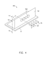
FIG. 4 is a view of the assembled optical communication apparatus of FIG. 1.
FIG. 5 is a cross sectional view of the optical communication apparatus of FIG. 4, taken along line V-V.
FIG. 6 is a cross sectional view of the optical communication apparatus of FIG. 4, taken along line VI-VI.
DETAILED DESCRIPTION
FIGS. 1-3 show an optical communication apparatus 100 according to an exemplary embodiment. The optical communication apparatus 100 includes a substrate 10, two emitters 20, two receivers 30, a detecting unit 40, a lens element 50, two output optical fibers 60 corresponding to the emitters 20, and two input optical fibers 70 corresponding to the receivers 30. The emitters 20, the receivers 30, and the detecting unit 40 are positioned at predetermined positions on the substrate 10.
The substrate 10 supports the emitters 20, the receivers 30, and the detecting unit 40. The substrate 10 includes a printed circuit(s) (not shown) electrically connected to the emitters 20, the receivers 30, and the detecting unit 40.
The emitters 20 generate and emit optical signals. In this embodiment, the emitters 10 are laser diodes. The emitters 20 are a vertical-cavity surface-emitting laser (VCSEL). The receivers 30 receive the optical signals. The receivers 30 are photodiodes. The emitters 20 and the receivers 30 are arranged along a linear direction.
The detecting unit 40 detects an assembling position of the lens element 50 relative to the emitters 20 and the receivers 30. The detecting unit 40 includes a detecting light source 41 and an optical detecting element 42. The detecting light source 41 detects light. The optical detecting element 42 receives the detecting light and determines the assembling position of the lens element 50. The optical detecting element 42 is a charge-coupled device (CCD) or a complementary metal oxide semiconductor (CMOS) device. The detecting unit 40 is positioned in relation to the emitters 20 and the receivers 30 so that it can determine the positions of the emitters 20 and the receivers 30. The detecting light source 41 and the optical detecting element 42 are positioned at opposite ends of the emitters 20 and the receivers 30.
In another embodiment, the detecting light source 41 and/or the optical detecting element 42 can be positioned between any two of the emitters 20 and the receivers 30, or the detecting light source 41 and the optical detecting element 42 can be arranged along a direction different from that of the emitters 20 and the receivers 30.
The lens element 50 includes a first surface 51, a second surface 52, and a first light deflecting surface 53. The first surface 51 is substantially perpendicular to the second surface 52, and the first light deflecting surface 53 forms a 45 degree angle with the first surface 51 and the second surface 52.
The lens element 50 is shaped as a substantially right-angled triangular prism. The first surface 51 and the second surface 52 form the right-angled surfaces of the lens element 50, and the first light deflecting surface 53 forms the bevel surface of the lens element 50. Alternatively, the lens element 50 can be other suitable shapes, such as a quadrangular prism with a cross-section shaped as a substantially right-angled trapezoid.
The lens element 50 includes a number of first communicating lens portions 511 formed on the first surface 51 spatially corresponding to the emitters 20 and the receivers 30. The first lens portions 511 are convex lenses. The lens element 50 further includes a first testing lens portion 512 a spatially corresponding to the detecting light source 41 and a second testing lens portion 512 b spatially corresponding to the optical detecting element 42. The first testing lens portion 512 a and the second testing lens portion 512 b are positioned at opposite ends of the first communicating lens portions 511. The lens element 50 includes a supporting portion 513 protruding from the first surface 51 that surrounds the first communicating lens portions 511, the first testing lens portion 512 a, and the second testing lens portion 512 b. A height of the supporting portion 513 relative to the first surface is greater than the height of the first communicating lens portions 511, the first testing lens portion 512 a, and the second testing lens portion 512 b. The lens element 50 includes a number of second communicating lens portions 521 formed on the second surface 52 corresponding to the first communicating lens portions 511.
The lens element 50 further includes a second light deflecting surface 54 corresponding to the detecting light source 41 and a third light deflecting surface 55 corresponding to the optical detecting element 42. The second light deflecting surface 54 and the third light deflecting surface 55 reflect light at a predetermined angle. The second deflecting surface 54 is substantially perpendicular to the third deflecting surface 55. The second deflecting surface 54 forms a 45 degree angle with an optical axis of the first testing lens portion 512 a, and the third deflecting surface 55 forms a 45 degree angle with an optical axis of the second testing lens portion 512 b. The second deflecting surface 54 and the third deflecting surface 55 are close to each other. The second deflecting surface 54 and the third deflecting surface 55 are located in defined grooves 531 and 532 respectively of the lens element 50. In another embodiment, the grooves 531, 532 can be defined in the second surface 52 or end surfaces of the lens element 50, as long as the second deflecting surface 54 and the third deflecting surface 55 are in predetermined positions.
The output optical fibers 60 and the input optical fibers 70 transmit optical signals. The output optical fibers 60 and the input optical fibers 70 are optically aligned with the second communicating lens portions 521 by a fiber connector (not shown).
Referring to FIGS. 4-6, in assembly, the lens element 50 is supported on the substrate 10 with the first surface 51 facing the substrate 10. The supporting portion 513 contacts the substrate 10 to avoid the first communicating lens portions 511, the first testing lens portion 512 a, and the second testing lens portion 512 b from contacting the substrate 10. The first lens portions 511 are aligned with the emitters 20 and the receivers 30. The first testing lens portion 512 a is aligned with the detecting light source 41. The second testing lens portion 512 b is aligned with the optical detecting element 42. The optical fibers 60 and the input optical fibers 70 are aligned with the second communicating lens portions 521.
During the assembling process of the optical communication apparatus 100, the detecting unit 40 detects an assembling position of the lens element 50 relative to the substrate 10 and determines whether the assembling position is correct. The detecting unit 40 is switched on before the assembling process, and the detecting light source 41 emits detecting light. In assembly, when the first testing lens portion 512 a is positioned in a path of light emitted from the detecting light source 41, the first testing lens portion 512 a converges the light into a parallel light beam. The parallel beam is deflected by the third deflecting surface 54 at a predetermined angle toward the second deflecting surface 55, and the second deflecting surface 55 deflects the parallel beam at a predetermined angle. The parallel light beam deflected by the second deflecting surface 55 passes toward the second testing lens portion 512 b and is converged into a light beam. The converged light beam passes out of the lens element 50 through the second testing lens portion 512 b. When the optical detecting element 42 is in a path of the converged light beam, the optical detecting element 42 receives the converged light beam. Because the position of the detecting unit 40 with relation to the emitters 20 and receivers 30 is predetermined, the correct position for assembly of the lens element 50 is determined according to the position of the converged light beam. Therefore, it is convenient to assemble the lens element 50 onto the substrate 10 with precision, and the assembling efficiency is increased.
In this embodiment, the number of the emitters 20 and the number of the receivers 30 are both two, the number of the first communicating lens portions 511 and the number of the second communicating lens portions 521 are both four, and the number of optical fibers 60 and the number of input optical fibers 70 are both two. The number of emitters 20, receivers 30, first communicating lens portions 511, second communicating lens portions 521, optical fibers 60, and input optical fibers 70 can be changed according to different demands.
It is noted that the detecting unit 40 serves no function in the assembled optical communication apparatus 100. Therefore, the detecting unit 40 can be detached from the substrate 10, allowing the detecting unit 40 to be employed in assembling processes of other similar optical communication apparatuses.
It is believed that the present embodiments and their advantages will be understood from the foregoing description, and it will be apparent that various changes may be made thereto without departing from the spirit and scope of the disclosure or sacrificing all of its material advantages, the examples hereinbefore described merely being preferred or exemplary embodiments of the disclosure.

Claims (13)

What is claimed is:
1. A lens element comprising:
a first surface for facing toward optical emitting elements or optical receiving elements;
a second surface for facing toward optical fibers;
at least one first communicating lens portion on the first surface;
at least one second communicating lens portion on the second surface; and
a first deflecting surface for deflecting optical signals between the least one first communicating lens portion and the at least one second communicating lens portion;
wherein the lens element is shaped as a substantially right-angled triangular prism, the first surface and the second surface are the right-angled surfaces of the lens element, and the first deflecting surface is the bevel surface of the lens element;
wherein the lens element further comprises a first testing lens portion, a second testing lens portion, a second deflecting surface, and a third deflecting surface, the first testing lens portion is configured for converging a detecting light, the second deflecting surface and the third deflecting surface are configured for deflecting the converged detecting light for a predetermined angle to direct the converged detecting light to pass out of the coupling lens through the second testing lens portion;
wherein the second deflecting surface and the third deflecting surface are respectively located in grooves defined in the first deflecting surface.
2. The lens element of claim 1, wherein the first testing lens portion and the second testing lens portion are formed on the first surface.
3. The lens element of claim 2, wherein the at least one first communicating lens portion are arranged along a linear direction on the first surface, and the first testing lens portion and the second testing lens portion are positioned at two opposite sides of the at least one first communicating lens portion.
4. The lens element of claim 1, wherein the lens element comprises a supporting portion protruding from the first surface, and a height of the supporting portion relative to the first surface is larger than a height of each of the at least one first communicating lens portion, the first testing lens portion, and the second testing lens portion.
5. The lens element of claim 1, wherein the second deflecting surface is substantially perpendicular to the third deflecting surface, an angle between the second deflecting surface and an optical axis of the first testing lens portion is about 45 degrees, an angle between the third deflecting surface and an optical axis of the second testing lens portion is about 45 degrees, and the second deflecting surface and the second deflecting surface are gradually close to each other in a direction away from the first surface.
6. The lens element of claim 1, wherein the grooves are separated from each other.
7. An optical communication apparatus, comprising:
a substrate;
an optical emitting or receiving element positioned on the substrate and configured for emitting or receiving optical signals;
an optical fiber corresponding to the optical emitting or receiving element for transmitting the optical signals; and
a lens element comprising:
a first surface facing toward the optical emitting or receiving element;
a second surface facing toward the optical fiber;
a first communicating lens portion on the first surface and spatially corresponding to the optical emitting or receiving element;
a second communicating lens portion on the second surface and spatially corresponding to the optical fibers; and
a first deflecting surface for deflecting the optical signals between the first communicating lens portion and the second communicating lens portion;
wherein the lens element is shaped as a substantially right-angled triangular prism, the first surface and the second surface are the right-angled surfaces of the lens element, and the first deflecting surface is the bevel surface of the lens element;
wherein the lens element further comprises a first testing lens portion, a second testing lens portion, a second deflecting surface, and a third deflecting surface, the first testing lens portion is configured for converging incident detecting light, the second deflecting surface and the third deflecting surface are configured for deflecting the converged detecting light for a predetermined angle to direct the converged detecting light to pass out of the coupling lens through the second testing lens portion;
wherein the second deflecting surface and the third deflecting surface are respectively located in grooves defined in the first deflecting surface.
8. The optical communicating apparatus of claim 7, wherein the optical communicating apparatus comprises a detecting unit for emitting the detecting light to the first testing lens portion, receiving the detecting light passing out of the lens element through the second testing lens portion, and determining an assembling position of the lens element relative to the substrate according to the received detecting light.
9. The optical communicating apparatus of claim 8, wherein the detecting unit comprises a detecting light source spatially corresponding to the first testing lens portion and an optical detecting element spatially corresponding to the second testing lens portion, the detecting light source is configured for emitting the detecting light, and the optical detecting element is configured for receiving the detecting light passing out of the coupling lens through the second testing lens portion and determining the assembling position of the lens element in relation to the substrate according to the received detecting light.
10. The optical communicating apparatus of claim 9, wherein the optical detecting element is selected from one of the group consisting of a charge-coupled device and a complementary metal oxide semiconductor device.
11. The optical communicating apparatus of claim 9, wherein the detecting light source and the optical detecting element are positioned at opposite sides of the optical emitting or receiving element.
12. The optical communicating apparatus of claim 7, wherein the second deflecting surface is substantially perpendicular to the third deflecting surface, an angle between the second deflecting surface and an optical axis of the first testing lens portion is about 45 degrees, an angle between the third deflecting surface and an optical axis of the second testing lens portion is about 45 degrees, and the second deflecting surface and the second deflecting surface are gradually close to each other in a direction away from the first surface.
13. The optical communicating apparatus of claim 7, wherein the grooves are separated from each other.
US13/928,865 2012-12-17 2013-06-27 Lens element and optical communication apparatus with same Expired - Fee Related US9182557B2 (en)

Applications Claiming Priority (2)

Application Number Priority Date Filing Date Title
TW101147758 2012-12-17
TW101147758A TWI575257B (en) 2012-12-17 2012-12-17 Optical coupling lens and optical communication module

Publications (2)

Publication Number Publication Date
US20140169736A1 US20140169736A1 (en) 2014-06-19
US9182557B2 true US9182557B2 (en) 2015-11-10

Family

ID=50930972

Family Applications (1)

Application Number Title Priority Date Filing Date
US13/928,865 Expired - Fee Related US9182557B2 (en) 2012-12-17 2013-06-27 Lens element and optical communication apparatus with same

Country Status (2)

Country Link
US (1) US9182557B2 (en)
TW (1) TWI575257B (en)

Families Citing this family (2)

* Cited by examiner, † Cited by third party
Publication number Priority date Publication date Assignee Title
TW201423035A (en) * 2012-12-14 2014-06-16 Hon Hai Prec Ind Co Ltd Optical coupling lens detection system and method using same
TW201516503A (en) * 2013-10-25 2015-05-01 Hon Hai Prec Ind Co Ltd Optical device

Citations (15)

* Cited by examiner, † Cited by third party
Publication number Priority date Publication date Assignee Title
US3990775A (en) * 1973-07-23 1976-11-09 Bell Telephone Laboratories, Incorporated Thin-film optical waveguide
US4111523A (en) * 1973-07-23 1978-09-05 Bell Telephone Laboratories, Incorporated Thin film optical waveguide
US4445759A (en) * 1980-10-08 1984-05-01 Commissariat A L'energie Atomique Integrated Fresnel lens and its production process
JPS61189504A (en) * 1985-02-19 1986-08-23 Matsushita Electric Ind Co Ltd Preparation of fresnel lens
US4773063A (en) * 1984-11-13 1988-09-20 University Of Delaware Optical wavelength division multiplexing/demultiplexing system
US4930853A (en) * 1988-07-04 1990-06-05 Cselt - Centro Studi E Laboratori Telecomunicazioni S.P.A. Electrooptic deflector
US5122903A (en) * 1989-03-15 1992-06-16 Omron Corporation Optical device and optical pickup device using the same
JPH07221592A (en) * 1994-01-31 1995-08-18 Nec Corp Sound field converging element
US6269203B1 (en) * 1999-03-17 2001-07-31 Radiant Photonics Holographic optical devices for transmission of optical signals
US6271049B1 (en) * 1998-09-14 2001-08-07 Siemens Aktiengesellschaft Method for producing an optoelectronic component
US20040202477A1 (en) * 2003-02-17 2004-10-14 Seiko Epson Corporation Optical module and manufacturing method of the same, optical communication device, opto-electrical hybrid integrated circuit, circuit board, and electronic apparatus
US20070053694A1 (en) * 2005-09-08 2007-03-08 Northrop Grumman Corporation Optical multi-channel free space interconnect
US20080100933A1 (en) * 2006-10-27 2008-05-01 Hon Hai Precision Industry Co., Ltd. Lens module assembly and imaging system having same
US20110267570A1 (en) * 2008-03-03 2011-11-03 Citizen Holdings Co., Ltd. Electro-optical device
US20120155802A1 (en) * 2010-12-16 2012-06-21 Hon Hai Precision Industry Co., Ltd. Optoelectronic transmission device having solar cell unit

Family Cites Families (3)

* Cited by examiner, † Cited by third party
Publication number Priority date Publication date Assignee Title
JPWO2008023508A1 (en) * 2006-08-22 2010-01-07 日本電気株式会社 Optical connector and optical coupling structure
KR101351882B1 (en) * 2006-09-13 2014-01-17 주식회사 와이텔포토닉스 An optical connection component
JP5082894B2 (en) * 2008-01-31 2012-11-28 ソニー株式会社 Photoelectric transmission connector, photoelectric transmission device and electronic equipment

Patent Citations (15)

* Cited by examiner, † Cited by third party
Publication number Priority date Publication date Assignee Title
US3990775A (en) * 1973-07-23 1976-11-09 Bell Telephone Laboratories, Incorporated Thin-film optical waveguide
US4111523A (en) * 1973-07-23 1978-09-05 Bell Telephone Laboratories, Incorporated Thin film optical waveguide
US4445759A (en) * 1980-10-08 1984-05-01 Commissariat A L'energie Atomique Integrated Fresnel lens and its production process
US4773063A (en) * 1984-11-13 1988-09-20 University Of Delaware Optical wavelength division multiplexing/demultiplexing system
JPS61189504A (en) * 1985-02-19 1986-08-23 Matsushita Electric Ind Co Ltd Preparation of fresnel lens
US4930853A (en) * 1988-07-04 1990-06-05 Cselt - Centro Studi E Laboratori Telecomunicazioni S.P.A. Electrooptic deflector
US5122903A (en) * 1989-03-15 1992-06-16 Omron Corporation Optical device and optical pickup device using the same
JPH07221592A (en) * 1994-01-31 1995-08-18 Nec Corp Sound field converging element
US6271049B1 (en) * 1998-09-14 2001-08-07 Siemens Aktiengesellschaft Method for producing an optoelectronic component
US6269203B1 (en) * 1999-03-17 2001-07-31 Radiant Photonics Holographic optical devices for transmission of optical signals
US20040202477A1 (en) * 2003-02-17 2004-10-14 Seiko Epson Corporation Optical module and manufacturing method of the same, optical communication device, opto-electrical hybrid integrated circuit, circuit board, and electronic apparatus
US20070053694A1 (en) * 2005-09-08 2007-03-08 Northrop Grumman Corporation Optical multi-channel free space interconnect
US20080100933A1 (en) * 2006-10-27 2008-05-01 Hon Hai Precision Industry Co., Ltd. Lens module assembly and imaging system having same
US20110267570A1 (en) * 2008-03-03 2011-11-03 Citizen Holdings Co., Ltd. Electro-optical device
US20120155802A1 (en) * 2010-12-16 2012-06-21 Hon Hai Precision Industry Co., Ltd. Optoelectronic transmission device having solar cell unit

Non-Patent Citations (1)

* Cited by examiner, † Cited by third party
Title
K. Takizawa, "Electrooptic Fresnel lens-scanner with an array of channel waveguides," Appl. Opt. 22, 2468-2473 (1983). *

Also Published As

Publication number Publication date
TW201426025A (en) 2014-07-01
TWI575257B (en) 2017-03-21
US20140169736A1 (en) 2014-06-19

Similar Documents

Publication Publication Date Title
US9116312B2 (en) Lens element and optical communication apparatus with same
CN100409054C (en) Small form factor all-polymer optical device with integrated dual beam path based on total internal reflection optical turn
US10976510B2 (en) Optical receptacle and optical module
US9971106B2 (en) Optical receptacle and optical module
US9557499B2 (en) Coupling light from a waveguide array to single mode fiber array
JP2007127797A (en) Optical module
US10048458B2 (en) Optical module
US9912437B2 (en) Optical transmitters
GB2416941A (en) Passive alignment and coupling of an optical fibre with an optoelectonic device using a dual lens arrangement
JP2014115649A (en) Optical communication module with fiber submount and latching optics assembly
US6674941B2 (en) Optical coupling for optical fibers
US9341796B2 (en) Optical coupler and photoelectric conversion device having same
US9182557B2 (en) Lens element and optical communication apparatus with same
US9477054B2 (en) Optical coupling assembly
US9074928B2 (en) Optical connector with enhancing pins securing shell on circuit board
CN103885133A (en) Optical communication device
US9448374B2 (en) Optical communication apparatus having coupler and supporting member connected together
US9658413B2 (en) Optical connector and optical coupling assembly
US9134488B2 (en) Optical coupling connector and optical coupling assembly
US9477053B2 (en) Optical coupling lens and optical coupling module
US9268105B2 (en) Optical connector
WO2020153238A1 (en) Optical connector, optical cable, and electronic apparatus
US10656349B2 (en) Optical coupler and optical fiber passive alignment
US20120134626A1 (en) Optoelectronic module and light transmitting and receiving module having same
US20200166719A1 (en) Optical receptacle and optical module

Legal Events

Date Code Title Description
AS Assignment

Owner name: HON HAI PRECISION INDUSTRY CO., LTD., TAIWAN

Free format text: ASSIGNMENT OF ASSIGNORS INTEREST;ASSIGNOR:HUNG, YI;REEL/FRAME:030701/0388

Effective date: 20130624

STCF Information on status: patent grant

Free format text: PATENTED CASE

FEPP Fee payment procedure

Free format text: MAINTENANCE FEE REMINDER MAILED (ORIGINAL EVENT CODE: REM.); ENTITY STATUS OF PATENT OWNER: LARGE ENTITY

LAPS Lapse for failure to pay maintenance fees

Free format text: PATENT EXPIRED FOR FAILURE TO PAY MAINTENANCE FEES (ORIGINAL EVENT CODE: EXP.); ENTITY STATUS OF PATENT OWNER: LARGE ENTITY

STCH Information on status: patent discontinuation

Free format text: PATENT EXPIRED DUE TO NONPAYMENT OF MAINTENANCE FEES UNDER 37 CFR 1.362

FP Expired due to failure to pay maintenance fee

Effective date: 20191110