US8854527B2 - Optical lens having fixed lenses and embedded active optics - Google Patents
Optical lens having fixed lenses and embedded active optics Download PDFInfo
- Publication number
- US8854527B2 US8854527B2 US13/318,440 US201013318440A US8854527B2 US 8854527 B2 US8854527 B2 US 8854527B2 US 201013318440 A US201013318440 A US 201013318440A US 8854527 B2 US8854527 B2 US 8854527B2
- Authority
- US
- United States
- Prior art keywords
- lens
- optical
- enclosure
- optical lens
- optical element
- Prior art date
- Legal status (The legal status is an assumption and is not a legal conclusion. Google has not performed a legal analysis and makes no representation as to the accuracy of the status listed.)
- Expired - Fee Related, expires
Links
Images


Classifications
-
- H04N5/2254—
-
- H—ELECTRICITY
- H04—ELECTRIC COMMUNICATION TECHNIQUE
- H04N—PICTORIAL COMMUNICATION, e.g. TELEVISION
- H04N23/00—Cameras or camera modules comprising electronic image sensors; Control thereof
- H04N23/50—Constructional details
-
- H—ELECTRICITY
- H04—ELECTRIC COMMUNICATION TECHNIQUE
- H04N—PICTORIAL COMMUNICATION, e.g. TELEVISION
- H04N23/00—Cameras or camera modules comprising electronic image sensors; Control thereof
- H04N23/57—Mechanical or electrical details of cameras or camera modules specially adapted for being embedded in other devices
-
- H04N5/2257—
-
- Y—GENERAL TAGGING OF NEW TECHNOLOGICAL DEVELOPMENTS; GENERAL TAGGING OF CROSS-SECTIONAL TECHNOLOGIES SPANNING OVER SEVERAL SECTIONS OF THE IPC; TECHNICAL SUBJECTS COVERED BY FORMER USPC CROSS-REFERENCE ART COLLECTIONS [XRACs] AND DIGESTS
- Y10—TECHNICAL SUBJECTS COVERED BY FORMER USPC
- Y10T—TECHNICAL SUBJECTS COVERED BY FORMER US CLASSIFICATION
- Y10T29/00—Metal working
- Y10T29/49—Method of mechanical manufacture
- Y10T29/49002—Electrical device making
- Y10T29/49004—Electrical device making including measuring or testing of device or component part
Definitions
- This invention relates generally to optical devices and assemblies and, more specifically, to lenses having active optical control.
- Lens structures for optical devices such as cameras consist of multiple lens elements assembled in a single barrel or stacked in a wafer form, utilizing spacers, to create fixed focus lens assemblies. These lens structures have a fixed focal plane and are mechanically moved to focus on objects in varying distances to the camera system.
- Tunable liquid crystal lenses that have a flat layer construction are known in the art, as described in PCT patent application WO 2007/098602, published on Sep. 7, 2007, as well as in PCT patent application WO 2009/153764 published Dec. 23, 2009, the specifications of which are hereby incorporated by reference as if fully set forth herein.
- an electrically controllable optical lens apparatus that has a first optical lens and a second optical lens fixed in position relative to each other such that an optical signal can pass through both lenses.
- an electrically controllable active optical element Located at a fixed position within the apparatus, which in a first embodiment is a position between the first and second lenses, is an electrically controllable active optical element.
- the active optical element which may be, for example, a tunable liquid crystal lens (TLCL), changes its optical characteristics from a first state to a second state in response to an input electrical signal, such that it exerts a different optical influence on the optical signal in the first state than in the second state.
- the active optical element may change between many states, changing the overall optical power of the entire lens apparatus.
- the lens apparatus has the active optical element positioned within a lens stack.
- the active optical element by applying a required electrical signal to the active element, the optical properties of the lens assembly are modified without any mechanical movement.
- the focal plane of the lens structure could be moved, thus creating a variable focus (e.g. auto focus) device.
- the active element can function as an aperture stop, shutter, IR cut filter or other mechanism in the lens stack, resulting in a possibly shorter and improved overall lens design.
- the aperture of the TLCL can be smaller than if the TLCL is located outside the stack (typically 25% smaller).
- a lens mounting structure having a barrel shape is used to enable easy assembly of the active element into the lens stack.
- a lens barrel is split into two sections at the active optical element plane.
- Mechanical features on the fixed focus lens elements are used to establish assembly spacing and alignment.
- the active optical element is designed to be integrated into the stack without interfering with precise alignment and spacing of other optical elements within the stack.
- a special feature on the fixed elements is used to align and space these elements without interference from the active optical element.
- the active optical element may have a substantially planar shape and, in one embodiment, is roughly square. With such a square shape, extra space around the active optical element may be used to provide alignment and spacing, which is required in conventional fixed lens systems to achieve acceptable optical performance.
- An integrated electrical connection structure and method is also provided to enable electrical contacts as part of the lens barrel assembly.
- At least one electrical contact provides an electrically conductive path between an outer surface of the lens mounting structure and the active optical element.
- the contact may be a stamped metallic piece with an incorporated spring element to ensure reliable electrical connection to a contact on a receiving device to which the lens apparatus is mounted.
- a molded interconnect device also may be used to create a connection between the active optical element and camera housing or surrounding devices. An MID would be used in place of lead frames in the device. Connection to the embedded active optical element may be achieved by means of conductive adhesives.
- the first is a threaded barrel with appropriate matching threads on the housing of a receiving device to which the lens apparatus is mounted.
- a ramp design is used to ensure proper positioning of the contacts with respect to corresponding contacts on the camera housing.
- a single thread is created with a locking stop mechanism to define the distance of lens barrel from the sensor in a deterministic way.
- no focusing operation is required at assembly and optical device relies solely on the active optical element for proper focusing.
- FIG. 1 is a cross sectional view of a first embodiment of a lens structure according to the present invention
- FIG. 2 is a perspective view of the lens structure of FIG. 1 .
- FIG. 2A is an isolated view of an outer portion of the lens structure of FIG. 1 showing an active optical element adjacent thereto.
- FIG. 3 is a perspective view of a lens structure according to the present invention that uses a ramp structure and electrical connections near a top of a barrel portion of the lens structure.
- FIG. 4 is a perspective view of a lens structure according to the present invention that uses electrical connections on an inner surface of an inner portion of the lens structure.
- FIG. 5 is a cross sectional view of a lens structure according to the present invention in which fixed lenses are formed on the surfaces the upper and lower substrates of an active optical element.
- FIG. 6 is a perspective view of a lens structure according to the present invention in which a molded interconnect device is used to provide electrical connection between an active optical element and an inner surface of an outer portion of the lens structure.
- FIG. 6A is a perspective view of an interior of an outer portion of the structure of FIG. 6 showing the location of electrical contact points.
- FIG. 6B is a top view of an interior of the lens structure of FIG. 6 showing an active optical element in place adjacent to the electrical contact points of the lens structure.
- FIG. 7 is a perspective view of a lens structure according to the present invention in which a molded interconnect device is used to provide electrical connection between an active optical element and an inner surface of an inner portion of the lens structure.
- FIG. 7A is a perspective view of an interior of an inner portion of the lens structure of FIG. 7 showing the location of electrical contact points.
- FIG. 8 is a perspective view of a lens structure according to the present invention showing gaps via which an electrically conductive adhesive may be applied to the connection points between an active optical element and the electrical contacts of the lens structure.
- FIG. 9 is a perspective view of a single barrel configuration in which the present invention may be used, the figure depicting a socket flange base in an exploded view showing the image sensor, circuit board and the various optical elements.
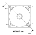
- FIG. 10A is a top view of an assembly including a unitary image sensor and barrel lens mounting that has a tunable liquid crystal device to provide a tunable focus camera.
- FIG. 10B is a cross sectional side view of the assembly of FIG. 10A .
- FIG. 11A is a top view of an assembly including a unitary image sensor, a barrel lens mounting and a tunable liquid crystal device, and that functions as a fixed focus camera.
- FIG. 11B is a cross sectional side view of the assembly of FIG. 11A .
- FIG. 12A is a top view of an assembly similar to that of FIGS. 11A and 11B , but that has the tunable liquid crystal device located between two lens elements of the structure.
- FIG. 12B is a cross sectional side view of FIG. 12A .
- FIG. 13A is a cross sectional view of a unitary image sensor and barrel lens mounting that has a top cavity for receiving the tunable liquid crystal lens device after assembly of the image sensor and barrel lens.
- FIG. 13B is a perspective view of the assembly of FIG. 13A with a top cover of the assembly removed.
- the present invention is directed to an optical lens apparatus that uses fixed lenses in combination with an electrically controllable liquid crystal optical device.
- the apparatus may be directed to one of several applications.
- the apparatus has an overall “barrel structure” and uses the optical properties of the fixed lenses in combination with the electrically controlled optical properties of the liquid crystal device.
- FIG. 1 Shown in FIG. 1 is a schematic view of a first embodiment of the invention in which a variable focus lens 10 has a barrel structure consisting of two portions, an outer portion 12 and an inner portion 14 .
- the lens may be used in a variety of different applications, including compact digital cameras, such as might be integrated into a portable telephone.
- Each of the two portions includes a fixed lens, lens 16 in the outer portion 12 , and lens 18 in the inner portion 14 .
- Light from a subject in front of the outer portion 12 is collected via aperture 20 and focused by the outer portion fixed lens 16 .
- This focused light is refocused by the fixed lens 18 of the inner portion to form an image on a desired imaging device, such as a CMOS or a charge-coupled device type detector, etc. (not shown).
- the overall focusing of the variable focus lens 10 is, however, adjustable by way of a tunable lens 22 positioned between the fixed lens 16 and the fixed lens 18 .
- the tunable lens 22 is a tunable liquid crystal lens (TLCL), such as that discussed in PCT patent application publication WO 2009/153764 published Dec. 23, 2009, the substance of which is incorporated herein by reference.
- a TLCL is a liquid crystal based lens structure for which the focusing power changes with changes to an applied electric field.
- the tuning range of the TLCL may include a zero optical power level at which it adds no focusing effect to the overall lens structure.
- the electrical signal supplied to the TLCL changes, the optical power of the lens changes with it, causing an overall change in the focal length of the variable focus lens 10 .
- variable focus lens 10 The two portions of the variable focus lens 10 are shown separated from each other in FIG. 1 , but are part of a single integral component during operation. In the present embodiment, the two portions are separate and are joined together at the position of the active optical plane, i.e., the location of the TLCL.
- the variable focus lens When assembled, the variable focus lens has a “barrel” shape, as is evident in the perspective view of FIG. 2 .
- the barrel shape has a thread 24 along its curved outer surface, allowing the variable lens to be screwed into a threaded hole on an apparatus (such as a camera) on which it is installed, although other connection means may be used instead.
- FIG. 2 Also shown in FIG. 2 are a set of electrical contacts 26 by which electrical connection with the TLCL may be made. These contacts can be stamped metallic pieces with incorporated spring elements that help ensure reliable electrical connection. Corresponding electrical contacts on the apparatus to which the lens is mounted allow convenient electrical signal routing.
- the relative positioning of the TLCL 22 which in this embodiment has a generally square shape, and the outer portion 12 of the barrel structure is shown in the isolated view of FIG. 2A .
- This figure provides a view of the interior of the barrel structure, and shows how electrical contacts located in the corners of the TLCL 22 make contact with the electrical contacts 26 of the barrel structure.
- electrical continuity is easily provided from a surface of the apparatus to which the lens is mounted to the electrically-activated TLCL 22 on the interior of the lens structure.
- FIG. 3 An alternative arrangement for assembly of the system uses a ramp or cam surface 28 on the barrel of the lens 10 , as is shown in FIG. 3 .
- This ramp allows for barrel adjustment during assembly.
- the ramp is essentially a circumferential lip that extends radially from an outer surface of the barrel, and that includes a flat surface 29 that functions as a stop mechanism during rotation of the barrel.
- the ramp 28 makes contact with a corresponding ramp on an inner surface of the mounting socket (not shown).
- the two ramps slide against each other until the flat surface 29 of the ramp 28 meets a corresponding flat surface of the mounting socket.
- the barrel when the barrel is attached to the housing of the corresponding optical device using the ramp method, the barrel stops in a predetermined position with respect to an internal component of the device, such as a CMOS sensor.
- the barrel may then be permanently attached to the device using, for example, adhesive or ultrasonic welding, or any other technique known in the art. Using this arrangement, no focusing operation is required at assembly, and the optical variable lens 10 relies solely on the TLCL for proper focusing.
- CMOS complementary metal-sonic welding
- FIG. 4 Another embodiment of the present invention is shown in FIG. 4 , and makes use of electrical contacts located at the innermost surface of the barrel structure. This is in contrast to the positioning of the contacts on an inner surface of the outer portion 12 , as shown, for example, in FIG. 2 .
- the electrical contacts 26 pass between the outer portion 12 and the inner portion 14 to make contact with the TLCL.
- the contacts of the FIG. 4 embodiment extend to a surface of the inner portion 14 , where they will make contact with corresponding contacts of the apparatus to which the variable lens is mounted 10
- those of the FIG. 2 embodiment are extended to the aforementioned inner surface of the outer portion.
- the particular configuration of the contacts in one of these two arrangements is a matter of design convenience.
- a fixed lens integral with the TLCL is used.
- the TLCL includes a fixed lens 30 molded onto its surface. Further disclosure of such a lens construction set out in PCT patent application publication WO/2010/022503 published Mar. 4, 2010, the specification of which is hereby incorporated by reference.
- FIG. 6 shows another variation of the present invention in which a molded interconnect device (MID) approach is used to create a connection between the active optical element and the camera housing or surrounding devices.
- MID molded interconnect device
- This embodiment is similar to that shown in FIG. 2 , but in place of stamped metal contact pieces, MID elements 32 are used.
- the MID elements pass in between the inner portion 14 and the outer portion 12 of the barrel and make electrical connection to the embedded active optical element by way of conductive adhesives.
- the MID elements may form contact surfaces 34 on an interior of the outer portion 12 of the barrel, as is shown in FIG. 6A . These contact surfaces 34 allow for an easy means of making an electrical connection to the active optical element such as a TLCL 22 .
- FIG. 6 shows another variation of the present invention in which a molded interconnect device (MID) approach is used to create a connection between the active optical element and the camera housing or surrounding devices.
- MID elements 32 are used.
- the MID elements pass in between the inner portion 14 and the outer
- 6B is a view of the outer portion 12 with a TLCL 22 having the corners of its square shape positioned adjacent to the contact surfaces 34 .
- Surface electrical contacts located in the corners of the TLCL 22 thereby make electrical contact with the contact surfaces 34 of the outer portion.
- the MID contacts may also extend to an inner surface of the inner portion 14 .
- the MID contacts 36 are positioned to make contact with corresponding contacts on a surface of the device to which the lens structure is attached.
- the MID contacts 36 in this embodiment extend along an interior surface of the inner portion 14 to locations adjacent to the active optical element. This is shown more clearly in FIG. 7A , which is an isolated view of the inner portion 12 of FIG. 7 as seen from the opposite side.
- active optical element such as a TLCL 22
- TLCL 22 the active optical element
- those skilled in the art will understand that such an element with a square shape could rest within the barrel with corresponding electrical contacts located in the corners of the square shape located adjacent to the interior surfaces of the MID contacts 36 .
- the two portions may be constructed such that, when assembled together, small gaps remain between them in the vicinity of the electrical contacts.
- gaps 38 are shown in the perspective view of FIG. 8 , although it will be understood by those skilled in the art that such gaps may be used with any of the embodiments described herein. Since the electrical contacts of the active optical element will reside adjacent to the electrical contacts of the barrel assembly, gaps 38 may serve as access points by which to apply a conductive adhesive that both secures the electrical components together and provides a more robust electrical connection between them.
- the barrel can be provided with a base, for example incorporating a flange, and that electrical connections between the active embedded optical element and the circuit board may be through the barrel base.
- the barrel body incorporates the required conductors to conduct signals from the circuit board to the contacts on the barrel body in contact with the active element.
- FIG. 9 illustrates a conventional single barrel having a socket flange base in an exploded view showing the image sensor 40 , circuit board 42 and the various optical elements, including fixed lenses 44 , IR glass 46 and TLCL 47 , which is protected by barrel cover 48 .
- the base contacts and integration of the conductors and embedded active optical element contacts are not detailed in FIG. 9 .
- An arrangement such as shown in this figure may be used with the present invention. In such a case, the barrel body shown in FIG. 9 would be one of those presented in the foregoing embodiments, with the active optical element positioned therewithin between the two barrel portions.
- the present invention also includes the possibility of using active optical devices other than lenses in a configuration such as that presented herein.
- active optical devices other than lenses in a configuration such as that presented herein.
- an electrically activated shutter may be provided in an arrangement similar to that shown in FIG. 1 .
- FIGS. 10A and 10B there is shown a design for incorporation of a barrel with an active optical element (in this case a TLCL) into a camera module unit.
- FIG. 10A is a top view of the device, and indicates the section line corresponding to the cross-sectional view of FIG. 10B .
- the barrel i.e., lens/TLCL assembly
- housing assembly 52 which is mounted to PC board substrate 54 , which also supports image sensor 56 . It is beneficial in this, and other, embodiments that the two fixed lens components make contact with each other to ensure a proper alignment and orientation between them.
- the housing is threaded to receive the threaded barrel assembly, and includes four metallic inserts 58 , such as lead frames, for completing connection from the barrel assembly 50 to the camera substrate. Since the barrel assembly 50 includes conductive contacts 51 that are electrically connected to the active optical element 53 , the metallic inserts 58 provide the necessary electrical pathways to the substrate. Thus, this configuration allows electrical connection between the active optical element 53 and the substrate 54 , despite the fact that the barrel assembly may have imprecise height and rotational angle relative to the housing.
- the metallic inserts 58 are electrically connected to the board 54 using conductive glue 60 , although solder could also be used.
- the housing 52 itself is also connected to the substrate 54 using glue (typically non-conductive), but bumps 62 are provided on the bottom of the housing surface which extend beyond the glue to make contact with the substrate 54 . In this way, a precise distance is maintained between the housing 52 and the substrate 54 which is not affected by the thickness or flatness of the glue layer.
- FIGS. 11A and 11B there is shown a fixed focus camera module.
- FIG. 11A is a top view of the device, and shows a section line along which the cross section of FIG. 11B is taken.
- Two lens elements 64 are permanently mounted within a housing 66 with no adjustability for focus.
- a TLCL 68 is located at the side of the housing opposite PC board substrate 70 , to which is mounted image sensor 72 .
- electrical connection is made between the substrate and the TLCL via metallic inserts 74 that run vertically in the corners of the housing, being connected to the substrate via conductive glue 76 .
- metallic inserts 74 that run vertically in the corners of the housing, being connected to the substrate via conductive glue 76 .
- the housing 66 also makes use of bumps at its base to provide a precise setoff between the housing and the substrate 70 .
- a top cover 78 of the housing blocks light except that in the main optical path, and provides mechanical protection to TLCL 68 , which is mounted at the top of the device, above the fixed lenses.
- a focus-free camera module refers to a camera module that is constructed by utilizing a camera housing with lenses integrated into the housing permanently before attachment to the sensor substrate.
- a configuration such as that shown in FIGS. 11A and 11B .
- the main issue with such a construction is that the tolerances of the assembly (physical and optical) may not be tight enough to ensure a precise focus at the sensor surface, and an out-of-focus image may result.
- minute focus errors may be compensated for by adjusting the optical power of the TLCL 68 .
- a focus-free camera module uses an active optical element (TLCL 80 ) is located between primary lens 82 and secondary lens 84 of the lens stack.
- TLCL 80 active optical element
- This configuration is similar to that of FIG. 11 , except for the location of the TLCL.
- a focus plane of the lens structure can be actively adjusted by changing the optical power of the TLCL 80 to compensate for an improper distance of the lens stack from the sensor 85 .
- this design enables construction of cheaper cameras, utilizing parts with usual tolerances and without any focusing operation.
- FIG. 12A shows the location of metallic inserts 86 along the side edges of the lens housing 88 .
- the metallic inserts do not run all the way to the top of the housing but, rather, only to the vertical position of the TLCL 80 .
- the inserts 86 are connected to the substrate 87 using conductive glue 90 , and the housing has a setoff bump, as in the previous embodiments. This configuration, along with the capability of the embedded TLCL to adjust the focus plane, can enable proper camera focus without adjustment of the barrel.
- the camera need not be a fixed-focus camera.
- This design shows an easy and low cost way of incorporating a TLCL 94 into a conventional camera module.
- a camera housing 96 is designed and molded in such a way that there is a cavity on the top of the housing to receive the TLCL, while allowing for a barrel-type lens to be inserted into a socket in the housing before inserting the TLCL.
- the TLCL 94 resides directly adjacent to the lens barrel 98 , in close proximity to the lens elements.
- Connection is provided by metallic inserts 100 , as apparent from FIG. 13B , which shows the housing with top cover 95 removed.
- connectors can also be seen in the cross sectional view of FIG. 13A which, like earlier embodiments, is taken along a diagonal section line.
- This embodiment may also use a conductive glue to connect the metallic inserts to the substrate 102 and the setoff bumps that function as in the previous embodiments.
- This camera module can include a conventional lens barrel 98 that is threaded into the housing.
- One possible assembly sequence for the assembly of this embodiment is to attach the housing, including the lens barrel, to the substrate 102 that supports the CMOS sensor.
- the electrical contacts 100 in the housing can be connected to the substrate by the conductive adhesive over the connection pads on the camera substrate.
- the lens barrel 98 is turned and focused, as is done in conventional camera modules, and glue added to the threads to fix the barrel in the desired position.
- the bare TLCL 94 (TLCL part with no housing or FPC) is placed into the top cavity and aligned with respect to the lens barrel aperture.
- conductive adhesive is applied to connect the contacts on the TLCL to the electrical contacts in the housing, after which the top cover 95 is placed over the TLCL 94 to close the housing. In an arrangement such as this, therefore, focus tuning of the device can be done manually and by adjustment of the TLCL.
- the active optical element can be placed on the top, in the middle, or on the bottom of other lens elements depending on the optical design of the fixed element lenses. In each of these cases electrical connections can be made similarly. It will also be appreciated that, in terms of construction, the lens barrel can be constructed in two pieces or as a single piece.
Abstract
Description
Claims (30)
Priority Applications (1)
| Application Number | Priority Date | Filing Date | Title |
|---|---|---|---|
| US13/318,440 US8854527B2 (en) | 2009-05-03 | 2010-05-03 | Optical lens having fixed lenses and embedded active optics |
Applications Claiming Priority (4)
| Application Number | Priority Date | Filing Date | Title |
|---|---|---|---|
| US17502509P | 2009-05-03 | 2009-05-03 | |
| US61175025 | 2009-05-03 | ||
| US13/318,440 US8854527B2 (en) | 2009-05-03 | 2010-05-03 | Optical lens having fixed lenses and embedded active optics |
| PCT/US2010/033347 WO2010129454A1 (en) | 2009-05-03 | 2010-05-03 | Optical lens having fixed lenses and embedded active optics |
Publications (2)
| Publication Number | Publication Date |
|---|---|
| US20120092543A1 US20120092543A1 (en) | 2012-04-19 |
| US8854527B2 true US8854527B2 (en) | 2014-10-07 |
Family
ID=42735392
Family Applications (2)
| Application Number | Title | Priority Date | Filing Date |
|---|---|---|---|
| US13/318,559 Abandoned US20120200764A1 (en) | 2009-05-03 | 2010-05-03 | Camera module with tolerance adjustment using embedded active optics |
| US13/318,440 Expired - Fee Related US8854527B2 (en) | 2009-05-03 | 2010-05-03 | Optical lens having fixed lenses and embedded active optics |
Family Applications Before (1)
| Application Number | Title | Priority Date | Filing Date |
|---|---|---|---|
| US13/318,559 Abandoned US20120200764A1 (en) | 2009-05-03 | 2010-05-03 | Camera module with tolerance adjustment using embedded active optics |
Country Status (2)
| Country | Link |
|---|---|
| US (2) | US20120200764A1 (en) |
| WO (2) | WO2010129454A1 (en) |
Cited By (1)
| Publication number | Priority date | Publication date | Assignee | Title |
|---|---|---|---|---|
| US10732376B2 (en) * | 2015-12-02 | 2020-08-04 | Ningbo Sunny Opotech Co., Ltd. | Camera lens module and manufacturing method thereof |
Families Citing this family (50)
| Publication number | Priority date | Publication date | Assignee | Title |
|---|---|---|---|---|
| WO2010129454A1 (en) | 2009-05-03 | 2010-11-11 | Lensvector, Inc. | Optical lens having fixed lenses and embedded active optics |
| WO2011008443A2 (en) | 2009-06-29 | 2011-01-20 | Lensvector Inc. | Wafer level camera module with active optical element |
| KR20110064156A (en) * | 2009-12-07 | 2011-06-15 | 삼성전자주식회사 | Imaging device and its manufacturing method |
| CN102238319A (en) * | 2010-04-26 | 2011-11-09 | 鸿富锦精密工业(深圳)有限公司 | Image pickup device |
| TWI484243B (en) * | 2010-06-10 | 2015-05-11 | Hon Hai Prec Ind Co Ltd | Lens module and camera device |
| WO2012037343A1 (en) * | 2010-09-15 | 2012-03-22 | Ascentia Imaging, Inc. | Imaging, fabrication, and measurement systems and methods |
| US10132925B2 (en) | 2010-09-15 | 2018-11-20 | Ascentia Imaging, Inc. | Imaging, fabrication and measurement systems and methods |
| US9065991B2 (en) | 2010-11-04 | 2015-06-23 | Lensvector Inc. | Methods of adjustment free manufacture of focus free camera modules |
| TWI490584B (en) * | 2010-11-15 | 2015-07-01 | Hon Hai Prec Ind Co Ltd | Lens module, camera module and method for making lens module |
| CN102466844B (en) * | 2010-11-16 | 2016-08-10 | 鸿富锦精密工业(深圳)有限公司 | The manufacture method of lens assembly, image-taking device and lens assembly |
| JP5617561B2 (en) * | 2010-11-25 | 2014-11-05 | 株式会社リコー | Imaging device |
| US8559806B2 (en) * | 2010-12-29 | 2013-10-15 | Samsung Electro-Mechanics Co., Ltd. | Camera module and method for manufacturing the same |
| WO2012116302A2 (en) * | 2011-02-24 | 2012-08-30 | Flextronics Ap, Llc | Autofocus-zoom camera module integrating liquid crystal device as high speed shutter |
| US9172856B2 (en) * | 2011-03-29 | 2015-10-27 | Microsoft Technology Licensing, Llc | Folded imaging path camera |
| KR101944280B1 (en) | 2011-05-18 | 2019-01-31 | 엘지이노텍 주식회사 | Camera Module |
| KR101879662B1 (en) * | 2011-09-16 | 2018-07-19 | 엘지이노텍 주식회사 | Camera module |
| TW201316074A (en) * | 2011-10-05 | 2013-04-16 | Largan Precision Co Ltd | Camera module |
| US9739864B2 (en) | 2012-01-03 | 2017-08-22 | Ascentia Imaging, Inc. | Optical guidance systems and methods using mutually distinct signal-modifying |
| EP2801077B1 (en) | 2012-01-03 | 2023-11-29 | Ascentia Imaging, Inc. | Coded localization systems, methods and apparatus |
| WO2013136053A1 (en) * | 2012-03-10 | 2013-09-19 | Digitaloptics Corporation | Miniature camera module with mems-actuated autofocus |
| US9294667B2 (en) | 2012-03-10 | 2016-03-22 | Digitaloptics Corporation | MEMS auto focus miniature camera module with fixed and movable lens groups |
| WO2013142288A1 (en) * | 2012-03-21 | 2013-09-26 | Optovue, Inc. | Fundus camera |
| KR101940478B1 (en) * | 2012-05-07 | 2019-01-21 | 엘지이노텍 주식회사 | Camera Module |
| KR101917221B1 (en) * | 2012-06-29 | 2018-11-13 | 엘지이노텍 주식회사 | Camera module |
| KR102080790B1 (en) * | 2012-07-09 | 2020-02-24 | 엘지이노텍 주식회사 | Camera Module |
| KR102059169B1 (en) * | 2012-07-30 | 2019-12-24 | 엘지이노텍 주식회사 | Camera Module |
| KR102047373B1 (en) * | 2012-07-30 | 2019-11-21 | 엘지이노텍 주식회사 | Camera Module |
| KR102107654B1 (en) * | 2012-07-30 | 2020-05-07 | 엘지이노텍 주식회사 | Camera Module |
| US9715612B2 (en) | 2012-12-26 | 2017-07-25 | Cognex Corporation | Constant magnification lens for vision system camera |
| US10712529B2 (en) | 2013-03-13 | 2020-07-14 | Cognex Corporation | Lens assembly with integrated feedback loop for focus adjustment |
| US11002854B2 (en) | 2013-03-13 | 2021-05-11 | Cognex Corporation | Lens assembly with integrated feedback loop and time-of-flight sensor |
| US9671671B2 (en) * | 2013-10-10 | 2017-06-06 | Stmicroelectronics Pte Ltd | Optical assembly including electrically conductive coupling member and related methods |
| CN110082883B (en) | 2013-10-11 | 2022-07-29 | 特励达弗莱尔有限责任公司 | Optical barrel assembly, camera including optical barrel assembly, analyte detector including optical barrel assembly, and related methods |
| KR102122550B1 (en) * | 2013-11-05 | 2020-06-26 | 엘지이노텍 주식회사 | Camera module |
| US20150138420A1 (en) * | 2013-11-21 | 2015-05-21 | Stmicroelectronics Pte Ltd. | Liquid crystal cell connection to lens mount of camera module |
| US9369170B2 (en) * | 2014-03-04 | 2016-06-14 | Michael Sorrentino | Mobile device case with movable camera cover |
| US10830927B2 (en) * | 2014-05-06 | 2020-11-10 | Cognex Corporation | System and method for reduction of drift in a vision system variable lens |
| US10795060B2 (en) * | 2014-05-06 | 2020-10-06 | Cognex Corporation | System and method for reduction of drift in a vision system variable lens |
| US9703173B2 (en) | 2015-04-21 | 2017-07-11 | Apple Inc. | Camera module structure having electronic device connections formed therein |
| US10126114B2 (en) | 2015-05-21 | 2018-11-13 | Ascentia Imaging, Inc. | Angular localization system, associated repositionable mechanical structure, and associated method |
| US10261001B2 (en) * | 2015-10-21 | 2019-04-16 | Flir Detection, Inc. | Manually operated desorber for sensor detector device |
| EP3770650B1 (en) | 2016-04-29 | 2022-11-16 | LG Innotek Co., Ltd. | Camera module including liquid lens |
| US11150438B2 (en) | 2016-08-10 | 2021-10-19 | Apple Inc. | Protected interconnect for solid state camera module |
| KR102116999B1 (en) * | 2019-12-18 | 2020-06-02 | 엘지이노텍 주식회사 | Camera Module |
| KR102202197B1 (en) * | 2020-02-18 | 2021-01-13 | 엘지이노텍 주식회사 | Camera Module |
| CN111447350B (en) * | 2020-05-15 | 2022-02-08 | Oppo广东移动通信有限公司 | Camera module and electronic equipment |
| CN114070966B (en) * | 2020-08-04 | 2023-07-07 | 宁波舜宇光电信息有限公司 | Camera module and terminal equipment |
| CN112548833A (en) * | 2020-12-29 | 2021-03-26 | 南京波特光电有限公司 | Optical lens polishing control system |
| US20220294942A1 (en) * | 2020-12-31 | 2022-09-15 | Flir Commercial Systems, Inc. | Light weight lens barrel systems and methods |
| CN112904523B (en) * | 2021-01-15 | 2022-12-13 | 业成科技(成都)有限公司 | Lens structure, display device and wearable equipment |
Citations (35)
| Publication number | Priority date | Publication date | Assignee | Title |
|---|---|---|---|---|
| US4781445A (en) | 1984-02-23 | 1988-11-01 | Canon Kabushiki Kaisha | Optical device having positionally changeable optical surfaces and a method of varying an image forming position |
| US5808679A (en) | 1996-09-06 | 1998-09-15 | Microtek International Inc. | Camera lens assembly using rotatable conductive plate connectors |
| US6359674B1 (en) | 1999-06-08 | 2002-03-19 | Olympus Optical Co., Ltd. | Liquid crystal lens, liquid crystal lens unit, and liquid crystal lens assembly |
| US20040184163A1 (en) | 2003-02-13 | 2004-09-23 | Olympus Corporation | Optical apparatus |
| JP2005084387A (en) | 2003-09-09 | 2005-03-31 | Konica Minolta Opto Inc | Imaging lens and imaging apparatus |
| US20060103758A1 (en) | 2004-11-12 | 2006-05-18 | Samsung Techwin Co., Ltd. | Camera module and method of manufacturing the same |
| US20060203875A1 (en) | 2003-09-26 | 2006-09-14 | Henryk Frenzel | Optical module comprising an image sensor and a lens unit that is supported on the sensitive surface of the image sensor |
| JP2006243573A (en) | 2005-03-07 | 2006-09-14 | Citizen Watch Co Ltd | Liquid crystal lens and camera module |
| US20070031137A1 (en) | 2003-09-26 | 2007-02-08 | Siemens Ag | Optical module comprising a spacer element between the housing of a semiconductor element and a lens unit |
| US20070063048A1 (en) | 2005-09-14 | 2007-03-22 | Havens William H | Data reader apparatus having an adaptive lens |
| WO2007098602A1 (en) | 2006-03-03 | 2007-09-07 | UNIVERSITé LAVAL | Method and apparatus for spatially modulated electric field generation and electro-optical tuning using liquid crystals |
| US20070242173A1 (en) | 2004-11-02 | 2007-10-18 | Blum Ronald D | Electro-active spectacles and method of fabricating same |
| WO2008041469A1 (en) | 2006-10-03 | 2008-04-10 | Panasonic Corporation | Imaging device |
| US20080088756A1 (en) | 2006-09-05 | 2008-04-17 | Ling-Yuan Tseng | Tunable liquid crystal lens module |
| JP2008092314A (en) * | 2006-10-03 | 2008-04-17 | Matsushita Electric Ind Co Ltd | Photographing apparatus |
| US7369327B1 (en) | 1998-06-09 | 2008-05-06 | Olympus Corporation | Variable optical-property element and optical apparatus including the same |
| US20080144186A1 (en) | 2006-12-15 | 2008-06-19 | Chen Feng | Focus module and components with actuator polymer control |
| US20080165427A1 (en) | 2007-01-09 | 2008-07-10 | Cheng-Te Tseng | Image capturing device |
| KR100856092B1 (en) | 2007-06-18 | 2008-09-02 | 삼성전기주식회사 | Optical lens and camera module combined it |
| US20080251707A1 (en) | 2001-10-23 | 2008-10-16 | Tessera North America | Optical chassis, camera having an optical chassis, and associated methods |
| US20080277480A1 (en) | 2007-05-10 | 2008-11-13 | Serge Thuries | Temperature compensated auto focus control for a microfluidic lens, such as auto focus control for a microfluidic lens of a bar code scanner |
| US20080297911A1 (en) | 2007-01-30 | 2008-12-04 | Dmetrix, Inc. | Liquid-lens variable-control optics in array microscope |
| US7469100B2 (en) | 2005-10-03 | 2008-12-23 | Flextronics Ap Llc | Micro camera module with discrete manual focal positions |
| US20090134483A1 (en) | 2007-11-23 | 2009-05-28 | Jui-Ping Weng | Electronic assembly for image sensor device |
| US20090190232A1 (en) | 2008-01-29 | 2009-07-30 | Varioptic S.A. | Optical lens arrangement for fixed lenses and a liquid lens |
| US20090302116A1 (en) | 2008-06-04 | 2009-12-10 | Symbol Technologies, Inc. | Semi-zoom imaging optical system |
| WO2009153764A2 (en) | 2008-06-21 | 2009-12-23 | Lensvector Inc. | Electro-optical devices using dynamic reconfiguration of effective electrode structures |
| WO2010022503A1 (en) | 2008-09-01 | 2010-03-04 | Lensvector Inc. | Wafer-level fabrication of liquid crystal optoelectronic devices |
| US7715107B2 (en) | 2006-04-25 | 2010-05-11 | Asml Netherlands B.V. | Optical element for correction of aberration, and a lithographic apparatus comprising same |
| WO2010083211A1 (en) | 2009-01-15 | 2010-07-22 | E-Vision, Llc | Electro-active focus and zoom systems |
| US20100247086A1 (en) | 2007-05-14 | 2010-09-30 | Varioptic S.A. | Housing for variable lens |
| US20100276492A1 (en) | 2009-04-29 | 2010-11-04 | Hand Held Products, Inc. | Focusing apparatus and terminal comprising variable focus lens assembly |
| WO2010129460A1 (en) | 2009-05-03 | 2010-11-11 | Lensvector Inc. | Camera module with tolerance adjustment using embedded active optics |
| US20100295987A1 (en) | 2007-12-13 | 2010-11-25 | Varioptic, S.A. | Image stabilization circuitry for liquid lens |
| US7959291B2 (en) | 2008-02-21 | 2011-06-14 | Mitutoyo Corporation | Telecentric lens system and vision measuring instrument |
Family Cites Families (11)
| Publication number | Priority date | Publication date | Assignee | Title |
|---|---|---|---|---|
| CN100485422C (en) * | 2004-01-12 | 2009-05-06 | 皇家飞利浦电子股份有限公司 | Electrowetting device |
| WO2005076069A1 (en) * | 2004-02-06 | 2005-08-18 | Koninklijke Philips Electronics N.V. | Camera arrangement, mobile phone comprising a camera arrangement, method of manufacturing a camera arrangement |
| US8885139B2 (en) * | 2005-01-21 | 2014-11-11 | Johnson & Johnson Vision Care | Adaptive electro-active lens with variable focal length |
| US7312917B2 (en) * | 2005-09-23 | 2007-12-25 | Hewlett-Packard Development Company, L.P. | Variable focal length electro-optic lens |
| TW200730881A (en) * | 2005-12-16 | 2007-08-16 | Koninkl Philips Electronics Nv | Piezoelectric variable focus fluid lens and method of focusing |
| TW200925643A (en) * | 2007-12-04 | 2009-06-16 | Ind Tech Res Inst | Optical lens module |
| US20090195882A1 (en) * | 2008-02-05 | 2009-08-06 | Bolle Cristian A | Mechanical lenses |
| CN101604035A (en) * | 2008-06-13 | 2009-12-16 | 鸿富锦精密工业(深圳)有限公司 | Liquid lens and comprise the camera lens module of this liquid lens |
| US8366001B2 (en) * | 2008-08-14 | 2013-02-05 | Varioptic S.A. | Calibration methods for imaging systems and imaging systems using such |
| US7852454B2 (en) * | 2008-09-25 | 2010-12-14 | Eastman Kodak Company | Dual range focus element |
| US7905407B2 (en) * | 2008-11-18 | 2011-03-15 | Symbol Technologies, Inc. | Electro-optical lens mounting assembly and method in electro-optical readers |
-
2010
- 2010-05-03 WO PCT/US2010/033347 patent/WO2010129454A1/en active Application Filing
- 2010-05-03 WO PCT/US2010/033357 patent/WO2010129460A1/en active Application Filing
- 2010-05-03 US US13/318,559 patent/US20120200764A1/en not_active Abandoned
- 2010-05-03 US US13/318,440 patent/US8854527B2/en not_active Expired - Fee Related
Patent Citations (37)
| Publication number | Priority date | Publication date | Assignee | Title |
|---|---|---|---|---|
| US4781445A (en) | 1984-02-23 | 1988-11-01 | Canon Kabushiki Kaisha | Optical device having positionally changeable optical surfaces and a method of varying an image forming position |
| US5808679A (en) | 1996-09-06 | 1998-09-15 | Microtek International Inc. | Camera lens assembly using rotatable conductive plate connectors |
| US7369327B1 (en) | 1998-06-09 | 2008-05-06 | Olympus Corporation | Variable optical-property element and optical apparatus including the same |
| US6359674B1 (en) | 1999-06-08 | 2002-03-19 | Olympus Optical Co., Ltd. | Liquid crystal lens, liquid crystal lens unit, and liquid crystal lens assembly |
| US20080251707A1 (en) | 2001-10-23 | 2008-10-16 | Tessera North America | Optical chassis, camera having an optical chassis, and associated methods |
| US20040184163A1 (en) | 2003-02-13 | 2004-09-23 | Olympus Corporation | Optical apparatus |
| JP2005084387A (en) | 2003-09-09 | 2005-03-31 | Konica Minolta Opto Inc | Imaging lens and imaging apparatus |
| US20060203875A1 (en) | 2003-09-26 | 2006-09-14 | Henryk Frenzel | Optical module comprising an image sensor and a lens unit that is supported on the sensitive surface of the image sensor |
| US20070031137A1 (en) | 2003-09-26 | 2007-02-08 | Siemens Ag | Optical module comprising a spacer element between the housing of a semiconductor element and a lens unit |
| US20070242173A1 (en) | 2004-11-02 | 2007-10-18 | Blum Ronald D | Electro-active spectacles and method of fabricating same |
| US20060103758A1 (en) | 2004-11-12 | 2006-05-18 | Samsung Techwin Co., Ltd. | Camera module and method of manufacturing the same |
| JP2006243573A (en) | 2005-03-07 | 2006-09-14 | Citizen Watch Co Ltd | Liquid crystal lens and camera module |
| US20070063048A1 (en) | 2005-09-14 | 2007-03-22 | Havens William H | Data reader apparatus having an adaptive lens |
| US7469100B2 (en) | 2005-10-03 | 2008-12-23 | Flextronics Ap Llc | Micro camera module with discrete manual focal positions |
| WO2007098602A1 (en) | 2006-03-03 | 2007-09-07 | UNIVERSITé LAVAL | Method and apparatus for spatially modulated electric field generation and electro-optical tuning using liquid crystals |
| US20070229754A1 (en) | 2006-03-03 | 2007-10-04 | Universite Laval | Method and apparatus for spatially modulated electric field generation and electro-optical tuning using liquid crystals |
| US7715107B2 (en) | 2006-04-25 | 2010-05-11 | Asml Netherlands B.V. | Optical element for correction of aberration, and a lithographic apparatus comprising same |
| US20080088756A1 (en) | 2006-09-05 | 2008-04-17 | Ling-Yuan Tseng | Tunable liquid crystal lens module |
| JP2008092314A (en) * | 2006-10-03 | 2008-04-17 | Matsushita Electric Ind Co Ltd | Photographing apparatus |
| WO2008041469A1 (en) | 2006-10-03 | 2008-04-10 | Panasonic Corporation | Imaging device |
| US20080144186A1 (en) | 2006-12-15 | 2008-06-19 | Chen Feng | Focus module and components with actuator polymer control |
| US20080165427A1 (en) | 2007-01-09 | 2008-07-10 | Cheng-Te Tseng | Image capturing device |
| US20080297911A1 (en) | 2007-01-30 | 2008-12-04 | Dmetrix, Inc. | Liquid-lens variable-control optics in array microscope |
| US20080277480A1 (en) | 2007-05-10 | 2008-11-13 | Serge Thuries | Temperature compensated auto focus control for a microfluidic lens, such as auto focus control for a microfluidic lens of a bar code scanner |
| US20100247086A1 (en) | 2007-05-14 | 2010-09-30 | Varioptic S.A. | Housing for variable lens |
| KR100856092B1 (en) | 2007-06-18 | 2008-09-02 | 삼성전기주식회사 | Optical lens and camera module combined it |
| US20090134483A1 (en) | 2007-11-23 | 2009-05-28 | Jui-Ping Weng | Electronic assembly for image sensor device |
| US20100295987A1 (en) | 2007-12-13 | 2010-11-25 | Varioptic, S.A. | Image stabilization circuitry for liquid lens |
| US20090190232A1 (en) | 2008-01-29 | 2009-07-30 | Varioptic S.A. | Optical lens arrangement for fixed lenses and a liquid lens |
| US7959291B2 (en) | 2008-02-21 | 2011-06-14 | Mitutoyo Corporation | Telecentric lens system and vision measuring instrument |
| US20090302116A1 (en) | 2008-06-04 | 2009-12-10 | Symbol Technologies, Inc. | Semi-zoom imaging optical system |
| WO2009153764A2 (en) | 2008-06-21 | 2009-12-23 | Lensvector Inc. | Electro-optical devices using dynamic reconfiguration of effective electrode structures |
| WO2010022503A1 (en) | 2008-09-01 | 2010-03-04 | Lensvector Inc. | Wafer-level fabrication of liquid crystal optoelectronic devices |
| WO2010083211A1 (en) | 2009-01-15 | 2010-07-22 | E-Vision, Llc | Electro-active focus and zoom systems |
| US20100276492A1 (en) | 2009-04-29 | 2010-11-04 | Hand Held Products, Inc. | Focusing apparatus and terminal comprising variable focus lens assembly |
| WO2010129460A1 (en) | 2009-05-03 | 2010-11-11 | Lensvector Inc. | Camera module with tolerance adjustment using embedded active optics |
| US20120200764A1 (en) * | 2009-05-03 | 2012-08-09 | Lensvector Inc. | Camera module with tolerance adjustment using embedded active optics |
Non-Patent Citations (7)
| Title |
|---|
| International Preliminary Report on Patentability for PCT/US2010/039595 issued Jan. 12, 2012. |
| International Search Report and Written Opinion for PCT/US2010/033347. |
| International Search Report and Written Opnion for PCT/US2010/039595 issued Sep. 13, 2011. |
| International Search Report for PCT/US2010/033357 issued Apr. 10, 2010. |
| Office Action dated Feb. 14, 2014, from co-pending U.S. Appl. No. 13/338,756 discussing KR-10-0856092. |
| Office Action dated May 28, 2014, from co-pending U.S. Appl. No. 13/338,756 discussin KR-10-0856092. |
| Written Opinion for PCT/US2010/033357 issued Apr. 10, 2010. |
Cited By (3)
| Publication number | Priority date | Publication date | Assignee | Title |
|---|---|---|---|---|
| US10732376B2 (en) * | 2015-12-02 | 2020-08-04 | Ningbo Sunny Opotech Co., Ltd. | Camera lens module and manufacturing method thereof |
| US11435545B2 (en) | 2015-12-02 | 2022-09-06 | Ningbo Sunny Opotech Co., Ltd. | Camera lens module and manufacturing method thereof |
| US11703654B2 (en) | 2015-12-02 | 2023-07-18 | Ningbo Sunny Opotech Co., Ltd. | Camera lens module and manufacturing method thereof |
Also Published As
| Publication number | Publication date |
|---|---|
| WO2010129454A1 (en) | 2010-11-11 |
| WO2010129460A1 (en) | 2010-11-11 |
| US20120200764A1 (en) | 2012-08-09 |
| US20120092543A1 (en) | 2012-04-19 |
Similar Documents
| Publication | Publication Date | Title |
|---|---|---|
| US8854527B2 (en) | Optical lens having fixed lenses and embedded active optics | |
| US11086098B2 (en) | Lens driving device with a magnet adhered to an elastic member | |
| US11567286B2 (en) | Camera module and optical device | |
| US11378772B2 (en) | Dual camera module and optical device | |
| JP5374376B2 (en) | Camera module with contamination reduction mechanism | |
| US11048307B2 (en) | Dual camera module and portable electronic device | |
| US9736378B2 (en) | Camera module | |
| US11740429B2 (en) | Lens assembly, camera module, and optical device | |
| JP6634383B2 (en) | Camera module and optical equipment | |
| WO2011008443A2 (en) | Wafer level camera module with active optical element | |
| CN109073953B (en) | Lens driving mechanism, camera module and optical device | |
| US10768437B2 (en) | Lens driving device, camera module, and optical apparatus | |
| KR20130057257A (en) | Camera module | |
| US9158090B2 (en) | Camera module with artificial muscle actuator and structure for focusing during assembly | |
| KR20190137657A (en) | Dual camera module | |
| KR102241519B1 (en) | Camera module | |
| KR20230051145A (en) | Dual camera module and Optical apparatus | |
| US8866965B2 (en) | Imaging device for adjusting a distance between an image sensor and a lens | |
| US20120169988A1 (en) | Camera module | |
| KR20180092362A (en) | Camera module and optical device including liquid lens | |
| KR20130033157A (en) | Camera module | |
| KR102652018B1 (en) | Lens driving device, camera module and optical apparatus | |
| KR101730270B1 (en) | Camera module | |
| KR20190036281A (en) | Camera module | |
| KR20110080892A (en) | Camera module |
Legal Events
| Date | Code | Title | Description |
|---|---|---|---|
| AS | Assignment |
Owner name: LENSVECTOR, INC., CALIFORNIA Free format text: ASSIGNMENT OF ASSIGNORS INTEREST;ASSIGNORS:AFSHARI, BAHRAM;TOOR, JOHN;HO, SAMUEL WENNYANN;AND OTHERS;SIGNING DATES FROM 20111128 TO 20111129;REEL/FRAME:027312/0295 |
|
| AS | Assignment |
Owner name: POINT FINANCIAL, INC., ARIZONA Free format text: ASSIGNMENT OF ASSIGNORS INTEREST;ASSIGNOR:LENSVECTOR, INC.;REEL/FRAME:031762/0556 Effective date: 20131206 |
|
| STCF | Information on status: patent grant |
Free format text: PATENTED CASE |
|
| MAFP | Maintenance fee payment |
Free format text: PAYMENT OF MAINTENANCE FEE, 4TH YR, SMALL ENTITY (ORIGINAL EVENT CODE: M2551) Year of fee payment: 4 |
|
| AS | Assignment |
Owner name: POINT FINANCIAL, INC, ARIZONA Free format text: RELEASE BY SECURED PARTY;ASSIGNOR:LENSVECTOR, INC.;REEL/FRAME:056863/0074 Effective date: 20131206 |
|
| AS | Assignment |
Owner name: POINT FINANCIAL, INC., ARIZONA Free format text: CORRECTIVE ASSIGNMENT TO CORRECT THE CONVEYANCE TYPE IS A SECURITY AGREEMENT PREVIOUSLY RECORDED AT REEL: 031762 FRAME: 0559. ASSIGNOR(S) HEREBY CONFIRMS THE ASSIGNMENT;ASSIGNOR:LENSVECTOR, INC.;REEL/FRAME:058520/0500 Effective date: 20131206 |
|
| FEPP | Fee payment procedure |
Free format text: MAINTENANCE FEE REMINDER MAILED (ORIGINAL EVENT CODE: REM.); ENTITY STATUS OF PATENT OWNER: SMALL ENTITY |
|
| LAPS | Lapse for failure to pay maintenance fees |
Free format text: PATENT EXPIRED FOR FAILURE TO PAY MAINTENANCE FEES (ORIGINAL EVENT CODE: EXP.); ENTITY STATUS OF PATENT OWNER: SMALL ENTITY |
|
| STCH | Information on status: patent discontinuation |
Free format text: PATENT EXPIRED DUE TO NONPAYMENT OF MAINTENANCE FEES UNDER 37 CFR 1.362 |
|
| FP | Lapsed due to failure to pay maintenance fee |
Effective date: 20221007 |