US8840958B2 - Combined injection module for sequentially injecting source precursor and reactant precursor - Google Patents
Combined injection module for sequentially injecting source precursor and reactant precursor Download PDFInfo
- Publication number
- US8840958B2 US8840958B2 US13/368,265 US201213368265A US8840958B2 US 8840958 B2 US8840958 B2 US 8840958B2 US 201213368265 A US201213368265 A US 201213368265A US 8840958 B2 US8840958 B2 US 8840958B2
- Authority
- US
- United States
- Prior art keywords
- precursor
- purge gas
- substrate
- reaction chamber
- exhaust portion
- Prior art date
- Legal status (The legal status is an assumption and is not a legal conclusion. Google has not performed a legal analysis and makes no representation as to the accuracy of the status listed.)
- Expired - Fee Related, expires
Links
- 239000002243 precursor Substances 0.000 title claims abstract description 215
- 239000000376 reactant Substances 0.000 title claims abstract description 98
- 238000002347 injection Methods 0.000 title description 15
- 239000007924 injection Substances 0.000 title description 15
- 239000000758 substrate Substances 0.000 claims abstract description 114
- 238000010926 purge Methods 0.000 claims abstract description 98
- 238000006243 chemical reaction Methods 0.000 claims description 80
- 238000000151 deposition Methods 0.000 claims description 29
- 239000000463 material Substances 0.000 claims description 28
- 238000000034 method Methods 0.000 claims description 27
- JLTRXTDYQLMHGR-UHFFFAOYSA-N trimethylaluminium Chemical compound C[Al](C)C JLTRXTDYQLMHGR-UHFFFAOYSA-N 0.000 claims description 14
- PNEYBMLMFCGWSK-UHFFFAOYSA-N aluminium oxide Inorganic materials [O-2].[O-2].[O-2].[Al+3].[Al+3] PNEYBMLMFCGWSK-UHFFFAOYSA-N 0.000 claims description 9
- 229910052593 corundum Inorganic materials 0.000 claims description 9
- 229910001845 yogo sapphire Inorganic materials 0.000 claims description 9
- CBENFWSGALASAD-UHFFFAOYSA-N Ozone Chemical compound [O-][O+]=O CBENFWSGALASAD-UHFFFAOYSA-N 0.000 claims description 6
- 238000000231 atomic layer deposition Methods 0.000 abstract description 18
- 239000007789 gas Substances 0.000 description 109
- XKRFYHLGVUSROY-UHFFFAOYSA-N Argon Chemical compound [Ar] XKRFYHLGVUSROY-UHFFFAOYSA-N 0.000 description 34
- 230000008021 deposition Effects 0.000 description 22
- 239000010410 layer Substances 0.000 description 22
- 238000010586 diagram Methods 0.000 description 20
- 229910052786 argon Inorganic materials 0.000 description 17
- 230000008569 process Effects 0.000 description 15
- 230000007246 mechanism Effects 0.000 description 10
- 239000002356 single layer Substances 0.000 description 7
- 238000007599 discharging Methods 0.000 description 4
- 239000002245 particle Substances 0.000 description 3
- 239000000356 contaminant Substances 0.000 description 2
- 238000005137 deposition process Methods 0.000 description 2
- 238000001179 sorption measurement Methods 0.000 description 2
- 238000007740 vapor deposition Methods 0.000 description 2
- 230000009471 action Effects 0.000 description 1
- 238000004140 cleaning Methods 0.000 description 1
- 239000011261 inert gas Substances 0.000 description 1
- 230000003993 interaction Effects 0.000 description 1
- 230000004048 modification Effects 0.000 description 1
- 238000012986 modification Methods 0.000 description 1
- 230000037361 pathway Effects 0.000 description 1
- 239000000126 substance Substances 0.000 description 1
- 238000007736 thin film deposition technique Methods 0.000 description 1
Images


Classifications
-
- H—ELECTRICITY
- H01—ELECTRIC ELEMENTS
- H01L—SEMICONDUCTOR DEVICES NOT COVERED BY CLASS H10
- H01L21/00—Processes or apparatus adapted for the manufacture or treatment of semiconductor or solid state devices or of parts thereof
- H01L21/02—Manufacture or treatment of semiconductor devices or of parts thereof
- H01L21/02104—Forming layers
- H01L21/02365—Forming inorganic semiconducting materials on a substrate
- H01L21/02612—Formation types
- H01L21/02617—Deposition types
- H01L21/0262—Reduction or decomposition of gaseous compounds, e.g. CVD
-
- C—CHEMISTRY; METALLURGY
- C23—COATING METALLIC MATERIAL; COATING MATERIAL WITH METALLIC MATERIAL; CHEMICAL SURFACE TREATMENT; DIFFUSION TREATMENT OF METALLIC MATERIAL; COATING BY VACUUM EVAPORATION, BY SPUTTERING, BY ION IMPLANTATION OR BY CHEMICAL VAPOUR DEPOSITION, IN GENERAL; INHIBITING CORROSION OF METALLIC MATERIAL OR INCRUSTATION IN GENERAL
- C23C—COATING METALLIC MATERIAL; COATING MATERIAL WITH METALLIC MATERIAL; SURFACE TREATMENT OF METALLIC MATERIAL BY DIFFUSION INTO THE SURFACE, BY CHEMICAL CONVERSION OR SUBSTITUTION; COATING BY VACUUM EVAPORATION, BY SPUTTERING, BY ION IMPLANTATION OR BY CHEMICAL VAPOUR DEPOSITION, IN GENERAL
- C23C16/00—Chemical coating by decomposition of gaseous compounds, without leaving reaction products of surface material in the coating, i.e. chemical vapour deposition [CVD] processes
- C23C16/44—Chemical coating by decomposition of gaseous compounds, without leaving reaction products of surface material in the coating, i.e. chemical vapour deposition [CVD] processes characterised by the method of coating
- C23C16/455—Chemical coating by decomposition of gaseous compounds, without leaving reaction products of surface material in the coating, i.e. chemical vapour deposition [CVD] processes characterised by the method of coating characterised by the method used for introducing gases into reaction chamber or for modifying gas flows in reaction chamber
- C23C16/45523—Pulsed gas flow or change of composition over time
- C23C16/45525—Atomic layer deposition [ALD]
- C23C16/45544—Atomic layer deposition [ALD] characterized by the apparatus
- C23C16/45548—Atomic layer deposition [ALD] characterized by the apparatus having arrangements for gas injection at different locations of the reactor for each ALD half-reaction
-
- C—CHEMISTRY; METALLURGY
- C23—COATING METALLIC MATERIAL; COATING MATERIAL WITH METALLIC MATERIAL; CHEMICAL SURFACE TREATMENT; DIFFUSION TREATMENT OF METALLIC MATERIAL; COATING BY VACUUM EVAPORATION, BY SPUTTERING, BY ION IMPLANTATION OR BY CHEMICAL VAPOUR DEPOSITION, IN GENERAL; INHIBITING CORROSION OF METALLIC MATERIAL OR INCRUSTATION IN GENERAL
- C23C—COATING METALLIC MATERIAL; COATING MATERIAL WITH METALLIC MATERIAL; SURFACE TREATMENT OF METALLIC MATERIAL BY DIFFUSION INTO THE SURFACE, BY CHEMICAL CONVERSION OR SUBSTITUTION; COATING BY VACUUM EVAPORATION, BY SPUTTERING, BY ION IMPLANTATION OR BY CHEMICAL VAPOUR DEPOSITION, IN GENERAL
- C23C16/00—Chemical coating by decomposition of gaseous compounds, without leaving reaction products of surface material in the coating, i.e. chemical vapour deposition [CVD] processes
- C23C16/22—Chemical coating by decomposition of gaseous compounds, without leaving reaction products of surface material in the coating, i.e. chemical vapour deposition [CVD] processes characterised by the deposition of inorganic material, other than metallic material
- C23C16/30—Deposition of compounds, mixtures or solid solutions, e.g. borides, carbides, nitrides
- C23C16/40—Oxides
- C23C16/403—Oxides of aluminium, magnesium or beryllium
-
- C—CHEMISTRY; METALLURGY
- C23—COATING METALLIC MATERIAL; COATING MATERIAL WITH METALLIC MATERIAL; CHEMICAL SURFACE TREATMENT; DIFFUSION TREATMENT OF METALLIC MATERIAL; COATING BY VACUUM EVAPORATION, BY SPUTTERING, BY ION IMPLANTATION OR BY CHEMICAL VAPOUR DEPOSITION, IN GENERAL; INHIBITING CORROSION OF METALLIC MATERIAL OR INCRUSTATION IN GENERAL
- C23C—COATING METALLIC MATERIAL; COATING MATERIAL WITH METALLIC MATERIAL; SURFACE TREATMENT OF METALLIC MATERIAL BY DIFFUSION INTO THE SURFACE, BY CHEMICAL CONVERSION OR SUBSTITUTION; COATING BY VACUUM EVAPORATION, BY SPUTTERING, BY ION IMPLANTATION OR BY CHEMICAL VAPOUR DEPOSITION, IN GENERAL
- C23C16/00—Chemical coating by decomposition of gaseous compounds, without leaving reaction products of surface material in the coating, i.e. chemical vapour deposition [CVD] processes
- C23C16/44—Chemical coating by decomposition of gaseous compounds, without leaving reaction products of surface material in the coating, i.e. chemical vapour deposition [CVD] processes characterised by the method of coating
- C23C16/4412—Details relating to the exhausts, e.g. pumps, filters, scrubbers, particle traps
Definitions
- the present invention relates to depositing one or more layers of materials on a substrate using atomic layer deposition (ALD).
- ALD atomic layer deposition
- An atomic layer deposition is a thin film deposition technique for depositing one or more layers of material on a substrate.
- ALD uses two types of chemical, one is a source precursor and the other is a reactant precursor.
- ALD includes four stages: (i) injection of a source precursor, (ii) removal of a physical adsorption layer of the source precursor, (iii) injection of a reactant precursor, and (iv) removal of a physical adsorption layer of the reactant precursor.
- ALD can be a slow process that can take an extended amount of time or many repetitions before a layer of desired thickness can be obtained.
- a vapor deposition reactor with a unit module (so-called a linear injector), as described in U.S. Patent Application Publication No. 2009/0165715 or other similar devices may be used to expedite ALD process.
- the unit module includes an injection unit and an exhaust unit for a source material (a source module), and an injection unit and an exhaust unit for a reactant (a reactant module).
- a conventional ALD vapor deposition chamber has one or more sets of reactors for depositing ALD layers on substrates. As the substrate passes below the reactors, the substrate is exposed to the source precursor, a purge gas and the reactant precursor. The source precursor molecules deposited on the substrate reacts with reactant precursor molecules or the source precursor molecules are replaced with the reactant precursor molecules to deposit a layer of material on the substrate. After exposing the substrate to the source precursor or the reactant precursor, the substrate may be exposed to the purge gas to remove excess source precursor molecules or reactant precursor molecules from the substrate.
- multiple reactors are used to increase the speed of deposition or to deposit different materials on the substrate.
- the type of materials and the speed of deposition can be increased.
- the increased number of reactors results in an increase in the cost of the deposition apparatus for performing the ALD.
- Embodiments relate to depositing a layer of material on a substrate by injecting a source precursor and a reactant precursor via the same injector.
- the source precursor is injected into a reaction chamber of the injector via a first channel formed in the injector.
- the substrate is exposed to the source precursor in the reaction chamber.
- Excess source precursor remaining after exposure of the substrate to the injected source precursor is routed to a first exhaust portion formed in the injector.
- Reactant precursor is injected into the reaction chamber via a second channel formed in the injector.
- the substrate is exposed to the reactant precursor below the reaction chamber.
- Excess reactor precursor is routed to a second exhaust portion after exposure of the substrate to the injected reactor precursor.
- the second exhaust portion is separate from the first exhaust portion.
- a purge gas is injected into the reaction chamber via the first channel after injecting the source precursor into the reaction chamber.
- a purge gas is also injected into the reaction chamber via the second channel after injecting the reactant precursor into the reaction chamber.
- the excess source precursor is routed to the first exhaust portion by injecting a purge gas through a first purge gas channel formed in a portion of the injector adjacent to the second exhaust portion.
- the purge gas is injected via the first purge gas channel and a first perforation facing the first exhaust portion.
- the purge gas is injected towards the substrate via a second perforation facing the substrate.
- the source precursor is injected into the reaction chamber in the direction of the first exhaust portion.
- the excess reactant precursor is routed to the second exhaust portion by injecting a purge gas through a second purge channel formed in a portion of the injector adjacent to the first exhaust portion and a second perforation facing the second exhaust portion.
- the excess source precursor is routed to the first exhaust portion by closing a first shutter between the second exhaust portion and the reaction chamber.
- the excess reactant precursor is routed to the second exhaust portion by closing a second shutter between the first exhaust portion and the reaction chamber.
- the source precursor comprises Trimethylaluminium
- the reactant source precursor comprises ozone
- the deposited material comprises Al 2 O 3 .
- a relative movement is caused between the injector and the substrate to deposit the material on different areas of the substrate.
- Embodiments also relate to an injector for depositing a layer of material on a substrate by injecting a source precursor and a reactant precursor.
- the injector includes a body formed with a first channel, a second channel, a reaction chamber, and first and second exhaust portion.
- the first channel supplies a source precursor into the reaction chamber.
- the second channel supplies a reactant precursor into the reaction chamber.
- the reaction chamber is connected to the first channel and the second channel to receive the source precursor or the reactant precursor.
- the substrate exposed to the source precursor and the reactant precursor below the reaction chamber.
- the first exhaust portion is formed at a first side of the injector for discharging excess source precursor remaining after injecting the supplied source precursor onto the substrate.
- the second exhaust portion is formed at a second side opposite to the first side for discharging excess reactant precursor remaining after injecting the supplied reactant precursor onto the substrate.
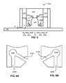
- FIG. 1 is a cross sectional diagram of a linear deposition device, according to one embodiment.
- FIG. 2 is a perspective view of a linear deposition device, according to one embodiment.
- FIG. 3 is a perspective view of a rotating deposition device, according to one embodiment.
- FIG. 4 is a diagram illustrating an injector according to one embodiment.
- FIG. 5 is a cross sectional diagram illustrating the injector taken along line A-B of FIG. 4 , according to one embodiment.
- FIGS. 6A and 6B are partially enlarged diagrams of the injector of FIG. 5 , according to one embodiment.
- FIG. 7 is a timing diagram illustrating sequence of materials injected through the injector, according to one embodiment.
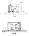
- FIG. 8A is a diagram illustrating flow of gas in the injector during the injection of source precursor, according to one embodiment.
- FIG. 8B is a diagram illustrating flow of gas in the injector during the injection of reactant precursor, according to one embodiment.
- FIGS. 9A through 9E are diagrams illustrating molecules deposited on a substrate, according to one embodiment.
- FIGS. 10A through 10C are diagrams illustrating materials deposited on the substrate depending on the speed of the substrate relative to the speed of gas switching, according to one embodiment.
- FIGS. 11A and 11B are cross sectional diagrams illustrating the injector according to another embodiment.
- FIG. 12 is a flowchart illustrating a process of performing atomic layer depositing using a combined injector, according to one embodiment.
- Embodiments relate to performing atomic layer deposition (ALD) using a combined injector that sequentially injects source precursor and reactant precursor onto a substrate.
- the source precursor is injected into the injector via a first channel, injected onto the substrate, and then discharged through a first exhaust portion.
- the reactant precursor is then injected into the injector via a second channel separate from the first channel, injected onto the substrate, and then discharged through a second exhaust portion separate from the first exhaust portion.
- a purge gas may be injected into the injector and discharged to remove any source precursor or reactant precursor remaining in paths from the first or second channel to the first or second exhaust portion.
- FIG. 1 is a cross sectional diagram of a linear deposition device 100 , according to one embodiment.
- FIG. 2 is a perspective view of the linear deposition device 100 (without chamber walls to facilitate explanation), according to one embodiment.
- the linear deposition device 100 may include, among other components, a support pillar 118 , the process chamber 110 and one or more reactors 136 .
- the reactors 136 may include one or more of injectors and radical reactors. Each of the injectors injects source precursors, reactant precursors, purge gases or a combination of these materials onto the substrate 120 .
- the process chamber enclosed by the walls may be maintained in a vacuum state to prevent contaminants from affecting the deposition process.
- the process chamber 110 contains a susceptor 128 which receives a substrate 120 .
- the susceptor 128 is placed on a support plate 124 for a sliding movement.
- the support plate 124 may include a temperature controller (e.g., a heater or a cooler) to control the temperature of the substrate 120 .
- the linear deposition device 100 may also include lift pins that facilitate loading of the substrate 120 onto the susceptor 128 or dismounting of the substrate 120 from the susceptor 128 .
- the susceptor 128 is secured to brackets 210 that moves across an extended bar 138 with screws formed thereon.
- the brackets 210 have corresponding screws formed in their holes receiving the extended bar 138 .
- the extended bar 138 is secured to a spindle of a motor 114 , and hence, the extended bar 138 rotates as the spindle of the motor 114 rotates.
- the rotation of the extended bar 138 causes the brackets 210 (and therefore the susceptor 128 ) to make a linear movement on the support plate 124 .
- the speed and direction of the linear movement of the susceptor 128 can be controlled.
- a motor 114 and the extended bar 138 is merely an example of a mechanism for moving the susceptor 128 .
- Various other ways of moving the susceptor 128 e.g., use of gears and pinion at the bottom, top or side of the susceptor 128 ).
- the susceptor 128 may remain stationary and the reactors 136 may be moved.
- FIG. 3 is a perspective view of a rotating deposition device 300 , according to one embodiment.
- the rotating deposition device 300 may be used to perform the deposition process according to another embodiment.
- the rotating deposition device 300 may include, among other components, reactors 320 , 334 , 364 , 368 , a susceptor 318 , and a container 324 enclosing these components.
- the susceptor 318 secures the substrates 314 in place.
- the reactors 320 , 334 , 364 , 368 are placed above the substrates 314 and the susceptor 318 . Either the susceptor 318 or the reactors 320 , 334 , 364 , 368 rotate to subject the substrates 314 to different processes.
- One or more of the reactors 320 , 334 , 364 , 368 are connected to gas pipes (not shown) to provide source precursor, reactor precursor, purge gas and/or other materials.
- the materials provided by the gas pipes may be (i) injected onto the substrate 314 directly by the reactors 320 , 334 , 364 , 368 , (ii) after mixing in a chamber inside the reactors 320 , 334 , 364 , 368 , or (iii) after conversion into radicals by plasma generated within the reactors 320 , 334 , 364 , 368 .
- the redundant materials may be exhausted through outlets 330 , 338 .
- Embodiments as described herein may be use in the linear deposition device 100 , the rotating deposition device 300 or other types of deposition device. Taking the examples of the linear deposition device 100 and the rotating deposition device 300 , the substrate 120 (or 314 ) may undergo different sequences of processes by moving the substrate 120 (or 314 ) relative to the reactors in one direction and then in an opposite direction.
- FIG. 4 is a diagram illustrating an injector 136 A according to one embodiment.
- the injector 136 A has a body 410 that is connected to discharge pipes 412 A, 412 B.
- a plurality of channels, holes or slits and a reactor chamber are formed in the body 410 to inject source precursor, reactant precursor and purge gas onto the substrate 120 .
- the injector 136 A includes mechanisms for routing excess source precursor and excess reactant precursor to different exhaust portions (refer to FIG. 5 ) that are connected to the discharge pipes 412 A, 412 B.
- each of the discharge pipes 412 A, 412 B carries one of the excess source precursor or the excess reactant precursor but not both precursors, as described below in detail with reference to FIG. 5 .
- the excess source precursor and the excess reactant precursor herein refer to source precursor and reactant precursor remaining after these materials are injected on the substrate 120 .
- the mechanism for routing the excess source precursor or the excess reactant precursor may include, among others, a gas injection channels in combination with slits or holes, and a mechanical shutter mechanism for closing a path to the discharge pipe 412 A or 412 B. Embodiments for such mechanisms are described below in detail with reference to FIGS. 6A , 6 B, 11 A and 11 B. However, other embodiments may use different ways to close the path to the discharge pipe 412 A or 412 B.
- the injector 136 A advantageously enables deposition of layers 420 without moving the substrate 120 .
- the substrate 120 is moved horizontally (e.g., to the right or the left in FIG. 4 ) to perform ALD on different parts of the substrate 120 .
- the ALD may be performed only on select portions of the substrate 120 (instead of an entire surface of the substrate 120 ), as described below in detail with reference to FIG. 10A .
- FIG. 5 is a cross sectional diagram illustrating the injector 136 A taken along line A-B of FIG. 4 , according to one embodiment.
- exhaust portions 510 , 514 , gas channels 522 A, 522 B, slits or holes 524 A, 524 B, a reaction chamber 520 , and purge gas channels 526 A, 526 B are formed.
- source precursor is injected into the reaction chamber 520 via the gas channel 522 A and slits/holes 524 A.
- a reactant precursor is also injected into the reaction chamber 520 via the gas channels 522 B and slits/holes 524 B. Below the reaction chamber 520 , the source precursor or the reactant precursor comes into contact with the substrate 120 .
- the source precursor and the reactant precursor are injected into the reaction chamber 520 sequentially with purge gases optionally cleaning out the reaction chamber 520 after each injection of the source precursor or the reactant precursor. In this way, reaction of the source precursor and the reactant precursor are prevented from occurring in the interior of the injector 136 A.
- the reaction of the source precursor and the reactant precursor within the injector 136 A may generate particles that block pathways or become contaminant for other processes.
- the source precursor and the reactant precursor travel via different routes except for the reaction chamber 520 to avoid undesirable interactions of the source precursor and the reactant within the injector 136 A.
- Inert gas may be injected towards the substrate 120 via the purge gas channels 526 A, 526 B.
- the amount of gas injected into each of the purge gas channels 526 A, 526 B is varied depending on whether the source precursor or the reactant precursor is being injected into the reaction chamber 520 , as described below in detail with reference to FIGS. 8A and 8B .
- the excess source precursor or the excess reactant precursor is routed to the exhaust portion 510 or 514 .
- the substrate 120 is exposed to the source precursor and the reactant precursor in a reaction zone R 1 .
- a layer of the source precursor or the reactant precursor is deposited on the substrate 120 in constriction zones R 2 A, R 2 B.
- the excess source precursor or the reactant precursor moves at a higher speed cue to a gap Z 2 compared to the reaction zone R 1 , and thereby removal of physisorbed source precursor or reactant precursor from the surface of the substrate 120 is facilitated. More complete removal of the physisorbed source precursor or the reactant precursor is achieved by purge gas injected after the injection of the source precursor or the reactant precursor.
- purge gas is injected into the reaction chamber 520 and discharged via the exhaust portion 510 , 514 to clear the reaction chamber 520 of the source precursor or the reactant precursor. Since the precursor molecules are discharged via the exhaust portions 510 , 514 , the source precursor or the reactant precursor do not become absorbed in the substrate 120 in exhaust zones R 3 A, R 3 B.
- FIGS. 6A and 6B are partially enlarged diagrams illustrating purge gas injection mechanism for routing the excess source precursor and the excess reactant precursor to the exhaust portions 510 , 514 , according to one embodiment.
- FIG. 6A shows the purge gas channel 526 A and perforations (e.g., slits or holes) 610 A, 620 A connected to the purge gas channel 526 A.
- perforations e.g., slits or holes
- FIG. 6A shows the purge gas channel 526 A and perforations (e.g., slits or holes) 610 A, 620 A connected to the purge gas channel 526 A.
- a smaller amount of purge gas (or no purge gas) is injected into the purge gas channels 526 , and hence, a flow of gas towards the exhaust portion 514 is formed.
- the remaining purge gas provided into the purge gas channels 526 A flows downwards via 620 A, forming a purge gas curtain that prevents the gas in the reaction chamber 520 from entering the exhaust portion 510 .
- the holes/slits 524 A for injecting the source precursor into the reactor chamber 520 is slanted towards the restriction zone R 2 B. Since the source precursor is injected towards the restriction zone R 2 B, the source precursor will tend to discharge via the exhaust portion 514 even absent the purge gas injected via the purge gas channels 526 A. By the combined action of the purge gas injected via the purge gas channel 526 A and the orientation of the holes/slits 524 A, most of the source precursor is discharged via the exhaust portion 514 .
- FIG. 6B shows the purge gas channel 526 B and perforations (slits or holes) 610 B, 620 B connected to the purge gas channels 526 B.
- the structure of the purge gas channel 526 B and slits or holes 610 B, 620 B mirrors the structure of the purge gas channel 526 A and slits or holes 610 A, 620 A.
- the principle of pushing the gas in the reaction chamber 520 to the exhaust portion 510 by the purge gas injected into the channel 526 B is the same as the explanation on injection of the purge gas into the channels 526 A.
- Part of the purge gas provided into the purge gas channels 526 B flows downwards via 620 B, forming a purge gas curtain that prevents the gas in the reaction chamber 520 from entering the exhaust portion 514 .
- the holes/slits 524 B is also slanted toward the restriction zone R 2 A to facilitate the discharge of the excess reactant precursor via the exhaust portion 510 .
- FIG. 7 is a timing diagram illustrating the sequence of materials injected through the injector, according to one embodiment.
- the embodiment of FIG. 7 relates to using Trimethylaluminium (TMA) as the source precursor and ozone (O 3 ) as the reactant precursor to form one or more layers of Al 2 O 3 on the substrate 120 .
- TMA Trimethylaluminium
- O 3 ozone
- two cycles of the same processes are repeated to deposit two layers of Al 2 O 3 on the substrate 120 .
- the source precursor (TMA) is injected into the reaction chamber 520 via the channel 522 A and the slits or holes 524 A, and then discharged via the exhaust portion 514 , as described below in detail with reference to FIG. 8A .
- the reactant precursor ozone
- the Argon gas is injected into the purge gas channels 526 A, 526 B (the amount of Argon gas injected into the purge gas channel 526 A is greater than the amount of Argon gas injected into the purge gas channel 526 B).
- FIG. 8A is a diagram illustrating flow of gas in the injector 136 A during the injection of source precursor, according to one embodiment.
- the excess source precursor 810 is discharged via the exhaust portion 514 due to the higher volume of Argon gas injected via the purge gas channel 526 A compared to the purge gas channel 526 B. Part of the Argon gas 814 injected via the purge gas channel 526 A is discharged via the exhaust portion 510 .
- the supply of the source precursor (TMA) is stopped during time period t 2 . Instead, Argon gas is injected into the reaction chamber 520 via the channel 522 A and the slits or holes 524 A. Argon gas discharges the source precursor remaining in the reaction chamber 520 through the exhaust portion 514 . Moreover, during this period, Argon supplied via the channel 520 (in conjunction with Argon supplied via the purge gas channels 526 A, 526 B) removes source precursor molecules physisorbed on the surface of the substrate 520 .
- FIG. 8B is a diagram illustrating flow of gas in the injector 136 A during the injection of reactant precursor, according to one embodiment.
- the excess source precursor 820 is discharged via the exhaust portion 510 due to the higher volume of Argon gas injected via the purge gas channel 526 B compared to the purge gas channel 526 A.
- Part of the Argon gas 824 injected via the purge gas channel 526 B is discharged via the exhaust portion 514 .
- the supply of the reactant precursor is stopped during time period t 4 .
- Argon gas is injected into the reaction chamber 520 via the channel 522 B and the slits or holes 524 B.
- Argon gas discharges the reactant precursor remaining in the reaction chamber 520 through the exhaust portion 510 .
- Argon supplied via the channel 520 in conjunction with Argon supplied via the purge gas channels 526 A, 526 B) removes source precursor molecules physisorbed on the surface of the substrate 520 .
- the end of period t 4 concludes the first cycle.
- the second cycle is repeated to deposit a second layer of Al 2 O 3 .
- FIGS. 9A through 9E are diagrams illustrating molecules deposited on a substrate, according to one embodiment.
- FIG. 9A illustrates TMA molecules deposited on the substrate 120 after period t 1 of FIG. 7 .
- some physisorbed TMA molecules (layers of TMA molecules above the first layer) remain on the reaction zone R 1 and the constriction zone R 2 B of the substrate 120 .
- purge gas Argon gas
- physisorbed TMA molecules are removed from the surface of the substrate 120 .
- a single layer of chemisorbed TMA molecules remains on the substrate 120 , as shown in FIG. 9B .
- the reactant precursor (ozone) is injected onto the substrate 120 .
- the reactant precursor reacts with the chemisorbed source precursor in the reaction zone R 1 of the substrate 120 and forms a single layer of Al 2 O 3 .
- a layer of H 2 O, OH or O* molecules is deposited on the surface of the substrate and on the layer of Al 2 O 3 in the reaction zone R 1 and the constriction zone R 2 A, as shown in FIG. 9C .
- purge gas Ar
- physisorbed H 2 O, OH or O* molecules are removed from the surface of the substrate 120 in the reaction zone R 1 .
- a single layer of chemisorbed TMA molecules remains on the substrate 120 in the reaction zone R 1 .
- a single layer of chemisorbed H 2 O, OH or O* molecules also remains in the constriction zone R 2 A while a single layer of chemisorbed TMA molecules also remains in the constriction zone R 2 B of the substrate 120 .
- FIG. 9E illustrates subjecting the substrate 120 to four cycles of process as described above with reference to FIGS. 9A through 9D .
- four layer of Al 2 O 3 is formed on the reaction zone R 1 of the substrate 120 while a single layer of H 2 O, OH or O* molecules remains in the constriction zone R 2 A of the substrate and a single layer of TMA molecules remains in the constriction zone R 2 B of the substrate 120 .
- the injector 136 A allows multiple layers of Al 2 O 3 to be deposited on the same location of the substrate 120 without moving the substrate 120 .
- the substrate 120 should be moved horizontally to expose the same area of the substrate 120 to different precursor molecules.
- the injector 136 A enables performing of ALD on a certain region of the substrate 120 without moving the substrate 120 since the same injector 136 A injects both the source precursor and the reactant precursor.
- the injector 136 A may reduce the reciprocation or the rotation of the substrate 120 to deposit the materials on the substrate 120 as well as allowing more localized deposition of materials on the substrate 120 . Further, by removing additional injectors, the cost of the deposition apparatus can be reduced.
- FIGS. 10A through 10C are diagrams illustrating layout of materials deposited on the substrate depending on the speed of the substrate relative to the speed of gas switching, according to one embodiment.
- FIG. 10A illustrates an example where the moving of the substrate 120 is not correctly timed to form an atomic layer on the substrate 120 . Consequently, source precursor molecules are deposited in region 130 for a width of L 1 followed by a region where no molecules are deposited for a width of L 2 followed by a region 122 where reactant precursor molecules are deposited.
- FIG. 10B illustrates an example where the moving of the substrate 120 is arranged so that the source precursor and the reactant precursor react within only on regions 126 of the substrate 120 marked by black boxes. The remaining regions 124 , 128 of the substrate 120 are covered with either the source precursor molecules or the reactant precursor molecules.
- FIG. 10C illustrates an example where substantially the entire surface 142 of the substrate 120 is subject to the source precursor and then the reactant precursor.
- the substrate 120 is moved only after a reaction zone R 1 of the substrate 120 is subject to the source precursor and the reactant precursor.
- FIGS. 11A and 11B are cross sectional diagrams illustrating an injector 136 B, according to another embodiment.
- the injector 136 B includes a set of shutters 1134 A, 1134 B that are lowered to close certain paths and route the excess source precursor or the reactant precursor to the exhaust portion 1154 or the exhaust portion 1158 .
- Motors or other link structures for raising or lowering the shutters 1134 A, 1134 B are also provided but not shown in FIGS. 11A and 11B .
- the left shutter 1134 A is lowered.
- the gap Z 2 between the substrate 120 and the shutter 1134 A becomes smaller, and hence, practically closing a path from the reaction chamber 1130 to the exhaust portion 1154 .
- only a small amount of source precursor molecules (if any) pass below the shutter 1134 and discharge via the exhaust portion 1154 .
- the majority of source precursor molecules travels below the raised shutter 1134 B (having a gap Z 3 with respect to the substrate 120 ), and discharges via the exhaust portion 1158 .
- a purge gas may be injected into the reaction chamber 1130 via the channel 1114 A and holes or slits 1118 A to discharge the source precursor from the reaction chamber 1130 .
- the left shutter 1134 A is raised while the right shutter 1134 B is lowered.
- the lowering of the right shutter 1134 practically closes a path from the reactor chamber 1130 to the exhaust portion 1158 , causing the excess reactant precursor to discharge via the exhaust portion 1154 .
- a purge gas may be injected into the reaction chamber 1130 via the channel 1114 B and holes or slits 1118 B to discharge the reactant precursor from the reaction chamber 1130 .
- the source precursor and the reactant precursor do not react in areas other than on the surface of the substrate. In this way, particles are not formed in the interior of the injector even when a combined injector is used to inject both the source precursor and the reactant precursor onto the substrate.
- FIG. 12 is a flowchart illustrating the process of performing ALD using a combined injector 136 A, 136 B, according to one embodiment.
- the source precursor provided into a reaction chamber via a first channel e.g., channel 522 A, 1118 A
- the excess source precursor is then routed 1220 to a first exhaust portion (e.g., the exhaust portion 514 , 1158 ) by a routing mechanism.
- the routing mechanism may include a purge gas channel and slits or holes connected to the purge gas channels (as described above with reference to FIGS. 6A and 6B ) or a set of shutters (as described above with reference to FIGS. 11A and 11B ).
- Purge gas is then injected 1230 into the reaction chamber via the first channel to discharge the source precursor from the reaction chamber.
- the reactant precursor is then provided into the reaction chamber via a second channel (e.g., channel 522 B, 1118 B).
- the reactant precursor is injected 1240 onto the substrate 120 .
- the excess reactant precursor is then routed 1250 to a second exhaust portion (e.g., the exhaust portion 510 , 1154 ) by a routing mechanism.
- Purge gas is then injected 1260 into the reaction chamber via the second channel to discharge the reactant precursor from the reaction chamber.
- the process determines 1270 if the layer of material deposited on the substrate 120 is of a desired thickness. If the thickness of the deposited material is of a desired thickness, then the process terminates. If the thickness of the deposited material is thinner than desired, the process returns to injecting 1210 the source precursor and repeats the subsequent steps.
Abstract
Description
Claims (11)
Priority Applications (4)
| Application Number | Priority Date | Filing Date | Title |
|---|---|---|---|
| US13/368,265 US8840958B2 (en) | 2011-02-14 | 2012-02-07 | Combined injection module for sequentially injecting source precursor and reactant precursor |
| PCT/US2012/024451 WO2012112373A1 (en) | 2011-02-14 | 2012-02-09 | Combined injection module for sequentially injecting source precursor and reactant precursor |
| KR1020137024193A KR101495465B1 (en) | 2011-02-14 | 2012-02-09 | Combined injection module for sequentially injecting source precursor and reactant precursor |
| TW101104784A TWI519670B (en) | 2011-02-14 | 2012-02-14 | Combined injection module for sequentially injecting source precursor and reactant precursor |
Applications Claiming Priority (2)
| Application Number | Priority Date | Filing Date | Title |
|---|---|---|---|
| US201161442778P | 2011-02-14 | 2011-02-14 | |
| US13/368,265 US8840958B2 (en) | 2011-02-14 | 2012-02-07 | Combined injection module for sequentially injecting source precursor and reactant precursor |
Publications (2)
| Publication Number | Publication Date |
|---|---|
| US20120207926A1 US20120207926A1 (en) | 2012-08-16 |
| US8840958B2 true US8840958B2 (en) | 2014-09-23 |
Family
ID=46637089
Family Applications (1)
| Application Number | Title | Priority Date | Filing Date |
|---|---|---|---|
| US13/368,265 Expired - Fee Related US8840958B2 (en) | 2011-02-14 | 2012-02-07 | Combined injection module for sequentially injecting source precursor and reactant precursor |
Country Status (4)
| Country | Link |
|---|---|
| US (1) | US8840958B2 (en) |
| KR (1) | KR101495465B1 (en) |
| TW (1) | TWI519670B (en) |
| WO (1) | WO2012112373A1 (en) |
Cited By (2)
| Publication number | Priority date | Publication date | Assignee | Title |
|---|---|---|---|---|
| US20120247390A1 (en) * | 2009-09-17 | 2012-10-04 | Tokyo Electron Limited | Film formation apparatus |
| DE102017204214A1 (en) | 2016-03-14 | 2017-09-14 | Veeco Instruments Inc. | GAS CONCENTRATION SENSORS AND SYSTEMS |
Families Citing this family (9)
| Publication number | Priority date | Publication date | Assignee | Title |
|---|---|---|---|---|
| US8333839B2 (en) * | 2007-12-27 | 2012-12-18 | Synos Technology, Inc. | Vapor deposition reactor |
| US8470718B2 (en) * | 2008-08-13 | 2013-06-25 | Synos Technology, Inc. | Vapor deposition reactor for forming thin film |
| US8758512B2 (en) * | 2009-06-08 | 2014-06-24 | Veeco Ald Inc. | Vapor deposition reactor and method for forming thin film |
| US20110076421A1 (en) * | 2009-09-30 | 2011-03-31 | Synos Technology, Inc. | Vapor deposition reactor for forming thin film on curved surface |
| FI126043B (en) | 2013-06-27 | 2016-06-15 | Beneq Oy | Method and apparatus for coating the surface of a substrate |
| KR102173047B1 (en) * | 2013-10-10 | 2020-11-03 | 삼성디스플레이 주식회사 | Vapor deposition apparatus |
| JP6640781B2 (en) * | 2017-03-23 | 2020-02-05 | キオクシア株式会社 | Semiconductor manufacturing equipment |
| US10981193B2 (en) * | 2017-04-05 | 2021-04-20 | Nova Engineering Films, Inc. | Depositing of material by spraying precursor using supercritical fluid |
| US11588140B2 (en) * | 2018-01-12 | 2023-02-21 | Universal Display Corporation | Organic vapor jet print head for depositing thin film features with high thickness uniformity |
Citations (114)
| Publication number | Priority date | Publication date | Assignee | Title |
|---|---|---|---|---|
| US4293326A (en) | 1978-07-20 | 1981-10-06 | Bfg Glassgroup | Glass coating |
| JPS6281018A (en) | 1985-10-04 | 1987-04-14 | Hitachi Ltd | Normal pressure cvd device |
| JPH0196924A (en) | 1987-10-09 | 1989-04-14 | Matsushita Electric Ind Co Ltd | Film formation by thermochemical vapor deposition process |
| US4834020A (en) | 1987-12-04 | 1989-05-30 | Watkins-Johnson Company | Atmospheric pressure chemical vapor deposition apparatus |
| JPH01223724A (en) | 1988-03-02 | 1989-09-06 | Mitsubishi Electric Corp | Chemical vapor growth device |
| US4891247A (en) | 1986-09-15 | 1990-01-02 | Watkins-Johnson Company | Process for borosilicate glass films for multilevel metallization structures in semiconductor devices |
| JPH02187018A (en) | 1989-01-13 | 1990-07-23 | Mitsubishi Electric Corp | Chemical vapor phase deposition device |
| US5063951A (en) | 1990-07-19 | 1991-11-12 | International Business Machines Corporation | Fluid treatment device |
| JPH0492414A (en) | 1990-08-08 | 1992-03-25 | Mitsubishi Electric Corp | Thin film formation device |
| US5122391A (en) | 1991-03-13 | 1992-06-16 | Watkins-Johnson Company | Method for producing highly conductive and transparent films of tin and fluorine doped indium oxide by APCVD |
| US5136975A (en) | 1990-06-21 | 1992-08-11 | Watkins-Johnson Company | Injector and method for delivering gaseous chemicals to a surface |
| EP0499524A1 (en) | 1991-02-13 | 1992-08-19 | Saint-Gobain Vitrage International | Asymmetrical gas feeding nozzle for coating a glass ribbon by pyrolysis of a gas mixture |
| US5275668A (en) | 1990-08-20 | 1994-01-04 | Dell Joseph G | Hydro impact medical and dental instruments washer |
| US5482557A (en) | 1986-01-14 | 1996-01-09 | Canon Kabushiki Kaisha | Device for forming deposited film |
| FR2736632A1 (en) | 1995-07-12 | 1997-01-17 | Saint Gobain Vitrage | GLAZING WITH CONDUCTIVE AND / OR LOW-EMISSIVE LAYER |
| JPH0964000A (en) | 1995-08-18 | 1997-03-07 | Matsushita Electric Ind Co Ltd | Dry cleaning device |
| US5683516A (en) | 1994-07-18 | 1997-11-04 | Watkins-Johnson Co. | Single body injector and method for delivering gases to a surface |
| US5725668A (en) | 1995-09-06 | 1998-03-10 | International Business Machines Corporation | Expandable fluid treatment device for tublar surface treatments |
| US5879459A (en) | 1997-08-29 | 1999-03-09 | Genus, Inc. | Vertically-stacked process reactor and cluster tool system for atomic layer deposition |
| WO1999039144A1 (en) | 1998-02-02 | 1999-08-05 | Silicon Valley Group Thermal Systems, Llc. | Wafer carrier and semiconductor apparatus for processing a semiconductor substrate |
| JPH11285882A (en) | 1998-03-31 | 1999-10-19 | Amada Co Ltd | Double structure nozzle with control function |
| US6022414A (en) | 1994-07-18 | 2000-02-08 | Semiconductor Equipment Group, Llc | Single body injector and method for delivering gases to a surface |
| US6079353A (en) | 1998-03-28 | 2000-06-27 | Quester Technology, Inc. | Chamber for reducing contamination during chemical vapor deposition |
| US6083355A (en) | 1997-07-14 | 2000-07-04 | The University Of Tennessee Research Corporation | Electrodes for plasma treater systems |
| US6143077A (en) | 1996-08-13 | 2000-11-07 | Anelva Corporation | Chemical vapor deposition apparatus |
| US6195504B1 (en) | 1996-11-20 | 2001-02-27 | Ebara Corporation | Liquid feed vaporization system and gas injection device |
| US6200389B1 (en) | 1994-07-18 | 2001-03-13 | Silicon Valley Group Thermal Systems Llc | Single body injector and deposition chamber |
| US6206972B1 (en) | 1999-07-08 | 2001-03-27 | Genus, Inc. | Method and apparatus for providing uniform gas delivery to substrates in CVD and PECVD processes |
| JP2001357780A (en) | 2000-06-16 | 2001-12-26 | Matsushita Electric Ind Co Ltd | Manufacturing method and manufacturing device of plasma display panel |
| US6416822B1 (en) | 2000-12-06 | 2002-07-09 | Angstrom Systems, Inc. | Continuous method for depositing a film by modulated ion-induced atomic layer deposition (MII-ALD) |
| US6435428B2 (en) | 2000-02-16 | 2002-08-20 | Apex Co., Ltd. | Showerhead apparatus for radical-assisted deposition |
| KR20020078804A (en) | 2001-04-10 | 2002-10-19 | 주식회사 싸일렌테크놀로지 | Atmosphere pressure plasma generator |
| KR20020083564A (en) | 2001-04-27 | 2002-11-04 | 주식회사 엘지이아이 | Multiplasma producer |
| JP2002339075A (en) | 2001-05-17 | 2002-11-27 | Konica Corp | Surface treatment method for long material and optical film produced by the method |
| US6539891B1 (en) | 1999-06-19 | 2003-04-01 | Genitech, Inc. | Chemical deposition reactor and method of forming a thin film using the same |
| US20030072881A1 (en) | 2001-06-11 | 2003-04-17 | General Electric Company | Apparatus and method for large area chemical vapor deposition using multiple expanding thermal plasma generators |
| US6569501B2 (en) | 2000-12-06 | 2003-05-27 | Angstron Systems, Inc. | Sequential method for depositing a film by modulated ion-induced atomic layer deposition (MII-ALD) |
| JP2003174019A (en) | 2001-12-05 | 2003-06-20 | Sumitomo Precision Prod Co Ltd | Ozone treatment device |
| US6634314B2 (en) | 2000-08-09 | 2003-10-21 | Jusung Engineering Co., Ltd. | Atomic layer deposition method and semiconductor device fabricating apparatus having rotatable gas injectors |
| US20030198587A1 (en) | 1999-02-12 | 2003-10-23 | Gelest, Inc. | Method for low-temperature organic chemical vapor deposition of tungsten nitride, tungsten nitride films and tungsten nitride diffusion barriers for computer interconnect metallization |
| KR20030086056A (en) | 2002-05-03 | 2003-11-07 | 주식회사 무한 | Atomic layer deposition apparatus for manufacturing Semiconductor device and atomic layer deposition method thereof |
| JP2003324070A (en) | 2002-04-30 | 2003-11-14 | Suzuki Motor Corp | Method and device of manufacturing thin film |
| US6656284B1 (en) | 2002-06-28 | 2003-12-02 | Jusung Engineering Co., Ltd. | Semiconductor device manufacturing apparatus having rotatable gas injector and thin film deposition method using the same |
| JP2004010949A (en) | 2002-06-05 | 2004-01-15 | Seiko Epson Corp | Apparatus and method for forming film |
| KR20040016779A (en) | 2002-08-17 | 2004-02-25 | 삼성전자주식회사 | Method of forming oxide layer using atomic layer deposition method and method of forming capacitor of semiconductor device using the same |
| US20040067641A1 (en) | 2002-10-02 | 2004-04-08 | Applied Materials, Inc. | Gas distribution system for cyclical layer deposition |
| US20040129212A1 (en) | 2002-05-20 | 2004-07-08 | Gadgil Pradad N. | Apparatus and method for delivery of reactive chemical precursors to the surface to be treated |
| US6812157B1 (en) | 1999-06-24 | 2004-11-02 | Prasad Narhar Gadgil | Apparatus for atomic layer chemical vapor deposition |
| US20040216668A1 (en) * | 2003-04-29 | 2004-11-04 | Sven Lindfors | Showerhead assembly and ALD methods |
| US6824816B2 (en) | 2002-01-29 | 2004-11-30 | Asm International N.V. | Process for producing metal thin films by ALD |
| US20040265195A1 (en) | 2003-06-25 | 2004-12-30 | Jusung Engineering Co., Ltd. | Gas injector for use in semiconductor fabricating apparatus |
| KR20050015931A (en) | 2003-08-05 | 2005-02-21 | 주성엔지니어링(주) | Chamber and showerhead for uniform layer deposition |
| JP2005089781A (en) | 2003-09-12 | 2005-04-07 | Mitsui Eng & Shipbuild Co Ltd | Thin film deposition system |
| US20050084610A1 (en) * | 2002-08-13 | 2005-04-21 | Selitser Simon I. | Atmospheric pressure molecular layer CVD |
| JP2005116898A (en) | 2003-10-09 | 2005-04-28 | Sekisui Chem Co Ltd | Plasma processing apparatus |
| US20050092247A1 (en) | 2003-08-29 | 2005-05-05 | Schmidt Ryan M. | Gas mixer and manifold assembly for ALD reactor |
| US6890386B2 (en) | 2001-07-13 | 2005-05-10 | Aviza Technology, Inc. | Modular injector and exhaust assembly |
| US6926572B2 (en) | 2002-01-25 | 2005-08-09 | Electronics And Telecommunications Research Institute | Flat panel display device and method of forming passivation film in the flat panel display device |
| US6972055B2 (en) | 2003-03-28 | 2005-12-06 | Finens Corporation | Continuous flow deposition system |
| WO2006054854A1 (en) | 2004-11-18 | 2006-05-26 | Ips Ltd. | A method for depositing thin film using ald |
| US7087119B2 (en) | 2002-03-05 | 2006-08-08 | Micron Technology, Inc. | Atomic layer deposition with point of use generated reactive gas species |
| US20060183301A1 (en) | 2005-02-16 | 2006-08-17 | Seung-Jin Yeom | Method for forming thin film |
| US7118779B2 (en) | 2003-05-09 | 2006-10-10 | Asm America, Inc. | Reactor surface passivation through chemical deactivation |
| KR20060117607A (en) | 2005-05-13 | 2006-11-17 | 오재응 | Vapor deposition reactor |
| KR100673211B1 (en) | 2000-06-30 | 2007-01-22 | 주식회사 하이닉스반도체 | Showerhead |
| US20070095286A1 (en) | 2004-12-16 | 2007-05-03 | Yong-Ku Baek | Apparatus and method for thin film deposition |
| KR20070076955A (en) | 2006-01-20 | 2007-07-25 | 주성엔지니어링(주) | Method of forming thin film |
| WO2007106076A2 (en) | 2006-03-03 | 2007-09-20 | Prasad Gadgil | Apparatus and method for large area multi-layer atomic layer chemical vapor processing of thin films |
| KR20070096770A (en) | 2006-03-23 | 2007-10-02 | 삼성전자주식회사 | Method of forming carbon polymer film using plasma chemical vapor deposition |
| JP2007266093A (en) | 2006-03-27 | 2007-10-11 | Mitsubishi Heavy Ind Ltd | Production device for optoelectric transducer, and manufacturing method for the optoelectric transducer |
| KR20070101127A (en) | 2006-04-11 | 2007-10-16 | 고이께 산소 고교 가부시끼가이샤 | Plasma torch |
| KR20070101360A (en) | 2005-01-28 | 2007-10-16 | 테크나 플라즈마 시스템 인코포레이티드 | Induction plasma synthesis of nanopowders |
| KR100791677B1 (en) | 2006-10-27 | 2008-01-03 | 동부일렉트로닉스 주식회사 | High density plasma chemical vapor deposition apparatus for semiconductor device manufacturing |
| JP2008108895A (en) | 2006-10-25 | 2008-05-08 | Sekisui Chem Co Ltd | Surface processing method and apparatus thereof |
| US20080124945A1 (en) * | 2005-02-17 | 2008-05-29 | Hitachi Kokusa Electric Inc. | Production Method for Semiconductor Device and Substrate Processing Apparatus |
| US7384680B2 (en) | 1997-07-21 | 2008-06-10 | Nanogram Corporation | Nanoparticle-based power coatings and corresponding structures |
| KR100840897B1 (en) | 2007-02-26 | 2008-06-24 | 주식회사 테스 | Assembly for supporting substrate and apparatus for treating substrate and method for treating substrate |
| KR20080067042A (en) | 2007-01-15 | 2008-07-18 | 최대규 | Inductively coupled plasma reactor with core cover |
| US20080260967A1 (en) | 2007-04-17 | 2008-10-23 | Hyungsuk Alexander Yoon | Apparatus and method for integrated surface treatment and film deposition |
| US20080260940A1 (en) | 2007-04-17 | 2008-10-23 | Hyungsuk Alexander Yoon | Apparatus and method for integrated surface treatment and deposition for copper interconnect |
| WO2008130369A1 (en) | 2007-04-17 | 2008-10-30 | Lam Research Corporation | Apparatus and method for atomic layer deposition |
| US20090017190A1 (en) | 2007-07-10 | 2009-01-15 | Veeco Instruments Inc. | Movable injectors in rotating disc gas reactors |
| US20090047775A1 (en) | 2007-08-17 | 2009-02-19 | Semiconductor Energy Laboratory Co., Ltd. | Method for manufacturing display device |
| US7494545B2 (en) | 2006-02-03 | 2009-02-24 | Applied Materials, Inc. | Epitaxial deposition process and apparatus |
| US20090068849A1 (en) | 2007-09-06 | 2009-03-12 | Rick Endo | Multi-region processing system and heads |
| US20090064932A1 (en) | 2007-08-31 | 2009-03-12 | Samsung Electronics Co., Ltd. | Apparatus for HDP-CVD and method of forming insulating layer using the same |
| US20090081885A1 (en) * | 2007-09-26 | 2009-03-26 | Levy David H | Deposition system for thin film formation |
| WO2009042147A1 (en) | 2007-09-26 | 2009-04-02 | Eastman Kodak Company | Process and deposition system for thin film formation with gas delivery head having spatial separation of reactive gases and movement of the substrate passed the delivery head |
| US20090098276A1 (en) | 2007-10-16 | 2009-04-16 | Applied Materials, Inc. | Multi-gas straight channel showerhead |
| US20090130858A1 (en) | 2007-01-08 | 2009-05-21 | Levy David H | Deposition system and method using a delivery head separated from a substrate by gas pressure |
| US20090165715A1 (en) * | 2007-12-27 | 2009-07-02 | Oh Jae-Eung | Vapor deposition reactor |
| US20100041213A1 (en) | 2008-08-13 | 2010-02-18 | Synos Technology, Inc. | Vapor Deposition Reactor For Forming Thin Film |
| US20100037820A1 (en) | 2008-08-13 | 2010-02-18 | Synos Technology, Inc. | Vapor Deposition Reactor |
| EP2159304A1 (en) | 2008-08-27 | 2010-03-03 | Nederlandse Organisatie voor toegepast- natuurwetenschappelijk onderzoek TNO | Apparatus and method for atomic layer deposition |
| US20100055347A1 (en) | 2008-08-29 | 2010-03-04 | Tokyo Electron Limited | Activated gas injector, film deposition apparatus, and film deposition method |
| US20100124618A1 (en) | 2008-11-14 | 2010-05-20 | Asm Japan K.K. | Method of Forming Insulation Film Using Plasma Treatment Cycles |
| US20100132615A1 (en) | 2008-12-02 | 2010-06-03 | Tokyo Electron Limited | Film deposition apparatus |
| US20100140802A1 (en) | 2007-06-04 | 2010-06-10 | Tokyo Electron Limited | Film forming method and film forming apparatus |
| US7754013B2 (en) | 2002-12-05 | 2010-07-13 | Asm International N.V. | Apparatus and method for atomic layer deposition on substrates |
| US20100221426A1 (en) | 2009-03-02 | 2010-09-02 | Fluens Corporation | Web Substrate Deposition System |
| US20100310771A1 (en) | 2009-06-08 | 2010-12-09 | Synos Technology, Inc. | Vapor deposition reactor and method for forming thin film |
| US20110005681A1 (en) * | 2009-07-08 | 2011-01-13 | Stephen Edward Savas | Plasma Generating Units for Processing a Substrate |
| US7914847B2 (en) | 2003-05-09 | 2011-03-29 | Asm America, Inc. | Reactor surface passivation through chemical deactivation |
| US20110076421A1 (en) | 2009-09-30 | 2011-03-31 | Synos Technology, Inc. | Vapor deposition reactor for forming thin film on curved surface |
| US7943527B2 (en) | 2008-05-30 | 2011-05-17 | The Board Of Trustees Of The University Of Illinois | Surface preparation for thin film growth by enhanced nucleation |
| US7981472B2 (en) | 2006-04-05 | 2011-07-19 | Aixtron, Inc. | Methods of providing uniform gas delivery to a reactor |
| EP2360293A1 (en) | 2010-02-11 | 2011-08-24 | Nederlandse Organisatie voor toegepast -natuurwetenschappelijk onderzoek TNO | Method and apparatus for depositing atomic layers on a substrate |
| US20120021252A1 (en) | 2010-07-22 | 2012-01-26 | Synos Technology, Inc. | Treating Surface of Substrate Using Inert Gas Plasma in Atomic Layer Deposition |
| US20120027953A1 (en) | 2010-07-28 | 2012-02-02 | Synos Technology, Inc. | Rotating Reactor Assembly for Depositing Film on Substrate |
| WO2012028776A1 (en) | 2010-08-30 | 2012-03-08 | Beneq Oy | Apparatus |
| US20120196050A1 (en) | 2009-07-30 | 2012-08-02 | Adrianus Johannes Petrus Maria Vermeer | Apparatus and method for atomic layer deposition |
| US20120225207A1 (en) | 2011-03-01 | 2012-09-06 | Applied Materials, Inc. | Apparatus and Process for Atomic Layer Deposition |
| US20120225206A1 (en) | 2011-03-01 | 2012-09-06 | Applied Materials, Inc. | Apparatus and Process for Atomic Layer Deposition |
| US20120225204A1 (en) | 2011-03-01 | 2012-09-06 | Applied Materials, Inc. | Apparatus and Process for Atomic Layer Deposition |
-
2012
- 2012-02-07 US US13/368,265 patent/US8840958B2/en not_active Expired - Fee Related
- 2012-02-09 WO PCT/US2012/024451 patent/WO2012112373A1/en active Application Filing
- 2012-02-09 KR KR1020137024193A patent/KR101495465B1/en not_active IP Right Cessation
- 2012-02-14 TW TW101104784A patent/TWI519670B/en not_active IP Right Cessation
Patent Citations (130)
| Publication number | Priority date | Publication date | Assignee | Title |
|---|---|---|---|---|
| US4293326A (en) | 1978-07-20 | 1981-10-06 | Bfg Glassgroup | Glass coating |
| JPS6281018A (en) | 1985-10-04 | 1987-04-14 | Hitachi Ltd | Normal pressure cvd device |
| US5482557A (en) | 1986-01-14 | 1996-01-09 | Canon Kabushiki Kaisha | Device for forming deposited film |
| US4891247A (en) | 1986-09-15 | 1990-01-02 | Watkins-Johnson Company | Process for borosilicate glass films for multilevel metallization structures in semiconductor devices |
| JPH0196924A (en) | 1987-10-09 | 1989-04-14 | Matsushita Electric Ind Co Ltd | Film formation by thermochemical vapor deposition process |
| US4834020A (en) | 1987-12-04 | 1989-05-30 | Watkins-Johnson Company | Atmospheric pressure chemical vapor deposition apparatus |
| JPH01223724A (en) | 1988-03-02 | 1989-09-06 | Mitsubishi Electric Corp | Chemical vapor growth device |
| JPH02187018A (en) | 1989-01-13 | 1990-07-23 | Mitsubishi Electric Corp | Chemical vapor phase deposition device |
| US5136975A (en) | 1990-06-21 | 1992-08-11 | Watkins-Johnson Company | Injector and method for delivering gaseous chemicals to a surface |
| US5063951A (en) | 1990-07-19 | 1991-11-12 | International Business Machines Corporation | Fluid treatment device |
| JPH0492414A (en) | 1990-08-08 | 1992-03-25 | Mitsubishi Electric Corp | Thin film formation device |
| US5275668A (en) | 1990-08-20 | 1994-01-04 | Dell Joseph G | Hydro impact medical and dental instruments washer |
| EP0499524A1 (en) | 1991-02-13 | 1992-08-19 | Saint-Gobain Vitrage International | Asymmetrical gas feeding nozzle for coating a glass ribbon by pyrolysis of a gas mixture |
| US5286295A (en) | 1991-02-13 | 1994-02-15 | Saint-Gobain Vitrage International | Nozzle with nonsymmetrical feed for the formation of a coating layer on a ribbon of glass, by pyrolysis of a gas mixture |
| US5122391A (en) | 1991-03-13 | 1992-06-16 | Watkins-Johnson Company | Method for producing highly conductive and transparent films of tin and fluorine doped indium oxide by APCVD |
| US6022414A (en) | 1994-07-18 | 2000-02-08 | Semiconductor Equipment Group, Llc | Single body injector and method for delivering gases to a surface |
| US5683516A (en) | 1994-07-18 | 1997-11-04 | Watkins-Johnson Co. | Single body injector and method for delivering gases to a surface |
| US6521048B2 (en) | 1994-07-18 | 2003-02-18 | Asml Us, Inc. | Single body injector and deposition chamber |
| US5935647A (en) | 1994-07-18 | 1999-08-10 | Wj Semiconductor Equipment Group, Inc. | Method of manufacturing an injector for chemical vapor deposition processing |
| US6200389B1 (en) | 1994-07-18 | 2001-03-13 | Silicon Valley Group Thermal Systems Llc | Single body injector and deposition chamber |
| JPH10507994A (en) | 1995-07-12 | 1998-08-04 | サン−ゴバン ビトラージュ | Flat glass containing conductive and / or low emissivity layer |
| CN1436602A (en) | 1995-07-12 | 2003-08-20 | 法国圣戈班玻璃厂 | Nozzle and its using method |
| FR2736632A1 (en) | 1995-07-12 | 1997-01-17 | Saint Gobain Vitrage | GLAZING WITH CONDUCTIVE AND / OR LOW-EMISSIVE LAYER |
| US6354109B1 (en) | 1995-07-12 | 2002-03-12 | Saint-Gobain Glass France | Process and apparatus for providing a film with a gradient |
| JPH0964000A (en) | 1995-08-18 | 1997-03-07 | Matsushita Electric Ind Co Ltd | Dry cleaning device |
| US5725668A (en) | 1995-09-06 | 1998-03-10 | International Business Machines Corporation | Expandable fluid treatment device for tublar surface treatments |
| US6143077A (en) | 1996-08-13 | 2000-11-07 | Anelva Corporation | Chemical vapor deposition apparatus |
| US6195504B1 (en) | 1996-11-20 | 2001-02-27 | Ebara Corporation | Liquid feed vaporization system and gas injection device |
| US6083355A (en) | 1997-07-14 | 2000-07-04 | The University Of Tennessee Research Corporation | Electrodes for plasma treater systems |
| US7384680B2 (en) | 1997-07-21 | 2008-06-10 | Nanogram Corporation | Nanoparticle-based power coatings and corresponding structures |
| US5879459A (en) | 1997-08-29 | 1999-03-09 | Genus, Inc. | Vertically-stacked process reactor and cluster tool system for atomic layer deposition |
| WO1999039144A1 (en) | 1998-02-02 | 1999-08-05 | Silicon Valley Group Thermal Systems, Llc. | Wafer carrier and semiconductor apparatus for processing a semiconductor substrate |
| KR20010040561A (en) | 1998-02-02 | 2001-05-15 | 실리콘 밸리 그룹 써어멀 시스템즈, 엘엘씨 | Wafer carrier and semiconductor apparatus for processing a semiconductor substrate |
| US6079353A (en) | 1998-03-28 | 2000-06-27 | Quester Technology, Inc. | Chamber for reducing contamination during chemical vapor deposition |
| JPH11285882A (en) | 1998-03-31 | 1999-10-19 | Amada Co Ltd | Double structure nozzle with control function |
| US20030198587A1 (en) | 1999-02-12 | 2003-10-23 | Gelest, Inc. | Method for low-temperature organic chemical vapor deposition of tungsten nitride, tungsten nitride films and tungsten nitride diffusion barriers for computer interconnect metallization |
| US6539891B1 (en) | 1999-06-19 | 2003-04-01 | Genitech, Inc. | Chemical deposition reactor and method of forming a thin film using the same |
| US6812157B1 (en) | 1999-06-24 | 2004-11-02 | Prasad Narhar Gadgil | Apparatus for atomic layer chemical vapor deposition |
| US6206972B1 (en) | 1999-07-08 | 2001-03-27 | Genus, Inc. | Method and apparatus for providing uniform gas delivery to substrates in CVD and PECVD processes |
| US6435428B2 (en) | 2000-02-16 | 2002-08-20 | Apex Co., Ltd. | Showerhead apparatus for radical-assisted deposition |
| JP2001357780A (en) | 2000-06-16 | 2001-12-26 | Matsushita Electric Ind Co Ltd | Manufacturing method and manufacturing device of plasma display panel |
| KR100673211B1 (en) | 2000-06-30 | 2007-01-22 | 주식회사 하이닉스반도체 | Showerhead |
| US6634314B2 (en) | 2000-08-09 | 2003-10-21 | Jusung Engineering Co., Ltd. | Atomic layer deposition method and semiconductor device fabricating apparatus having rotatable gas injectors |
| US6569501B2 (en) | 2000-12-06 | 2003-05-27 | Angstron Systems, Inc. | Sequential method for depositing a film by modulated ion-induced atomic layer deposition (MII-ALD) |
| US6416822B1 (en) | 2000-12-06 | 2002-07-09 | Angstrom Systems, Inc. | Continuous method for depositing a film by modulated ion-induced atomic layer deposition (MII-ALD) |
| KR20020078804A (en) | 2001-04-10 | 2002-10-19 | 주식회사 싸일렌테크놀로지 | Atmosphere pressure plasma generator |
| KR20020083564A (en) | 2001-04-27 | 2002-11-04 | 주식회사 엘지이아이 | Multiplasma producer |
| JP2002339075A (en) | 2001-05-17 | 2002-11-27 | Konica Corp | Surface treatment method for long material and optical film produced by the method |
| US20030072881A1 (en) | 2001-06-11 | 2003-04-17 | General Electric Company | Apparatus and method for large area chemical vapor deposition using multiple expanding thermal plasma generators |
| US6890386B2 (en) | 2001-07-13 | 2005-05-10 | Aviza Technology, Inc. | Modular injector and exhaust assembly |
| JP2003174019A (en) | 2001-12-05 | 2003-06-20 | Sumitomo Precision Prod Co Ltd | Ozone treatment device |
| US6926572B2 (en) | 2002-01-25 | 2005-08-09 | Electronics And Telecommunications Research Institute | Flat panel display device and method of forming passivation film in the flat panel display device |
| US6824816B2 (en) | 2002-01-29 | 2004-11-30 | Asm International N.V. | Process for producing metal thin films by ALD |
| US7087119B2 (en) | 2002-03-05 | 2006-08-08 | Micron Technology, Inc. | Atomic layer deposition with point of use generated reactive gas species |
| US7455884B2 (en) | 2002-03-05 | 2008-11-25 | Micron Technology, Inc. | Atomic layer deposition with point of use generated reactive gas species |
| JP2003324070A (en) | 2002-04-30 | 2003-11-14 | Suzuki Motor Corp | Method and device of manufacturing thin film |
| KR20030086056A (en) | 2002-05-03 | 2003-11-07 | 주식회사 무한 | Atomic layer deposition apparatus for manufacturing Semiconductor device and atomic layer deposition method thereof |
| US20040129212A1 (en) | 2002-05-20 | 2004-07-08 | Gadgil Pradad N. | Apparatus and method for delivery of reactive chemical precursors to the surface to be treated |
| JP2004010949A (en) | 2002-06-05 | 2004-01-15 | Seiko Epson Corp | Apparatus and method for forming film |
| US6656284B1 (en) | 2002-06-28 | 2003-12-02 | Jusung Engineering Co., Ltd. | Semiconductor device manufacturing apparatus having rotatable gas injector and thin film deposition method using the same |
| US20050084610A1 (en) * | 2002-08-13 | 2005-04-21 | Selitser Simon I. | Atmospheric pressure molecular layer CVD |
| KR20040016779A (en) | 2002-08-17 | 2004-02-25 | 삼성전자주식회사 | Method of forming oxide layer using atomic layer deposition method and method of forming capacitor of semiconductor device using the same |
| KR100542736B1 (en) | 2002-08-17 | 2006-01-11 | 삼성전자주식회사 | Method of forming oxide layer using atomic layer deposition method and method of forming capacitor of semiconductor device using the same |
| US20040067641A1 (en) | 2002-10-02 | 2004-04-08 | Applied Materials, Inc. | Gas distribution system for cyclical layer deposition |
| US7754013B2 (en) | 2002-12-05 | 2010-07-13 | Asm International N.V. | Apparatus and method for atomic layer deposition on substrates |
| US6972055B2 (en) | 2003-03-28 | 2005-12-06 | Finens Corporation | Continuous flow deposition system |
| US20040216668A1 (en) * | 2003-04-29 | 2004-11-04 | Sven Lindfors | Showerhead assembly and ALD methods |
| US7118779B2 (en) | 2003-05-09 | 2006-10-10 | Asm America, Inc. | Reactor surface passivation through chemical deactivation |
| US7914847B2 (en) | 2003-05-09 | 2011-03-29 | Asm America, Inc. | Reactor surface passivation through chemical deactivation |
| US20040265195A1 (en) | 2003-06-25 | 2004-12-30 | Jusung Engineering Co., Ltd. | Gas injector for use in semiconductor fabricating apparatus |
| KR20050015931A (en) | 2003-08-05 | 2005-02-21 | 주성엔지니어링(주) | Chamber and showerhead for uniform layer deposition |
| US20050092247A1 (en) | 2003-08-29 | 2005-05-05 | Schmidt Ryan M. | Gas mixer and manifold assembly for ALD reactor |
| JP2005089781A (en) | 2003-09-12 | 2005-04-07 | Mitsui Eng & Shipbuild Co Ltd | Thin film deposition system |
| JP2005116898A (en) | 2003-10-09 | 2005-04-28 | Sekisui Chem Co Ltd | Plasma processing apparatus |
| WO2006054854A1 (en) | 2004-11-18 | 2006-05-26 | Ips Ltd. | A method for depositing thin film using ald |
| US20070095286A1 (en) | 2004-12-16 | 2007-05-03 | Yong-Ku Baek | Apparatus and method for thin film deposition |
| KR20070101360A (en) | 2005-01-28 | 2007-10-16 | 테크나 플라즈마 시스템 인코포레이티드 | Induction plasma synthesis of nanopowders |
| US20060183301A1 (en) | 2005-02-16 | 2006-08-17 | Seung-Jin Yeom | Method for forming thin film |
| KR100622609B1 (en) | 2005-02-16 | 2006-09-19 | 주식회사 하이닉스반도체 | Thin film deposition method |
| US20080124945A1 (en) * | 2005-02-17 | 2008-05-29 | Hitachi Kokusa Electric Inc. | Production Method for Semiconductor Device and Substrate Processing Apparatus |
| KR20060117607A (en) | 2005-05-13 | 2006-11-17 | 오재응 | Vapor deposition reactor |
| KR100760428B1 (en) | 2005-05-13 | 2007-09-20 | 오재응 | Vapor Deposition Reactor |
| KR20070076955A (en) | 2006-01-20 | 2007-07-25 | 주성엔지니어링(주) | Method of forming thin film |
| US7494545B2 (en) | 2006-02-03 | 2009-02-24 | Applied Materials, Inc. | Epitaxial deposition process and apparatus |
| WO2007106076A2 (en) | 2006-03-03 | 2007-09-20 | Prasad Gadgil | Apparatus and method for large area multi-layer atomic layer chemical vapor processing of thin films |
| US20090304924A1 (en) * | 2006-03-03 | 2009-12-10 | Prasad Gadgil | Apparatus and method for large area multi-layer atomic layer chemical vapor processing of thin films |
| JP2009531535A (en) | 2006-03-03 | 2009-09-03 | ガードギール,プラサード | Apparatus and method for chemical vapor deposition processing of a wide range of multilayer atomic layers of thin films |
| KR20070096770A (en) | 2006-03-23 | 2007-10-02 | 삼성전자주식회사 | Method of forming carbon polymer film using plasma chemical vapor deposition |
| JP2007266093A (en) | 2006-03-27 | 2007-10-11 | Mitsubishi Heavy Ind Ltd | Production device for optoelectric transducer, and manufacturing method for the optoelectric transducer |
| US7981472B2 (en) | 2006-04-05 | 2011-07-19 | Aixtron, Inc. | Methods of providing uniform gas delivery to a reactor |
| KR20070101127A (en) | 2006-04-11 | 2007-10-16 | 고이께 산소 고교 가부시끼가이샤 | Plasma torch |
| JP2008108895A (en) | 2006-10-25 | 2008-05-08 | Sekisui Chem Co Ltd | Surface processing method and apparatus thereof |
| KR100791677B1 (en) | 2006-10-27 | 2008-01-03 | 동부일렉트로닉스 주식회사 | High density plasma chemical vapor deposition apparatus for semiconductor device manufacturing |
| US20090130858A1 (en) | 2007-01-08 | 2009-05-21 | Levy David H | Deposition system and method using a delivery head separated from a substrate by gas pressure |
| KR20080067042A (en) | 2007-01-15 | 2008-07-18 | 최대규 | Inductively coupled plasma reactor with core cover |
| KR100840897B1 (en) | 2007-02-26 | 2008-06-24 | 주식회사 테스 | Assembly for supporting substrate and apparatus for treating substrate and method for treating substrate |
| US20080260940A1 (en) | 2007-04-17 | 2008-10-23 | Hyungsuk Alexander Yoon | Apparatus and method for integrated surface treatment and deposition for copper interconnect |
| US7615486B2 (en) | 2007-04-17 | 2009-11-10 | Lam Research Corporation | Apparatus and method for integrated surface treatment and deposition for copper interconnect |
| US20080260967A1 (en) | 2007-04-17 | 2008-10-23 | Hyungsuk Alexander Yoon | Apparatus and method for integrated surface treatment and film deposition |
| WO2008130369A1 (en) | 2007-04-17 | 2008-10-30 | Lam Research Corporation | Apparatus and method for atomic layer deposition |
| US20090320749A1 (en) | 2007-04-17 | 2009-12-31 | Hyungsuk Alexander Yoon | Apparatus for integrated surface treatment and deposition for copper interconnect |
| US20100140802A1 (en) | 2007-06-04 | 2010-06-10 | Tokyo Electron Limited | Film forming method and film forming apparatus |
| US20090017190A1 (en) | 2007-07-10 | 2009-01-15 | Veeco Instruments Inc. | Movable injectors in rotating disc gas reactors |
| US20090047775A1 (en) | 2007-08-17 | 2009-02-19 | Semiconductor Energy Laboratory Co., Ltd. | Method for manufacturing display device |
| US20090064932A1 (en) | 2007-08-31 | 2009-03-12 | Samsung Electronics Co., Ltd. | Apparatus for HDP-CVD and method of forming insulating layer using the same |
| US20090068849A1 (en) | 2007-09-06 | 2009-03-12 | Rick Endo | Multi-region processing system and heads |
| WO2009042147A1 (en) | 2007-09-26 | 2009-04-02 | Eastman Kodak Company | Process and deposition system for thin film formation with gas delivery head having spatial separation of reactive gases and movement of the substrate passed the delivery head |
| US20090081885A1 (en) * | 2007-09-26 | 2009-03-26 | Levy David H | Deposition system for thin film formation |
| US20090098276A1 (en) | 2007-10-16 | 2009-04-16 | Applied Materials, Inc. | Multi-gas straight channel showerhead |
| US20090165715A1 (en) * | 2007-12-27 | 2009-07-02 | Oh Jae-Eung | Vapor deposition reactor |
| US7943527B2 (en) | 2008-05-30 | 2011-05-17 | The Board Of Trustees Of The University Of Illinois | Surface preparation for thin film growth by enhanced nucleation |
| US20100037820A1 (en) | 2008-08-13 | 2010-02-18 | Synos Technology, Inc. | Vapor Deposition Reactor |
| US20130260539A1 (en) | 2008-08-13 | 2013-10-03 | Synos Technology, Inc. | Vapor deposition reactor for forming thin film |
| US20100041213A1 (en) | 2008-08-13 | 2010-02-18 | Synos Technology, Inc. | Vapor Deposition Reactor For Forming Thin Film |
| EP2159304A1 (en) | 2008-08-27 | 2010-03-03 | Nederlandse Organisatie voor toegepast- natuurwetenschappelijk onderzoek TNO | Apparatus and method for atomic layer deposition |
| US20100055347A1 (en) | 2008-08-29 | 2010-03-04 | Tokyo Electron Limited | Activated gas injector, film deposition apparatus, and film deposition method |
| US20100124618A1 (en) | 2008-11-14 | 2010-05-20 | Asm Japan K.K. | Method of Forming Insulation Film Using Plasma Treatment Cycles |
| US20100132615A1 (en) | 2008-12-02 | 2010-06-03 | Tokyo Electron Limited | Film deposition apparatus |
| US20100221426A1 (en) | 2009-03-02 | 2010-09-02 | Fluens Corporation | Web Substrate Deposition System |
| US20100310771A1 (en) | 2009-06-08 | 2010-12-09 | Synos Technology, Inc. | Vapor deposition reactor and method for forming thin film |
| US20110005681A1 (en) * | 2009-07-08 | 2011-01-13 | Stephen Edward Savas | Plasma Generating Units for Processing a Substrate |
| US20120196050A1 (en) | 2009-07-30 | 2012-08-02 | Adrianus Johannes Petrus Maria Vermeer | Apparatus and method for atomic layer deposition |
| US20110076421A1 (en) | 2009-09-30 | 2011-03-31 | Synos Technology, Inc. | Vapor deposition reactor for forming thin film on curved surface |
| EP2360293A1 (en) | 2010-02-11 | 2011-08-24 | Nederlandse Organisatie voor toegepast -natuurwetenschappelijk onderzoek TNO | Method and apparatus for depositing atomic layers on a substrate |
| US20120021252A1 (en) | 2010-07-22 | 2012-01-26 | Synos Technology, Inc. | Treating Surface of Substrate Using Inert Gas Plasma in Atomic Layer Deposition |
| US20120027953A1 (en) | 2010-07-28 | 2012-02-02 | Synos Technology, Inc. | Rotating Reactor Assembly for Depositing Film on Substrate |
| WO2012028776A1 (en) | 2010-08-30 | 2012-03-08 | Beneq Oy | Apparatus |
| US20120225207A1 (en) | 2011-03-01 | 2012-09-06 | Applied Materials, Inc. | Apparatus and Process for Atomic Layer Deposition |
| US20120225206A1 (en) | 2011-03-01 | 2012-09-06 | Applied Materials, Inc. | Apparatus and Process for Atomic Layer Deposition |
| US20120225204A1 (en) | 2011-03-01 | 2012-09-06 | Applied Materials, Inc. | Apparatus and Process for Atomic Layer Deposition |
Non-Patent Citations (17)
| Title |
|---|
| "Atomic Layer Deposition," Cambridge NanoTech Inc., 2005, 40 pages, [Online] Retrieved from the Internet<URL:http://www.pascaltechnologies.com/files%5CTech.Docs%5CAtomic%20Layer%20Deposition%20Tutorial.pdf>. |
| Chinese First Office Action, Chinese Application No. 201080025311.3, Jun. 25, 2013, 14 pages. |
| European Examination Report, European Application No. 10821080.8, Apr. 17, 2013, 11 pages. |
| European Examination Report, European Patent Application No. 10786646.9, Oct. 24, 2013, 5 pages. |
| European Extended Search Report, European Application No. 10786646.9, Nov. 29, 2012, 17 pages. |
| Japanese First Office Action, Japanese Application No. 2012-514229, Jul. 17, 2013, 8 pages. |
| Japanese Office Action, Japanese Application No. 2012-532219, Sep. 10, 2013, 7 pages. |
| PCT International Search Report and Written Opinion, PCT Application No. PCT/US11/45199, Dec. 6, 2011, 10 pages. |
| PCT International Search Report and Written Opinion, PCT Application No. PCT/US2010/037660, Aug. 3, 2010, 9 pages. |
| PCT International Search Report and Written Opinion, PCT/US2010/050358, Dec. 1, 2010, 10 pages. |
| PCT International Search Report, PCT Application No. PCT/US12/24451, May 21, 2012, 12 pages. |
| PCT Written Opinion, PCT Application No. PCT/KR2010/001076, Sep. 27, 2010, 8 pages. |
| Puurunen, R.L. et al., "Surface Chemistry of Atomic Layer Deposition: A Case Study for the Trimethylaluminum/Water Process," Journal of Applied Physics, 2005, pp. 121301-1-121301-52, vol. 97. |
| Taiwan Office Action, Taiwan Application No. 100126066, Oct. 8, 2013, 14 pages. |
| Taiwan Office Action, Taiwan Application No. 101104784, Feb. 14, 2014, 12 pages. |
| U.S. Appl. No. 13/190,104, filed Jul. 25, 2011, Inventor: Sang In Lee. |
| U.S. Appl. No. 13/904,825, filed May 29, 2013, Inventor: Sang In Lee. |
Cited By (2)
| Publication number | Priority date | Publication date | Assignee | Title |
|---|---|---|---|---|
| US20120247390A1 (en) * | 2009-09-17 | 2012-10-04 | Tokyo Electron Limited | Film formation apparatus |
| DE102017204214A1 (en) | 2016-03-14 | 2017-09-14 | Veeco Instruments Inc. | GAS CONCENTRATION SENSORS AND SYSTEMS |
Also Published As
| Publication number | Publication date |
|---|---|
| US20120207926A1 (en) | 2012-08-16 |
| KR101495465B1 (en) | 2015-02-24 |
| TW201237209A (en) | 2012-09-16 |
| KR20130130046A (en) | 2013-11-29 |
| WO2012112373A1 (en) | 2012-08-23 |
| TWI519670B (en) | 2016-02-01 |
Similar Documents
| Publication | Publication Date | Title |
|---|---|---|
| US8840958B2 (en) | Combined injection module for sequentially injecting source precursor and reactant precursor | |
| US8771791B2 (en) | Deposition of layer using depositing apparatus with reciprocating susceptor | |
| US20120114877A1 (en) | Radical Reactor with Multiple Plasma Chambers | |
| US9556514B2 (en) | Spatial deposition of material using short-distance reciprocating motions | |
| JP6359567B2 (en) | Equipment and process confinement for spatially separated atomic layer deposition | |
| US8877300B2 (en) | Atomic layer deposition using radicals of gas mixture | |
| JP6591501B2 (en) | Rotary substrate processing system | |
| US20120125258A1 (en) | Extended Reactor Assembly with Multiple Sections for Performing Atomic Layer Deposition on Large Substrate | |
| US9129913B2 (en) | Formation of barrier layer on device using atomic layer deposition | |
| US20130337172A1 (en) | Reactor in deposition device with multi-staged purging structure | |
| JP2015512144A (en) | Multi-chamber substrate processing system | |
| US9546423B2 (en) | Cleaning of deposition device by injecting cleaning gas into deposition device | |
| US20150299857A1 (en) | Deposition device with auxiliary injectors for injecting nucleophile gas and separation gas | |
| US20140205769A1 (en) | Cascaded plasma reactor | |
| KR101076172B1 (en) | Vapor Deposition Reactor | |
| US20160032452A1 (en) | Atomic Layer Deposition Method Using Source Precursor Transformed by Hydrogen Radical Exposure | |
| US20140037846A1 (en) | Enhancing deposition process by heating precursor | |
| US9177788B2 (en) | Plasma reactor with conductive member in reaction chamber for shielding substrate from undesirable irradiation | |
| KR101173085B1 (en) | Thin layer deposition apparatus | |
| KR20150081596A (en) | The apparatus for depositing the atomic layer | |
| KR20210009840A (en) | Atomic layer deposition apparatus |
Legal Events
| Date | Code | Title | Description |
|---|---|---|---|
| AS | Assignment |
Owner name: SYNOS TECHNOLOGY, INC., CALIFORNIA Free format text: ASSIGNMENT OF ASSIGNORS INTEREST;ASSIGNOR:LEE, SANG IN;REEL/FRAME:027720/0348 Effective date: 20120215 |
|
| AS | Assignment |
Owner name: VEECO ALD INC., CALIFORNIA Free format text: CHANGE OF NAME;ASSIGNOR:SYNOS TECHNOLOGY, INC.;REEL/FRAME:031599/0531 Effective date: 20131001 |
|
| FEPP | Fee payment procedure |
Free format text: MAINTENANCE FEE REMINDER MAILED (ORIGINAL EVENT CODE: REM.) |
|
| LAPS | Lapse for failure to pay maintenance fees |
Free format text: PATENT EXPIRED FOR FAILURE TO PAY MAINTENANCE FEES (ORIGINAL EVENT CODE: EXP.); ENTITY STATUS OF PATENT OWNER: LARGE ENTITY |
|
| STCH | Information on status: patent discontinuation |
Free format text: PATENT EXPIRED DUE TO NONPAYMENT OF MAINTENANCE FEES UNDER 37 CFR 1.362 |
|
| FP | Lapsed due to failure to pay maintenance fee |
Effective date: 20180923 |