US8831334B2 - Segmentation for wafer inspection - Google Patents
Segmentation for wafer inspection Download PDFInfo
- Publication number
- US8831334B2 US8831334B2 US13/742,259 US201313742259A US8831334B2 US 8831334 B2 US8831334 B2 US 8831334B2 US 201313742259 A US201313742259 A US 201313742259A US 8831334 B2 US8831334 B2 US 8831334B2
- Authority
- US
- United States
- Prior art keywords
- segments
- image
- wafer
- individual pixels
- statistic
- Prior art date
- Legal status (The legal status is an assumption and is not a legal conclusion. Google has not performed a legal analysis and makes no representation as to the accuracy of the status listed.)
- Active, expires
Links
- 238000007689 inspection Methods 0.000 title claims abstract description 74
- 230000011218 segmentation Effects 0.000 title description 22
- 238000000034 method Methods 0.000 claims abstract description 102
- 238000001514 detection method Methods 0.000 claims abstract description 35
- 230000007547 defect Effects 0.000 claims abstract description 29
- 238000002372 labelling Methods 0.000 claims description 4
- 230000003287 optical effect Effects 0.000 description 14
- 238000003708 edge detection Methods 0.000 description 11
- 230000010287 polarization Effects 0.000 description 10
- 238000003860 storage Methods 0.000 description 9
- 238000013459 approach Methods 0.000 description 4
- 238000007781 pre-processing Methods 0.000 description 4
- 230000008901 benefit Effects 0.000 description 3
- 238000010586 diagram Methods 0.000 description 3
- 230000010339 dilation Effects 0.000 description 3
- 238000004519 manufacturing process Methods 0.000 description 3
- 238000012986 modification Methods 0.000 description 3
- 230000004048 modification Effects 0.000 description 3
- 239000004065 semiconductor Substances 0.000 description 3
- 230000005540 biological transmission Effects 0.000 description 2
- 238000005286 illumination Methods 0.000 description 2
- 235000006719 Cassia obtusifolia Nutrition 0.000 description 1
- 235000014552 Cassia tora Nutrition 0.000 description 1
- 244000201986 Cassia tora Species 0.000 description 1
- 230000003044 adaptive effect Effects 0.000 description 1
- 230000008859 change Effects 0.000 description 1
- 230000003247 decreasing effect Effects 0.000 description 1
- 238000010894 electron beam technology Methods 0.000 description 1
- 238000005516 engineering process Methods 0.000 description 1
- 238000001914 filtration Methods 0.000 description 1
- 230000006870 function Effects 0.000 description 1
- 238000003384 imaging method Methods 0.000 description 1
- 230000001788 irregular Effects 0.000 description 1
- 239000000463 material Substances 0.000 description 1
- 238000012544 monitoring process Methods 0.000 description 1
- 230000000737 periodic effect Effects 0.000 description 1
- 230000008569 process Effects 0.000 description 1
- 238000012545 processing Methods 0.000 description 1
- 238000013138 pruning Methods 0.000 description 1
- 230000035945 sensitivity Effects 0.000 description 1
- 238000000926 separation method Methods 0.000 description 1
- 238000012549 training Methods 0.000 description 1
- 230000000007 visual effect Effects 0.000 description 1
Images


Classifications
-
- G—PHYSICS
- G06—COMPUTING; CALCULATING OR COUNTING
- G06T—IMAGE DATA PROCESSING OR GENERATION, IN GENERAL
- G06T7/00—Image analysis
- G06T7/0002—Inspection of images, e.g. flaw detection
-
- G—PHYSICS
- G06—COMPUTING; CALCULATING OR COUNTING
- G06T—IMAGE DATA PROCESSING OR GENERATION, IN GENERAL
- G06T7/00—Image analysis
- G06T7/0002—Inspection of images, e.g. flaw detection
- G06T7/0004—Industrial image inspection
-
- G06T7/0085—
-
- G06T7/0087—
-
- G—PHYSICS
- G06—COMPUTING; CALCULATING OR COUNTING
- G06T—IMAGE DATA PROCESSING OR GENERATION, IN GENERAL
- G06T7/00—Image analysis
- G06T7/10—Segmentation; Edge detection
- G06T7/13—Edge detection
-
- G—PHYSICS
- G06—COMPUTING; CALCULATING OR COUNTING
- G06T—IMAGE DATA PROCESSING OR GENERATION, IN GENERAL
- G06T7/00—Image analysis
- G06T7/10—Segmentation; Edge detection
- G06T7/143—Segmentation; Edge detection involving probabilistic approaches, e.g. Markov random field [MRF] modelling
-
- G—PHYSICS
- G06—COMPUTING; CALCULATING OR COUNTING
- G06T—IMAGE DATA PROCESSING OR GENERATION, IN GENERAL
- G06T2207/00—Indexing scheme for image analysis or image enhancement
- G06T2207/20—Special algorithmic details
- G06T2207/20076—Probabilistic image processing
-
- G—PHYSICS
- G06—COMPUTING; CALCULATING OR COUNTING
- G06T—IMAGE DATA PROCESSING OR GENERATION, IN GENERAL
- G06T2207/00—Indexing scheme for image analysis or image enhancement
- G06T2207/30—Subject of image; Context of image processing
- G06T2207/30108—Industrial image inspection
- G06T2207/30148—Semiconductor; IC; Wafer
Definitions
- This invention generally relates to segmenting pixels in an image of a wafer for defect detection.
- Wafer inspection using either optical or electron beam technologies, is an important technique for debugging semiconductor manufacturing processes, monitoring process variations, and improving production yield in the semiconductor industry. With the ever decreasing scale of modern integrated circuits (ICs) as well as the increasing complexity of the manufacturing process, inspection becomes more and more difficult.
- ICs integrated circuits
- the same circuit pattern is printed in each die on the wafer.
- Most wafer inspection systems take advantage of this fact and use a relatively simple die-to-die comparison to detect defects on the wafer.
- the printed circuit in each die may include many areas of patterned features that repeat in the x or y direction such as the areas of DRAM, SRAM, or FLASH. This type of area is commonly referred to as an array area (the rest of the areas are called random or logic areas).
- array area the rest of the areas are called random or logic areas.
- advanced inspection systems employ different strategies for inspecting the array areas and the random or logic areas.
- Intensity may be used as a feature of segmentation to group similar intensity pixels together. Then, the same set of defect detection parameters are applied to all of the pixels in the same group (intensity-based).
- this method has a number of disadvantages.
- an intensity-based segmentation algorithm can be used when a geometry feature scatters uniformly. Often, however, this is not enough.
- a wafer image can be segmented into a quiet array segment, a noisy page break segment, and a noisy intersection segment.
- DOIs defects of interest
- Segments can be misclassified when the same cutline between segments leads to different segmentation in training and runtime. Such misclassification of the segments may also be bad for any pre-processing of the image such as that which removes the periodic pattern in the page break area. As such, segmentation based purely on intensity or sum of intensity is prone to instability related to intensity variation from job-to-job during runtime. Therefore, other property-based segmentation is needed.
- PBS projection-based segmentation
- MBS median intensity-based segmentation
- One embodiment relates to a computer-implemented method for segmenting pixels in an image of a wafer for defect detection.
- the method includes determining a statistic for individual pixels based on a characteristic of the individual pixels in an image acquired for a wafer by an inspection system.
- the method also includes assigning the individual pixels to first segments based on the statistic and detecting one or more edges between the first segments in an image of the first segments.
- the method includes generating an edge map by projecting the one or more edges across an area corresponding to the image for the wafer.
- the method further includes assigning the individual pixels to second segments by applying the first segments and the edge map to the image for the wafer thereby segmenting the image. Defect detection is performed based on the second segments to which the individual pixels are assigned. Steps of the method are performed by a computer system.
- the computer-implemented method described above may include any other step(s) of any other method(s) described herein.
- the computer-implemented method described above may be performed using any of the systems described herein.
- Another embodiment relates to a non-transitory computer-readable medium storing program instructions executable on a computer system for performing a method for segmenting pixels in an image of a wafer for defect detection.
- the method includes the steps of the computer-implemented method described above.
- the computer-readable medium may be further configured as described herein.
- the steps of the method may be performed as described further herein.
- the method for which the program instructions are executable may include any other step(s) of any other method(s) described herein.
- An additional embodiment relates to a system configured to segment pixels in an image of a wafer for defect detection.
- the system includes an inspection subsystem configured to generate an image for a wafer.
- the system also includes a computer subsystem configured for performing the steps of the method described above.
- the system may be further configured as described herein.
- FIG. 1 is a schematic diagram illustrating one embodiment of a computer-implemented method for segmenting pixels in an image of a wafer for defect detection
- FIG. 2 is a block diagram illustrating one embodiment of a non-transitory computer-readable medium that includes program instructions executable on a computer system for performing one or more of the method embodiments described herein;
- FIG. 3 is a schematic diagram illustrating a side view of one embodiment of a system configured to segment pixels in an image of a wafer for defect detection.
- the computer-implemented method may include acquiring an image of a wafer generated by an inspection system. Acquiring the image for the wafer may be performed using the inspection system. For example, acquiring the image may include using the inspection system to scan light over the wafer and to generate image(s) responsive to light scattered and/or reflected from the wafer detected by the inspection system during scanning. In this manner, acquiring the image may include scanning the wafer. However, acquiring the image does not necessarily include scanning the wafer. For example, acquiring the image may include acquiring the image from a computer-readable storage medium in which the image has been stored (e.g., by the inspection system).
- Acquiring the image from the storage medium may be performed in any suitable manner, and the storage medium from which the image is acquired may include any of the storage media described herein.
- the image acquired for the wafer may be referred to or described as an “image frame,” the image for the wafer used in the embodiments described herein may include any image or portion of any image that can be generated or acquired by any wafer inspection system.
- the method includes determining a statistic for individual pixels based on a characteristic of the individual pixels in an image acquired for a wafer by an inspection system.
- the characteristic is image intensity of the individual pixels.
- the statistic is median image intensity of the individual pixels.
- the method may include determining a statistic for each of the individual pixels on a pixel-by-pixel basis even though the statistic for any one pixel may be determined using the characteristic of multiple pixels in the image. For example, the median intensity of one single pixel may be determined based on the image intensity of that pixel as well as the image intensity of the surrounding pixels. The median image intensity may be determined using any suitable method or algorithm.
- the characteristic and the statistic may include any other suitable characteristic and statistic of the individual pixels determined in any suitable manner.
- the method also includes assigning the individual pixels to first segments based on the statistic. If the statistic is median image intensity as described above, this step may be similar to median intensity-based segmentation (MBS). However, additional steps described herein help to define segment boundaries in MBS with greater accuracy. “Segments” can be generally defined as different portions of an entire range of possible values for the individual pixels. The segments may be defined based on values for the statistic of the individual pixels depending on the defect detection algorithm that uses the segments. For instance, in the multiple die auto-thresholding (MDAT) algorithm, the value for the statistic of the individual pixels that is used to define the first segments may include median intensity value.
- MDAT multiple die auto-thresholding
- one of the first segments may include median intensity values from 0 to 100 and another of the first segments may include median intensity values from 101 to 255. In this manner, one of the first segments corresponds to darker pixels in the image, and the other of the first segments corresponds to brighter pixels in the image.
- the first segments used in the embodiments described herein may be determined in any suitable manner, and the individual pixels may be assigned to the first segments using any suitable method and/or algorithm.
- the method includes generating an image showing the statistic determined for the individual pixels, and assigning the individual pixels to the first segments is performed based on the image showing the statistic.
- the method may include labeling the image for the wafer based on the pixel intensity statistics (e.g., median intensity, range-based, etc.).
- pixel intensity statistics e.g., median intensity, range-based, etc.
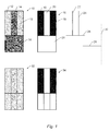
- the method may generate image 10 showing the statistic determined for each of the individual pixels as a function of the individual pixels. If the statistic is median image intensity as described above, image 10 shown in FIG. 1 may be a median image for one channel (one detection subsystem or one detector) of the inspection system, and other images may be separately generated for other channels of the inspection system.
- first segments 12 in image 10 may be defined to include pixels having values for the statistic in one range
- first segments 14 may be defined to include pixels having values for the statistic in another range different from the first. Therefore, the pixels in the image can be separated into first segments based on the statistic. Assigning the pixels to the first segments does not necessarily include generating an image as described above and using the image for the first segmentation may be performed in any other suitable manner.
- the method also includes detecting one or more edges between the first segments in an image of the first segments.
- the method includes generating the image of the first segments by labeling the individual pixels based on the first segments to which the individual pixels were assigned. For example, as shown in FIG. 1 , image 16 of the first segments may be generated by labeling the individual pixels of image 10 based on the first segments to which the individual pixels were assigned. Edge detection may then be applied to the labeled image. In this manner, MBS may be applied to median image 10 to generate image 16 showing the labeled first segments.
- image 16 may be a binary image with one of the first segments (first segments 12 ) shown as black regions 18 in the image and the other of the first segments (first segments 14 ) shown as white regions 20 in the image.
- the image showing the labeled first segments may then be used as a segmentation mask for other steps described herein (e.g., by overlaying it with an image acquired for the wafer such that pixels within the different segments can be identified based on their location within the mask).
- the image showing the first segments may also be labeled in any other suitable manner (e.g., via color differences, gray level differences, alphanumeric differences, and the like). That image may then be used to detect the edge(s) of the first segments as described further herein.
- the one or more edges include at least one edge that extends in the x direction, at least one edge that extends in the y direction, or a combination of at least one edge that extends in the x direction and at least one edge that extends in the y direction.
- edge detection may include horizontal and/or vertical edge detection.
- edge detection may add 1 to the horizontal edge at the ith location if (i, j ⁇ 1), (i, j+1) belong to different segments.
- edge detection may add 1 to the vertical edge at the jth location if (i ⁇ 1, j), (i+1, j) belong to different segments. In the example shown in FIG.
- edge detection may be performed in a number of other different ways.
- the method includes modifying the one or more detected edges before generating the edge map described further herein based on spatial characteristics of the one or more detected edges.
- This step may include “pruning” redundant edges. For example, due to physical structure roughness and inspection system resolution limitations, the edge of segments in an image is not always clean cut. Therefore, the edge detection step may detect multiple edges (redundant edges) that are substantially close together around a real physical edge. As such, the one or more detected edges may be modified using, for example, a dilation algorithm to merge (or reduce) the edges that are substantially close to one another into one edge.
- the dilation algorithm may include any suitable dilation algorithm known in the art.
- the method also includes generating an edge map by projecting the one or more edges across an area corresponding to the image for the wafer.
- the methods described herein may perform projection-based segmentation (PBS) based on edge information.
- edge map 32 may be generated as a grid from the edge projection of the horizontal and vertical edges shown in FIG. 1 (edges 22 , 24 and 28 ). Projecting the one or more edges may include extending any edges that were detected and do not extend across the entire image such that they do extend across the entire image. In other words, projecting the edge(s) may include extending an edge along its length such that it spans the entire image area.
- Detecting edges based on a statistic-based (e.g., median intensity-based) segment map and then projecting the edge(s) in the x and/or y directions can greatly help to reduce the ambiguity of the edge(s) compared to intensity-based projection. As such, this approach can be used to accurately segment frame images for the underlying structure patterns.
- the edge detection described herein that can be performed on a segment map and projection based on the edge map is also advantageously stable (with respect to any intensity variations in the light detected from the wafer that is used to form the image for the wafer). For example, an MBS segment map is stable for performing edge detection in x and y.
- projection based on the x and y edges is much more stable than edge projection based on other characteristics of the image for the wafer.
- the method also includes assigning the individual pixels to second segments by applying the first segments and the edge map to the image for the wafer thereby segmenting the image. Therefore, the embodiments described herein may segment (and label) the frame image based on the edges.
- the method may segment the pixels based on a combination of image intensity (used to define the first segments that are applied to the image) and intensity change pattern (used to define the edge map that is applied to the image) to accurately segment the underlying structures. For example, even relatively thin vertical areas with relatively low image intensity can be segmented out with the approaches described herein.
- edge projection in x and y described herein is substantially stable for reconstructing the segment map (for the second segments).
- assigning the individual pixels to the second segments includes generating the second segments based on the first segments and the edge map and applying the second segments to the individual pixels.
- the segmentation mask (or image 16 showing the first segments) may be combined with the grid (or edge map 32 showing the edges) to generate second segment groups shown in image 34 in FIG. 1 .
- this image shows the second segment groups and may be used as a second segmentation mask as described above.
- Assigning the individual pixels to the second segments may, however, be performed in any other suitable manner.
- Defect detection is performed based on the second segments to which the individual pixels are assigned.
- the embodiments described herein can be used as pre-processing method(s) to separate regions into different segments, but are not themselves an inspection or defect detection algorithm.
- the embodiments described herein can be used for pre-processing for any inspection algorithm. In this manner, defect detection may be performed in any suitable manner using any suitable method and/or algorithm.
- Steps of the method are performed by a computer system, which may be configured as described further herein.
- assigning the individual pixels to the first segments results in the individual pixels having different levels of noise assigned to different first segments.
- the methods described herein basically segment low intensity segments from high intensity segments in the form of rectangular bounding boxes. Therefore, the methods described herein essentially separate relatively low noise segments from relatively high noise segments, and the segments having different noise levels can then be processed separately during defect detection such that defects of interest (DOIs) can be detected in each of the segments regardless of the noise levels (e.g., by adjusting a threshold that is applied to the pixels), which also suppresses nuisance, noise, and background signal detection.
- DOIs defects of interest
- At least one of the first segments corresponds to a region on the wafer containing structures having a first characteristic
- at least another of the first segments corresponds to a region on the wafer containing structures having a second characteristic that is different than the first characteristic.
- the first segments since wafer structures that have different characteristics will affect the light from the wafer detected by the inspection system in different ways and since the first segments may be defined based on a statistic related to the image of the wafer (e.g., median image intensity), the first segments can be used to separate different regions of the wafer containing different structures.
- the first segments are defined based on a statistic of a characteristic of the individual pixels, instead of the characteristic itself, the first segments can be used to separate the regions with relatively high accuracy.
- At least one of the second segments corresponds to a region on the wafer containing structures having a first characteristic
- at least another of the second segments corresponds to a region on the wafer containing structures having a second characteristic that is different than the first characteristic.
- the second segments since the second segments are based, at least in part, on the first segments and since different first segments may, as described above, correspond to different regions containing structures having different characteristics, the second segments may also correspond to different regions containing structures having different characteristics.
- At least one of the first segments corresponds to a page break region of a device being fabricated on the wafer, and at least another of the first segments corresponds to an array region of the device.
- Page breaks are generally defined in the art as regions of a die separating substantially continuous regions of physical memory. Each of the continuous regions of physical memory may be commonly referred to as a page frame. Inside a dark field array region, there is no substantial feature difference and therefore no substantial intensity difference, only some background noise. However, since the page breaks include dramatically different structures than the array regions, there will be a substantial intensity difference in the image for the page breaks compared to the array regions. Therefore, the embodiments can separate an array segment from a page break segment. As described further herein, median intensity may be the statistic of the characteristic of the individual pixels that is used to assign the individual pixels to the first segments. Using median intensity as described herein is advantageous because it is stable for differentiating array from page break in terms of intensity difference.
- At least one of the second segments corresponds to a page break region of a device being fabricated on the wafer, and at least another of the second segments corresponds to an array region of the device.
- the second segments are based, at least in part, on the first segments and since some of the first segments may, as described above, correspond to page break regions while other first segments may correspond to array regions, some of the second segments may also correspond to page break regions and other second segments may correspond to array regions.
- the method is performed during scanning of the wafer by the inspection system. For example, as image frames are acquired for a wafer during scanning, the method may be performed for each or at least some of the image frames. In this manner, the method may be performed in real time during inspection by a computer subsystem of an inspection system, which may be configured as described further herein.
- the image for the wafer includes one of multiple image frames acquired sequentially for different areas on the wafer during scanning of the wafer by the inspection system.
- a detector or detection subsystem of the inspection system may capture multiple image frames as the wafer is moved relative to the inspection system or vice versa. Therefore, the image frames may be acquired at different positions on the wafer.
- the method described herein may be performed for any or all of those image frames.
- the method is performed for more than one of the multiple image frames. In this manner, the method may be performed independently and separately for each image frame on a frame-by-frame basis.
- the image for the wafer includes one of multiple image frames acquired simultaneously for one area on the wafer by multiple detection subsystems of the inspection system, and the method includes assigning individual pixels in at least one other of the multiple image frames to the second segments by applying the first segments and the edge map to the at least one other of the multiple image frames.
- the segmentation result generated using any one frame image can be applied to image frames across other detection subsystems (or “channels”) of the inspection system for the same job. In this manner, the segmentation determined for image frames generated by one channel may, in some instances, be applied to an image frame generated by another channel.
- the inspection system is a dark field inspection system. Therefore, the embodiments described herein may be used for segmentation on a dark field inspection system, which may be configured as described further herein. In addition, the embodiments described herein improve the accuracy, stability, and ease of use of the segmentation of wafer images produced by a dark field scanning inspection system. However, the embodiments described herein are not specific to a particular wafer or layer or a specific inspection system. For example, the method may be used to segment any images, no matter what kind of inspection system was used to acquire the images.
- the method may also include storing results of any of the step(s) of the method in a computer-readable storage medium.
- the results may include any of the results described herein and may be stored in any manner known in the art.
- the storage medium may include any suitable storage medium known in the art.
- FIG. 2 Another embodiment relates to a non-transitory computer-readable medium storing program instructions executable on a computer system for performing a method (i.e., a computer-implemented method) for segmenting pixels in an image of a wafer for defect detection.
- a method i.e., a computer-implemented method
- FIG. 2 One such embodiment is shown in FIG. 2 .
- computer-readable medium 36 stores program instructions 38 executable on computer system 40 for performing the method described above.
- the computer-implemented method for which the program instructions are executable may include any other step(s) of any other method(s) described herein.
- Program instructions 38 implementing methods such as those described herein may be stored on computer-readable medium 40 .
- the computer-readable medium may be a storage medium such as a magnetic or optical disk, or a magnetic tape or any other suitable non-transitory computer-readable medium known in the art.
- the program instructions may be implemented in any of various ways, including procedure-based techniques, component-based techniques, and/or object-oriented techniques, among others.
- the program instructions may be implemented using Matlab, Visual Basic, ActiveX controls, C, C++ objects, C#, JavaBeans. Microsoft Foundation Classes (“MFC”), or other technologies or methodologies, as desired.
- Computer system 40 may take various forms, including a personal computer system, mainframe computer system, workstation, system computer, image computer, programmable image computer, parallel processor, or any other device known in the art.
- computer system may be broadly defined to encompass any device having one or more processors, which executes instructions from a memory medium.
- FIG. 3 An additional embodiment relates to a system configured to segment pixels in an image of a wafer for defect detection.
- system 42 includes inspection subsystem 44 and computer subsystem 46 .
- the inspection subsystem is configured to generate an image for a wafer.
- the inspection subsystem includes light source 48 such as a laser.
- Light source 48 is configured to direct light to polarizing component 50 .
- the inspection subsystem may include more than one polarizing component (not shown), each of which may be positioned independently in the path of the light from the light source. Each of the polarizing components may be configured to alter the polarization of the light from the light source in a different manner.
- the inspection subsystem may be configured to move the polarizing components into and out of the path of the light from the light source in any suitable manner depending on which polarization setting is selected for illumination of the wafer during a scan.
- the polarization setting used for the illumination of the wafer during a scan may include p-polarized (P), s-polarized (S), or circularly polarized (C).
- Light exiting polarizing component 50 is directed to wafer 52 at an oblique angle of incidence, which may include any suitable oblique angle of incidence.
- the inspection subsystem may also include one or more optical components (not shown) that are configured to direct light from light source 48 to polarizing component 50 or from polarizing component 50 to wafer 52 .
- the optical components may include any suitable optical components known in the art such as, but not limited to, a reflective optical component.
- the light source, the polarizing component, and/or the one or more optical components may be configured to direct the light to the wafer at one or more angles of incidence (e.g., an oblique angle of incidence and/or a substantially normal angle of incidence).
- the inspection subsystem may be configured to perform the scanning by scanning the light over the wafer in any suitable manner.
- Light scattered from wafer 52 may be collected and detected by multiple channels of the inspection subsystem during scanning.
- Lens 54 may include a refractive optical element as shown in FIG. 3 .
- lens 54 may include one or more refractive optical elements and/or one or more reflective optical elements.
- Light collected by lens 54 may be directed to polarizing component 56 , which may include any suitable polarizing component known in the art.
- the inspection subsystem may include more than one polarizing component (not shown), each of which may be positioned independently in the path of the light collected by the lens. Each of the polarizing components may be configured to alter the polarization of the light collected by the lens in a different manner.
- the inspection subsystem may be configured to move the polarizing components into and out of the path of the light collected by the lens in any suitable manner depending on which polarization setting is selected for detection of the light collected by lens 54 during scanning.
- the polarization setting used for the detection of the light collected by lens 54 during scanning may include any of the polarization settings described herein (e.g., P, S, and unpolarized (N)).
- Detector 58 may include any suitable detector known in the art such as a charge coupled device (CCD) or another type of imaging detector. Detector 58 is configured to generate an image that is responsive to the scattered light collected by lens 54 and transmitted by polarizing component 56 if positioned in the path of the collected scattered light. Therefore, lens 54 , polarizing component 56 if positioned in the path of the light collected by lens 54 , and detector 58 form one channel of the inspection subsystem. This channel of the inspection subsystem may include any other suitable optical components (not shown) known in the art such as a Fourier filtering component.
- Lens 60 Light scattered from wafer 52 at different angles may be collected by lens 60 .
- Lens 60 may be configured as described above.
- Light collected by lens 60 may be directed to polarizing component 62 , which may include any suitable polarizing component known in the art.
- the inspection subsystem may include more than one polarizing component (not shown), each of which may be positioned independently in the path of the light collected by the lens.
- Each of the polarizing components may be configured to alter the polarization of the light collected by the lens in a different manner.
- the inspection subsystem may be configured to move the polarizing components into and out of the path of the light collected by the lens in any suitable manner depending on which polarization setting is selected for detection of the light collected by lens 60 during scanning.
- the polarization setting used for detection of the light collected by lens 60 during scanning may include P, S, or N.
- Light exiting polarizing component 62 is directed to detector 64 , which may be configured as described above.
- Detector 64 is also configured to generate an image that is responsive to the collected scattered light that passes through polarizing component 62 if positioned in the path of the scattered light. Therefore, lens 60 , polarizing component 62 if positioned in the path of the light collected by lens 60 , and detector 64 may form another channel of the inspection subsystem. This channel may also include any other optical components (not shown) described above.
- lens 60 may be configured to collect light scattered from the wafer at polar angles from about 20 degrees to about 70 degrees.
- lens 60 may be configured as a reflective optical component (not shown) that is configured to collect light scattered from the wafer at azimuthal angles of about 360 degrees.
- the inspection subsystem shown in FIG. 3 may also include one or more other channels (not shown).
- the inspection subsystem may include an additional channel, which may include any of the optical components described herein such as a lens, one or more polarizing components, and a detector, configured as a side channel.
- the lens, the one or more polarizing components, and the detector may be further configured as described herein.
- the side channel may be configured to collect and detect light that is scattered out of the plane of incidence (e.g., the side channel may include a lens, which is centered in a plane that is substantially perpendicular to the plane of incidence, and a detector configured to detect light collected by the lens).
- Computer subsystem 46 is configured to acquire the image(s) generated by the inspection subsystem.
- image(s) generated by the detectors during scanning may be provided to computer subsystem 46 .
- the computer subsystem may be coupled to each of the detectors (e.g., by one or more transmission media shown by the dashed lines in FIG. 3 , which may include any suitable transmission media known in the art) such that the computer subsystem may receive the image(s) generated by the detectors.
- the computer subsystem may be coupled to each of the detectors in any suitable manner.
- the image(s) generated by the detectors during scanning of the wafer may include any of the image(s) described herein.
- the computer subsystem is configured for performing the steps of the method described herein.
- the computer subsystem may also be configured to perform any other step(s) of any method embodiment(s) described herein.
- the computer subsystem, the inspection subsystem, and the system may be further configured as described herein.
- FIG. 3 is provided herein to generally illustrate one configuration of an inspection subsystem that may be included in the system embodiments described herein.
- the inspection subsystem configuration described herein may be altered to optimize the performance of the inspection subsystem as is normally performed when designing a commercial inspection system.
- the systems described herein may be implemented using an existing inspection system (e.g., by adding functionality described herein to an existing inspection system) such as the Puma 90xx, 91xx, and 93xx series of tools that are commercially available from KLA-Tencor, Milpitas, Calif.
- the methods described herein may be provided as optional functionality of the system (e.g., in addition to other functionality of the system).
- the system described herein may be designed “from scratch” to provide a completely new system.
Abstract
Description
Claims (20)
Priority Applications (6)
| Application Number | Priority Date | Filing Date | Title |
|---|---|---|---|
| US13/742,259 US8831334B2 (en) | 2012-01-20 | 2013-01-15 | Segmentation for wafer inspection |
| PCT/US2013/021940 WO2013109755A1 (en) | 2012-01-20 | 2013-01-17 | Segmentation for wafer inspection |
| JP2014553408A JP2015511310A (en) | 2012-01-20 | 2013-01-17 | Segmentation for wafer inspection |
| KR1020147023290A KR102009494B1 (en) | 2012-01-20 | 2013-01-17 | Segmentation for wafer inspection |
| DE112013000627.8T DE112013000627T5 (en) | 2012-01-20 | 2013-01-17 | Segmentation for wafer inspection |
| TW102102111A TWI562098B (en) | 2012-01-20 | 2013-01-18 | Computer-implemented method,non-transitory computer-readable medium, and system for segmentation for wafer inspection |
Applications Claiming Priority (2)
| Application Number | Priority Date | Filing Date | Title |
|---|---|---|---|
| US201261588871P | 2012-01-20 | 2012-01-20 | |
| US13/742,259 US8831334B2 (en) | 2012-01-20 | 2013-01-15 | Segmentation for wafer inspection |
Publications (2)
| Publication Number | Publication Date |
|---|---|
| US20130188859A1 US20130188859A1 (en) | 2013-07-25 |
| US8831334B2 true US8831334B2 (en) | 2014-09-09 |
Family
ID=48797246
Family Applications (1)
| Application Number | Title | Priority Date | Filing Date |
|---|---|---|---|
| US13/742,259 Active 2033-02-13 US8831334B2 (en) | 2012-01-20 | 2013-01-15 | Segmentation for wafer inspection |
Country Status (6)
| Country | Link |
|---|---|
| US (1) | US8831334B2 (en) |
| JP (1) | JP2015511310A (en) |
| KR (1) | KR102009494B1 (en) |
| DE (1) | DE112013000627T5 (en) |
| TW (1) | TWI562098B (en) |
| WO (1) | WO2013109755A1 (en) |
Cited By (5)
| Publication number | Priority date | Publication date | Assignee | Title |
|---|---|---|---|---|
| US9506873B2 (en) | 2014-04-15 | 2016-11-29 | Kla-Tencor Corp. | Pattern suppression in logic for wafer inspection |
| US9816939B2 (en) | 2014-07-22 | 2017-11-14 | Kla-Tencor Corp. | Virtual inspection systems with multiple modes |
| US20180045937A1 (en) * | 2016-08-10 | 2018-02-15 | Zeta Instruments, Inc. | Automated 3-d measurement |
| US10489902B2 (en) | 2015-10-21 | 2019-11-26 | Samsung Electronics Co., Ltd. | Inspection apparatus, semiconductor device manufacturing system including the same, and method of manufacturing a semiconductor device using the same |
| US20220301133A1 (en) * | 2021-03-16 | 2022-09-22 | Kla Corporation | Segmentation of design care areas with a rendered design image |
Families Citing this family (15)
| Publication number | Priority date | Publication date | Assignee | Title |
|---|---|---|---|---|
| TWI493177B (en) * | 2013-10-15 | 2015-07-21 | Benq Materials Corp | Method of detecting defect on optical film with periodic structure and device thereof |
| US9262821B2 (en) * | 2014-05-12 | 2016-02-16 | Kla-Tencor Corp. | Inspection recipe setup from reference image variation |
| US9569834B2 (en) | 2015-06-22 | 2017-02-14 | Kla-Tencor Corporation | Automated image-based process monitoring and control |
| JP6779229B2 (en) * | 2015-04-30 | 2020-11-04 | ケーエルエー コーポレイション | Process monitoring and control based on automated images |
| US10186028B2 (en) * | 2015-12-09 | 2019-01-22 | Kla-Tencor Corporation | Defect signal to noise enhancement by reducing die to die process noise |
| US10365639B2 (en) * | 2016-01-06 | 2019-07-30 | Kla-Tencor Corporation | Feature selection and automated process window monitoring through outlier detection |
| JP2017134596A (en) * | 2016-01-27 | 2017-08-03 | 株式会社東芝 | Image processing method and process simulation device |
| US11295432B2 (en) * | 2017-06-29 | 2022-04-05 | Kla-Tencor Corporation | Broad band plasma inspection based on a nuisance map |
| EP3867942A1 (en) * | 2018-10-19 | 2021-08-25 | ASML Netherlands B.V. | System and method for aligning electron beams in multi-beam inspection apparatus |
| WO2020133046A1 (en) * | 2018-12-27 | 2020-07-02 | 深圳配天智能技术研究院有限公司 | Defect detection method and device |
| US11676260B2 (en) * | 2019-09-26 | 2023-06-13 | Kla Corporation | Variation-based segmentation for wafer defect detection |
| US11610296B2 (en) | 2020-01-09 | 2023-03-21 | Kla Corporation | Projection and distance segmentation algorithm for wafer defect detection |
| KR20220001125A (en) * | 2020-06-29 | 2022-01-05 | 삼성전자주식회사 | Method and apparatus for detecting defects on substrate |
| TW202316535A (en) * | 2021-04-05 | 2023-04-16 | 美商科磊股份有限公司 | Semantic image segmentation for semiconductor-based applications |
| CN115063413B (en) * | 2022-08-04 | 2022-11-11 | 宁波鑫芯微电子科技有限公司 | Feature extraction method for abnormal data of super-large-scale wafer |
Citations (376)
| Publication number | Priority date | Publication date | Assignee | Title |
|---|---|---|---|---|
| US3495269A (en) | 1966-12-19 | 1970-02-10 | Xerox Corp | Electrographic recording method and apparatus with inert gaseous discharge ionization and acceleration gaps |
| US3496352A (en) | 1967-06-05 | 1970-02-17 | Xerox Corp | Self-cleaning corona generating apparatus |
| US3909602A (en) | 1973-09-27 | 1975-09-30 | California Inst Of Techn | Automatic visual inspection system for microelectronics |
| US4015203A (en) | 1975-12-31 | 1977-03-29 | International Business Machines Corporation | Contactless LSI junction leakage testing method |
| US4247203A (en) | 1978-04-03 | 1981-01-27 | Kla Instrument Corporation | Automatic photomask inspection system and apparatus |
| US4347001A (en) | 1978-04-03 | 1982-08-31 | Kla Instruments Corporation | Automatic photomask inspection system and apparatus |
| US4378159A (en) | 1981-03-30 | 1983-03-29 | Tencor Instruments | Scanning contaminant and defect detector |
| EP0032197B1 (en) | 1980-01-09 | 1984-04-11 | International Business Machines Corporation | Test procedures for integrated semi-conductor circuits allowing the electric determination of certain tolerances during the photolithographic stages |
| US4448532A (en) | 1981-03-31 | 1984-05-15 | Kla Instruments Corporation | Automatic photomask inspection method and system |
| US4475122A (en) | 1981-11-09 | 1984-10-02 | Tre Semiconductor Equipment Corporation | Automatic wafer alignment technique |
| US4532650A (en) | 1983-05-12 | 1985-07-30 | Kla Instruments Corporation | Photomask inspection apparatus and method using corner comparator defect detection algorithm |
| US4555798A (en) | 1983-06-20 | 1985-11-26 | Kla Instruments Corporation | Automatic system and method for inspecting hole quality |
| US4578810A (en) | 1983-08-08 | 1986-03-25 | Itek Corporation | System for printed circuit board defect detection |
| US4579455A (en) | 1983-05-09 | 1986-04-01 | Kla Instruments Corporation | Photomask inspection apparatus and method with improved defect detection |
| US4595289A (en) | 1984-01-25 | 1986-06-17 | At&T Bell Laboratories | Inspection system utilizing dark-field illumination |
| US4599558A (en) | 1983-12-14 | 1986-07-08 | Ibm | Photovoltaic imaging for large area semiconductors |
| US4633504A (en) | 1984-06-28 | 1986-12-30 | Kla Instruments Corporation | Automatic photomask inspection system having image enhancement means |
| US4641353A (en) | 1983-09-16 | 1987-02-03 | Fujitsu Limited | Inspection method and apparatus for a mask pattern used in semiconductor device fabrication |
| US4641967A (en) | 1985-10-11 | 1987-02-10 | Tencor Instruments | Particle position correlator and correlation method for a surface scanner |
| US4734721A (en) | 1985-10-04 | 1988-03-29 | Markem Corporation | Electrostatic printer utilizing dehumidified air |
| US4748327A (en) | 1985-06-13 | 1988-05-31 | Kabushiki Kaisha Toshiba | Method of inspecting masks and apparatus thereof |
| US4758094A (en) | 1987-05-15 | 1988-07-19 | Kla Instruments Corp. | Process and apparatus for in-situ qualification of master patterns used in patterning systems |
| US4766324A (en) | 1987-08-07 | 1988-08-23 | Tencor Instruments | Particle detection method including comparison between sequential scans |
| US4799175A (en) | 1984-06-12 | 1989-01-17 | Dainippon Screen Mfg., Co. | System for inspecting pattern defects of printed wiring boards |
| US4805123A (en) | 1986-07-14 | 1989-02-14 | Kla Instruments Corporation | Automatic photomask and reticle inspection method and apparatus including improved defect detector and alignment sub-systems |
| US4812756A (en) | 1987-08-26 | 1989-03-14 | International Business Machines Corporation | Contactless technique for semicondutor wafer testing |
| US4814829A (en) | 1986-06-12 | 1989-03-21 | Canon Kabushiki Kaisha | Projection exposure apparatus |
| US4817123A (en) | 1984-09-21 | 1989-03-28 | Picker International | Digital radiography detector resolution improvement |
| US4845558A (en) | 1987-12-03 | 1989-07-04 | Kla Instruments Corporation | Method and apparatus for detecting defects in repeated microminiature patterns |
| US4877326A (en) | 1988-02-19 | 1989-10-31 | Kla Instruments Corporation | Method and apparatus for optical inspection of substrates |
| US4926489A (en) | 1983-03-11 | 1990-05-15 | Kla Instruments Corporation | Reticle inspection system |
| US4928313A (en) | 1985-10-25 | 1990-05-22 | Synthetic Vision Systems, Inc. | Method and system for automatically visually inspecting an article |
| US5046109A (en) | 1986-03-12 | 1991-09-03 | Nikon Corporation | Pattern inspection apparatus |
| US5124927A (en) | 1990-03-02 | 1992-06-23 | International Business Machines Corp. | Latent-image control of lithography tools |
| US5189481A (en) | 1991-07-26 | 1993-02-23 | Tencor Instruments | Particle detector for rough surfaces |
| US5355212A (en) | 1993-07-19 | 1994-10-11 | Tencor Instruments | Process for inspecting patterned wafers |
| US5444480A (en) | 1992-10-26 | 1995-08-22 | Kirin Techno-System Corporation | Method of inspecting solid body for foreign matter |
| US5453844A (en) | 1993-07-21 | 1995-09-26 | The University Of Rochester | Image data coding and compression system utilizing controlled blurring |
| US5481624A (en) | 1992-04-27 | 1996-01-02 | Mitsubishi Denki Kabushiki Kaisha | Mask inspecting method and mask detector |
| US5485091A (en) | 1995-05-12 | 1996-01-16 | International Business Machines Corporation | Contactless electrical thin oxide measurements |
| US5497381A (en) | 1993-10-15 | 1996-03-05 | Analog Devices, Inc. | Bitstream defect analysis method for integrated circuits |
| US5528153A (en) | 1994-11-07 | 1996-06-18 | Texas Instruments Incorporated | Method for non-destructive, non-contact measurement of dielectric constant of thin films |
| US5544256A (en) | 1993-10-22 | 1996-08-06 | International Business Machines Corporation | Automated defect classification system |
| US5563702A (en) | 1991-08-22 | 1996-10-08 | Kla Instruments Corporation | Automated photomask inspection apparatus and method |
| US5572598A (en) | 1991-08-22 | 1996-11-05 | Kla Instruments Corporation | Automated photomask inspection apparatus |
| US5578821A (en) | 1992-05-27 | 1996-11-26 | Kla Instruments Corporation | Electron beam inspection system and method |
| US5594247A (en) | 1995-07-07 | 1997-01-14 | Keithley Instruments, Inc. | Apparatus and method for depositing charge on a semiconductor wafer |
| US5608538A (en) | 1994-08-24 | 1997-03-04 | International Business Machines Corporation | Scan line queuing for high performance image correction |
| US5619548A (en) | 1995-08-11 | 1997-04-08 | Oryx Instruments And Materials Corp. | X-ray thickness gauge |
| US5621519A (en) | 1995-07-31 | 1997-04-15 | Neopath, Inc. | Imaging system transfer function control method and apparatus |
| US5644223A (en) | 1995-05-12 | 1997-07-01 | International Business Machines Corporation | Uniform density charge deposit source |
| US5650731A (en) | 1995-05-12 | 1997-07-22 | International Business Machines Corporation | Photovoltaic oxide charge measurement probe technique |
| US5661408A (en) | 1995-03-01 | 1997-08-26 | Qc Solutions, Inc. | Real-time in-line testing of semiconductor wafers |
| US5689614A (en) | 1990-01-19 | 1997-11-18 | Applied Materials, Inc. | Rapid thermal heating apparatus and control therefor |
| US5694478A (en) | 1994-12-15 | 1997-12-02 | Minnesota Mining And Manufacturing Company | Method and apparatus for detecting and identifying microbial colonies |
| US5696835A (en) | 1994-01-21 | 1997-12-09 | Texas Instruments Incorporated | Apparatus and method for aligning and measuring misregistration |
| US5703969A (en) | 1994-01-21 | 1997-12-30 | Texas Instruments Incorporated | System and method for recognizing visual indicia |
| US5742658A (en) | 1996-05-23 | 1998-04-21 | Advanced Micro Devices, Inc. | Apparatus and method for determining the elemental compositions and relative locations of particles on the surface of a semiconductor wafer |
| US5754678A (en) | 1996-01-17 | 1998-05-19 | Photon Dynamics, Inc. | Substrate inspection apparatus and method |
| US5767691A (en) | 1993-12-22 | 1998-06-16 | International Business Machines Corporation | Probe-oxide-semiconductor method and apparatus for measuring oxide charge on a semiconductor wafer |
| US5767693A (en) | 1996-09-04 | 1998-06-16 | Smithley Instruments, Inc. | Method and apparatus for measurement of mobile charges with a corona screen gun |
| US5771317A (en) | 1994-08-24 | 1998-06-23 | International Business Machines Corporation | Image resize using sinc filter in linear lumen space |
| US5773989A (en) | 1995-07-14 | 1998-06-30 | University Of South Florida | Measurement of the mobile ion concentration in the oxide layer of a semiconductor wafer |
| US5774179A (en) | 1994-12-28 | 1998-06-30 | Minister Of National Defence | Method and system for fast microscanning |
| EP0370322B1 (en) | 1988-11-23 | 1998-07-08 | Schlumberger Technologies, Inc. | Method and apparatus for alignment of images |
| US5795685A (en) | 1997-01-14 | 1998-08-18 | International Business Machines Corporation | Simple repair method for phase shifting masks |
| US5822218A (en) | 1996-08-27 | 1998-10-13 | Clemson University | Systems, methods and computer program products for prediction of defect-related failures in integrated circuits |
| US5831865A (en) | 1995-06-20 | 1998-11-03 | Advanced Micro Devices, Inc. | Method and system for declusturing semiconductor defect data |
| US5834941A (en) | 1997-08-11 | 1998-11-10 | Keithley Instruments, Inc. | Mobile charge measurement using corona charge and ultraviolet light |
| US5852232A (en) | 1997-01-02 | 1998-12-22 | Kla-Tencor Corporation | Acoustic sensor as proximity detector |
| US5866806A (en) | 1996-10-11 | 1999-02-02 | Kla-Tencor Corporation | System for locating a feature of a surface |
| US5874733A (en) | 1997-10-16 | 1999-02-23 | Raytheon Company | Convergent beam scanner linearizing method and apparatus |
| US5884242A (en) | 1996-04-11 | 1999-03-16 | Micron Technology, Inc. | Focus spot detection method and system |
| US5889593A (en) | 1997-02-26 | 1999-03-30 | Kla Instruments Corporation | Optical system and method for angle-dependent reflection or transmission measurement |
| US5917332A (en) | 1996-05-09 | 1999-06-29 | Advanced Micro Devices, Inc. | Arrangement for improving defect scanner sensitivity and scanning defects on die of a semiconductor wafer |
| US5932377A (en) | 1998-02-24 | 1999-08-03 | International Business Machines Corporation | Exact transmission balanced alternating phase-shifting mask for photolithography |
| US5940458A (en) | 1997-05-10 | 1999-08-17 | Hyundai Electronics Industries Co., Ltd. | Method and compensating for time error of time/frequency generator using global positioning system |
| US5948972A (en) | 1994-12-22 | 1999-09-07 | Kla-Tencor Corporation | Dual stage instrument for scanning a specimen |
| US5955661A (en) | 1997-01-06 | 1999-09-21 | Kla-Tencor Corporation | Optical profilometer combined with stylus probe measurement device |
| US5965306A (en) | 1997-10-15 | 1999-10-12 | International Business Machines Corporation | Method of determining the printability of photomask defects |
| US5978501A (en) | 1997-01-03 | 1999-11-02 | International Business Machines Corporation | Adaptive inspection method and system |
| US5980187A (en) | 1997-04-16 | 1999-11-09 | Kla-Tencor Corporation | Mechanism for transporting semiconductor-process masks |
| US5986263A (en) | 1996-03-29 | 1999-11-16 | Hitachi, Ltd. | Electron beam inspection method and apparatus and semiconductor manufacturing method and its manufacturing line utilizing the same |
| US5991699A (en) | 1995-05-04 | 1999-11-23 | Kla Instruments Corporation | Detecting groups of defects in semiconductor feature space |
| US5999003A (en) | 1997-12-12 | 1999-12-07 | Advanced Micro Devices, Inc. | Intelligent usage of first pass defect data for improved statistical accuracy of wafer level classification |
| US6011404A (en) | 1997-07-03 | 2000-01-04 | Lucent Technologies Inc. | System and method for determining near--surface lifetimes and the tunneling field of a dielectric in a semiconductor |
| US6014461A (en) | 1994-11-30 | 2000-01-11 | Texas Instruments Incorporated | Apparatus and method for automatic knowlege-based object identification |
| US6040912A (en) | 1998-09-30 | 2000-03-21 | Advanced Micro Devices, Inc. | Method and apparatus for detecting process sensitivity to integrated circuit layout using wafer to wafer defect inspection device |
| US6060709A (en) | 1997-12-31 | 2000-05-09 | Verkuil; Roger L. | Apparatus and method for depositing uniform charge on a thin oxide semiconductor wafer |
| US6072320A (en) | 1997-07-30 | 2000-06-06 | Verkuil; Roger L. | Product wafer junction leakage measurement using light and eddy current |
| US6076465A (en) | 1996-09-20 | 2000-06-20 | Kla-Tencor Corporation | System and method for determining reticle defect printability |
| US6078738A (en) | 1997-05-08 | 2000-06-20 | Lsi Logic Corporation | Comparing aerial image to SEM of photoresist or substrate pattern for masking process characterization |
| US6091257A (en) | 1998-02-26 | 2000-07-18 | Verkuil; Roger L. | Vacuum activated backside contact |
| US6091846A (en) | 1996-05-31 | 2000-07-18 | Texas Instruments Incorporated | Method and system for anomaly detection |
| US6097196A (en) | 1997-04-23 | 2000-08-01 | Verkuil; Roger L. | Non-contact tunnelling field measurement for a semiconductor oxide layer |
| US6097887A (en) | 1997-10-27 | 2000-08-01 | Kla-Tencor Corporation | Software system and method for graphically building customized recipe flowcharts |
| US6104835A (en) | 1997-11-14 | 2000-08-15 | Kla-Tencor Corporation | Automatic knowledge database generation for classifying objects and systems therefor |
| US6104206A (en) | 1997-08-05 | 2000-08-15 | Verkuil; Roger L. | Product wafer junction leakage measurement using corona and a kelvin probe |
| US6117598A (en) | 1997-11-25 | 2000-09-12 | Nikon Corporation | Scanning exposure method with alignment during synchronous movement |
| US6122046A (en) | 1998-10-02 | 2000-09-19 | Applied Materials, Inc. | Dual resolution combined laser spot scanning and area imaging inspection |
| US6122017A (en) | 1998-01-22 | 2000-09-19 | Hewlett-Packard Company | Method for providing motion-compensated multi-field enhancement of still images from video |
| US6121783A (en) | 1997-04-22 | 2000-09-19 | Horner; Gregory S. | Method and apparatus for establishing electrical contact between a wafer and a chuck |
| US6137570A (en) | 1998-06-30 | 2000-10-24 | Kla-Tencor Corporation | System and method for analyzing topological features on a surface |
| US6141038A (en) | 1995-10-02 | 2000-10-31 | Kla Instruments Corporation | Alignment correction prior to image sampling in inspection systems |
| US6146627A (en) | 1992-03-09 | 2000-11-14 | Sidney Kimmel Cancer Center | Method for reducing T cell-mediated cytotoxicity in HIV using anti-idiotypic antibody |
| US6171737B1 (en) | 1998-02-03 | 2001-01-09 | Advanced Micro Devices, Inc. | Low cost application of oxide test wafer for defect monitor in photolithography process |
| US6175645B1 (en) | 1998-01-22 | 2001-01-16 | Applied Materials, Inc. | Optical inspection method and apparatus |
| EP1069609A2 (en) | 1999-07-16 | 2001-01-17 | Applied Materials, Inc. | Method for automatically identifying and classifying defects, in particular on a semiconductor wafer |
| US6184976B1 (en) | 1996-10-10 | 2001-02-06 | Samsung Electronics Co., Ltd. | Apparatus and method for measuring an aerial image using transmitted light and reflected light |
| US6184929B1 (en) | 1990-12-11 | 2001-02-06 | Fuji Xerox Co., Ltd. | Solid state imaging device and image read apparatus with polygonal photosensitive pixels |
| US6191605B1 (en) | 1997-08-18 | 2001-02-20 | Tom G. Miller | Contactless method for measuring total charge of an insulating layer on a substrate using corona charge |
| US6201999B1 (en) | 1997-06-09 | 2001-03-13 | Applied Materials, Inc. | Method and apparatus for automatically generating schedules for wafer processing within a multichamber semiconductor wafer processing tool |
| US6205239B1 (en) | 1996-05-31 | 2001-03-20 | Texas Instruments Incorporated | System and method for circuit repair |
| US6215551B1 (en) | 1994-12-08 | 2001-04-10 | Kla-Tencor Corporation | Scanning system for inspecting anomalies on surfaces |
| US6224638B1 (en) | 1996-10-21 | 2001-05-01 | Applied Materials, Inc. | Method and apparatus for scheduling wafer processing within a multiple chamber semiconductor wafer processing tool having a multiple blade robot |
| US6233719B1 (en) | 1997-10-27 | 2001-05-15 | Kla-Tencor Corporation | System and method for analyzing semiconductor production data |
| EP1065567A3 (en) | 1999-06-29 | 2001-05-16 | Applied Materials, Inc. | Integrated critical dimension control |
| US6246787B1 (en) | 1996-05-31 | 2001-06-12 | Texas Instruments Incorporated | System and method for knowledgebase generation and management |
| US6248485B1 (en) | 1999-07-19 | 2001-06-19 | Lucent Technologies Inc. | Method for controlling a process for patterning a feature in a photoresist |
| US6248486B1 (en) | 1998-11-23 | 2001-06-19 | U.S. Philips Corporation | Method of detecting aberrations of an optical imaging system |
| US6259960B1 (en) | 1996-11-01 | 2001-07-10 | Joel Ltd. | Part-inspecting system |
| US6266437B1 (en) | 1998-09-04 | 2001-07-24 | Sandia Corporation | Sequential detection of web defects |
| US6268093B1 (en) | 1999-10-13 | 2001-07-31 | Applied Materials, Inc. | Method for reticle inspection using aerial imaging |
| US6272236B1 (en) | 1998-02-24 | 2001-08-07 | Micron Technology, Inc. | Inspection technique of photomask |
| US6282309B1 (en) | 1998-05-29 | 2001-08-28 | Kla-Tencor Corporation | Enhanced sensitivity automated photomask inspection system |
| US20010017694A1 (en) | 2000-02-15 | 2001-08-30 | Nikon Corporation | Defect inspection apparatus |
| US6292582B1 (en) | 1996-05-31 | 2001-09-18 | Lin Youling | Method and system for identifying defects in a semiconductor |
| US20010022858A1 (en) | 1992-04-09 | 2001-09-20 | Olympus Optical Co., Ltd., | Image displaying apparatus |
| US20010043735A1 (en) | 1998-10-15 | 2001-11-22 | Eugene Smargiassi | Detection of wafer fragments in a wafer processing apparatus |
| US6324298B1 (en) | 1998-07-15 | 2001-11-27 | August Technology Corp. | Automated wafer defect inspection system and a process of performing such inspection |
| US20020010560A1 (en) | 1999-12-13 | 2002-01-24 | Hari Balachandran | System for mapping logical functional test data of logical integrated circuits to physical representation using pruned diagnostic list |
| US6344640B1 (en) | 1993-03-01 | 2002-02-05 | Geoffrey B. Rhoads | Method for wide field distortion-compensated imaging |
| US20020019729A1 (en) | 1997-09-17 | 2002-02-14 | Numerical Technologies, Inc. | Visual inspection and verification system |
| US20020026626A1 (en) | 2000-08-24 | 2002-02-28 | Randall John N. | Optical proximity correction |
| CN1339140A (en) | 1999-11-29 | 2002-03-06 | 奥林巴斯光学工业株式会社 | Defect inspecting system |
| JP2002071575A (en) | 2000-09-04 | 2002-03-08 | Matsushita Electric Ind Co Ltd | Defect inspecting and analyzing method and system therefor |
| US20020035461A1 (en) | 1997-09-17 | 2002-03-21 | Numerical Technologies, Inc. | Visual analysis and verification system using advanced tools |
| US20020033449A1 (en) | 2000-06-27 | 2002-03-21 | Mamoru Nakasuji | Inspection system by charged particle beam and method of manufacturing devices using the system |
| US20020035641A1 (en) | 1999-07-02 | 2002-03-21 | Yoshitoshi Kurose | Service allocating device |
| US20020035717A1 (en) | 2000-07-14 | 2002-03-21 | Ryoichi Matsuoka | Navigation method and device for pattern observation of semiconductor device |
| US6373975B1 (en) | 1999-01-25 | 2002-04-16 | International Business Machines Corporation | Error checking of simulated printed images with process window effects included |
| US6388747B2 (en) | 1998-11-30 | 2002-05-14 | Hitachi, Ltd. | Inspection method, apparatus and system for circuit pattern |
| US6393602B1 (en) | 1998-10-21 | 2002-05-21 | Texas Instruments Incorporated | Method of a comprehensive sequential analysis of the yield losses of semiconductor wafers |
| US6407373B1 (en) | 1999-06-15 | 2002-06-18 | Applied Materials, Inc. | Apparatus and method for reviewing defects on an object |
| US6415421B2 (en) | 2000-06-13 | 2002-07-02 | Mentor Graphics Corporation | Integrated verification and manufacturability tool |
| US20020088951A1 (en) | 2000-12-06 | 2002-07-11 | Chen J. Fung | Method and apparatus for detecting aberrations in an optical system |
| US20020090746A1 (en) | 2000-05-10 | 2002-07-11 | Zhiwei Xu | Method and system for detecting metal contamination on a semiconductor wafer |
| US6445199B1 (en) | 1999-12-14 | 2002-09-03 | Kla-Tencor Corporation | Methods and apparatus for generating spatially resolved voltage contrast maps of semiconductor test structures |
| US6451690B1 (en) | 2000-03-13 | 2002-09-17 | Matsushita Electronics Corporation | Method of forming electrode structure and method of fabricating semiconductor device |
| US20020134936A1 (en) | 2001-03-23 | 2002-09-26 | Miyako Matsui | Wafer inspection system and wafer inspection process using charged particle beam |
| US6459520B1 (en) | 1998-07-13 | 2002-10-01 | Canon Kabushiki Kaisha | Optical scanning apparatus and image forming apparatus using it |
| US20020144230A1 (en) | 1999-09-22 | 2002-10-03 | Dupont Photomasks, Inc. | System and method for correcting design rule violations in a mask layout file |
| US20020145734A1 (en) | 2001-02-09 | 2002-10-10 | Cory Watkins | Confocal 3D inspection system and process |
| US6466314B1 (en) | 1998-09-17 | 2002-10-15 | Applied Materials, Inc. | Reticle design inspection system |
| US6466315B1 (en) | 1999-09-03 | 2002-10-15 | Applied Materials, Inc. | Method and system for reticle inspection by photolithography simulation |
| US6470489B1 (en) | 1997-09-17 | 2002-10-22 | Numerical Technologies, Inc. | Design rule checking system and method |
| US20020164065A1 (en) | 2001-03-20 | 2002-11-07 | Numerical Technologies | System and method of providing mask defect printability analysis |
| US20020176096A1 (en) | 2001-05-22 | 2002-11-28 | Canon Kabushiki Kaisha | Position detecting method and apparatus, exposure apparatus and device manufacturing method |
| US20020181756A1 (en) | 2001-04-10 | 2002-12-05 | Hisae Shibuya | Method for analyzing defect data and inspection apparatus and review system |
| US20020186878A1 (en) | 2001-06-07 | 2002-12-12 | Hoon Tan Seow | System and method for multiple image analysis |
| JP2002365235A (en) | 2001-06-08 | 2002-12-18 | Sumitomo Mitsubishi Silicon Corp | Defect inspection method and apparatus |
| US20020192578A1 (en) | 2001-04-26 | 2002-12-19 | Kabushiki Kaisha Toshiba | Inspection method of photo mask for use in manufacturing semiconductor device |
| US20030004699A1 (en) | 2001-06-04 | 2003-01-02 | Choi Charles Y. | Method and apparatus for evaluating an integrated circuit model |
| US20030014146A1 (en) | 2001-07-12 | 2003-01-16 | Kabushiki Kaisha Toshiba | Dangerous process/pattern detection system and method, danger detection program, and semiconductor device manufacturing method |
| US20030017664A1 (en) | 2001-03-30 | 2003-01-23 | Applied Materials, Inc | Kill index analysis for automatic defect classification in semiconductor wafers |
| US6513151B1 (en) | 2000-09-14 | 2003-01-28 | Advanced Micro Devices, Inc. | Full flow focus exposure matrix analysis and electrical testing for new product mask evaluation |
| US20030022401A1 (en) | 2001-07-24 | 2003-01-30 | Hitachi, Ltd. | Semiconductor device inspection method |
| US20030033046A1 (en) | 2001-07-17 | 2003-02-13 | Hitachi, Ltd. | Method and system for manufacturing semiconductor devices |
| CN1398348A (en) | 2000-10-02 | 2003-02-19 | 应用材料有限公司 | Defect source identifier |
| US6526164B1 (en) | 1999-05-27 | 2003-02-25 | International Business Machines Corporation | Intelligent photomask disposition |
| US6529621B1 (en) | 1998-12-17 | 2003-03-04 | Kla-Tencor | Mechanisms for making and inspecting reticles |
| US20030048939A1 (en) | 1999-05-18 | 2003-03-13 | Applied Materials, Inc. | Method of and apparatus for inspection of articles by comparison with a master |
| US20030048458A1 (en) | 2001-06-26 | 2003-03-13 | Walter Mieher | Method for determining lithographic focus and exposure |
| US6539106B1 (en) | 1999-01-08 | 2003-03-25 | Applied Materials, Inc. | Feature-based defect detection |
| US20030057971A1 (en) | 2001-09-27 | 2003-03-27 | Hidetoshi Nishiyama | Inspection method using a charged particle beam and inspection device based thereon |
| US20030076989A1 (en) * | 2001-10-24 | 2003-04-24 | Maayah Kais Jameel | Automated repetitive array microstructure defect inspection |
| US20030094572A1 (en) | 2001-11-19 | 2003-05-22 | Hitachi, Ltd. | Inspection system and inspection process for wafer with circuit using charged-particle beam |
| US6569691B1 (en) | 2000-03-29 | 2003-05-27 | Semiconductor Diagnostics, Inc. | Measurement of different mobile ion concentrations in the oxide layer of a semiconductor wafer |
| US20030098805A1 (en) | 1999-11-29 | 2003-05-29 | Bizjak Karl M. | Input level adjust system and method |
| US6581193B1 (en) | 2001-06-13 | 2003-06-17 | Kla-Tencor | Apparatus and methods for modeling process effects and imaging effects in scanning electron microscopy |
| US20030128870A1 (en) | 2002-01-08 | 2003-07-10 | Pease R. Fabian W. | System and method for aerial image sensing |
| US6593748B1 (en) | 2001-07-12 | 2003-07-15 | Advanced Micro Devices, Inc. | Process integration of electrical thickness measurement of gate oxide and tunnel oxides by corona discharge technique |
| US6597193B2 (en) | 2001-01-26 | 2003-07-22 | Semiconductor Diagnostics, Inc. | Steady state method for measuring the thickness and the capacitance of ultra thin dielectric in the presence of substantial leakage current |
| US20030138978A1 (en) | 2001-09-20 | 2003-07-24 | Hitachi, Ltd. | Method for manufacturing semiconductor devices and method and its apparatus for processing detected defect data |
| JP2003215060A (en) | 2002-01-22 | 2003-07-30 | Tokyo Seimitsu Co Ltd | Pattern inspection method and inspection apparatus |
| US6602728B1 (en) | 2001-01-05 | 2003-08-05 | International Business Machines Corporation | Method for generating a proximity model based on proximity rules |
| US6608681B2 (en) | 1992-12-25 | 2003-08-19 | Nikon Corporation | Exposure method and apparatus |
| US6614520B1 (en) | 1997-12-18 | 2003-09-02 | Kla-Tencor Corporation | Method for inspecting a reticle |
| US20030169916A1 (en) | 2002-02-19 | 2003-09-11 | Toshiba Ceramics Co., Ltd. | Wafer inspection apparatus |
| EP1066925A3 (en) | 1999-07-09 | 2003-09-17 | Applied Materials, Inc. | Closed loop control of wafer polishing in a chemical mechanical polishing system |
| US20030173516A1 (en) | 2001-04-27 | 2003-09-18 | Atsushi Takane | Semiconductor inspection system |
| US6631511B2 (en) | 2000-09-07 | 2003-10-07 | Infineon Technologies Ag | Generating mask layout data for simulation of lithographic processes |
| US20030192015A1 (en) | 2002-04-04 | 2003-10-09 | Numerical Technologies, Inc. | Method and apparatus to facilitate test pattern design for model calibration and proximity correction |
| US6636301B1 (en) | 2000-08-10 | 2003-10-21 | Kla-Tencor Corporation | Multiple beam inspection apparatus and method |
| US6642066B1 (en) | 2002-05-15 | 2003-11-04 | Advanced Micro Devices, Inc. | Integrated process for depositing layer of high-K dielectric with in-situ control of K value and thickness of high-K dielectric layer |
| US20030207475A1 (en) | 2000-11-02 | 2003-11-06 | Ebara Corporation | Electron beam apparatus and method of manufacturing semiconductor device using the apparatus |
| US6658640B2 (en) | 2001-12-26 | 2003-12-02 | Numerical Technologies, Inc. | Simulation-based feed forward process control |
| US20030223639A1 (en) | 2002-03-05 | 2003-12-04 | Vladimir Shlain | Calibration and recognition of materials in technical images using specific and non-specific features |
| US20030228714A1 (en) | 2002-06-07 | 2003-12-11 | Smith Taber H. | Dummy fill for integrated circuits |
| US20030226951A1 (en) | 2002-06-07 | 2003-12-11 | Jun Ye | System and method for lithography process monitoring and control |
| US20030229880A1 (en) | 2002-06-07 | 2003-12-11 | David White | Test masks for lithographic and etch processes |
| US20030227620A1 (en) | 2002-06-07 | 2003-12-11 | Sumitomo Mitsubishi Silicon Corporation | Method and apparatus for inspecting defects |
| US20030229875A1 (en) | 2002-06-07 | 2003-12-11 | Smith Taber H. | Use of models in integrated circuit fabrication |
| US6665065B1 (en) | 2001-04-09 | 2003-12-16 | Advanced Micro Devices, Inc. | Defect detection in pellicized reticles via exposure at short wavelengths |
| US6670082B2 (en) | 2001-10-09 | 2003-12-30 | Numerical Technologies, Inc. | System and method for correcting 3D effects in an alternating phase-shifting mask |
| US6680621B2 (en) | 2001-01-26 | 2004-01-20 | Semiconductor Diagnostics, Inc. | Steady state method for measuring the thickness and the capacitance of ultra thin dielectric in the presence of substantial leakage current |
| US6691052B1 (en) | 2002-01-30 | 2004-02-10 | Kla-Tencor Corporation | Apparatus and methods for generating an inspection reference pattern |
| JP2004045066A (en) | 2002-07-09 | 2004-02-12 | Fujitsu Ltd | Inspection apparatus and inspection method |
| US20040030430A1 (en) | 2002-06-27 | 2004-02-12 | Ryoichi Matsuoka | Waferless metrology recipe generator and generating method |
| US20040032908A1 (en) | 2001-09-12 | 2004-02-19 | Makoto Hagai | Image coding method and image decoding method |
| US6701004B1 (en) | 1999-12-22 | 2004-03-02 | Intel Corporation | Detecting defects on photomasks |
| US20040049722A1 (en) | 2002-09-09 | 2004-03-11 | Kabushiki Kaisha Toshiba | Failure analysis system, failure analysis method, a computer program product and a manufacturing method for a semiconductor device |
| US20040052411A1 (en) | 2002-09-13 | 2004-03-18 | Numerical Technologies, Inc. | Soft defect printability simulation and analysis for masks |
| US20040057611A1 (en) | 2002-09-23 | 2004-03-25 | Byoung-Ho Lee | Method for selecting reference images, method and apparatus for inspecting patterns on wafers, and method for dividing a wafer into application regions |
| US6718526B1 (en) | 2003-02-07 | 2004-04-06 | Kla-Tencor Corporation | Spatial signature analysis |
| US20040066506A1 (en) | 2002-10-07 | 2004-04-08 | Applied Materials Israel Ltd | Method of and apparatus for line alignment to compensate for static and dynamic inaccuracies in scanning |
| US6721695B1 (en) | 2000-03-24 | 2004-04-13 | Dupont Photomasks, Inc. | Method and apparatus for evaluating the runability of a photomask inspection tool |
| US6734696B2 (en) | 2001-11-01 | 2004-05-11 | Kla-Tencor Technologies Corp. | Non-contact hysteresis measurements of insulating films |
| US20040091142A1 (en) | 2002-07-15 | 2004-05-13 | Peterson Ingrid B. | Qualifying patterns, patterning processes, or patterning apparatus in the fabrication of microlithographic patterns |
| US6738954B1 (en) | 1999-12-08 | 2004-05-18 | International Business Machines Corporation | Method for prediction random defect yields of integrated circuits with accuracy and computation time controls |
| US20040094762A1 (en) | 2001-03-12 | 2004-05-20 | Christopher Hess | Extraction method of defect density and size distributions |
| US20040098216A1 (en) | 2002-11-04 | 2004-05-20 | Jun Ye | Method and apparatus for monitoring integrated circuit fabrication |
| US20040102934A1 (en) | 2002-11-21 | 2004-05-27 | Numerical Technologies, Inc. | Automated creation of metrology recipes |
| US20040107412A1 (en) | 2002-07-12 | 2004-06-03 | Cadence Design Systems, Inc. | Method and system for context-specific mask writing |
| US6751519B1 (en) | 2001-10-25 | 2004-06-15 | Kla-Tencor Technologies Corporation | Methods and systems for predicting IC chip yield |
| US20040120569A1 (en) | 2002-12-20 | 2004-06-24 | Taiwan Semiconductor Manufacturing Co., Ltd. | Progressive self-learning defect review and classification method |
| US20040133369A1 (en) | 2002-07-12 | 2004-07-08 | Cadence Design Systems, Inc. | Method and system for context-specific mask inspection |
| US20040147121A1 (en) | 2002-11-01 | 2004-07-29 | Hitachi, Ltd. | Method and system for manufacturing a semiconductor device |
| US6771806B1 (en) | 1999-12-14 | 2004-08-03 | Kla-Tencor | Multi-pixel methods and apparatus for analysis of defect information from test structures on semiconductor devices |
| US6775818B2 (en) | 2002-08-20 | 2004-08-10 | Lsi Logic Corporation | Device parameter and gate performance simulation based on wafer image prediction |
| US6777147B1 (en) | 2003-05-21 | 2004-08-17 | International Business Machines Corporation | Method for evaluating the effects of multiple exposure processes in lithography |
| US6778695B1 (en) | 1999-12-23 | 2004-08-17 | Franklin M. Schellenberg | Design-based reticle defect prioritization |
| US6777676B1 (en) | 2002-07-05 | 2004-08-17 | Kla-Tencor Technologies Corporation | Non-destructive root cause analysis on blocked contact or via |
| US6779159B2 (en) | 2001-06-08 | 2004-08-17 | Sumitomo Mitsubishi Silicon Corporation | Defect inspection method and defect inspection apparatus |
| US6784446B1 (en) | 2002-08-29 | 2004-08-31 | Advanced Micro Devices, Inc. | Reticle defect printability verification by resist latent image comparison |
| US6789032B2 (en) | 2001-12-26 | 2004-09-07 | International Business Machines Corporation | Method of statistical binning for reliability selection |
| US20040174506A1 (en) | 2002-12-13 | 2004-09-09 | Smith Bruce W. | Method for aberration detection and measurement |
| US20040179738A1 (en) | 2002-09-12 | 2004-09-16 | Dai X. Long | System and method for acquiring and processing complex images |
| US20040199885A1 (en) | 2003-04-01 | 2004-10-07 | Cheng-Yu Lu | System and method for protecting and integrating silicon intellectual property (IP) in an integrated circuit (IC) |
| US6813572B2 (en) | 2001-10-25 | 2004-11-02 | Kla-Tencor Technologies Corporation | Apparatus and methods for managing reliability of semiconductor devices |
| US20040223639A1 (en) | 2003-03-14 | 2004-11-11 | Yoshiyuki Sato | System for creating an inspection recipe, system for reviewing defects, method for creating an inspection recipe and method for reviewing defects |
| US20040228515A1 (en) | 2003-03-28 | 2004-11-18 | Takafumi Okabe | Method of inspecting defects |
| US20040234120A1 (en) | 2003-03-12 | 2004-11-25 | Hitachi High-Technologies Corporation | Defect classification method |
| US20040246476A1 (en) | 2003-06-06 | 2004-12-09 | Bevis Christopher F. | Systems for inspection of patterned or unpatterned wafers and other specimen |
| US20040254752A1 (en) | 2003-06-10 | 2004-12-16 | International Business Machines Corporation | System for identification of defects on circuits or other arrayed products |
| US20050004774A1 (en) | 2003-07-03 | 2005-01-06 | William Volk | Methods and systems for inspection of wafers and reticles using designer intent data |
| WO2004027684B1 (en) | 2002-09-18 | 2005-01-06 | Fei Co | Photolithography mask repair |
| US6842225B1 (en) | 1999-05-07 | 2005-01-11 | Nikon Corporation | Exposure apparatus, microdevice, photomask, method of exposure, and method of production of device |
| US20050010890A1 (en) | 2003-07-11 | 2005-01-13 | Applied Materials Israel Ltd | Design-based monitoring |
| US20050013474A1 (en) * | 2003-07-14 | 2005-01-20 | August Technology Corp. | Edge normal process |
| US6859746B1 (en) | 2003-05-01 | 2005-02-22 | Advanced Micro Devices, Inc. | Methods of using adaptive sampling techniques based upon categorization of process variations, and system for performing same |
| US20050062962A1 (en) | 1995-06-06 | 2005-03-24 | Fairley Christopher R. | High throughput brightfield/darkfield wafer inspection system using advanced optical techiques |
| US20050069217A1 (en) | 2003-09-30 | 2005-03-31 | Debargha Mukherjee | Enhancing text-like edges in digital images |
| US6879403B2 (en) | 2000-09-22 | 2005-04-12 | Visicon Inspection Technologies, Llc | Three dimensional scanning camera |
| US6882745B2 (en) | 2002-12-19 | 2005-04-19 | Freescale Semiconductor, Inc. | Method and apparatus for translating detected wafer defect coordinates to reticle coordinates using CAD data |
| US6886153B1 (en) | 2001-12-21 | 2005-04-26 | Kla-Tencor Corporation | Design driven inspection or measurement for semiconductor using recipe |
| US20050117796A1 (en) | 2003-11-28 | 2005-06-02 | Shigeru Matsui | Pattern defect inspection method and apparatus |
| US6902855B2 (en) | 2002-07-15 | 2005-06-07 | Kla-Tencor Technologies | Qualifying patterns, patterning processes, or patterning apparatus in the fabrication of microlithographic patterns |
| US20050132306A1 (en) | 2002-06-07 | 2005-06-16 | Praesagus, Inc., A Massachusetts Corporation | Characterization and reduction of variation for integrated circuits |
| US20050141764A1 (en) | 2003-11-26 | 2005-06-30 | Matsushita Electric Industrial Co., Ltd. | Pattern analysis method and pattern analysis apparatus |
| US6918101B1 (en) | 2001-10-25 | 2005-07-12 | Kla -Tencor Technologies Corporation | Apparatus and methods for determining critical area of semiconductor design data |
| US6919957B2 (en) | 2000-09-20 | 2005-07-19 | Kla-Tencor Technologies Corp. | Methods and systems for determining a critical dimension, a presence of defects, and a thin film characteristic of a specimen |
| CN1646896A (en) | 2002-03-12 | 2005-07-27 | 应用材料有限公司 | Mutli-detector defect detection system and a method for detecting defects |
| US20050166174A1 (en) | 2003-10-07 | 2005-07-28 | Jun Ye | System and method for lithography simulation |
| US20050184252A1 (en) | 2004-02-25 | 2005-08-25 | Takashi Ogawa | Image noise removing method in FIB/SEM complex apparatus |
| US20050198602A1 (en) | 2004-03-05 | 2005-09-08 | Brankner Keith J. | Automatic alignment of integrated circuit and design layout of integrated circuit to more accurately assess the impact of anomalies |
| US6948141B1 (en) | 2001-10-25 | 2005-09-20 | Kla-Tencor Technologies Corporation | Apparatus and methods for determining critical area of semiconductor design data |
| JP2005283326A (en) | 2004-03-30 | 2005-10-13 | Hitachi High-Technologies Corp | Defect review method and its device |
| US6966047B1 (en) | 2002-04-09 | 2005-11-15 | Kla-Tencor Technologies Corporation | Capturing designer intent in reticle inspection |
| US6983060B1 (en) | 1999-11-26 | 2006-01-03 | Aluminium Pechiney | Method to measure degree and homogeneity of alumina calcination |
| US20060000964A1 (en) | 2003-03-18 | 2006-01-05 | Jun Ye | System and method for lithography process monitoring and control |
| US6988045B2 (en) | 2003-08-04 | 2006-01-17 | Advanced Micro Devices, Inc. | Dynamic metrology sampling methods, and system for performing same |
| US20060036979A1 (en) | 2004-07-21 | 2006-02-16 | Zurbrick Larry S | Computer-implemented methods for generating input for a simulation program or generating a simulated image of a reticle |
| US7003755B2 (en) | 1997-09-17 | 2006-02-21 | Synopsys Inc. | User interface for a networked-based mask defect printability analysis system |
| US20060038986A1 (en) | 2001-09-26 | 2006-02-23 | Hitachi, Ltd. | Method of reviewing detected defects |
| US20060048089A1 (en) | 2004-08-27 | 2006-03-02 | Applied Materials Israel Ltd | System and method for simulating an aerial image |
| US20060051682A1 (en) | 2003-12-04 | 2006-03-09 | Carl Hess | Methods for simulating reticle layout data, inspecting reticle layout data, and generating a process for inspecting reticle layout data |
| US7012438B1 (en) | 2002-07-10 | 2006-03-14 | Kla-Tencor Technologies Corp. | Methods and systems for determining a property of an insulating film |
| US20060062445A1 (en) | 2004-09-14 | 2006-03-23 | Gaurav Verma | Methods, systems, and carrier media for evaluating reticle layout data |
| US20060066339A1 (en) | 2004-09-06 | 2006-03-30 | Janusz Rajski | Determining and analyzing integrated circuit yield and quality |
| US7027143B1 (en) | 2002-10-15 | 2006-04-11 | Kla-Tencor Technologies Corp. | Methods and systems for inspecting reticles using aerial imaging at off-stepper wavelengths |
| US7030966B2 (en) | 2003-02-11 | 2006-04-18 | Asml Netherlands B.V. | Lithographic apparatus and method for optimizing an illumination source using photolithographic simulations |
| US7030997B2 (en) | 2001-09-11 | 2006-04-18 | The Regents Of The University Of California | Characterizing aberrations in an imaging lens and applications to visual testing and integrated circuit mask analysis |
| US20060082763A1 (en) | 2004-10-12 | 2006-04-20 | Teh Cho H | Computer-implemented methods and systems for classifying defects on a specimen |
| US7061625B1 (en) | 2002-09-27 | 2006-06-13 | Kla-Tencor Technologies Corporation | Method and apparatus using interferometric metrology for high aspect ratio inspection |
| US7071833B2 (en) | 2004-06-07 | 2006-07-04 | Advantest Corporation | Failure analyzing system and method for displaying the failure |
| US20060161452A1 (en) | 2004-01-29 | 2006-07-20 | Kla-Tencor Technologies Corp. | Computer-implemented methods, processors, and systems for creating a wafer fabrication process |
| US20060159333A1 (en) | 2005-01-19 | 2006-07-20 | Akio Ishikawa | Image defect inspection method, image defect inspection apparatus, and appearance inspection apparatus |
| EP1480034B1 (en) | 2003-05-14 | 2006-08-23 | Hitachi, Ltd. | High resolution defect inspection with positron annihilation by simultaneous irradiation of a positron beam and an electron beam |
| US20060193506A1 (en) | 2005-02-28 | 2006-08-31 | Negevtech Ltd. | Method and apparatus for detecting defects in wafers including alignment of the wafer images so as to induce the same smear in all images |
| US20060193507A1 (en) | 2005-02-28 | 2006-08-31 | Negevtech Ltd. | Method and apparatus for detecting defects in wafers |
| US7103484B1 (en) | 2003-10-31 | 2006-09-05 | Kla-Tencor Technologies Corp. | Non-contact methods for measuring electrical thickness and determining nitrogen content of insulating films |
| EP1329771B1 (en) | 2001-10-09 | 2006-09-06 | ASML MaskTools B.V. | Method of two dimensional feature model calibration and optimization |
| US7106895B1 (en) | 1999-05-05 | 2006-09-12 | Kla-Tencor | Method and apparatus for inspecting reticles implementing parallel processing |
| US7107517B1 (en) | 1998-10-30 | 2006-09-12 | Fujitsu Limited | Method for processing links and device for the same |
| US7114143B2 (en) | 2003-10-29 | 2006-09-26 | Lsi Logic Corporation | Process yield learning |
| US7120285B1 (en) | 2000-02-29 | 2006-10-10 | Advanced Micro Devices, Inc. | Method for evaluation of reticle image using aerial image simulator |
| US7123356B1 (en) | 2002-10-15 | 2006-10-17 | Kla-Tencor Technologies Corp. | Methods and systems for inspecting reticles using aerial imaging and die-to-database detection |
| US7124386B2 (en) | 2002-06-07 | 2006-10-17 | Praesagus, Inc. | Dummy fill for integrated circuits |
| US20060236297A1 (en) | 2005-03-17 | 2006-10-19 | Melvin Lawrence S Iii | Method and apparatus for assessing the quality of a process model |
| US20060265145A1 (en) | 2004-09-30 | 2006-11-23 | Patrick Huet | Flexible hybrid defect classification for semiconductor manufacturing |
| US20060266243A1 (en) | 2005-05-31 | 2006-11-30 | Invarium Inc. | Calibration on wafer sweet spots |
| US20060269120A1 (en) | 2005-05-13 | 2006-11-30 | Youval Nehmadi | Design-based method for grouping systematic defects in lithography pattern writing system |
| US20060273266A1 (en) | 2005-06-03 | 2006-12-07 | Brion Technologies, Inc. | Method for detecting, sampling, analyzing, and correcting marginal patterns in integrated circuit manufacturing |
| US20060273242A1 (en) | 2005-06-03 | 2006-12-07 | Brion Technologies, Inc. | System and method for characterizing aerial image quality in a lithography system |
| US20060277520A1 (en) | 2001-09-11 | 2006-12-07 | The Regents Of The University Of California | Method of locating areas in an image such as a photo mask layout that are sensitive to residual processing effects |
| WO2006012388A3 (en) | 2004-07-22 | 2006-12-14 | Kla Tencor Tech Corp | Test structures and methods for monitoring or controlling a semiconductor fabrication process |
| US7152215B2 (en) | 2002-06-07 | 2006-12-19 | Praesagus, Inc. | Dummy fill for integrated circuits |
| US20060291714A1 (en) | 2004-12-07 | 2006-12-28 | Kenong Wu | Computer-implemented methods for detecting and/or sorting defects in a design pattern of a reticle |
| US20060292463A1 (en) | 2005-06-28 | 2006-12-28 | Asml Netherlands B.V. | Device manufacturing method and a calibration substrate |
| US20070002322A1 (en) | 2005-06-30 | 2007-01-04 | Yan Borodovsky | Image inspection method |
| US20070011628A1 (en) | 2005-07-06 | 2007-01-11 | Semiconductor Insights Inc. | Method and apparatus for removing dummy features from a data structure |
| US20070013901A1 (en) | 2005-07-18 | 2007-01-18 | Samsung Electronics Co., Ltd. | Optical inspection tool having lens unit with multiple beam paths for detecting surface defects of a substrate and methods of using same |
| US20070019856A1 (en) | 2003-01-15 | 2007-01-25 | Negevtech Ltd.. | System for detection of wafer defects |
| US7171334B2 (en) | 2004-06-01 | 2007-01-30 | Brion Technologies, Inc. | Method and apparatus for synchronizing data acquisition of a monitored IC fabrication process |
| US20070032896A1 (en) | 2005-08-05 | 2007-02-08 | Brion Technologies, Inc. | Method for lithography model calibration |
| US20070031745A1 (en) | 2005-08-08 | 2007-02-08 | Brion Technologies, Inc. | System and method for creating a focus-exposure model of a lithography process |
| US20070035712A1 (en) | 2005-08-09 | 2007-02-15 | Brion Technologies, Inc. | System and method for measuring and analyzing lithographic parameters and determining optimal process corrections |
| US20070035728A1 (en) | 2005-08-02 | 2007-02-15 | Kekare Sagar A | Methods and systems for detecting defects in a reticle design pattern |
| US20070035322A1 (en) | 2005-08-10 | 2007-02-15 | Joong-Wuk Kang | Testing method detecting localized failure on a semiconductor wafer |
| US20070052963A1 (en) | 2005-05-13 | 2007-03-08 | Orbon Jacob J | Grouping systematic defects with feedback from electrical inspection |
| US20070064995A1 (en) | 2005-09-22 | 2007-03-22 | Junji Oaki | Image density-adapted automatic mode switchable pattern correction scheme for workpiece inspection |
| US7207017B1 (en) | 2004-06-10 | 2007-04-17 | Advanced Micro Devices, Inc. | Method and system for metrology recipe generation and review and analysis of design, simulation and metrology results |
| US20070133860A1 (en) | 2005-12-14 | 2007-06-14 | Lin Jason Z | Methods and systems for binning defects detected on a specimen |
| US7236847B2 (en) | 2002-01-16 | 2007-06-26 | Kla-Tencor Technologies Corp. | Systems and methods for closed loop defect reduction |
| US20070156379A1 (en) | 2005-11-18 | 2007-07-05 | Ashok Kulkarni | Methods and systems for utilizing design data in combination with inspection data |
| US7271891B1 (en) | 2003-08-29 | 2007-09-18 | Kla-Tencor Technologies Corporation | Apparatus and methods for providing selective defect sensitivity |
| US20070230770A1 (en) | 2005-11-18 | 2007-10-04 | Ashok Kulkarni | Methods and systems for determining a position of inspection data in design data space |
| US20070248257A1 (en) | 2002-02-21 | 2007-10-25 | International Business Machines Corporation | Mask defect analysis system |
| US20070280527A1 (en) | 2006-02-01 | 2007-12-06 | Gilad Almogy | Method for defect detection using computer aided design data |
| US20070288219A1 (en) | 2005-11-18 | 2007-12-13 | Khurram Zafar | Methods and systems for utilizing design data in combination with inspection data |
| US20080013083A1 (en) | 2006-02-09 | 2008-01-17 | Kirk Michael D | Methods and systems for determining a characteristic of a wafer |
| EP1061571A3 (en) | 1999-06-15 | 2008-02-27 | Applied Materials, Inc. | Adaptative method and apparatus for automatically classifying surface defects |
| US20080049994A1 (en) | 2004-08-09 | 2008-02-28 | Nicolas Rognin | Image Registration Method and Apparatus for Medical Imaging Based on Multiple Masks |
| US20080058977A1 (en) | 2006-08-07 | 2008-03-06 | Toshifumi Honda | Reviewing apparatus using a sem and method for reviewing defects or detecting defects using the reviewing apparatus |
| US20080072207A1 (en) | 2006-06-29 | 2008-03-20 | Gaurav Verma | Computer-implemented methods and systems for determining different process windows for a wafer printing process for different reticle designs |
| US7379175B1 (en) | 2002-10-15 | 2008-05-27 | Kla-Tencor Technologies Corp. | Methods and systems for reticle inspection and defect review using aerial imaging |
| US7383156B2 (en) | 2000-09-05 | 2008-06-03 | Sumco Techxiv Kabushiki Kaisha | Apparatus for inspecting wafer surface, method for inspecting wafer surface, apparatus for judging defective wafer, method for judging defective wafer, and apparatus for processing information on wafer surface |
| US7386839B1 (en) | 2002-11-06 | 2008-06-10 | Valery Golender | System and method for troubleshooting software configuration problems using application tracing |
| US7388979B2 (en) | 2003-11-20 | 2008-06-17 | Hitachi High-Technologies Corporation | Method and apparatus for inspecting pattern defects |
| US20080163140A1 (en) | 2006-12-06 | 2008-07-03 | Christophe Fouquet | Methods, designs, defect review tools, and systems for determining locations on a wafer to be reviewed during defect review |
| US20080167829A1 (en) | 2007-01-05 | 2008-07-10 | Allen Park | Methods and systems for using electrical information for a device being fabricated on a wafer to perform one or more defect-related functions |
| US20080250384A1 (en) | 2006-12-19 | 2008-10-09 | Brian Duffy | Systems and methods for creating inspection recipes |
| US20080295047A1 (en) | 2007-05-24 | 2008-11-27 | Youval Nehmadi | Stage yield prediction |
| US20080295048A1 (en) * | 2007-05-24 | 2008-11-27 | Youval Nehmadi | Inline defect analysis for sampling and SPC |
| US20080304056A1 (en) | 2007-05-07 | 2008-12-11 | David Alles | Methods for detecting and classifying defects on a reticle |
| US20090024967A1 (en) | 2007-05-07 | 2009-01-22 | Bo Su | Computer-implemented methods, systems, and computer-readable media for determining a model for predicting printability of reticle features on a wafer |
| US20090037134A1 (en) | 2007-07-30 | 2009-02-05 | Ashok Kulkarni | Semiconductor device property extraction, generation, visualization, and monitoring methods |
| US20090043527A1 (en) | 2007-08-10 | 2009-02-12 | Allen Park | Computer-implemented methods, carrier media, and systems for generating a metrology sampling plan |
| US20090041332A1 (en) | 2007-07-20 | 2009-02-12 | Kla-Tencor Corporation | Methods for generating a standard reference die for use in a die to standard reference die inspection and methods for inspecting a wafer |
| US20090055783A1 (en) | 2007-08-20 | 2009-02-26 | Kla-Tencor Corporation | Computer-implemented methods for determining if actual defects are potentially systematic defects or potentially random defects |
| US20090080759A1 (en) | 2007-09-20 | 2009-03-26 | Kla-Tencor Corporation | Systems and methods for creating persistent data for a wafer and for using persistent data for inspection-related functions |
| JP2009122046A (en) | 2007-11-16 | 2009-06-04 | Hitachi High-Technologies Corp | Defect inspection method and defect inspection apparatus |
| US20090257645A1 (en) | 2008-04-14 | 2009-10-15 | Chen Chien-Huei Adam | Methods and systems for determining a defect criticality index for defects on wafers |
| US20090284733A1 (en) | 2008-05-14 | 2009-11-19 | Richard Wallingford | Computer-implemented methods, carrier media, and systems for selecting polarization settings for an inspection system |
| US20090290782A1 (en) | 2005-09-01 | 2009-11-26 | Menachem Regensburger | Method and a system for establishing an inspection-recipe |
| US20090299681A1 (en) * | 2008-05-29 | 2009-12-03 | Hong Chen | Methods and systems for generating information to be used for selecting values for one or more parameters of a detection algorithm |
| WO2009152046A1 (en) | 2008-06-11 | 2009-12-17 | Kla-Tencor Corporation | Systems and methods for detecting design and process defects on a wafer, reviewing defects on a wafer, selecting one or more features within a design for use as process monitoring features, or some combination thereof |
| US7683319B2 (en) | 2005-01-26 | 2010-03-23 | Hitachi High-Technologies Corporation | Charge control apparatus and measurement apparatus equipped with the charge control apparatus |
| US20100142800A1 (en) | 2008-12-05 | 2010-06-10 | Kla-Tencor Corporation | Methods and systems for detecting defects on a reticle |
| US20100146338A1 (en) | 2008-12-05 | 2010-06-10 | Schalick Christopher A | Automated semiconductor design flaw detection system |
| US7739064B1 (en) | 2003-05-09 | 2010-06-15 | Kla-Tencor Corporation | Inline clustered defect reduction |
| US20100150429A1 (en) | 2008-12-15 | 2010-06-17 | Hermes-Microvision, Inc. | E-beam defect review system |
| WO2010093733A2 (en) | 2009-02-13 | 2010-08-19 | Kla-Tencor Corporation | Detecting defects on a wafer |
| US7890917B1 (en) | 2008-01-14 | 2011-02-15 | Xilinx, Inc. | Method and apparatus for providing secure intellectual property cores for a programmable logic device |
| US20110052040A1 (en) | 2009-09-02 | 2011-03-03 | Hermes Microvision, Inc. | Substrate inspection method |
| US7968859B2 (en) | 2003-07-28 | 2011-06-28 | Lsi Corporation | Wafer edge defect inspection using captured image analysis |
| US20110184662A1 (en) | 2010-01-27 | 2011-07-28 | International Business Machines Corporation | Method and system for inspecting multi-layer reticles |
| EP1696270B1 (en) | 2005-02-24 | 2011-09-21 | Synopsys, Inc. | Method and apparatus for determining an improved assist feature configuration in a mask layout |
| US8073240B2 (en) | 2007-05-07 | 2011-12-06 | Kla-Tencor Corp. | Computer-implemented methods, computer-readable media, and systems for identifying one or more optical modes of an inspection system as candidates for use in inspection of a layer of a wafer |
| US8112241B2 (en) | 2009-03-13 | 2012-02-07 | Kla-Tencor Corp. | Methods and systems for generating an inspection process for a wafer |
| US8204297B1 (en) | 2009-02-27 | 2012-06-19 | Kla-Tencor Corp. | Methods and systems for classifying defects detected on a reticle |
| US20120308112A1 (en) | 2011-06-02 | 2012-12-06 | Taiwan Semiconductor Manufacturing Company, Ltd. | Extraction of systematic defects |
| US20120319246A1 (en) | 2011-06-16 | 2012-12-20 | Globalfoundries Singapore Pte. Ltd. | Ip protection |
| US20130009989A1 (en) * | 2011-07-07 | 2013-01-10 | Li-Hui Chen | Methods and systems for image segmentation and related applications |
| US20130027196A1 (en) * | 2011-07-26 | 2013-01-31 | Harman International Industries, Incorporated | Obstacle detection system |
Family Cites Families (2)
| Publication number | Priority date | Publication date | Assignee | Title |
|---|---|---|---|---|
| US4818169A (en) * | 1985-05-17 | 1989-04-04 | Schram Richard R | Automated wafer inspection system |
| TW201118758A (en) * | 2009-11-25 | 2011-06-01 | Hermes Microvision Inc | Method and system for the visual classification of defects |
-
2013
- 2013-01-15 US US13/742,259 patent/US8831334B2/en active Active
- 2013-01-17 JP JP2014553408A patent/JP2015511310A/en active Pending
- 2013-01-17 DE DE112013000627.8T patent/DE112013000627T5/en active Pending
- 2013-01-17 KR KR1020147023290A patent/KR102009494B1/en active IP Right Grant
- 2013-01-17 WO PCT/US2013/021940 patent/WO2013109755A1/en active Application Filing
- 2013-01-18 TW TW102102111A patent/TWI562098B/en active
Patent Citations (453)
| Publication number | Priority date | Publication date | Assignee | Title |
|---|---|---|---|---|
| US3495269A (en) | 1966-12-19 | 1970-02-10 | Xerox Corp | Electrographic recording method and apparatus with inert gaseous discharge ionization and acceleration gaps |
| US3496352A (en) | 1967-06-05 | 1970-02-17 | Xerox Corp | Self-cleaning corona generating apparatus |
| US3909602A (en) | 1973-09-27 | 1975-09-30 | California Inst Of Techn | Automatic visual inspection system for microelectronics |
| US4015203A (en) | 1975-12-31 | 1977-03-29 | International Business Machines Corporation | Contactless LSI junction leakage testing method |
| US4247203A (en) | 1978-04-03 | 1981-01-27 | Kla Instrument Corporation | Automatic photomask inspection system and apparatus |
| US4347001A (en) | 1978-04-03 | 1982-08-31 | Kla Instruments Corporation | Automatic photomask inspection system and apparatus |
| EP0032197B1 (en) | 1980-01-09 | 1984-04-11 | International Business Machines Corporation | Test procedures for integrated semi-conductor circuits allowing the electric determination of certain tolerances during the photolithographic stages |
| US4378159A (en) | 1981-03-30 | 1983-03-29 | Tencor Instruments | Scanning contaminant and defect detector |
| US4448532A (en) | 1981-03-31 | 1984-05-15 | Kla Instruments Corporation | Automatic photomask inspection method and system |
| US4475122A (en) | 1981-11-09 | 1984-10-02 | Tre Semiconductor Equipment Corporation | Automatic wafer alignment technique |
| US4926489A (en) | 1983-03-11 | 1990-05-15 | Kla Instruments Corporation | Reticle inspection system |
| US4579455A (en) | 1983-05-09 | 1986-04-01 | Kla Instruments Corporation | Photomask inspection apparatus and method with improved defect detection |
| US4532650A (en) | 1983-05-12 | 1985-07-30 | Kla Instruments Corporation | Photomask inspection apparatus and method using corner comparator defect detection algorithm |
| US4555798A (en) | 1983-06-20 | 1985-11-26 | Kla Instruments Corporation | Automatic system and method for inspecting hole quality |
| US4578810A (en) | 1983-08-08 | 1986-03-25 | Itek Corporation | System for printed circuit board defect detection |
| US4641353A (en) | 1983-09-16 | 1987-02-03 | Fujitsu Limited | Inspection method and apparatus for a mask pattern used in semiconductor device fabrication |
| US4599558A (en) | 1983-12-14 | 1986-07-08 | Ibm | Photovoltaic imaging for large area semiconductors |
| US4595289A (en) | 1984-01-25 | 1986-06-17 | At&T Bell Laboratories | Inspection system utilizing dark-field illumination |
| US4799175A (en) | 1984-06-12 | 1989-01-17 | Dainippon Screen Mfg., Co. | System for inspecting pattern defects of printed wiring boards |
| US4633504A (en) | 1984-06-28 | 1986-12-30 | Kla Instruments Corporation | Automatic photomask inspection system having image enhancement means |
| US4817123A (en) | 1984-09-21 | 1989-03-28 | Picker International | Digital radiography detector resolution improvement |
| US4748327A (en) | 1985-06-13 | 1988-05-31 | Kabushiki Kaisha Toshiba | Method of inspecting masks and apparatus thereof |
| US4734721A (en) | 1985-10-04 | 1988-03-29 | Markem Corporation | Electrostatic printer utilizing dehumidified air |
| US4641967A (en) | 1985-10-11 | 1987-02-10 | Tencor Instruments | Particle position correlator and correlation method for a surface scanner |
| US4928313A (en) | 1985-10-25 | 1990-05-22 | Synthetic Vision Systems, Inc. | Method and system for automatically visually inspecting an article |
| US5046109A (en) | 1986-03-12 | 1991-09-03 | Nikon Corporation | Pattern inspection apparatus |
| US4814829A (en) | 1986-06-12 | 1989-03-21 | Canon Kabushiki Kaisha | Projection exposure apparatus |
| US4805123A (en) | 1986-07-14 | 1989-02-14 | Kla Instruments Corporation | Automatic photomask and reticle inspection method and apparatus including improved defect detector and alignment sub-systems |
| US4805123B1 (en) | 1986-07-14 | 1998-10-13 | Kla Instr Corp | Automatic photomask and reticle inspection method and apparatus including improved defect detector and alignment sub-systems |
| US4758094A (en) | 1987-05-15 | 1988-07-19 | Kla Instruments Corp. | Process and apparatus for in-situ qualification of master patterns used in patterning systems |
| US4766324A (en) | 1987-08-07 | 1988-08-23 | Tencor Instruments | Particle detection method including comparison between sequential scans |
| US4812756A (en) | 1987-08-26 | 1989-03-14 | International Business Machines Corporation | Contactless technique for semicondutor wafer testing |
| US4845558A (en) | 1987-12-03 | 1989-07-04 | Kla Instruments Corporation | Method and apparatus for detecting defects in repeated microminiature patterns |
| US4877326A (en) | 1988-02-19 | 1989-10-31 | Kla Instruments Corporation | Method and apparatus for optical inspection of substrates |
| EP0370322B1 (en) | 1988-11-23 | 1998-07-08 | Schlumberger Technologies, Inc. | Method and apparatus for alignment of images |
| US5689614A (en) | 1990-01-19 | 1997-11-18 | Applied Materials, Inc. | Rapid thermal heating apparatus and control therefor |
| US5124927A (en) | 1990-03-02 | 1992-06-23 | International Business Machines Corp. | Latent-image control of lithography tools |
| US6184929B1 (en) | 1990-12-11 | 2001-02-06 | Fuji Xerox Co., Ltd. | Solid state imaging device and image read apparatus with polygonal photosensitive pixels |
| US5189481A (en) | 1991-07-26 | 1993-02-23 | Tencor Instruments | Particle detector for rough surfaces |
| US6052478A (en) | 1991-08-22 | 2000-04-18 | Kla-Tencor Corporation | Automated photomask inspection apparatus |
| US6363166B1 (en) | 1991-08-22 | 2002-03-26 | Kla-Tencor Corporation | Automated photomask inspection apparatus |
| US5737072A (en) | 1991-08-22 | 1998-04-07 | Kla Instruments Corporation | Automated photomask inspection apparatus and method |
| US5563702A (en) | 1991-08-22 | 1996-10-08 | Kla Instruments Corporation | Automated photomask inspection apparatus and method |
| US5572598A (en) | 1991-08-22 | 1996-11-05 | Kla Instruments Corporation | Automated photomask inspection apparatus |
| US6146627A (en) | 1992-03-09 | 2000-11-14 | Sidney Kimmel Cancer Center | Method for reducing T cell-mediated cytotoxicity in HIV using anti-idiotypic antibody |
| US20010022858A1 (en) | 1992-04-09 | 2001-09-20 | Olympus Optical Co., Ltd., | Image displaying apparatus |
| US5481624A (en) | 1992-04-27 | 1996-01-02 | Mitsubishi Denki Kabushiki Kaisha | Mask inspecting method and mask detector |
| US5578821A (en) | 1992-05-27 | 1996-11-26 | Kla Instruments Corporation | Electron beam inspection system and method |
| US5444480A (en) | 1992-10-26 | 1995-08-22 | Kirin Techno-System Corporation | Method of inspecting solid body for foreign matter |
| US6608681B2 (en) | 1992-12-25 | 2003-08-19 | Nikon Corporation | Exposure method and apparatus |
| US6344640B1 (en) | 1993-03-01 | 2002-02-05 | Geoffrey B. Rhoads | Method for wide field distortion-compensated imaging |
| US5355212A (en) | 1993-07-19 | 1994-10-11 | Tencor Instruments | Process for inspecting patterned wafers |
| US5453844A (en) | 1993-07-21 | 1995-09-26 | The University Of Rochester | Image data coding and compression system utilizing controlled blurring |
| US5497381A (en) | 1993-10-15 | 1996-03-05 | Analog Devices, Inc. | Bitstream defect analysis method for integrated circuits |
| US5544256A (en) | 1993-10-22 | 1996-08-06 | International Business Machines Corporation | Automated defect classification system |
| US5767691A (en) | 1993-12-22 | 1998-06-16 | International Business Machines Corporation | Probe-oxide-semiconductor method and apparatus for measuring oxide charge on a semiconductor wafer |
| US5703969A (en) | 1994-01-21 | 1997-12-30 | Texas Instruments Incorporated | System and method for recognizing visual indicia |
| US5696835A (en) | 1994-01-21 | 1997-12-09 | Texas Instruments Incorporated | Apparatus and method for aligning and measuring misregistration |
| US5771317A (en) | 1994-08-24 | 1998-06-23 | International Business Machines Corporation | Image resize using sinc filter in linear lumen space |
| US5608538A (en) | 1994-08-24 | 1997-03-04 | International Business Machines Corporation | Scan line queuing for high performance image correction |
| US5528153A (en) | 1994-11-07 | 1996-06-18 | Texas Instruments Incorporated | Method for non-destructive, non-contact measurement of dielectric constant of thin films |
| US6014461A (en) | 1994-11-30 | 2000-01-11 | Texas Instruments Incorporated | Apparatus and method for automatic knowlege-based object identification |
| US6215551B1 (en) | 1994-12-08 | 2001-04-10 | Kla-Tencor Corporation | Scanning system for inspecting anomalies on surfaces |
| US5694478A (en) | 1994-12-15 | 1997-12-02 | Minnesota Mining And Manufacturing Company | Method and apparatus for detecting and identifying microbial colonies |
| US5948972A (en) | 1994-12-22 | 1999-09-07 | Kla-Tencor Corporation | Dual stage instrument for scanning a specimen |
| US6267005B1 (en) | 1994-12-22 | 2001-07-31 | Kla-Tencor Corporation | Dual stage instrument for scanning a specimen |
| US5774179A (en) | 1994-12-28 | 1998-06-30 | Minister Of National Defence | Method and system for fast microscanning |
| US5661408A (en) | 1995-03-01 | 1997-08-26 | Qc Solutions, Inc. | Real-time in-line testing of semiconductor wafers |
| US5991699A (en) | 1995-05-04 | 1999-11-23 | Kla Instruments Corporation | Detecting groups of defects in semiconductor feature space |
| US5485091A (en) | 1995-05-12 | 1996-01-16 | International Business Machines Corporation | Contactless electrical thin oxide measurements |
| US5644223A (en) | 1995-05-12 | 1997-07-01 | International Business Machines Corporation | Uniform density charge deposit source |
| US5650731A (en) | 1995-05-12 | 1997-07-22 | International Business Machines Corporation | Photovoltaic oxide charge measurement probe technique |
| US20050062962A1 (en) | 1995-06-06 | 2005-03-24 | Fairley Christopher R. | High throughput brightfield/darkfield wafer inspection system using advanced optical techiques |
| US5831865A (en) | 1995-06-20 | 1998-11-03 | Advanced Micro Devices, Inc. | Method and system for declusturing semiconductor defect data |
| US5594247A (en) | 1995-07-07 | 1997-01-14 | Keithley Instruments, Inc. | Apparatus and method for depositing charge on a semiconductor wafer |
| US5773989A (en) | 1995-07-14 | 1998-06-30 | University Of South Florida | Measurement of the mobile ion concentration in the oxide layer of a semiconductor wafer |
| US5621519A (en) | 1995-07-31 | 1997-04-15 | Neopath, Inc. | Imaging system transfer function control method and apparatus |
| US5619548A (en) | 1995-08-11 | 1997-04-08 | Oryx Instruments And Materials Corp. | X-ray thickness gauge |
| US6141038A (en) | 1995-10-02 | 2000-10-31 | Kla Instruments Corporation | Alignment correction prior to image sampling in inspection systems |
| US5754678A (en) | 1996-01-17 | 1998-05-19 | Photon Dynamics, Inc. | Substrate inspection apparatus and method |
| US5986263A (en) | 1996-03-29 | 1999-11-16 | Hitachi, Ltd. | Electron beam inspection method and apparatus and semiconductor manufacturing method and its manufacturing line utilizing the same |
| US5884242A (en) | 1996-04-11 | 1999-03-16 | Micron Technology, Inc. | Focus spot detection method and system |
| US5917332A (en) | 1996-05-09 | 1999-06-29 | Advanced Micro Devices, Inc. | Arrangement for improving defect scanner sensitivity and scanning defects on die of a semiconductor wafer |
| US5742658A (en) | 1996-05-23 | 1998-04-21 | Advanced Micro Devices, Inc. | Apparatus and method for determining the elemental compositions and relative locations of particles on the surface of a semiconductor wafer |
| US6205239B1 (en) | 1996-05-31 | 2001-03-20 | Texas Instruments Incorporated | System and method for circuit repair |
| US6483938B1 (en) | 1996-05-31 | 2002-11-19 | Texas Instruments Incorporated | System and method for classifying an anomaly |
| US6246787B1 (en) | 1996-05-31 | 2001-06-12 | Texas Instruments Incorporated | System and method for knowledgebase generation and management |
| US6091846A (en) | 1996-05-31 | 2000-07-18 | Texas Instruments Incorporated | Method and system for anomaly detection |
| US6292582B1 (en) | 1996-05-31 | 2001-09-18 | Lin Youling | Method and system for identifying defects in a semiconductor |
| US5822218A (en) | 1996-08-27 | 1998-10-13 | Clemson University | Systems, methods and computer program products for prediction of defect-related failures in integrated circuits |
| US5767693A (en) | 1996-09-04 | 1998-06-16 | Smithley Instruments, Inc. | Method and apparatus for measurement of mobile charges with a corona screen gun |
| US20030138138A1 (en) | 1996-09-20 | 2003-07-24 | Kla-Tencor Corporation | System and method for determining reticle defect printability |
| US6076465A (en) | 1996-09-20 | 2000-06-20 | Kla-Tencor Corporation | System and method for determining reticle defect printability |
| US6184976B1 (en) | 1996-10-10 | 2001-02-06 | Samsung Electronics Co., Ltd. | Apparatus and method for measuring an aerial image using transmitted light and reflected light |
| US5866806A (en) | 1996-10-11 | 1999-02-02 | Kla-Tencor Corporation | System for locating a feature of a surface |
| US6224638B1 (en) | 1996-10-21 | 2001-05-01 | Applied Materials, Inc. | Method and apparatus for scheduling wafer processing within a multiple chamber semiconductor wafer processing tool having a multiple blade robot |
| US6259960B1 (en) | 1996-11-01 | 2001-07-10 | Joel Ltd. | Part-inspecting system |
| US5852232A (en) | 1997-01-02 | 1998-12-22 | Kla-Tencor Corporation | Acoustic sensor as proximity detector |
| US5978501A (en) | 1997-01-03 | 1999-11-02 | International Business Machines Corporation | Adaptive inspection method and system |
| US5955661A (en) | 1997-01-06 | 1999-09-21 | Kla-Tencor Corporation | Optical profilometer combined with stylus probe measurement device |
| US5795685A (en) | 1997-01-14 | 1998-08-18 | International Business Machines Corporation | Simple repair method for phase shifting masks |
| US5889593A (en) | 1997-02-26 | 1999-03-30 | Kla Instruments Corporation | Optical system and method for angle-dependent reflection or transmission measurement |
| US5980187A (en) | 1997-04-16 | 1999-11-09 | Kla-Tencor Corporation | Mechanism for transporting semiconductor-process masks |
| US6121783A (en) | 1997-04-22 | 2000-09-19 | Horner; Gregory S. | Method and apparatus for establishing electrical contact between a wafer and a chuck |
| US6202029B1 (en) | 1997-04-23 | 2001-03-13 | Roger L. Verkuil | Non-contact electrical conduction measurement for insulating films |
| US6097196A (en) | 1997-04-23 | 2000-08-01 | Verkuil; Roger L. | Non-contact tunnelling field measurement for a semiconductor oxide layer |
| US6078738A (en) | 1997-05-08 | 2000-06-20 | Lsi Logic Corporation | Comparing aerial image to SEM of photoresist or substrate pattern for masking process characterization |
| US5940458A (en) | 1997-05-10 | 1999-08-17 | Hyundai Electronics Industries Co., Ltd. | Method and compensating for time error of time/frequency generator using global positioning system |
| US6201999B1 (en) | 1997-06-09 | 2001-03-13 | Applied Materials, Inc. | Method and apparatus for automatically generating schedules for wafer processing within a multichamber semiconductor wafer processing tool |
| US6011404A (en) | 1997-07-03 | 2000-01-04 | Lucent Technologies Inc. | System and method for determining near--surface lifetimes and the tunneling field of a dielectric in a semiconductor |
| US6072320A (en) | 1997-07-30 | 2000-06-06 | Verkuil; Roger L. | Product wafer junction leakage measurement using light and eddy current |
| US6104206A (en) | 1997-08-05 | 2000-08-15 | Verkuil; Roger L. | Product wafer junction leakage measurement using corona and a kelvin probe |
| US5834941A (en) | 1997-08-11 | 1998-11-10 | Keithley Instruments, Inc. | Mobile charge measurement using corona charge and ultraviolet light |
| US6191605B1 (en) | 1997-08-18 | 2001-02-20 | Tom G. Miller | Contactless method for measuring total charge of an insulating layer on a substrate using corona charge |
| US20020019729A1 (en) | 1997-09-17 | 2002-02-14 | Numerical Technologies, Inc. | Visual inspection and verification system |
| US20040243320A1 (en) | 1997-09-17 | 2004-12-02 | Numerical Technologies, Inc. | Visual inspection and verification system |
| US7107571B2 (en) | 1997-09-17 | 2006-09-12 | Synopsys, Inc. | Visual analysis and verification system using advanced tools |
| US20020035461A1 (en) | 1997-09-17 | 2002-03-21 | Numerical Technologies, Inc. | Visual analysis and verification system using advanced tools |
| US7003755B2 (en) | 1997-09-17 | 2006-02-21 | Synopsys Inc. | User interface for a networked-based mask defect printability analysis system |
| US6470489B1 (en) | 1997-09-17 | 2002-10-22 | Numerical Technologies, Inc. | Design rule checking system and method |
| US6757645B2 (en) | 1997-09-17 | 2004-06-29 | Numerical Technologies, Inc. | Visual inspection and verification system |
| US5965306A (en) | 1997-10-15 | 1999-10-12 | International Business Machines Corporation | Method of determining the printability of photomask defects |
| US5874733A (en) | 1997-10-16 | 1999-02-23 | Raytheon Company | Convergent beam scanner linearizing method and apparatus |
| US6233719B1 (en) | 1997-10-27 | 2001-05-15 | Kla-Tencor Corporation | System and method for analyzing semiconductor production data |
| US6097887A (en) | 1997-10-27 | 2000-08-01 | Kla-Tencor Corporation | Software system and method for graphically building customized recipe flowcharts |
| US6104835A (en) | 1997-11-14 | 2000-08-15 | Kla-Tencor Corporation | Automatic knowledge database generation for classifying objects and systems therefor |
| US6117598A (en) | 1997-11-25 | 2000-09-12 | Nikon Corporation | Scanning exposure method with alignment during synchronous movement |
| US5999003A (en) | 1997-12-12 | 1999-12-07 | Advanced Micro Devices, Inc. | Intelligent usage of first pass defect data for improved statistical accuracy of wafer level classification |
| US6614520B1 (en) | 1997-12-18 | 2003-09-02 | Kla-Tencor Corporation | Method for inspecting a reticle |
| US6060709A (en) | 1997-12-31 | 2000-05-09 | Verkuil; Roger L. | Apparatus and method for depositing uniform charge on a thin oxide semiconductor wafer |
| US6175645B1 (en) | 1998-01-22 | 2001-01-16 | Applied Materials, Inc. | Optical inspection method and apparatus |
| US6122017A (en) | 1998-01-22 | 2000-09-19 | Hewlett-Packard Company | Method for providing motion-compensated multi-field enhancement of still images from video |
| US6171737B1 (en) | 1998-02-03 | 2001-01-09 | Advanced Micro Devices, Inc. | Low cost application of oxide test wafer for defect monitor in photolithography process |
| US5932377A (en) | 1998-02-24 | 1999-08-03 | International Business Machines Corporation | Exact transmission balanced alternating phase-shifting mask for photolithography |
| US6272236B1 (en) | 1998-02-24 | 2001-08-07 | Micron Technology, Inc. | Inspection technique of photomask |
| US6091257A (en) | 1998-02-26 | 2000-07-18 | Verkuil; Roger L. | Vacuum activated backside contact |
| US6282309B1 (en) | 1998-05-29 | 2001-08-28 | Kla-Tencor Corporation | Enhanced sensitivity automated photomask inspection system |
| US6137570A (en) | 1998-06-30 | 2000-10-24 | Kla-Tencor Corporation | System and method for analyzing topological features on a surface |
| US6459520B1 (en) | 1998-07-13 | 2002-10-01 | Canon Kabushiki Kaisha | Optical scanning apparatus and image forming apparatus using it |
| US6324298B1 (en) | 1998-07-15 | 2001-11-27 | August Technology Corp. | Automated wafer defect inspection system and a process of performing such inspection |
| US20050008218A1 (en) | 1998-07-15 | 2005-01-13 | O'dell Jeffrey | Automated wafer defect inspection system and a process of performing such inspection |
| US6937753B1 (en) | 1998-07-15 | 2005-08-30 | August Technology Corp. | Automated wafer defect inspection system and a process of performing such inspection |
| US6266437B1 (en) | 1998-09-04 | 2001-07-24 | Sandia Corporation | Sequential detection of web defects |
| US6466314B1 (en) | 1998-09-17 | 2002-10-15 | Applied Materials, Inc. | Reticle design inspection system |
| US20030086081A1 (en) | 1998-09-17 | 2003-05-08 | Applied Materials, Inc. | Reticle design inspection system |
| US6040912A (en) | 1998-09-30 | 2000-03-21 | Advanced Micro Devices, Inc. | Method and apparatus for detecting process sensitivity to integrated circuit layout using wafer to wafer defect inspection device |
| US6122046A (en) | 1998-10-02 | 2000-09-19 | Applied Materials, Inc. | Dual resolution combined laser spot scanning and area imaging inspection |
| US20010043735A1 (en) | 1998-10-15 | 2001-11-22 | Eugene Smargiassi | Detection of wafer fragments in a wafer processing apparatus |
| US6535628B2 (en) | 1998-10-15 | 2003-03-18 | Applied Materials, Inc. | Detection of wafer fragments in a wafer processing apparatus |
| US6393602B1 (en) | 1998-10-21 | 2002-05-21 | Texas Instruments Incorporated | Method of a comprehensive sequential analysis of the yield losses of semiconductor wafers |
| US7107517B1 (en) | 1998-10-30 | 2006-09-12 | Fujitsu Limited | Method for processing links and device for the same |
| US6248486B1 (en) | 1998-11-23 | 2001-06-19 | U.S. Philips Corporation | Method of detecting aberrations of an optical imaging system |
| US6388747B2 (en) | 1998-11-30 | 2002-05-14 | Hitachi, Ltd. | Inspection method, apparatus and system for circuit pattern |
| US6759655B2 (en) | 1998-11-30 | 2004-07-06 | Hitachi, Ltd. | Inspection method, apparatus and system for circuit pattern |
| US6529621B1 (en) | 1998-12-17 | 2003-03-04 | Kla-Tencor | Mechanisms for making and inspecting reticles |
| US6748103B2 (en) | 1998-12-17 | 2004-06-08 | Kla-Tencor | Mechanisms for making and inspecting reticles |
| US6539106B1 (en) | 1999-01-08 | 2003-03-25 | Applied Materials, Inc. | Feature-based defect detection |
| US6373975B1 (en) | 1999-01-25 | 2002-04-16 | International Business Machines Corporation | Error checking of simulated printed images with process window effects included |
| US7106895B1 (en) | 1999-05-05 | 2006-09-12 | Kla-Tencor | Method and apparatus for inspecting reticles implementing parallel processing |
| US6842225B1 (en) | 1999-05-07 | 2005-01-11 | Nikon Corporation | Exposure apparatus, microdevice, photomask, method of exposure, and method of production of device |
| US20030048939A1 (en) | 1999-05-18 | 2003-03-13 | Applied Materials, Inc. | Method of and apparatus for inspection of articles by comparison with a master |
| US6526164B1 (en) | 1999-05-27 | 2003-02-25 | International Business Machines Corporation | Intelligent photomask disposition |
| US6407373B1 (en) | 1999-06-15 | 2002-06-18 | Applied Materials, Inc. | Apparatus and method for reviewing defects on an object |
| EP1061571A3 (en) | 1999-06-15 | 2008-02-27 | Applied Materials, Inc. | Adaptative method and apparatus for automatically classifying surface defects |
| EP1061358A3 (en) | 1999-06-15 | 2004-01-28 | Applied Materials, Inc. | Apparatus and method for reviewing defects on an object |
| EP1065567A3 (en) | 1999-06-29 | 2001-05-16 | Applied Materials, Inc. | Integrated critical dimension control |
| US20020035641A1 (en) | 1999-07-02 | 2002-03-21 | Yoshitoshi Kurose | Service allocating device |
| EP1066925A3 (en) | 1999-07-09 | 2003-09-17 | Applied Materials, Inc. | Closed loop control of wafer polishing in a chemical mechanical polishing system |
| EP1069609A2 (en) | 1999-07-16 | 2001-01-17 | Applied Materials, Inc. | Method for automatically identifying and classifying defects, in particular on a semiconductor wafer |
| US6248485B1 (en) | 1999-07-19 | 2001-06-19 | Lucent Technologies Inc. | Method for controlling a process for patterning a feature in a photoresist |
| US6466315B1 (en) | 1999-09-03 | 2002-10-15 | Applied Materials, Inc. | Method and system for reticle inspection by photolithography simulation |
| US20020144230A1 (en) | 1999-09-22 | 2002-10-03 | Dupont Photomasks, Inc. | System and method for correcting design rule violations in a mask layout file |
| US6268093B1 (en) | 1999-10-13 | 2001-07-31 | Applied Materials, Inc. | Method for reticle inspection using aerial imaging |
| US20010019625A1 (en) | 1999-10-13 | 2001-09-06 | Boaz Kenan | Method and apparatus for reticle inspection using aerial imaging |
| EP1093017B1 (en) | 1999-10-13 | 2007-09-19 | Applied Materials, Inc. | Method and apparatus for reticle inspection using aerial imaging |
| US7133548B2 (en) | 1999-10-13 | 2006-11-07 | Applied Materials, Inc. | Method and apparatus for reticle inspection using aerial imaging |
| US6983060B1 (en) | 1999-11-26 | 2006-01-03 | Aluminium Pechiney | Method to measure degree and homogeneity of alumina calcination |
| US20030098805A1 (en) | 1999-11-29 | 2003-05-29 | Bizjak Karl M. | Input level adjust system and method |
| CN1339140A (en) | 1999-11-29 | 2002-03-06 | 奥林巴斯光学工业株式会社 | Defect inspecting system |
| US6738954B1 (en) | 1999-12-08 | 2004-05-18 | International Business Machines Corporation | Method for prediction random defect yields of integrated circuits with accuracy and computation time controls |
| US20020010560A1 (en) | 1999-12-13 | 2002-01-24 | Hari Balachandran | System for mapping logical functional test data of logical integrated circuits to physical representation using pruned diagnostic list |
| US6445199B1 (en) | 1999-12-14 | 2002-09-03 | Kla-Tencor Corporation | Methods and apparatus for generating spatially resolved voltage contrast maps of semiconductor test structures |
| US6771806B1 (en) | 1999-12-14 | 2004-08-03 | Kla-Tencor | Multi-pixel methods and apparatus for analysis of defect information from test structures on semiconductor devices |
| US6701004B1 (en) | 1999-12-22 | 2004-03-02 | Intel Corporation | Detecting defects on photomasks |
| US6778695B1 (en) | 1999-12-23 | 2004-08-17 | Franklin M. Schellenberg | Design-based reticle defect prioritization |
| US20010017694A1 (en) | 2000-02-15 | 2001-08-30 | Nikon Corporation | Defect inspection apparatus |
| US7120285B1 (en) | 2000-02-29 | 2006-10-10 | Advanced Micro Devices, Inc. | Method for evaluation of reticle image using aerial image simulator |
| US6451690B1 (en) | 2000-03-13 | 2002-09-17 | Matsushita Electronics Corporation | Method of forming electrode structure and method of fabricating semiconductor device |
| US6721695B1 (en) | 2000-03-24 | 2004-04-13 | Dupont Photomasks, Inc. | Method and apparatus for evaluating the runability of a photomask inspection tool |
| US6569691B1 (en) | 2000-03-29 | 2003-05-27 | Semiconductor Diagnostics, Inc. | Measurement of different mobile ion concentrations in the oxide layer of a semiconductor wafer |
| US20020090746A1 (en) | 2000-05-10 | 2002-07-11 | Zhiwei Xu | Method and system for detecting metal contamination on a semiconductor wafer |
| US6415421B2 (en) | 2000-06-13 | 2002-07-02 | Mentor Graphics Corporation | Integrated verification and manufacturability tool |
| US20020033449A1 (en) | 2000-06-27 | 2002-03-21 | Mamoru Nakasuji | Inspection system by charged particle beam and method of manufacturing devices using the system |
| US20020035717A1 (en) | 2000-07-14 | 2002-03-21 | Ryoichi Matsuoka | Navigation method and device for pattern observation of semiconductor device |
| US6636301B1 (en) | 2000-08-10 | 2003-10-21 | Kla-Tencor Corporation | Multiple beam inspection apparatus and method |
| US20020026626A1 (en) | 2000-08-24 | 2002-02-28 | Randall John N. | Optical proximity correction |
| JP2002071575A (en) | 2000-09-04 | 2002-03-08 | Matsushita Electric Ind Co Ltd | Defect inspecting and analyzing method and system therefor |
| US7383156B2 (en) | 2000-09-05 | 2008-06-03 | Sumco Techxiv Kabushiki Kaisha | Apparatus for inspecting wafer surface, method for inspecting wafer surface, apparatus for judging defective wafer, method for judging defective wafer, and apparatus for processing information on wafer surface |
| US6631511B2 (en) | 2000-09-07 | 2003-10-07 | Infineon Technologies Ag | Generating mask layout data for simulation of lithographic processes |
| US6513151B1 (en) | 2000-09-14 | 2003-01-28 | Advanced Micro Devices, Inc. | Full flow focus exposure matrix analysis and electrical testing for new product mask evaluation |
| US6919957B2 (en) | 2000-09-20 | 2005-07-19 | Kla-Tencor Technologies Corp. | Methods and systems for determining a critical dimension, a presence of defects, and a thin film characteristic of a specimen |
| US6879403B2 (en) | 2000-09-22 | 2005-04-12 | Visicon Inspection Technologies, Llc | Three dimensional scanning camera |
| CN1398348A (en) | 2000-10-02 | 2003-02-19 | 应用材料有限公司 | Defect source identifier |
| US20030207475A1 (en) | 2000-11-02 | 2003-11-06 | Ebara Corporation | Electron beam apparatus and method of manufacturing semiconductor device using the apparatus |
| US6753954B2 (en) | 2000-12-06 | 2004-06-22 | Asml Masktools B.V. | Method and apparatus for detecting aberrations in a projection lens utilized for projection optics |
| US20020088951A1 (en) | 2000-12-06 | 2002-07-11 | Chen J. Fung | Method and apparatus for detecting aberrations in an optical system |
| US6788400B2 (en) | 2000-12-06 | 2004-09-07 | Asml Masktools B.V. | Method and apparatus for detecting aberrations in an optical system |
| US6602728B1 (en) | 2001-01-05 | 2003-08-05 | International Business Machines Corporation | Method for generating a proximity model based on proximity rules |
| US6597193B2 (en) | 2001-01-26 | 2003-07-22 | Semiconductor Diagnostics, Inc. | Steady state method for measuring the thickness and the capacitance of ultra thin dielectric in the presence of substantial leakage current |
| US6680621B2 (en) | 2001-01-26 | 2004-01-20 | Semiconductor Diagnostics, Inc. | Steady state method for measuring the thickness and the capacitance of ultra thin dielectric in the presence of substantial leakage current |
| US20020145734A1 (en) | 2001-02-09 | 2002-10-10 | Cory Watkins | Confocal 3D inspection system and process |
| US20040094762A1 (en) | 2001-03-12 | 2004-05-20 | Christopher Hess | Extraction method of defect density and size distributions |
| US20050190957A1 (en) | 2001-03-20 | 2005-09-01 | Synopsys, Inc. | System and method of providing mask defect printability analysis |
| US20020164065A1 (en) | 2001-03-20 | 2002-11-07 | Numerical Technologies | System and method of providing mask defect printability analysis |
| US20020134936A1 (en) | 2001-03-23 | 2002-09-26 | Miyako Matsui | Wafer inspection system and wafer inspection process using charged particle beam |
| US20030017664A1 (en) | 2001-03-30 | 2003-01-23 | Applied Materials, Inc | Kill index analysis for automatic defect classification in semiconductor wafers |
| US6665065B1 (en) | 2001-04-09 | 2003-12-16 | Advanced Micro Devices, Inc. | Defect detection in pellicized reticles via exposure at short wavelengths |
| US20060239536A1 (en) | 2001-04-10 | 2006-10-26 | Hisae Shibuya | Method for analyzing defect data and inspection apparatus and review system |
| US20020181756A1 (en) | 2001-04-10 | 2002-12-05 | Hisae Shibuya | Method for analyzing defect data and inspection apparatus and review system |
| US20020192578A1 (en) | 2001-04-26 | 2002-12-19 | Kabushiki Kaisha Toshiba | Inspection method of photo mask for use in manufacturing semiconductor device |
| US20030173516A1 (en) | 2001-04-27 | 2003-09-18 | Atsushi Takane | Semiconductor inspection system |
| US7026615B2 (en) | 2001-04-27 | 2006-04-11 | Hitachi, Ltd. | Semiconductor inspection system |
| US20020176096A1 (en) | 2001-05-22 | 2002-11-28 | Canon Kabushiki Kaisha | Position detecting method and apparatus, exposure apparatus and device manufacturing method |
| US20030004699A1 (en) | 2001-06-04 | 2003-01-02 | Choi Charles Y. | Method and apparatus for evaluating an integrated circuit model |
| US20020186878A1 (en) | 2001-06-07 | 2002-12-12 | Hoon Tan Seow | System and method for multiple image analysis |
| JP2002365235A (en) | 2001-06-08 | 2002-12-18 | Sumitomo Mitsubishi Silicon Corp | Defect inspection method and apparatus |
| US6779159B2 (en) | 2001-06-08 | 2004-08-17 | Sumitomo Mitsubishi Silicon Corporation | Defect inspection method and defect inspection apparatus |
| US6581193B1 (en) | 2001-06-13 | 2003-06-17 | Kla-Tencor | Apparatus and methods for modeling process effects and imaging effects in scanning electron microscopy |
| US20030048458A1 (en) | 2001-06-26 | 2003-03-13 | Walter Mieher | Method for determining lithographic focus and exposure |
| US20030014146A1 (en) | 2001-07-12 | 2003-01-16 | Kabushiki Kaisha Toshiba | Dangerous process/pattern detection system and method, danger detection program, and semiconductor device manufacturing method |
| US6593748B1 (en) | 2001-07-12 | 2003-07-15 | Advanced Micro Devices, Inc. | Process integration of electrical thickness measurement of gate oxide and tunnel oxides by corona discharge technique |
| US20030033046A1 (en) | 2001-07-17 | 2003-02-13 | Hitachi, Ltd. | Method and system for manufacturing semiconductor devices |
| US20030022401A1 (en) | 2001-07-24 | 2003-01-30 | Hitachi, Ltd. | Semiconductor device inspection method |
| US20060277520A1 (en) | 2001-09-11 | 2006-12-07 | The Regents Of The University Of California | Method of locating areas in an image such as a photo mask layout that are sensitive to residual processing effects |
| US7030997B2 (en) | 2001-09-11 | 2006-04-18 | The Regents Of The University Of California | Characterizing aberrations in an imaging lens and applications to visual testing and integrated circuit mask analysis |
| US20040032908A1 (en) | 2001-09-12 | 2004-02-19 | Makoto Hagai | Image coding method and image decoding method |
| US20030138978A1 (en) | 2001-09-20 | 2003-07-24 | Hitachi, Ltd. | Method for manufacturing semiconductor devices and method and its apparatus for processing detected defect data |
| US20060038986A1 (en) | 2001-09-26 | 2006-02-23 | Hitachi, Ltd. | Method of reviewing detected defects |
| US20030057971A1 (en) | 2001-09-27 | 2003-03-27 | Hidetoshi Nishiyama | Inspection method using a charged particle beam and inspection device based thereon |
| US6670082B2 (en) | 2001-10-09 | 2003-12-30 | Numerical Technologies, Inc. | System and method for correcting 3D effects in an alternating phase-shifting mask |
| EP1329771B1 (en) | 2001-10-09 | 2006-09-06 | ASML MaskTools B.V. | Method of two dimensional feature model calibration and optimization |
| US20030076989A1 (en) * | 2001-10-24 | 2003-04-24 | Maayah Kais Jameel | Automated repetitive array microstructure defect inspection |
| US6918101B1 (en) | 2001-10-25 | 2005-07-12 | Kla -Tencor Technologies Corporation | Apparatus and methods for determining critical area of semiconductor design data |
| US6813572B2 (en) | 2001-10-25 | 2004-11-02 | Kla-Tencor Technologies Corporation | Apparatus and methods for managing reliability of semiconductor devices |
| US6751519B1 (en) | 2001-10-25 | 2004-06-15 | Kla-Tencor Technologies Corporation | Methods and systems for predicting IC chip yield |
| US6948141B1 (en) | 2001-10-25 | 2005-09-20 | Kla-Tencor Technologies Corporation | Apparatus and methods for determining critical area of semiconductor design data |
| US6734696B2 (en) | 2001-11-01 | 2004-05-11 | Kla-Tencor Technologies Corp. | Non-contact hysteresis measurements of insulating films |
| US20030094572A1 (en) | 2001-11-19 | 2003-05-22 | Hitachi, Ltd. | Inspection system and inspection process for wafer with circuit using charged-particle beam |
| US6886153B1 (en) | 2001-12-21 | 2005-04-26 | Kla-Tencor Corporation | Design driven inspection or measurement for semiconductor using recipe |
| US6789032B2 (en) | 2001-12-26 | 2004-09-07 | International Business Machines Corporation | Method of statistical binning for reliability selection |
| US6658640B2 (en) | 2001-12-26 | 2003-12-02 | Numerical Technologies, Inc. | Simulation-based feed forward process control |
| US20030128870A1 (en) | 2002-01-08 | 2003-07-10 | Pease R. Fabian W. | System and method for aerial image sensing |
| US6906305B2 (en) | 2002-01-08 | 2005-06-14 | Brion Technologies, Inc. | System and method for aerial image sensing |
| US7236847B2 (en) | 2002-01-16 | 2007-06-26 | Kla-Tencor Technologies Corp. | Systems and methods for closed loop defect reduction |
| JP2003215060A (en) | 2002-01-22 | 2003-07-30 | Tokyo Seimitsu Co Ltd | Pattern inspection method and inspection apparatus |
| US6691052B1 (en) | 2002-01-30 | 2004-02-10 | Kla-Tencor Corporation | Apparatus and methods for generating an inspection reference pattern |
| US20030169916A1 (en) | 2002-02-19 | 2003-09-11 | Toshiba Ceramics Co., Ltd. | Wafer inspection apparatus |
| US20070248257A1 (en) | 2002-02-21 | 2007-10-25 | International Business Machines Corporation | Mask defect analysis system |
| US20030223639A1 (en) | 2002-03-05 | 2003-12-04 | Vladimir Shlain | Calibration and recognition of materials in technical images using specific and non-specific features |
| CN1646896A (en) | 2002-03-12 | 2005-07-27 | 应用材料有限公司 | Mutli-detector defect detection system and a method for detecting defects |
| US20030192015A1 (en) | 2002-04-04 | 2003-10-09 | Numerical Technologies, Inc. | Method and apparatus to facilitate test pattern design for model calibration and proximity correction |
| US6966047B1 (en) | 2002-04-09 | 2005-11-15 | Kla-Tencor Technologies Corporation | Capturing designer intent in reticle inspection |
| US6642066B1 (en) | 2002-05-15 | 2003-11-04 | Advanced Micro Devices, Inc. | Integrated process for depositing layer of high-K dielectric with in-situ control of K value and thickness of high-K dielectric layer |
| US6884984B2 (en) | 2002-06-07 | 2005-04-26 | Brion Technologies, Inc. | System and method for lithography process monitoring and control |
| US20030237064A1 (en) | 2002-06-07 | 2003-12-25 | David White | Characterization and verification for integrated circuit designs |
| US6806456B1 (en) | 2002-06-07 | 2004-10-19 | Brion Technologies, Inc. | System and method for lithography process monitoring and control |
| US7152215B2 (en) | 2002-06-07 | 2006-12-19 | Praesagus, Inc. | Dummy fill for integrated circuits |
| US6803554B2 (en) | 2002-06-07 | 2004-10-12 | Brion Technologies, Inc. | System and method for lithography process monitoring and control |
| US6969837B2 (en) | 2002-06-07 | 2005-11-29 | Brion Technologies, Inc. | System and method for lithography process monitoring and control |
| US20030228714A1 (en) | 2002-06-07 | 2003-12-11 | Smith Taber H. | Dummy fill for integrated circuits |
| US6969864B2 (en) | 2002-06-07 | 2005-11-29 | Brion Technologies, Inc. | System and method for lithography process monitoring and control |
| US6828542B2 (en) | 2002-06-07 | 2004-12-07 | Brion Technologies, Inc. | System and method for lithography process monitoring and control |
| US7124386B2 (en) | 2002-06-07 | 2006-10-17 | Praesagus, Inc. | Dummy fill for integrated circuits |
| US20030227620A1 (en) | 2002-06-07 | 2003-12-11 | Sumitomo Mitsubishi Silicon Corporation | Method and apparatus for inspecting defects |
| US20040119036A1 (en) | 2002-06-07 | 2004-06-24 | Jun Ye | System and method for lithography process monitoring and control |
| US20030229875A1 (en) | 2002-06-07 | 2003-12-11 | Smith Taber H. | Use of models in integrated circuit fabrication |
| US20050132306A1 (en) | 2002-06-07 | 2005-06-16 | Praesagus, Inc., A Massachusetts Corporation | Characterization and reduction of variation for integrated circuits |
| US7174520B2 (en) | 2002-06-07 | 2007-02-06 | Praesagus, Inc. | Characterization and verification for integrated circuit designs |
| US20030229412A1 (en) | 2002-06-07 | 2003-12-11 | David White | Electronic design for integrated circuits based on process related variations |
| US20030229881A1 (en) | 2002-06-07 | 2003-12-11 | David White | Adjustment of masks for integrated circuit fabrication |
| US20030229880A1 (en) | 2002-06-07 | 2003-12-11 | David White | Test masks for lithographic and etch processes |
| US20030229410A1 (en) | 2002-06-07 | 2003-12-11 | Smith Taber H. | Integrated circuit metrology |
| US20030226951A1 (en) | 2002-06-07 | 2003-12-11 | Jun Ye | System and method for lithography process monitoring and control |
| US20030229868A1 (en) | 2002-06-07 | 2003-12-11 | David White | Electronic design for integrated circuits based process related variations |
| US20040030430A1 (en) | 2002-06-27 | 2004-02-12 | Ryoichi Matsuoka | Waferless metrology recipe generator and generating method |
| US6777676B1 (en) | 2002-07-05 | 2004-08-17 | Kla-Tencor Technologies Corporation | Non-destructive root cause analysis on blocked contact or via |
| JP2004045066A (en) | 2002-07-09 | 2004-02-12 | Fujitsu Ltd | Inspection apparatus and inspection method |
| US7424145B2 (en) | 2002-07-09 | 2008-09-09 | Fujitsu Limited | Device and method for inspecting photomasks and products fabricated using the same |
| US7012438B1 (en) | 2002-07-10 | 2006-03-14 | Kla-Tencor Technologies Corp. | Methods and systems for determining a property of an insulating film |
| US20040107412A1 (en) | 2002-07-12 | 2004-06-03 | Cadence Design Systems, Inc. | Method and system for context-specific mask writing |
| US7231628B2 (en) | 2002-07-12 | 2007-06-12 | Cadence Design Systems, Inc. | Method and system for context-specific mask inspection |
| US20040133369A1 (en) | 2002-07-12 | 2004-07-08 | Cadence Design Systems, Inc. | Method and system for context-specific mask inspection |
| US20040091142A1 (en) | 2002-07-15 | 2004-05-13 | Peterson Ingrid B. | Qualifying patterns, patterning processes, or patterning apparatus in the fabrication of microlithographic patterns |
| US7418124B2 (en) | 2002-07-15 | 2008-08-26 | Kla-Tencor Technologies Corp. | Qualifying patterns, patterning processes, or patterning apparatus in the fabrication of microlithographic patterns |
| US6902855B2 (en) | 2002-07-15 | 2005-06-07 | Kla-Tencor Technologies | Qualifying patterns, patterning processes, or patterning apparatus in the fabrication of microlithographic patterns |
| US6775818B2 (en) | 2002-08-20 | 2004-08-10 | Lsi Logic Corporation | Device parameter and gate performance simulation based on wafer image prediction |
| US6784446B1 (en) | 2002-08-29 | 2004-08-31 | Advanced Micro Devices, Inc. | Reticle defect printability verification by resist latent image comparison |
| US20040049722A1 (en) | 2002-09-09 | 2004-03-11 | Kabushiki Kaisha Toshiba | Failure analysis system, failure analysis method, a computer program product and a manufacturing method for a semiconductor device |
| US20040179738A1 (en) | 2002-09-12 | 2004-09-16 | Dai X. Long | System and method for acquiring and processing complex images |
| US20040052411A1 (en) | 2002-09-13 | 2004-03-18 | Numerical Technologies, Inc. | Soft defect printability simulation and analysis for masks |
| WO2004027684B1 (en) | 2002-09-18 | 2005-01-06 | Fei Co | Photolithography mask repair |
| US20040057611A1 (en) | 2002-09-23 | 2004-03-25 | Byoung-Ho Lee | Method for selecting reference images, method and apparatus for inspecting patterns on wafers, and method for dividing a wafer into application regions |
| US7061625B1 (en) | 2002-09-27 | 2006-06-13 | Kla-Tencor Technologies Corporation | Method and apparatus using interferometric metrology for high aspect ratio inspection |
| US20040066506A1 (en) | 2002-10-07 | 2004-04-08 | Applied Materials Israel Ltd | Method of and apparatus for line alignment to compensate for static and dynamic inaccuracies in scanning |
| US7123356B1 (en) | 2002-10-15 | 2006-10-17 | Kla-Tencor Technologies Corp. | Methods and systems for inspecting reticles using aerial imaging and die-to-database detection |
| US7379175B1 (en) | 2002-10-15 | 2008-05-27 | Kla-Tencor Technologies Corp. | Methods and systems for reticle inspection and defect review using aerial imaging |
| US7027143B1 (en) | 2002-10-15 | 2006-04-11 | Kla-Tencor Technologies Corp. | Methods and systems for inspecting reticles using aerial imaging at off-stepper wavelengths |
| US20040147121A1 (en) | 2002-11-01 | 2004-07-29 | Hitachi, Ltd. | Method and system for manufacturing a semiconductor device |
| US6807503B2 (en) | 2002-11-04 | 2004-10-19 | Brion Technologies, Inc. | Method and apparatus for monitoring integrated circuit fabrication |
| US6959255B2 (en) | 2002-11-04 | 2005-10-25 | Brion Technologies, Inc. | Method and apparatus for monitoring integrated circuit fabrication |
| US6879924B2 (en) | 2002-11-04 | 2005-04-12 | Brion Technologies, Inc. | Method and apparatus for monitoring integrated circuit fabrication |
| US6820028B2 (en) | 2002-11-04 | 2004-11-16 | Brion Technologies, Inc. | Method and apparatus for monitoring integrated circuit fabrication |
| US6892156B2 (en) | 2002-11-04 | 2005-05-10 | Brion Technologies, Inc. | Method and apparatus for monitoring integrated circuit fabrication |
| US20040098216A1 (en) | 2002-11-04 | 2004-05-20 | Jun Ye | Method and apparatus for monitoring integrated circuit fabrication |
| US7386839B1 (en) | 2002-11-06 | 2008-06-10 | Valery Golender | System and method for troubleshooting software configuration problems using application tracing |
| US20040102934A1 (en) | 2002-11-21 | 2004-05-27 | Numerical Technologies, Inc. | Automated creation of metrology recipes |
| US20040174506A1 (en) | 2002-12-13 | 2004-09-09 | Smith Bruce W. | Method for aberration detection and measurement |
| US7136143B2 (en) | 2002-12-13 | 2006-11-14 | Smith Bruce W | Method for aberration detection and measurement |
| US20070019171A1 (en) | 2002-12-13 | 2007-01-25 | Smith Bruce W | Apparatus for aberration detection and measurement |
| US6882745B2 (en) | 2002-12-19 | 2005-04-19 | Freescale Semiconductor, Inc. | Method and apparatus for translating detected wafer defect coordinates to reticle coordinates using CAD data |
| US20040120569A1 (en) | 2002-12-20 | 2004-06-24 | Taiwan Semiconductor Manufacturing Co., Ltd. | Progressive self-learning defect review and classification method |
| US7162071B2 (en) | 2002-12-20 | 2007-01-09 | Taiwan Semiconductor Manufacturing Co., Ltd. | Progressive self-learning defect review and classification method |
| US20070019856A1 (en) | 2003-01-15 | 2007-01-25 | Negevtech Ltd.. | System for detection of wafer defects |
| US6718526B1 (en) | 2003-02-07 | 2004-04-06 | Kla-Tencor Corporation | Spatial signature analysis |
| US7030966B2 (en) | 2003-02-11 | 2006-04-18 | Asml Netherlands B.V. | Lithographic apparatus and method for optimizing an illumination source using photolithographic simulations |
| US20040234120A1 (en) | 2003-03-12 | 2004-11-25 | Hitachi High-Technologies Corporation | Defect classification method |
| US20040223639A1 (en) | 2003-03-14 | 2004-11-11 | Yoshiyuki Sato | System for creating an inspection recipe, system for reviewing defects, method for creating an inspection recipe and method for reviewing defects |
| US20060000964A1 (en) | 2003-03-18 | 2006-01-05 | Jun Ye | System and method for lithography process monitoring and control |
| US7053355B2 (en) | 2003-03-18 | 2006-05-30 | Brion Technologies, Inc. | System and method for lithography process monitoring and control |
| US20040228515A1 (en) | 2003-03-28 | 2004-11-18 | Takafumi Okabe | Method of inspecting defects |
| US20040199885A1 (en) | 2003-04-01 | 2004-10-07 | Cheng-Yu Lu | System and method for protecting and integrating silicon intellectual property (IP) in an integrated circuit (IC) |
| US6859746B1 (en) | 2003-05-01 | 2005-02-22 | Advanced Micro Devices, Inc. | Methods of using adaptive sampling techniques based upon categorization of process variations, and system for performing same |
| US7739064B1 (en) | 2003-05-09 | 2010-06-15 | Kla-Tencor Corporation | Inline clustered defect reduction |
| EP1480034B1 (en) | 2003-05-14 | 2006-08-23 | Hitachi, Ltd. | High resolution defect inspection with positron annihilation by simultaneous irradiation of a positron beam and an electron beam |
| US6777147B1 (en) | 2003-05-21 | 2004-08-17 | International Business Machines Corporation | Method for evaluating the effects of multiple exposure processes in lithography |
| US20040246476A1 (en) | 2003-06-06 | 2004-12-09 | Bevis Christopher F. | Systems for inspection of patterned or unpatterned wafers and other specimen |
| US20040254752A1 (en) | 2003-06-10 | 2004-12-16 | International Business Machines Corporation | System for identification of defects on circuits or other arrayed products |
| US20050004774A1 (en) | 2003-07-03 | 2005-01-06 | William Volk | Methods and systems for inspection of wafers and reticles using designer intent data |
| US20080081385A1 (en) | 2003-07-03 | 2008-04-03 | Marella Paul F | Methods and systems for inspection of wafers and reticles using designer intent data |
| US7135344B2 (en) | 2003-07-11 | 2006-11-14 | Applied Materials, Israel, Ltd. | Design-based monitoring |
| US20050010890A1 (en) | 2003-07-11 | 2005-01-13 | Applied Materials Israel Ltd | Design-based monitoring |
| US20050013474A1 (en) * | 2003-07-14 | 2005-01-20 | August Technology Corp. | Edge normal process |
| US7968859B2 (en) | 2003-07-28 | 2011-06-28 | Lsi Corporation | Wafer edge defect inspection using captured image analysis |
| US6988045B2 (en) | 2003-08-04 | 2006-01-17 | Advanced Micro Devices, Inc. | Dynamic metrology sampling methods, and system for performing same |
| US7440093B1 (en) | 2003-08-29 | 2008-10-21 | Kla-Tencor Technologies Corporation | Apparatus and methods for providing selective defect sensitivity |
| US7271891B1 (en) | 2003-08-29 | 2007-09-18 | Kla-Tencor Technologies Corporation | Apparatus and methods for providing selective defect sensitivity |
| US20050069217A1 (en) | 2003-09-30 | 2005-03-31 | Debargha Mukherjee | Enhancing text-like edges in digital images |
| US7114145B2 (en) | 2003-10-07 | 2006-09-26 | Brion Technologies, Inc. | System and method for lithography simulation |
| US7120895B2 (en) | 2003-10-07 | 2006-10-10 | Brion Technologies, Inc. | System and method for lithography simulation |
| US7111277B2 (en) | 2003-10-07 | 2006-09-19 | Brion Technologies, Inc. | System and method for lithography simulation |
| US7003758B2 (en) | 2003-10-07 | 2006-02-21 | Brion Technologies, Inc. | System and method for lithography simulation |
| US20050166174A1 (en) | 2003-10-07 | 2005-07-28 | Jun Ye | System and method for lithography simulation |
| US7117478B2 (en) | 2003-10-07 | 2006-10-03 | Brion Technologies, Inc. | System and method for lithography simulation |
| US7117477B2 (en) | 2003-10-07 | 2006-10-03 | Brion Tecnologies, Inc. | System and method for lithography simulation |
| US7114143B2 (en) | 2003-10-29 | 2006-09-26 | Lsi Logic Corporation | Process yield learning |
| US7103484B1 (en) | 2003-10-31 | 2006-09-05 | Kla-Tencor Technologies Corp. | Non-contact methods for measuring electrical thickness and determining nitrogen content of insulating films |
| US7388979B2 (en) | 2003-11-20 | 2008-06-17 | Hitachi High-Technologies Corporation | Method and apparatus for inspecting pattern defects |
| US20050141764A1 (en) | 2003-11-26 | 2005-06-30 | Matsushita Electric Industrial Co., Ltd. | Pattern analysis method and pattern analysis apparatus |
| US20050117796A1 (en) | 2003-11-28 | 2005-06-02 | Shigeru Matsui | Pattern defect inspection method and apparatus |
| US20060051682A1 (en) | 2003-12-04 | 2006-03-09 | Carl Hess | Methods for simulating reticle layout data, inspecting reticle layout data, and generating a process for inspecting reticle layout data |
| US20060236294A1 (en) | 2004-01-29 | 2006-10-19 | Saidin Zain K | Computer-implemented methods for detecting defects in reticle design data |
| US20060161452A1 (en) | 2004-01-29 | 2006-07-20 | Kla-Tencor Technologies Corp. | Computer-implemented methods, processors, and systems for creating a wafer fabrication process |
| US20050184252A1 (en) | 2004-02-25 | 2005-08-25 | Takashi Ogawa | Image noise removing method in FIB/SEM complex apparatus |
| US7194709B2 (en) | 2004-03-05 | 2007-03-20 | Keith John Brankner | Automatic alignment of integrated circuit and design layout of integrated circuit to more accurately assess the impact of anomalies |
| US20050198602A1 (en) | 2004-03-05 | 2005-09-08 | Brankner Keith J. | Automatic alignment of integrated circuit and design layout of integrated circuit to more accurately assess the impact of anomalies |
| JP2005283326A (en) | 2004-03-30 | 2005-10-13 | Hitachi High-Technologies Corp | Defect review method and its device |
| US7171334B2 (en) | 2004-06-01 | 2007-01-30 | Brion Technologies, Inc. | Method and apparatus for synchronizing data acquisition of a monitored IC fabrication process |
| US7071833B2 (en) | 2004-06-07 | 2006-07-04 | Advantest Corporation | Failure analyzing system and method for displaying the failure |
| US7207017B1 (en) | 2004-06-10 | 2007-04-17 | Advanced Micro Devices, Inc. | Method and system for metrology recipe generation and review and analysis of design, simulation and metrology results |
| US20060036979A1 (en) | 2004-07-21 | 2006-02-16 | Zurbrick Larry S | Computer-implemented methods for generating input for a simulation program or generating a simulated image of a reticle |
| WO2006012388A3 (en) | 2004-07-22 | 2006-12-14 | Kla Tencor Tech Corp | Test structures and methods for monitoring or controlling a semiconductor fabrication process |
| US20080049994A1 (en) | 2004-08-09 | 2008-02-28 | Nicolas Rognin | Image Registration Method and Apparatus for Medical Imaging Based on Multiple Masks |
| US20060048089A1 (en) | 2004-08-27 | 2006-03-02 | Applied Materials Israel Ltd | System and method for simulating an aerial image |
| US20060066339A1 (en) | 2004-09-06 | 2006-03-30 | Janusz Rajski | Determining and analyzing integrated circuit yield and quality |
| US20090210183A1 (en) | 2004-09-06 | 2009-08-20 | Janusz Rajski | Determining and analyzing integrated circuit yield and quality |
| US20060062445A1 (en) | 2004-09-14 | 2006-03-23 | Gaurav Verma | Methods, systems, and carrier media for evaluating reticle layout data |
| US20060265145A1 (en) | 2004-09-30 | 2006-11-23 | Patrick Huet | Flexible hybrid defect classification for semiconductor manufacturing |
| US20060082763A1 (en) | 2004-10-12 | 2006-04-20 | Teh Cho H | Computer-implemented methods and systems for classifying defects on a specimen |
| WO2006063268B1 (en) | 2004-12-07 | 2007-07-26 | Kla Tencor Tech Corp | Computer-implemented methods for detecting and/or sorting defects in a design pattern of a reticle |
| US20100226562A1 (en) | 2004-12-07 | 2010-09-09 | Kla-Tencor Technologies Corporation | Computer-implemented methods for detecting and/or sorting defects in a design pattern of a reticle |
| US20060291714A1 (en) | 2004-12-07 | 2006-12-28 | Kenong Wu | Computer-implemented methods for detecting and/or sorting defects in a design pattern of a reticle |
| US20060159333A1 (en) | 2005-01-19 | 2006-07-20 | Akio Ishikawa | Image defect inspection method, image defect inspection apparatus, and appearance inspection apparatus |
| US7683319B2 (en) | 2005-01-26 | 2010-03-23 | Hitachi High-Technologies Corporation | Charge control apparatus and measurement apparatus equipped with the charge control apparatus |
| EP1696270B1 (en) | 2005-02-24 | 2011-09-21 | Synopsys, Inc. | Method and apparatus for determining an improved assist feature configuration in a mask layout |
| US20060193506A1 (en) | 2005-02-28 | 2006-08-31 | Negevtech Ltd. | Method and apparatus for detecting defects in wafers including alignment of the wafer images so as to induce the same smear in all images |
| US20060193507A1 (en) | 2005-02-28 | 2006-08-31 | Negevtech Ltd. | Method and apparatus for detecting defects in wafers |
| US20060236297A1 (en) | 2005-03-17 | 2006-10-19 | Melvin Lawrence S Iii | Method and apparatus for assessing the quality of a process model |
| US20060269120A1 (en) | 2005-05-13 | 2006-11-30 | Youval Nehmadi | Design-based method for grouping systematic defects in lithography pattern writing system |
| US20070052963A1 (en) | 2005-05-13 | 2007-03-08 | Orbon Jacob J | Grouping systematic defects with feedback from electrical inspection |
| US7760929B2 (en) | 2005-05-13 | 2010-07-20 | Applied Materials, Inc. | Grouping systematic defects with feedback from electrical inspection |
| US20060266243A1 (en) | 2005-05-31 | 2006-11-30 | Invarium Inc. | Calibration on wafer sweet spots |
| US20060273242A1 (en) | 2005-06-03 | 2006-12-07 | Brion Technologies, Inc. | System and method for characterizing aerial image quality in a lithography system |
| US20060273266A1 (en) | 2005-06-03 | 2006-12-07 | Brion Technologies, Inc. | Method for detecting, sampling, analyzing, and correcting marginal patterns in integrated circuit manufacturing |
| US20060292463A1 (en) | 2005-06-28 | 2006-12-28 | Asml Netherlands B.V. | Device manufacturing method and a calibration substrate |
| US20070002322A1 (en) | 2005-06-30 | 2007-01-04 | Yan Borodovsky | Image inspection method |
| US20070011628A1 (en) | 2005-07-06 | 2007-01-11 | Semiconductor Insights Inc. | Method and apparatus for removing dummy features from a data structure |
| US20070013901A1 (en) | 2005-07-18 | 2007-01-18 | Samsung Electronics Co., Ltd. | Optical inspection tool having lens unit with multiple beam paths for detecting surface defects of a substrate and methods of using same |
| US7769225B2 (en) | 2005-08-02 | 2010-08-03 | Kla-Tencor Technologies Corp. | Methods and systems for detecting defects in a reticle design pattern |
| US20070035728A1 (en) | 2005-08-02 | 2007-02-15 | Kekare Sagar A | Methods and systems for detecting defects in a reticle design pattern |
| US20070032896A1 (en) | 2005-08-05 | 2007-02-08 | Brion Technologies, Inc. | Method for lithography model calibration |
| US20070031745A1 (en) | 2005-08-08 | 2007-02-08 | Brion Technologies, Inc. | System and method for creating a focus-exposure model of a lithography process |
| US20070035712A1 (en) | 2005-08-09 | 2007-02-15 | Brion Technologies, Inc. | System and method for measuring and analyzing lithographic parameters and determining optimal process corrections |
| US20070035322A1 (en) | 2005-08-10 | 2007-02-15 | Joong-Wuk Kang | Testing method detecting localized failure on a semiconductor wafer |
| US20090290782A1 (en) | 2005-09-01 | 2009-11-26 | Menachem Regensburger | Method and a system for establishing an inspection-recipe |
| US20070064995A1 (en) | 2005-09-22 | 2007-03-22 | Junji Oaki | Image density-adapted automatic mode switchable pattern correction scheme for workpiece inspection |
| US7570796B2 (en) | 2005-11-18 | 2009-08-04 | Kla-Tencor Technologies Corp. | Methods and systems for utilizing design data in combination with inspection data |
| US8041103B2 (en) | 2005-11-18 | 2011-10-18 | Kla-Tencor Technologies Corp. | Methods and systems for determining a position of inspection data in design data space |
| US20070156379A1 (en) | 2005-11-18 | 2007-07-05 | Ashok Kulkarni | Methods and systems for utilizing design data in combination with inspection data |
| US20070230770A1 (en) | 2005-11-18 | 2007-10-04 | Ashok Kulkarni | Methods and systems for determining a position of inspection data in design data space |
| US7676077B2 (en) | 2005-11-18 | 2010-03-09 | Kla-Tencor Technologies Corp. | Methods and systems for utilizing design data in combination with inspection data |
| US20070288219A1 (en) | 2005-11-18 | 2007-12-13 | Khurram Zafar | Methods and systems for utilizing design data in combination with inspection data |
| US20070133860A1 (en) | 2005-12-14 | 2007-06-14 | Lin Jason Z | Methods and systems for binning defects detected on a specimen |
| US20070280527A1 (en) | 2006-02-01 | 2007-12-06 | Gilad Almogy | Method for defect detection using computer aided design data |
| US20080013083A1 (en) | 2006-02-09 | 2008-01-17 | Kirk Michael D | Methods and systems for determining a characteristic of a wafer |
| US20080072207A1 (en) | 2006-06-29 | 2008-03-20 | Gaurav Verma | Computer-implemented methods and systems for determining different process windows for a wafer printing process for different reticle designs |
| US20080058977A1 (en) | 2006-08-07 | 2008-03-06 | Toshifumi Honda | Reviewing apparatus using a sem and method for reviewing defects or detecting defects using the reviewing apparatus |
| US7904845B2 (en) | 2006-12-06 | 2011-03-08 | Kla-Tencor Corp. | Determining locations on a wafer to be reviewed during defect review |
| US20080163140A1 (en) | 2006-12-06 | 2008-07-03 | Christophe Fouquet | Methods, designs, defect review tools, and systems for determining locations on a wafer to be reviewed during defect review |
| US7877722B2 (en) | 2006-12-19 | 2011-01-25 | Kla-Tencor Corp. | Systems and methods for creating inspection recipes |
| US20080250384A1 (en) | 2006-12-19 | 2008-10-09 | Brian Duffy | Systems and methods for creating inspection recipes |
| US20080167829A1 (en) | 2007-01-05 | 2008-07-10 | Allen Park | Methods and systems for using electrical information for a device being fabricated on a wafer to perform one or more defect-related functions |
| US20090024967A1 (en) | 2007-05-07 | 2009-01-22 | Bo Su | Computer-implemented methods, systems, and computer-readable media for determining a model for predicting printability of reticle features on a wafer |
| US7738093B2 (en) | 2007-05-07 | 2010-06-15 | Kla-Tencor Corp. | Methods for detecting and classifying defects on a reticle |
| US8073240B2 (en) | 2007-05-07 | 2011-12-06 | Kla-Tencor Corp. | Computer-implemented methods, computer-readable media, and systems for identifying one or more optical modes of an inspection system as candidates for use in inspection of a layer of a wafer |
| US20080304056A1 (en) | 2007-05-07 | 2008-12-11 | David Alles | Methods for detecting and classifying defects on a reticle |
| US20080295048A1 (en) * | 2007-05-24 | 2008-11-27 | Youval Nehmadi | Inline defect analysis for sampling and SPC |
| US20080295047A1 (en) | 2007-05-24 | 2008-11-27 | Youval Nehmadi | Stage yield prediction |
| US20090041332A1 (en) | 2007-07-20 | 2009-02-12 | Kla-Tencor Corporation | Methods for generating a standard reference die for use in a die to standard reference die inspection and methods for inspecting a wafer |
| US8611639B2 (en) * | 2007-07-30 | 2013-12-17 | Kla-Tencor Technologies Corp | Semiconductor device property extraction, generation, visualization, and monitoring methods |
| US20090037134A1 (en) | 2007-07-30 | 2009-02-05 | Ashok Kulkarni | Semiconductor device property extraction, generation, visualization, and monitoring methods |
| US20090043527A1 (en) | 2007-08-10 | 2009-02-12 | Allen Park | Computer-implemented methods, carrier media, and systems for generating a metrology sampling plan |
| US20090055783A1 (en) | 2007-08-20 | 2009-02-26 | Kla-Tencor Corporation | Computer-implemented methods for determining if actual defects are potentially systematic defects or potentially random defects |
| US20090080759A1 (en) | 2007-09-20 | 2009-03-26 | Kla-Tencor Corporation | Systems and methods for creating persistent data for a wafer and for using persistent data for inspection-related functions |
| US8126255B2 (en) | 2007-09-20 | 2012-02-28 | Kla-Tencor Corp. | Systems and methods for creating persistent data for a wafer and for using persistent data for inspection-related functions |
| JP2009122046A (en) | 2007-11-16 | 2009-06-04 | Hitachi High-Technologies Corp | Defect inspection method and defect inspection apparatus |
| US7890917B1 (en) | 2008-01-14 | 2011-02-15 | Xilinx, Inc. | Method and apparatus for providing secure intellectual property cores for a programmable logic device |
| US20090257645A1 (en) | 2008-04-14 | 2009-10-15 | Chen Chien-Huei Adam | Methods and systems for determining a defect criticality index for defects on wafers |
| US20090284733A1 (en) | 2008-05-14 | 2009-11-19 | Richard Wallingford | Computer-implemented methods, carrier media, and systems for selecting polarization settings for an inspection system |
| US20090299681A1 (en) * | 2008-05-29 | 2009-12-03 | Hong Chen | Methods and systems for generating information to be used for selecting values for one or more parameters of a detection algorithm |
| US20110276935A1 (en) | 2008-06-11 | 2011-11-10 | Kla-Tencor Corporation | Systems and methods for detecting design and process defects on a wafer, reviewing defects on a wafer, selecting one or more features within a design for use as process monitoring features, or some combination thereof |
| WO2009152046A1 (en) | 2008-06-11 | 2009-12-17 | Kla-Tencor Corporation | Systems and methods for detecting design and process defects on a wafer, reviewing defects on a wafer, selecting one or more features within a design for use as process monitoring features, or some combination thereof |
| US20100146338A1 (en) | 2008-12-05 | 2010-06-10 | Schalick Christopher A | Automated semiconductor design flaw detection system |
| US20100142800A1 (en) | 2008-12-05 | 2010-06-10 | Kla-Tencor Corporation | Methods and systems for detecting defects on a reticle |
| US20100150429A1 (en) | 2008-12-15 | 2010-06-17 | Hermes-Microvision, Inc. | E-beam defect review system |
| WO2010093733A2 (en) | 2009-02-13 | 2010-08-19 | Kla-Tencor Corporation | Detecting defects on a wafer |
| US8204297B1 (en) | 2009-02-27 | 2012-06-19 | Kla-Tencor Corp. | Methods and systems for classifying defects detected on a reticle |
| US8112241B2 (en) | 2009-03-13 | 2012-02-07 | Kla-Tencor Corp. | Methods and systems for generating an inspection process for a wafer |
| US20110052040A1 (en) | 2009-09-02 | 2011-03-03 | Hermes Microvision, Inc. | Substrate inspection method |
| US20110184662A1 (en) | 2010-01-27 | 2011-07-28 | International Business Machines Corporation | Method and system for inspecting multi-layer reticles |
| US20120308112A1 (en) | 2011-06-02 | 2012-12-06 | Taiwan Semiconductor Manufacturing Company, Ltd. | Extraction of systematic defects |
| US20120319246A1 (en) | 2011-06-16 | 2012-12-20 | Globalfoundries Singapore Pte. Ltd. | Ip protection |
| US20130009989A1 (en) * | 2011-07-07 | 2013-01-10 | Li-Hui Chen | Methods and systems for image segmentation and related applications |
| US20130027196A1 (en) * | 2011-07-26 | 2013-01-31 | Harman International Industries, Incorporated | Obstacle detection system |
Non-Patent Citations (54)
| Title |
|---|
| Allan et al., "Critical Area Extraction for Soft Fault Estimation," IEEE Transactions on Semiconductor Manufacturing, vol. 11, No. 1, Feb. 1998. |
| Barty et al., "Aerial Image Microscopes for the inspection of defects in EUV masks," Proceedings of SPIE, vol. 4889, 2002, pp. 1073-1084. |
| Budd et al., "A New Mask Evaluation Tool, the Microlithography Simulation Microscope Aerial Image Measurement System," SPIE vol. 2197, 1994, pp. 530-540. |
| Cai et al., "Enhanced Dispositioning of Reticle Defects Using the Virtual Stepper With Automoated Defect Severity Scoring," Proceedings of the SPIE, vol. 4409, Jan. 2001, pp. 467-478. |
| Comizzoli, "Uses of Corona Discharges in the Semiconductor Industry," J. Electrochem. Soc., 1987, pp. 424-429. |
| Contactless Electrical Equivalent Oxide Thickness Measurement, IBM Technical Disclosure Bulletin, vol. 29, No. 10, 1987, pp. 4622-4623. |
| Contactless Photovoltage vs. Bias Method for Determining Flat-Band Voltage, IBM Technical Disclosure Bulletin, vol. 32, vol. 9A, 1990, pp. 14-17. |
| Cosway et al., "Manufacturing Implementation of Corona Oxide Silicon (COS) Systems for Diffusion Furnace Contamination Monitoring," 1997 IEEE/SEMI Advanced Semiconductor Manufacturing Conference, pp. 98-102. |
| Diebold et al., "Characterization and produiction metrology of thin transistor gate oxide films," Materials Science in Semiconductor Processing 2, 1999, pp. 103-147. |
| Dirksen et al., "Impact of high order aberrations on the performance of the aberration monitor," Proc. Of SPIE vol. 4000, Mar. 2000, pp. 9-17. |
| Dirksen et al., "Novel aberration monitor for optical lithography," Proc. Of SPIE vol. 3679, Jul. 1999, pp. 77-86. |
| Garcia et al., "New Die to Database Inspection Algorithm for Inspection of 90-nm Node Reticles," Proceedings of SPIE, vol. 5130, 2003, pp. 364-374. |
| Granik et al., "Sub-resolution process windows and yield estimation technique based on detailed full-chip CD simulation," Mentor Graphics, Sep. 2000, 5 pages. |
| Hess et al., "A Novel Approach: High Resolution Inspection with Wafer Plane Defect Detection," Proceedings of SPIE-International Society for Optical Engineering; Photomask and Next-Generation Lithography Mask Technology 2008, vol. 7028, 2008. |
| Huang et al., "Process Window Impact of Progressive Mask Defects, Its Inspection and Disposition Techniques (go/no-go criteria) Via a Lithographic Detector," Proceedings of SPIE-The International Society for Optical Engineering; 25th Annual Bacus Symposium on Photomask Technology 2005, vol. 5992, No. 1, 2005, p. 6. |
| Huang et al., "Using Design Based Binning to Improve Defect Excursion Control for 45nm Production," IEEE, International Symposium on Semiconductor Manufacturing, Oct. 2007, pp. 1-3. |
| Hung et al., Metrology Study of Sub 20 Angstrom oxynitride by Corona-Oxide-Silicon (COS) and Conventional C-V Approaches, 2002, Mat. Res. Soc. Symp. Proc., vol. 716, pp. 119-124. |
| International Search Report and Written Opinion for PCT/US2013/021940 mailed Apr. 30, 2013. |
| Jing-Ming Guo, "License Plate Localization and Character Segmentation With Feedback Self-Learning and Hybrid Binarization Techniques", IEEE Transactions on Vehicular Technology, vol. 57, No. 3, May 2008, pp. 1417-1424. * |
| Jundong Liu, Robust Image Segmentation using Local Median, Proceedings of the 3rd Canadian Conference on Computer and Robot Vision (CRV'06) 0-7695-2542-3/06 $20.00 © 2006 IEEE, 7 pages total. * |
| Karklin et al., "Automatic Defect Severity Scoring for 193 nm Reticle Defect Inspection," Proceedings of SPIE-The International Society for Optical Engineering, 2001, vol. 4346, No. 2, pp. 898-906. |
| Lo et al., "Identifying Process Window Marginalities of Reticle Designs for 0.15/0.13 mum Technologies," Proceedings of SPIE vol. 5130, 2003, pp. 829-837. |
| Lo et al., "Identifying Process Window Marginalities of Reticle Designs for 0.15/0.13 μm Technologies," Proceedings of SPIE vol. 5130, 2003, pp. 829-837. |
| Lorusso et al. "Advanced DFM Applns. Using design-based metrology on CDSEM," SPIE vol. 6152, Mar. 27, 2006. |
| Lu et al., "Application of Simulation Based Defect Printability Analysis for Mask Qualification Control," Proceedings of SPIE, vol. 5038, 2003, pp. 33-40. |
| Mack, "Lithographic Simulation: A Review," Proceedings of SPIE vol. 4440, 2001, pp. 59-72. |
| Martino et al., "Application of the Aerial Image Measurement System (AIMS(TM)) to the Analysis of Binary Mask Imaging and Resolution Enhancement Techniques," SPIE vol. 2197, 1994, pp. 573-584. |
| Miller, "A New Approach for Measuring Oxide Thickness," Semiconductor International, Jul. 1995, pp. 147-148. |
| Nagpal et al., "Wafer Plane Inspection for Advanced Reticle Defects," Proceedings of SPIE-The International Society for Optical Engineering; Photomask and Next-Generation Lithography Mask Technology. vol. 7028, 2008. |
| Numerical Recipes in C. The Art of Scientific Computing, 2nd Ed.,© Cambridge University Press 1988, 1992, p. 683. |
| O'Gorman et al., "Subpixel Registration Using a Concentric Ring Fiducial," Proceedings of the International Conference on Pattern Recognition, vol. ii, Jun. 16, 1990, pp. 249-253. |
| Otsu, "A Threshold Selection Method from Gray-Level Histograms," IEEE Transactions on Systems, Man, and Cybernetics, vol. SMC-9, No. 1, Jan. 1979, pp. 62-66. |
| Pang et al., "Simulation-based Defect Printability Analysis on Alternating Phase Shifting Masks for 193 nm Lithography," Proceedings of SPIE, vol. 4889, 2002, pp. 947-954. |
| Pettibone et al., "Wafer Printability Simulation Accuracy Based on UV Optical Inspection Images of Reticle Defects," Proceedings of SPIE-The International Society for Optical Engineering 1999 Society of Photo-Optical Instrumentation Engineers, vol. 3677, No. II, 1999, pp. 711-720. |
| Phan et al., "Comparison of Binary Mask Defect Printability Analysis Using Virtual Stepper System and Aerial Image Microscope System," Proceedings of SPIE-The International Society for Optical Engineering 1999 Society of Photo-Optical Instrumentation Engineers, vol. 3873, 1999, pp. 681-692. |
| Sahouria et al., "Full-chip Process Simulation for Silicon DRC," Mentor Graphics, Mar. 2000, 6 pages. |
| Sato et al., "Defect Criticality Index (DCI): A new methodology to significantly improve DOI sampling rate in a 45nm production environment," Metrology, Inspection, and Process Control for Microlithography XXII, Proc. Of SPIE vol. 6922, 692213 (2008), pp. 1-9. |
| Schroder et al., Corona-Oxide-Semiconductor Device Characterization, 1998, Solid-State Electronics, vol. 42, No. 4, pp. 505-512. |
| Schroder, "Surface voltage and surface photovoltage: history, theory and applications," Measurement Science and Technology, vol. 12, 2001, pp. R16-R31. |
| Schroder, Contactless Surface Charge Semiconductor Characterization, Apr. 2002, Materials Science and Engineering B, vol. 91-92, pp. 196-228. |
| Schurz et al., "Simulation Study of Reticle Enhancement Technology Applications for 157 nm Lithography," SPIE vol. 4562, 2002, pp. 902-913. |
| Svidenko et al. "Dynamic Defect-Limited Yield Prediction by Criticality Factor," ISSM Paper: YE-O-157, 2007. |
| Tang et al., "Analyzing Volume Diagnosis Results with Statistical Learning for Yield Improvement" 12th IEEE European Test Symposium, Freiburg 2007, IEEE European, May 20-24, 2007, pp. 145-150. |
| U.S. Appl. No. 13/652,377, filed Oct. 15, 2012 by Wu et al. |
| U.S. Appl. No. 60/681,095, filed May 13, 2005 by Nehmadi et al. |
| U.S. Appl. No. 60/684,360, filed May 24, 2005 by Nehmadi et al. |
| Verkuil et al., "A Contactless Alternative to MOS Charge Measurements by Means of a Corona-Oxide-Semiconductor (COS) Technique," Electrochem. Soc. Extended Abstracts, 1988, vol. 88-1, No. 169, pp. 261-262. |
| Verkuil, "Rapid Contactless Method for Measuring Fixed Oxide Charge Associated with Silicon Processing," IBM Technical Disclosure Bulletin, vol. 24, No. 6, 1981, pp. 3048-3053. |
| Volk et al. "Investigation of Reticle Defect Formation at DUV Lithography," 2002, BACUS Symposium on Photomask Technology. |
| Volk et al. "Investigation of Reticle Defect Formation at DUV Lithography," 2003, IEEE/SEMI Advanced Manufacturing Conference, pp. 29-35. |
| Volk et al., "Investigation of Smart Inspection of Critical Layer Reticles using Additional Designer Data to Determine Defect Significance," Proceedings of SPIE vol. 5256, 2003, pp. 489-499. |
| Weinberg, "Tunneling of Electrons from Si into Thermally Grown SiO2," Solid-State Electronics, 1977, vol. 20, pp. 11-18. |
| Weinzierl et al., "Non-Contact Corona-Based Process Control Measurements: Where We've Been, Where We're Headed," Electrochemical Society Proceedings, Oct. 1999, vol. 99-16, pp. 342-350. |
| Yan et al., "Printability of Pellicle Defects in DUV 0.5 um Lithography," SPIE vol. 1604, 1991, pp. 106-117. |
Cited By (5)
| Publication number | Priority date | Publication date | Assignee | Title |
|---|---|---|---|---|
| US9506873B2 (en) | 2014-04-15 | 2016-11-29 | Kla-Tencor Corp. | Pattern suppression in logic for wafer inspection |
| US9816939B2 (en) | 2014-07-22 | 2017-11-14 | Kla-Tencor Corp. | Virtual inspection systems with multiple modes |
| US10489902B2 (en) | 2015-10-21 | 2019-11-26 | Samsung Electronics Co., Ltd. | Inspection apparatus, semiconductor device manufacturing system including the same, and method of manufacturing a semiconductor device using the same |
| US20180045937A1 (en) * | 2016-08-10 | 2018-02-15 | Zeta Instruments, Inc. | Automated 3-d measurement |
| US20220301133A1 (en) * | 2021-03-16 | 2022-09-22 | Kla Corporation | Segmentation of design care areas with a rendered design image |
Also Published As
| Publication number | Publication date |
|---|---|
| WO2013109755A1 (en) | 2013-07-25 |
| KR20140116946A (en) | 2014-10-06 |
| KR102009494B1 (en) | 2019-08-12 |
| US20130188859A1 (en) | 2013-07-25 |
| JP2015511310A (en) | 2015-04-16 |
| TWI562098B (en) | 2016-12-11 |
| DE112013000627T5 (en) | 2014-10-09 |
| TW201337839A (en) | 2013-09-16 |
Similar Documents
| Publication | Publication Date | Title |
|---|---|---|
| US8831334B2 (en) | Segmentation for wafer inspection | |
| US9053527B2 (en) | Detecting defects on a wafer | |
| US8775101B2 (en) | Detecting defects on a wafer | |
| US9766186B2 (en) | Array mode repeater detection | |
| US10127652B2 (en) | Defect detection and classification based on attributes determined from a standard reference image | |
| US9778206B2 (en) | Defect inspection device and defect inspection method | |
| US7925072B2 (en) | Methods for identifying array areas in dies formed on a wafer and methods for setting up such methods | |
| US9727047B2 (en) | Defect detection using structural information | |
| KR102363265B1 (en) | Adaptive local threshold and color filtering | |
| US7894659B2 (en) | Methods for accurate identification of an edge of a care area for an array area formed on a wafer and methods for binning defects detected in an array area formed on a wafer | |
| US9171364B2 (en) | Wafer inspection using free-form care areas | |
| US9766187B2 (en) | Repeater detection | |
| SG173586A1 (en) | Detecting defects on a wafer | |
| US9442077B2 (en) | Scratch filter for wafer inspection | |
| US10923317B2 (en) | Detecting defects in a logic region on a wafer | |
| CN113592841A (en) | Transparent object to be detected defect identification method based on image segmentation |
Legal Events
| Date | Code | Title | Description |
|---|---|---|---|
| AS | Assignment |
Owner name: KLA-TENCOR CORPORATION, CALIFORNIA Free format text: ASSIGNMENT OF ASSIGNORS INTEREST;ASSIGNORS:LUO, TAO;ZHANG, YONG;CHEN, STEPHANIE;REEL/FRAME:030291/0005 Effective date: 20130130 |
|
| STCF | Information on status: patent grant |
Free format text: PATENTED CASE |
|
| MAFP | Maintenance fee payment |
Free format text: PAYMENT OF MAINTENANCE FEE, 4TH YEAR, LARGE ENTITY (ORIGINAL EVENT CODE: M1551) Year of fee payment: 4 |
|
| MAFP | Maintenance fee payment |
Free format text: PAYMENT OF MAINTENANCE FEE, 8TH YEAR, LARGE ENTITY (ORIGINAL EVENT CODE: M1552); ENTITY STATUS OF PATENT OWNER: LARGE ENTITY Year of fee payment: 8 |