US8301002B2 - Slim waveguide coupling apparatus and method - Google Patents
Slim waveguide coupling apparatus and method Download PDFInfo
- Publication number
- US8301002B2 US8301002B2 US12/500,889 US50088909A US8301002B2 US 8301002 B2 US8301002 B2 US 8301002B2 US 50088909 A US50088909 A US 50088909A US 8301002 B2 US8301002 B2 US 8301002B2
- Authority
- US
- United States
- Prior art keywords
- waveguide
- mirror
- light source
- illumination structure
- discrete light
- Prior art date
- Legal status (The legal status is an assumption and is not a legal conclusion. Google has not performed a legal analysis and makes no representation as to the accuracy of the status listed.)
- Active, expires
Links
- 238000010168 coupling process Methods 0.000 title claims abstract description 56
- 238000005859 coupling reaction Methods 0.000 title claims abstract description 56
- 230000008878 coupling Effects 0.000 title claims abstract description 25
- 238000000034 method Methods 0.000 title claims description 8
- 238000005286 illumination Methods 0.000 claims abstract description 67
- OAICVXFJPJFONN-UHFFFAOYSA-N Phosphorus Chemical compound [P] OAICVXFJPJFONN-UHFFFAOYSA-N 0.000 claims description 13
- 239000006096 absorbing agent Substances 0.000 claims description 13
- 239000000463 material Substances 0.000 claims description 4
- 238000002835 absorbance Methods 0.000 claims description 2
- 230000005540 biological transmission Effects 0.000 claims 1
- 230000001902 propagating effect Effects 0.000 description 10
- 230000008901 benefit Effects 0.000 description 3
- 230000007423 decrease Effects 0.000 description 3
- 230000014509 gene expression Effects 0.000 description 3
- 238000002310 reflectometry Methods 0.000 description 3
- 240000003186 Stachytarpheta cayennensis Species 0.000 description 2
- 235000009233 Stachytarpheta cayennensis Nutrition 0.000 description 2
- 238000005253 cladding Methods 0.000 description 2
- 239000003086 colorant Substances 0.000 description 2
- 230000001747 exhibiting effect Effects 0.000 description 2
- 238000004519 manufacturing process Methods 0.000 description 2
- 230000003287 optical effect Effects 0.000 description 2
- 229920003229 poly(methyl methacrylate) Polymers 0.000 description 2
- 239000004926 polymethyl methacrylate Substances 0.000 description 2
- 239000000758 substrate Substances 0.000 description 2
- NCGICGYLBXGBGN-UHFFFAOYSA-N 3-morpholin-4-yl-1-oxa-3-azonia-2-azanidacyclopent-3-en-5-imine;hydrochloride Chemical compound Cl.[N-]1OC(=N)C=[N+]1N1CCOCC1 NCGICGYLBXGBGN-UHFFFAOYSA-N 0.000 description 1
- 101100248200 Arabidopsis thaliana RGGB gene Proteins 0.000 description 1
- 208000029154 Narrow face Diseases 0.000 description 1
- 230000000712 assembly Effects 0.000 description 1
- 238000000429 assembly Methods 0.000 description 1
- 238000010348 incorporation Methods 0.000 description 1
- 230000031700 light absorption Effects 0.000 description 1
- 238000000465 moulding Methods 0.000 description 1
- 239000002245 particle Substances 0.000 description 1
- 229920000642 polymer Polymers 0.000 description 1
- 230000035945 sensitivity Effects 0.000 description 1
Images


Classifications
-
- G—PHYSICS
- G02—OPTICS
- G02B—OPTICAL ELEMENTS, SYSTEMS OR APPARATUS
- G02B6/00—Light guides; Structural details of arrangements comprising light guides and other optical elements, e.g. couplings
- G02B6/0001—Light guides; Structural details of arrangements comprising light guides and other optical elements, e.g. couplings specially adapted for lighting devices or systems
- G02B6/0011—Light guides; Structural details of arrangements comprising light guides and other optical elements, e.g. couplings specially adapted for lighting devices or systems the light guides being planar or of plate-like form
- G02B6/0013—Means for improving the coupling-in of light from the light source into the light guide
- G02B6/0015—Means for improving the coupling-in of light from the light source into the light guide provided on the surface of the light guide or in the bulk of it
- G02B6/0018—Redirecting means on the surface of the light guide
-
- G—PHYSICS
- G02—OPTICS
- G02B—OPTICAL ELEMENTS, SYSTEMS OR APPARATUS
- G02B6/00—Light guides; Structural details of arrangements comprising light guides and other optical elements, e.g. couplings
- G02B6/0001—Light guides; Structural details of arrangements comprising light guides and other optical elements, e.g. couplings specially adapted for lighting devices or systems
- G02B6/0011—Light guides; Structural details of arrangements comprising light guides and other optical elements, e.g. couplings specially adapted for lighting devices or systems the light guides being planar or of plate-like form
- G02B6/0033—Means for improving the coupling-out of light from the light guide
- G02B6/0035—Means for improving the coupling-out of light from the light guide provided on the surface of the light guide or in the bulk of it
-
- G—PHYSICS
- G02—OPTICS
- G02B—OPTICAL ELEMENTS, SYSTEMS OR APPARATUS
- G02B6/00—Light guides; Structural details of arrangements comprising light guides and other optical elements, e.g. couplings
- G02B6/0001—Light guides; Structural details of arrangements comprising light guides and other optical elements, e.g. couplings specially adapted for lighting devices or systems
- G02B6/0011—Light guides; Structural details of arrangements comprising light guides and other optical elements, e.g. couplings specially adapted for lighting devices or systems the light guides being planar or of plate-like form
- G02B6/0033—Means for improving the coupling-out of light from the light guide
- G02B6/005—Means for improving the coupling-out of light from the light guide provided by one optical element, or plurality thereof, placed on the light output side of the light guide
- G02B6/0051—Diffusing sheet or layer
-
- G—PHYSICS
- G02—OPTICS
- G02B—OPTICAL ELEMENTS, SYSTEMS OR APPARATUS
- G02B6/00—Light guides; Structural details of arrangements comprising light guides and other optical elements, e.g. couplings
- G02B6/0001—Light guides; Structural details of arrangements comprising light guides and other optical elements, e.g. couplings specially adapted for lighting devices or systems
- G02B6/0011—Light guides; Structural details of arrangements comprising light guides and other optical elements, e.g. couplings specially adapted for lighting devices or systems the light guides being planar or of plate-like form
- G02B6/0033—Means for improving the coupling-out of light from the light guide
- G02B6/005—Means for improving the coupling-out of light from the light guide provided by one optical element, or plurality thereof, placed on the light output side of the light guide
- G02B6/0055—Reflecting element, sheet or layer
-
- G—PHYSICS
- G02—OPTICS
- G02B—OPTICAL ELEMENTS, SYSTEMS OR APPARATUS
- G02B6/00—Light guides; Structural details of arrangements comprising light guides and other optical elements, e.g. couplings
- G02B6/0001—Light guides; Structural details of arrangements comprising light guides and other optical elements, e.g. couplings specially adapted for lighting devices or systems
- G02B6/0011—Light guides; Structural details of arrangements comprising light guides and other optical elements, e.g. couplings specially adapted for lighting devices or systems the light guides being planar or of plate-like form
- G02B6/0066—Light guides; Structural details of arrangements comprising light guides and other optical elements, e.g. couplings specially adapted for lighting devices or systems the light guides being planar or of plate-like form characterised by the light source being coupled to the light guide
- G02B6/0068—Arrangements of plural sources, e.g. multi-colour light sources
Definitions
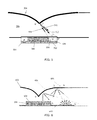
- Embodiments of the invention generally relate to illumination panels, and, more specifically, to coupling of light sources to waveguides.
- FIG. 1 illustrates such an illumination system 100 fabricated by coupling a discrete light source, e.g., a light-emitting diode (“LED”) 102 to a narrow face 104 of a waveguide 106 .
- a discrete light source e.g., a light-emitting diode (“LED”) 102
- LED light-emitting diode
- a waveguide 106 having a refractive index of N 1.5
- an LED 102 having Lambertian output characteristics combined as in the illumination system 100 , have a theoretical maximum coupling efficiency limit of 85%. That is, at most 85% of the light emitted by the LED 102 will be trapped within the waveguide 106 , and the remaining portion of the emitted light will be lost.
- This coupling inefficiency may be attributed to the constraints inherent in the side-emitting LED design of the illumination system 100 . While thinner waveguides are desirable, the thickness t of the waveguide must be larger than the width d of the LED in order to achieve coupling efficiencies approaching 85%. Relatively high coupling efficiencies (e.g., greater than approximately 70%) are difficult to obtain for cases where the thickness t of the waveguide is smaller than the width d of the LED. Thus, as waveguides become thinner, the coupling efficiency of the waveguide decreases and more light is lost. The coupling inefficiency may even set a practical lower bound on the thickness of the waveguide 106 . In addition, many side-emitting illumination systems utilize specially engineered LED and waveguide structures in order to increase the coupling efficiency. These structures not only add to the complexity and cost of the illumination system 100 but also increase its thickness.
- the present invention enables superior coupling efficiencies between light sources such as LEDs and thin waveguides by utilizing an LED that is embedded inside a waveguide and emits all its light inside the waveguide.
- a first portion of the emitted light propagates through the waveguide because its emission angle (with respect to the waveguide's upper surface) results in total internal reflection (“TIR”) of the first portion.
- TIR total internal reflection
- a second portion of the light is not emitted at an angle to the waveguide's upper (and/or lower) surface resulting in total internal reflection; this second portion may be reflected by a specular mirror positioned above the LED. The light thus reflected also undergoes total internal reflection, improving the coupling efficiency to the waveguide.
- Embodiments of the invention enable the waveguide to have a small thickness, e.g., less than approximately 1 mm, with an LED having a width of approximately 1 mm. Moreover, embodiments of the invention also utilize standard waveguide shapes and standard LED light sources not engineered to re-reflect emitted light, thereby reducing the cost and complexity of the system.
- top-emitting e.g., Lambertian
- side-emitting LEDs e.g., side-emitting LEDs
- Such chips may be placed below the waveguide instead of attached to a narrow side of the waveguide.
- a mirror may be used that exhibits specular reflection instead of a mirror exhibiting total internal reflection or a diffuser (i.e., a surface exhibiting diffuse reflection).
- the mirror may be positioned and designed such that most of the light emitted from the LED, e.g., more than approximately 85%, is coupled to the waveguide.
- the light reflected by the mirror may be within the propagation angle of the waveguide after reflection. Back-reflection of light toward the LED may be prevented, thereby obviating the need for specially engineered increased reflectivity of the LED surface (or the surface of the LED electrode) to decrease light absorption by the LED.
- the waveguide and LED may be included in a full illumination device featuring in-coupling, concentration, propagation, and out-coupling regions. Light propagating inside the waveguide in a direction away from the out-coupling region may be redirected toward the out -coupling region by a specially engineered shape of the waveguide's back edge.
- a top mirror may be included to reduce or prevent reflection of light back toward the LED in the vertical direction; a concentrating mirror may also be included (on, e.g., the back surface of the waveguide) to reduce or prevent reflection of light back toward the LED in the horizontal direction.
- the full illumination device may provide efficient (e.g., greater than approximately 70% or even 85% or more) light in-coupling to a thin waveguide, even when the thickness of the waveguide is approximately equal to (or even less than) the LED width.
- an illumination structure in general, in a first aspect, includes a waveguide and a discrete light source disposed proximate a bottom surface of the waveguide.
- a top[mirror is disposed above the discrete light source.
- the top mirror may be a curved mirror, semi-curved mirror, broken-line mirror, and/or single-line top mirror. A portion of a top surface of the sub-assembly module may not be covered by the discrete light source. Light emitted by the discrete light source may be reflected by the top mirror away from a top surface of the sub-assembly module and into a confined mode of the waveguide.
- the sub-assembly module may include a printed-circuit board and/or a carrier plate. In some embodiments, the sub-assembly module includes an index-matching region, one or more electrical interfaces with the discrete light source, and/or one or more mechanical interfaces with the discrete light source.
- the top mirror which may be a cone, pyramid, specular reflector, and/or have a substantially parabolic shape, may be positioned such that light from the discrete light source that does not strike the top mirror is within a confined mode of the waveguide. Alternatively or in addition, the top mirror may be positioned asymmetrically relative to the discrete light source.
- the top mirror may be positioned such that light from the discrete light source that does not strike the top mirror is within a confined mode of the waveguide.
- the illumination device may include one or more additional discrete light sources, such as RGB light sources, and they may be arranged in a line.
- the top mirror which may include a prism or triangular prism, may be disposed above two or more of the discrete light sources.
- a thickness of the waveguide may be approximately equal to, or less than, a width of the discrete light source.
- a flat mirror may be disposed proximate a top surface of the waveguide and proximate the top mirror.
- a diffuse mirror may be proximate a bottom surface of the waveguide, and light emitted by the discrete light source may be reflected by the flat mirror toward the diffuse mirror.
- a phosphor layer may be disposed above the discrete light source, and the discrete light source and the phosphor layer may be disposed within a notch in the bottom surface of the waveguide.
- An absorber may be disposed over the top mirror in a first region of the waveguide, and the absorber may have an absorbance such that light passing through the top mirror and the absorber has an intensity approximately equal to an intensity of light passing through a top waveguide surface in a second region of the waveguide proximate the first region of the waveguide.
- a method for coupling light emitted from a discrete light source to a waveguide includes emitting light from a discrete light source disposed proximate a bottom surface of the waveguide. A portion of the emitted light is reflected from a top mirror disposed above the discrete light source, thereby confining the reflected portion of the emitted light to propagate in the waveguide. A second portion of the emitted light may be reflected from a diffusive mirror disposed proximate a bottom surface of the waveguide, thereby allowing the reflected second portion of the emitted light to propagate in the waveguide.
- illumination structure includes a plurality of panels.
- Each panel includes an in-coupling and out-coupling region.
- the in-coupling region includes a discrete light source and a horizontal mirror and the out-coupling region is disposed proximate the in-coupling region.
- Light emitted by the discrete light source is reflected by the horizontal mirror into the out-coupling region, and the light is emitted over substantially all of a surface of the out -coupling region.
- the out-coupling region of one panel may be disposed over the in-coupling region of another panel, thereby forming a substantially uniform light-emission surface. Substantially no light reflected by the horizontal mirror into the out-coupling region may reflect back toward the discrete light source.
- FIG. 1 is a cross-sectional view of a prior-art side-mounted illumination system
- FIG. 2 is a cross-sectional view of an illumination system featuring a parabolic mirror
- FIG. 3 is a cross-sectional view of an illumination system showing relative dimensions
- FIG. 4 is a cross-sectional view of an illumination system with an embedded LED
- FIG. 5 is a cross-sectional view of an illumination system featuring an LED sub-assembly
- FIG. 6 is a cross-sectional view of an illumination system featuring a bottom diffusive mirror
- FIG. 7 is a cross-sectional view of an illumination system featuring an alternative mirror design
- FIG. 8 is a plan view of an illumination panel for use in a tiled configuration of panels
- FIG. 9 is a plan view of an in-coupling region featuring elliptical mirror sections
- FIG. 10 is a plan view of an illumination panel featuring multiple LEDs
- FIG. 11 is a plan view of an illumination panel featuring multiple LEDs in an alternate configuration
- FIG. 12 is a cross-sectional view of an illumination panel
- FIG. 13 is a plan view of an illumination panel featuring scattering structures
- FIG. 14 is a cross-sectional view of an illumination panel featuring two layers
- FIGS. 15A and 15B are a perspective view and a plan view, respectively, of an illumination panel featuring multiple LEDs;
- FIG. 16 is a cross-sectional view of an illumination panel featuring an asymmetrically placed LED
- FIG. 17 is a cross-sectional view of an illumination panel featuring a phosphor layer.
- FIGS. 18A and 18B are a cross-sectional view and top view, respectively, of an illumination panel.
- Embodiments of the invention apply to two different cases: (1) when a thickness, t, of the waveguide is approximately equal to or larger than the width, d, of the light source and (2) when t is less than d.
- a curved, semi-curved, broken-line, or single-line top mirror redirects light that strikes it into confined modes (i.e., propagation paths confined by the waveguide).
- curved refers to a mirror with a curved shape
- si-curved refers to a mirror with a curved segment and straight segments
- broken-line refers to a mirror having several discrete straight segments that approximate a curved segment
- single-line refers to a mirror consisting of a straight segment.
- the mirror is positioned such that light propagating at an angle less than necessary for TIR (and which therefore will not be confined within the waveguide) strikes the mirror.
- the mirror shape and position may enable the redirection of light from unconfined modes into confined modes. Any light already in a confined mode that does strike the mirror may remain in a confined mode after reflection.
- FIG. 2 illustrates one example of a parabolic mirror 202 that is set around a point A (the top-right corner 204 of an LED 206 ), such that the light rays emitted from the point A toward the region of the mirror bounded by points M and D (“region M-D”) are reflected back into the waveguide 208 at an angle equal to (or larger than) the critical angle ⁇ T for total internal reflection.
- region A-B all of the light rays from the portion of the top surface 210 of the LED 206 bounded by points A and B
- region A-B may be reflected at angles larger than ⁇ T so as to be confined.
- the light rays from the region bounded by points B and C (“region B-C”) may undergo one or multiple reflections at the mirror such that their final propagating angle is also greater than ⁇ T .
- Light rays that do not strike the mirror are, by definition, already confined (i.e., propagating at an angle greater than ⁇ T ) because the light ray from point A to point M and the light ray from point A to point D propagate at an angle ⁇ T .
- the light ray from point A to point M propagates perpendicularly to the surface of the mirror 202 at point M such that the light is reflected back toward point A.
- the mirror 202 is substantially parallel to the plane of the waveguide 208 , and the light ray propagating from point A at an angle ⁇ T is reflected into the waveguide 208 at an angle ⁇ T (pursuant to Snell's Law).
- the light rays may act similarly if one or more cladding layers (not shown) are added to the waveguide 208 .
- FIG. 3 depicts an exemplary embodiment of the invention that includes relative dimensions.
- the waveguide 208 thickness t (as measured from the top surface 210 of the LED 206 to the top surface 302 of the waveguide 208 ) may be approximately equal to the LED 206 width d.
- the mirror configuration takes alignment tolerances into account.
- the width d of the LED 206 and the thickness t of the waveguide 208 may thus be defined as ⁇ square root over (2) ⁇ y 0
- the shortest distance between the mirror 304 and the surface 210 (at point M of the mirror 304 ) is y 0 / ⁇ square root over (2) ⁇ .
- point M of the mirror 304 is defined with reference to point A (the right edge of the LED 206 )
- slight misalignment of the LED 206 may lead to less efficient light coupling.
- the sensitivity to such misalignment may be reduced by positioning point M with respect to a point A′ offset from point A by a typical misalignment tolerance, e.g., approximately 0.1 mm.
- light emitted by or through side faces 412 of the LED 206 may be coupled into the waveguide 208 .
- the LED 206 may be embedded within the waveguide 208 , as shown, which then may have a thickness of approximately t+h (i.e., slightly larger than the LED width d).
- the light from an LED 206 having a width d of approximately 1 mm may be coupled to a waveguide 208 having a thickness of approximately 1 mm (or slightly greater than approximately 1 mm) while achieving a coupling efficiency greater than approximately 85%, or even greater than approximately 95%.
- Light emitted from a side surface 412 of the LED 206 may propagate at angles less than the angle required for total internal reflection.
- a reflecting layer 402 may therefore be placed at the bottom facet 404 of the waveguide 208 , at least spanning and desirably extending beyond the perimeter of the LED 206 , to capture the unconfined light.
- the reflecting layer 402 may reflect unconfined light toward the top mirror 304 .
- the position of point D may be determined by the ray 416 from point S′ that strikes the waveguide 298 top surface at an incident angle equal to the critical angle ⁇ T .
- the distance between points S and S′ may be approximately equal to the thickness h of the LED 206 .
- the non-zero thickness h of the LED 206 is considered when designing the shape and placement of the mirror 202 . This consideration is important for LEDs that not only emit light from their top surfaces 210 (as in the case described above), but also from their side surfaces 412 . The light emitted from or through the side surfaces 412 of the LED 206 may also be confined in the waveguide 208 .
- the critical angle ⁇ T is determined by the ray from point S (the bottom-right corner 414 of the LED 206 ) to point D.
- ⁇ T will be slightly larger than the ⁇ T described above (which may apply to an LED that emits light only from its top surface). This selection of the proper ⁇ T enables the coupling of substantially all light emitted from the LED 206 .
- the critical angle ⁇ T (measured from point A) is approximately 45 degrees.
- FIG. 5 illustrates an LED light source 206 assembled on a top surface of an LED sub-assembly module 502 , such as a printed-circuit board (“PCB”) or a carrier plate, which provides a mechanical interface to hold the LED light source 206 in position and/or an electrical interface to operate the LED light source 206 .
- an index-matching material 504 may be used to fill the space between the LED 206 and the top mirror 304 , thereby providing an optical connection not only between the LED 206 and the top mirror 304 but also between the top mirror 304 and the top surface 506 of the LED sub-assembly 502 .
- the top surface 506 of the LED sub-assembly 502 may extend beyond the dimensions of the LED light source 206 , thus allowing guided light rays to reach the top surface 506 of the LED sub-assembly 502 .
- the reflectivity quality of the LED sub-assembly surface 506 may not be controllable and is less than the TIR reflectivity. Therefore, the top mirror 304 positioned over the LED light source 206 is preferably designed to reflect light away from the LED sub-assembly 502 . In one embodiment, as shown in FIG. 5 , the top mirror 304 has a parabolic contour.
- a light ray 508 is coupled from a point S at the right edge 510 of the LED light source 206 , reflected from a point M on the top mirror 304 , and radiates back along a path 510 to a point S′′ at the end of the index-matching region 504 of the LED sub-assembly 502 .
- Other rays emitted from the LED light source may be reflected past the LED sub-assembly 502 to the region beyond point S′′.
- Point S′ which is approximately halfway between points S and S′′, may be used as a reference point for forming the parabolic shape of the top mirror 504 .
- a light ray 512 emitted from point S′ that strikes the top mirror at point M may be reflected back toward point S′.
- the shape of the top mirror 304 at point M may a sharp edge or a curve.
- the width of the top mirror 304 is 2 mm
- the shape of the top mirror 304 at point M may be a curve having a radius of 0.1 mm. Such a shape may decrease the manufacturing cost and/or complexity of the top mirror 304 relative to the cost and complexity of manufacturing a sharp edge at point M without significantly affecting the performance of the top mirror 304 .
- all the unconfined light rays strike a curved, semi-curved, or broken-line top mirror that redirects the light back into the waveguide.
- the mirror preferably does not reflect the light back into the LED. While most of these reflected rays are redirected to confined modes (i.e., propagation paths confined by the waveguide), some remain propagating at angles below the critical angle (i.e., they remain unconfined modes). These unconfined modes may be redirected toward a bottom diffusive reflector which redirects at least a significant portion (for example, greater than 55%) of this remaining light into confined modes.
- FIG. 6 depicts a top specular mirror 602 including a curved section 604 between points M and D and a flat section 606 between points D and E.
- the flat section 606 may be substantially parallel to a top surface 608 of the LED 206 .
- a bottom diffusive mirror 610 extends from approximately the LED 206 edge A to a point G and may be designed so that most or all of the reflected light already corresponding to confined modes does not strike the bottom diffusive mirror 610 .
- a similar bottom diffusive mirror may be disposed on the other side of the LED 206 .
- Light emitted from the LED 206 that does not strike the curved section 604 may instead strike the flat section 606 and be reflected toward the bottom diffusive mirror 610 . This light, initially in an unconfined mode, strikes the diffusive mirror 610 and is reflected into confined modes. Coupling efficiencies greater than approximately 80% may be obtained with this configuration.
- FIG. 7 depicts an embodiment in which the curved section 604 of the mirror 602 has a radius approximately equal to half the width of the LED 206 (i.e., d/2), and point M of the mirror approximately coincides with point B (the center of the top surface 608 of the LED 206 ).
- Light rays from point A that propagate toward the curved section 604 are reflected back toward point A.
- Light rays from point B propagating at approximately 45 degrees strike the top mirror 602 at point D and are reflected to point G of the diffusive mirror 610 .
- most or all of the unconfined modes emitted from the LED 206 between points A and B strike the diffusive mirror 610 and are reflected into confined modes.
- large illumination structures are formed by arranging (or “tiling”) panels that include the above-described waveguide structures.
- each panel may include or consist essentially of an input region and an output region, and the output region of one panel may cover the input region of an adjoining panel.
- a large illumination structure is formed by placing panels adjoining each other (i.e., in a non-tiled configuration with no overlap between panels) such that light is coupled out from the entire panel surface.
- FIG. 8 illustrates a panel 802 for use in a tiled configuration of one or more panels.
- the output region 804 of each panel 802 may include scattering structures (such as hemispheres, wedges, particles, and/or other similar structures).
- Light from an LED 806 disposed in an input region 808 is preferably directed toward the output region 804 such that the light does not pass through the LED 806 and/or a top mirror.
- Light rays 810 emitted by the LED 806 away from the output region 804 may be reflected back toward the output region 804 by a back horizontal mirror 812 .
- the back horizontal mirror 812 is not perfectly linear, but rather is formed of one or two elliptical mirror sections.
- FIG. 9 shows, in one embodiment, elliptical mirror sections 906 , 908 each define a portion of the back horizontal mirror 812 .
- the LED 806 may be positioned approximately at a position corresponding to the poles common to each ellipse 906 , 906 (which also have poles 902 , 904 ). Thus, substantially all of the light rays emitted from the LED 806 may be redirected (and distributed) to the output coupling region 804 while not passing through the LED 806 .
- emission of white light e.g., formed by the combination of red, green, and blue (“RGB”) light
- RGB red, green, and blue
- each single LED of the above-described embodiments may be replaced by a set of at least three LEDs: at least one emitting red light, at least one emitting green light, and at least one emitting blue light.
- FIG. 10 illustrates an embodiment in which a plurality of LEDs 1002 are “crowded” (i.e., arranged close together, but not necessarily collinearly), such that color mixing is optimized and the loss due to light propagating from one LED directly to the other LEDs is minimal.
- the LEDs may include a red LED 1004 , a green LED 1006 , and a blue LED 1008 .
- separate horizontal back mirrors 1102 , 1104 , 1106 are provided for each LED 1004 , 1006 , 1008 , respectively, and the colors are mixed to white light while propagating in the input region (i.e., before the light reaches the output region 804 ).
- FIG. 12 illustrates a side view of a panel 1202 including an LED 1204 disposed on a substrate 1206 .
- light is preferably emitted from the entire top surface 1208 of the panel 1202 , including the region 1210 above the top curved mirror 1212 .
- the intensity of the light emitted through the top curved mirror 1212 is equal to the intensity of the light coupled out from the rest of the top surface 1208 of the panel 1202 .
- a suitable absorber 1214 may be placed above the top curved mirror 1212 to emit light of a desired intensity therefrom.
- Some light may penetrate through the top curved mirror 1212 .
- the absorber 1214 should absorb ⁇ 98% of the light intensity.
- the absorber 1214 is diffusive.
- scattering structures 1216 may be placed across some or all of a top surface 1208 of the panel 1202 to aid in the out-coupling of light.
- a mirror 1218 may placed at the bottom surface 1220 of the panel 1202 .
- the LEDs may be crowded (i.e., positioned closely together) to permit the use of a single out-coupling structure for all of the LEDs.
- the density of scattering structures preferably increases as a function of distance away from the LEDs.
- scattering structures with increasing scattering coefficients may be utilized.
- the region above the top curved mirror of one LED may be transparent to light emitted by the other LEDs in order to facilitate out-coupling of light of all colors.
- FIGS. 13 and 14 depict a suitable configuration.
- FIG. 13 depicts a top view of an isolated illumination panel 1302 that includes four crowded LEDs 1304 (e.g., one red, two green, and one blue—“RGGB”). Out-coupling scattering structures 1306 are provided between and/or around the LEDs 1304 .
- a cross-sectional view of two of the LEDs 1304 , including a red LED 1402 and a blue LED 1404 , and their corresponding upper curved mirrors 1406 , 1408 is shown in FIG. 14 .
- a top layer 1410 of the waveguide disposed above the upper curved mirrors 1406 , 1408 includes scattering structures 1412 for facilitating the out-coupling of light in the regions above the upper curved mirrors 1406 , 1408 .
- the top layer 1410 is preferably optically connected with the bottom layer 1414 (the layer containing the curved mirrors 1406 , 1408 and the LEDs 1402 , 1404 ) such that light freely propagates from one layer to the other.
- the scattering structures 1412 may be disposed at the top surface 1416 of the top layer 1410 . In other embodiments, the scattering structures 1412 are incorporated in other portions of the top layer 1410 , or even in the bottom layer 1414 .
- FIG. 14 also depicts several different light rays, each traveling a different path from an LED 1402 , 1404 to emission from the waveguide 1418 .
- Ray (a) is emitted from the blue LED 1404 and scattered from the blue top curved mirror 1408 into the waveguide 1418 .
- Ray (b) is the part of ray (a) that penetrates through the mirror 1408 and is emitted from the waveguide 1418 by the scattering structures 1412 .
- Ray (c) is emitted from the red LED 1402 and then from the waveguide 1418 through the scattering structures 1412 .
- Ray (d) is the part of ray (c) that is reflected back to the waveguide 1418 and, after reflection therefrom, is emitted from the waveguide 1418 in the region above the blue top curved mirror 1408 .
- each LED has its own, separate top mirror.
- each top mirror is shaped like a cone, pyramid, or any other non-flat shape suitable to retaining light within the waveguide that would otherwise escape.
- more than one of the LEDs share a single top mirror.
- the LEDs may be arranged in a line, and the shared top mirror may be shaped like a prism with curved side facets.
- the shared top mirror 1502 is a triangular prism having triangular side facets and the array of LEDs 1504 includes RRGGB LEDs.
- the top curved mirror 1502 is not limited to symmetric structures; it may be designed asymmetrically if, for example, the LEDs 1504 are configured asymmetrically, such as an LED not located at the center of the LED sub-assembly 1506 . In such a case, in order to avoid rays striking the LED sub-assembly (as illustrated in FIG. 5 ), the top curved mirror 1502 may be designed asymmetrically and/or located asymmetrically (relative to the center of the LEDs 1504 ). An example is shown in FIG.
- the LED sub-assembly 1602 is asymmetric (relative to the center of the LED 1604 ) and, accordingly, the top curved mirror 1606 is asymmetrically located (relative to the center of the LED 1604 ).
- the curved mirror 1606 is located such that rays from point A are reflected back from point M toward point A and rays from point C are reflected from point M toward point C′.
- a virtual point C′′ is located approximately at the center between point C and point C′; i.e., virtual rays from point C′′ striking point M will be back reflected to point C′′.
- point M is located at the center between points A and C′′.
- FIG. 17 illustrates a side view of a waveguide 1702 that features a phosphor layer 1704 .
- the phosphor layer 1704 may produce white light from a single-color LED light source 1706 .
- the phosphor layer 1704 preferably converts some of the light from the LED 1706 to another wavelength. The original light adds to the converted light, creating white light. For example, a blue LED may be combined with a yellow phosphor layer, and the blue light from the LED may combine with the yellow light from the phosphor layer to produce white light.
- phosphors are utilized to facilitate the emission of white light (or light of another preferred wavelength).
- the configuration depicted in FIG. 17 includes a patterned waveguide 1702 and an LED chip 1716 with matching indices of refraction.
- the waveguide may be an optical polymer, e.g., a polymethyl methacrylate (PMMA), and may include a bottom notch 1720 (for embedding the LED 1716 therein) and a top curved mirror 1708 .
- PMMA polymethyl methacrylate
- the waveguide 1702 may be formed by molding or by another suitable process known in the art.
- the waveguide 1702 may also include a bottom mirror 1712 .
- the LED chip 1716 may be mounted into the waveguide notch 1720 such that it substantially seals the notch 1720 along the bottom surface 1722 of the waveguide 1702 .
- any remaining space in the notch 1720 may be filled with an index-matching material 1718 having an index of refraction matching that of the waveguide 1702 .
- the phosphor layer 1704 may be formed above or around the LED chip 1716 , or it may be deposited directly in the waveguide notch 1720 prior to introduction of the LED chip 1716 .
- An absorber layer 1710 and a substrate 1714 may also be included.
- FIGS. 18A and 18B depict a side and top view, respectively, of an isolated panel configuration 1800 , including a phosphor layer, that adds scattering structures 1802 .
- the illumination system 1800 may be utilized in cases where the waveguide 1702 thickness is either approximately equal to (or even larger than) the width of the LED 1716 , as well as in cases where the waveguide thickness is less than the LED width.
- the phosphor-containing system may also be utilized in tiled or isolated configurations, as described above.
Abstract
Description
Claims (34)
Priority Applications (10)
| Application Number | Priority Date | Filing Date | Title |
|---|---|---|---|
| US12/500,889 US8301002B2 (en) | 2008-07-10 | 2009-07-10 | Slim waveguide coupling apparatus and method |
| US12/715,880 US8297786B2 (en) | 2008-07-10 | 2010-03-02 | Slim waveguide coupling apparatus and method |
| US13/606,202 US8851712B2 (en) | 2008-07-10 | 2012-09-07 | Slim waveguide coupling apparatus and method |
| US14/478,444 US9164218B2 (en) | 2008-07-10 | 2014-09-05 | Slim waveguide coupling apparatus and method |
| US14/849,933 US9470837B2 (en) | 2008-07-10 | 2015-09-10 | Slim waveguide coupling apparatus and method |
| US15/269,231 US9606288B2 (en) | 2008-07-10 | 2016-09-19 | Slim waveguide coupling apparatus and method |
| US15/432,490 US9798077B2 (en) | 2008-07-10 | 2017-02-14 | Slim waveguide coupling apparatus and method |
| US15/710,940 US9983351B2 (en) | 2008-07-10 | 2017-09-21 | Slim waveguide coupling apparatus and method |
| US15/963,685 US10989863B2 (en) | 2008-07-10 | 2018-04-26 | Slim waveguide coupling apparatus and method |
| US17/215,107 US11231547B2 (en) | 2008-07-10 | 2021-03-29 | Slim waveguide coupling apparatus and method |
Applications Claiming Priority (3)
| Application Number | Priority Date | Filing Date | Title |
|---|---|---|---|
| US7958208P | 2008-07-10 | 2008-07-10 | |
| US20608009P | 2009-01-27 | 2009-01-27 | |
| US12/500,889 US8301002B2 (en) | 2008-07-10 | 2009-07-10 | Slim waveguide coupling apparatus and method |
Related Child Applications (1)
| Application Number | Title | Priority Date | Filing Date |
|---|---|---|---|
| US12/715,880 Continuation-In-Part US8297786B2 (en) | 2008-07-10 | 2010-03-02 | Slim waveguide coupling apparatus and method |
Publications (2)
| Publication Number | Publication Date |
|---|---|
| US20100008628A1 US20100008628A1 (en) | 2010-01-14 |
| US8301002B2 true US8301002B2 (en) | 2012-10-30 |
Family
ID=41505250
Family Applications (1)
| Application Number | Title | Priority Date | Filing Date |
|---|---|---|---|
| US12/500,889 Active 2030-12-02 US8301002B2 (en) | 2008-07-10 | 2009-07-10 | Slim waveguide coupling apparatus and method |
Country Status (1)
| Country | Link |
|---|---|
| US (1) | US8301002B2 (en) |
Cited By (31)
| Publication number | Priority date | Publication date | Assignee | Title |
|---|---|---|---|---|
| US20100253770A1 (en) * | 2009-04-02 | 2010-10-07 | Samsung Electronics Co., Ltd. | Immunoassay apparatus and method of determining brightness value of target area on optical image using the same |
| US20120257415A1 (en) * | 2007-12-19 | 2012-10-11 | Noam Meir | Planar white illumination apparatus |
| US20140211503A1 (en) * | 2013-01-30 | 2014-07-31 | Cree, Inc. | Waveguide bodies including redirection features and methods of producing same |
| US20140355302A1 (en) * | 2013-03-15 | 2014-12-04 | Cree, Inc. | Outdoor and/or Enclosed Structure LED Luminaire for General Illumination Applications, Such as Parking Lots and Structures |
| US9086551B2 (en) * | 2013-10-30 | 2015-07-21 | International Business Machines Corporation | Double mirror structure for wavelength division multiplexing with polymer waveguides |
| US9164218B2 (en) | 2008-07-10 | 2015-10-20 | Oree, Inc. | Slim waveguide coupling apparatus and method |
| US9291320B2 (en) | 2013-01-30 | 2016-03-22 | Cree, Inc. | Consolidated troffer |
| US9366799B2 (en) | 2013-03-15 | 2016-06-14 | Cree, Inc. | Optical waveguide bodies and luminaires utilizing same |
| US9366396B2 (en) | 2013-01-30 | 2016-06-14 | Cree, Inc. | Optical waveguide and lamp including same |
| US9389367B2 (en) | 2013-01-30 | 2016-07-12 | Cree, Inc. | Optical waveguide and luminaire incorporating same |
| US9625638B2 (en) | 2013-03-15 | 2017-04-18 | Cree, Inc. | Optical waveguide body |
| US9690029B2 (en) | 2013-01-30 | 2017-06-27 | Cree, Inc. | Optical waveguides and luminaires incorporating same |
| US9798072B2 (en) | 2013-03-15 | 2017-10-24 | Cree, Inc. | Optical element and method of forming an optical element |
| US9857519B2 (en) | 2012-07-03 | 2018-01-02 | Oree Advanced Illumination Solutions Ltd. | Planar remote phosphor illumination apparatus |
| US9869432B2 (en) | 2013-01-30 | 2018-01-16 | Cree, Inc. | Luminaires using waveguide bodies and optical elements |
| US10209429B2 (en) | 2013-03-15 | 2019-02-19 | Cree, Inc. | Luminaire with selectable luminous intensity pattern |
| US10416377B2 (en) | 2016-05-06 | 2019-09-17 | Cree, Inc. | Luminaire with controllable light emission |
| US10436970B2 (en) | 2013-03-15 | 2019-10-08 | Ideal Industries Lighting Llc | Shaped optical waveguide bodies |
| US10502899B2 (en) * | 2013-03-15 | 2019-12-10 | Ideal Industries Lighting Llc | Outdoor and/or enclosed structure LED luminaire |
| US20200064538A1 (en) * | 2018-08-24 | 2020-02-27 | Beijing Boe Optoelectronics Technology Co., Ltd. | Light guide plate and its fabricating method, as well as backlight module |
| US10739513B2 (en) | 2018-08-31 | 2020-08-11 | RAB Lighting Inc. | Apparatuses and methods for efficiently directing light toward and away from a mounting surface |
| US10801679B2 (en) | 2018-10-08 | 2020-10-13 | RAB Lighting Inc. | Apparatuses and methods for assembling luminaires |
| US11287105B2 (en) | 2020-02-07 | 2022-03-29 | Nichia Corporation | Light emitting module and planar light source |
| US11421856B2 (en) | 2020-01-31 | 2022-08-23 | Nichia Corporation | Light emitting module, surface light source, and a method of manufacturing light emitting module |
| US11480319B2 (en) | 2020-02-07 | 2022-10-25 | Nichia Corporation | Light emitting module and planar light source |
| US11480725B2 (en) | 2020-06-04 | 2022-10-25 | Nichia Corporation | Planar light source and method of manufacturing planar light source |
| US11506937B2 (en) | 2020-06-03 | 2022-11-22 | Nichia Corporation | Planar light source and method of manufacturing the same |
| US11520098B2 (en) | 2020-02-07 | 2022-12-06 | Nichia Corporation | Light emitting module and planar light source |
| US11598913B2 (en) | 2020-07-01 | 2023-03-07 | Nichia Corporation | Light-emitting module |
| US11719882B2 (en) | 2016-05-06 | 2023-08-08 | Ideal Industries Lighting Llc | Waveguide-based light sources with dynamic beam shaping |
| US11740401B2 (en) | 2020-08-31 | 2023-08-29 | Nichia Corporation | Method of manufacturing light emitting module |
Families Citing this family (28)
| Publication number | Priority date | Publication date | Assignee | Title |
|---|---|---|---|---|
| US8272758B2 (en) * | 2005-06-07 | 2012-09-25 | Oree, Inc. | Illumination apparatus and methods of forming the same |
| US8215815B2 (en) | 2005-06-07 | 2012-07-10 | Oree, Inc. | Illumination apparatus and methods of forming the same |
| WO2006131924A2 (en) | 2005-06-07 | 2006-12-14 | Oree, Advanced Illumination Solutions Inc. | Illumination apparatus |
| US7907804B2 (en) * | 2007-12-19 | 2011-03-15 | Oree, Inc. | Elimination of stitch artifacts in a planar illumination area |
| US20090225566A1 (en) * | 2008-03-05 | 2009-09-10 | Micha Zimmermann | Illumination apparatus and methods of forming the same |
| US20100098377A1 (en) * | 2008-10-16 | 2010-04-22 | Noam Meir | Light confinement using diffusers |
| US20100208469A1 (en) * | 2009-02-10 | 2010-08-19 | Yosi Shani | Illumination surfaces with reduced linear artifacts |
| US8624527B1 (en) | 2009-03-27 | 2014-01-07 | Oree, Inc. | Independently controllable illumination device |
| US20100320904A1 (en) * | 2009-05-13 | 2010-12-23 | Oree Inc. | LED-Based Replacement Lamps for Incandescent Fixtures |
| WO2010150202A2 (en) | 2009-06-24 | 2010-12-29 | Oree, Advanced Illumination Solutions Inc. | Illumination apparatus with high conversion efficiency and methods of forming the same |
| US8591072B2 (en) | 2011-11-16 | 2013-11-26 | Oree, Inc. | Illumination apparatus confining light by total internal reflection and methods of forming the same |
| US9110281B2 (en) * | 2011-12-22 | 2015-08-18 | Qualcomm Mems Technologies, Inc. | Vertically etched facets for display devices |
| DE102013106689B4 (en) | 2013-06-26 | 2022-02-03 | OSRAM Opto Semiconductors Gesellschaft mit beschränkter Haftung | Optoelectronic semiconductor component |
| US9651740B2 (en) | 2014-01-09 | 2017-05-16 | Cree, Inc. | Extraction film for optical waveguide and method of producing same |
| FR3026816A1 (en) * | 2014-10-01 | 2016-04-08 | Valeo Vision | LIGHTING SYSTEM FOR MOTOR VEHICLE |
| WO2016190937A1 (en) * | 2015-03-09 | 2016-12-01 | Massachusetts Institute Of Technology | Phosphor-loaded waveguide |
| CN106764473A (en) * | 2015-11-24 | 2017-05-31 | 欧普照明股份有限公司 | A kind of LED illumination module |
| CN109148674B (en) * | 2017-06-28 | 2023-05-16 | 日亚化学工业株式会社 | Light emitting device |
| JP6801695B2 (en) * | 2018-08-03 | 2020-12-16 | 日亜化学工業株式会社 | Light emitting module and its manufacturing method |
| JP6717400B2 (en) * | 2018-08-03 | 2020-07-01 | 日亜化学工業株式会社 | Light emitting module |
| CN110794614B (en) * | 2018-08-03 | 2022-10-25 | 日亚化学工业株式会社 | Light emitting module |
| JP6729646B2 (en) * | 2018-08-21 | 2020-07-22 | 日亜化学工業株式会社 | Light emitting device |
| DE102018218441A1 (en) * | 2018-10-29 | 2020-04-30 | Volkswagen Aktiengesellschaft | Surface lighting element and interior equipment element for a motor vehicle with a surface lighting element |
| JP6680349B1 (en) * | 2018-12-28 | 2020-04-15 | 日亜化学工業株式会社 | Light emitting module |
| JP6866903B2 (en) * | 2019-03-05 | 2021-04-28 | 日亜化学工業株式会社 | Luminous module |
| JP6841292B2 (en) | 2019-03-05 | 2021-03-10 | 日亜化学工業株式会社 | Luminous module |
| US11061178B2 (en) * | 2019-03-05 | 2021-07-13 | Nichia Corporation | Light emitting module |
| JP7001945B2 (en) * | 2020-11-25 | 2022-01-20 | 日亜化学工業株式会社 | Light emitting module and its manufacturing method |
Citations (325)
| Publication number | Priority date | Publication date | Assignee | Title |
|---|---|---|---|---|
| GB512062A (en) | 1938-01-28 | 1939-08-29 | Ernst Hirsch | Improvements in reflectors |
| US3261356A (en) | 1963-10-21 | 1966-07-19 | American Cystoscope Makers Inc | Suction and illumination device |
| US3626471A (en) | 1969-10-13 | 1971-12-07 | Robert E Florin | Illuminated suction brain retractor |
| US3871747A (en) | 1972-10-03 | 1975-03-18 | Us Navy | Optical waveguide display panel |
| US3995934A (en) | 1973-10-19 | 1976-12-07 | Nath Guenther | Flexible light guide |
| US4551129A (en) | 1983-04-08 | 1985-11-05 | Coleman D Jackson | Technique and apparatus for intraocular and microsurgery including lighter-irrigator hypodermic tube |
| US4669467A (en) | 1985-03-22 | 1987-06-02 | Massachusetts Institute Of Technology | Mode mixer for a laser catheter |
| US4714983A (en) | 1985-06-10 | 1987-12-22 | Motorola, Inc. | Uniform emission backlight |
| US4762381A (en) | 1986-01-29 | 1988-08-09 | Sumitomo Electric Industries, Ltd. | Optical element integrated optical waveguide and production of the same |
| US4783140A (en) | 1985-03-30 | 1988-11-08 | Sumitomo Electric Industries, Ltd. | Elastomeric optical waveguide with core and cladding imparted with elasticity by irradiation of a radioactive ray |
| US4829192A (en) | 1986-03-27 | 1989-05-09 | Kabushiki Kaisha Tokai Rika Denki Seisakusho | Photo-coupler with delay function using a fluorescent substance as the delay means |
| US4853593A (en) | 1986-09-30 | 1989-08-01 | Siemens Aktiengesellschaft | Light emitting diode (LED) display |
| US4872837A (en) | 1987-02-06 | 1989-10-10 | Robert Issalene | Surgical or dental instrument and cannulae for aspirating, cleaning, drying and illuminating |
| US4878072A (en) | 1987-09-11 | 1989-10-31 | Oce-Nederland B.V. | LED age correction means |
| US4903172A (en) | 1987-09-11 | 1990-02-20 | Schoeniger Karl Heinz | Display construction |
| US4906062A (en) | 1988-10-26 | 1990-03-06 | The General Electric Company, P.L.C. | Integrated optical waveguide bend |
| US5009483A (en) | 1989-04-12 | 1991-04-23 | Rockwell Iii Marshall A | Optical waveguide display system |
| US5048913A (en) | 1989-12-26 | 1991-09-17 | United Technologies Corporation | Optical waveguide embedded transverse spatial mode discrimination filter |
| US5061032A (en) | 1989-12-26 | 1991-10-29 | United Technologies Corporation | Optical waveguide embedded light redirecting and focusing bragg grating arrangement |
| US5139420A (en) | 1990-09-04 | 1992-08-18 | Walker William S | Dental mirror system |
| US5152686A (en) | 1991-04-25 | 1992-10-06 | Calvin Duggan | Dental appliance |
| US5165187A (en) | 1987-01-30 | 1992-11-24 | Fiber Sense & Signals Inc. | Edge illuminated sign panel |
| US5211467A (en) | 1992-01-07 | 1993-05-18 | Rockwell International Corporation | Fluorescent lighting system |
| US5281134A (en) | 1991-11-19 | 1994-01-25 | Schultz Allen J | Fiber optic illumination system for dental instruments |
| US5425730A (en) | 1994-02-16 | 1995-06-20 | Luloh; K. P. | Illumination cannula system for vitreous surgery |
| US5535105A (en) | 1992-08-05 | 1996-07-09 | Koenen; H. Peter | Work glove and illuminator assembly |
| US5559358A (en) | 1993-05-25 | 1996-09-24 | Honeywell Inc. | Opto-electro-mechanical device or filter, process for making, and sensors made therefrom |
| US5569254A (en) | 1995-04-12 | 1996-10-29 | Midas Rex Pneumatic Tools, Inc. | Surgical resection tool having an irrigation, lighting, suction and vision attachment |
| US5580154A (en) | 1994-08-24 | 1996-12-03 | Coulter; James D. | Glow-in-the-dark glove apparatus |
| US5596671A (en) | 1994-04-28 | 1997-01-21 | Rockwell, Iii; Marshall A. | Optical waveguide display system |
| US5675678A (en) | 1995-10-10 | 1997-10-07 | Ceram Optec Industries Inc. | Flexible system for linearly distributed illumination |
| US5718666A (en) | 1996-02-29 | 1998-02-17 | Bioenterics Corporation | Transilluminating bougie |
| JPH10247412A (en) | 1997-03-03 | 1998-09-14 | Omron Corp | Surface light source device |
| US5813752A (en) | 1997-05-27 | 1998-09-29 | Philips Electronics North America Corporation | UV/blue LED-phosphor device with short wave pass, long wave pass band pass and peroit filters |
| US5813753A (en) | 1997-05-27 | 1998-09-29 | Philips Electronics North America Corporation | UV/blue led-phosphor device with efficient conversion of UV/blues light to visible light |
| US5847507A (en) | 1997-07-14 | 1998-12-08 | Hewlett-Packard Company | Fluorescent dye added to epoxy of light emitting diode lens |
| US5899552A (en) | 1993-11-11 | 1999-05-04 | Enplas Corporation | Surface light source device |
| US5947588A (en) | 1997-10-06 | 1999-09-07 | Grand General Accessories Manufacturing Inc. | Light fixture with an LED light bulb having a conventional connection post |
| US5959316A (en) | 1998-09-01 | 1999-09-28 | Hewlett-Packard Company | Multiple encapsulation of phosphor-LED devices |
| US5969869A (en) | 1996-10-25 | 1999-10-19 | Asahi Kogaku Kogyo Kabushiki Kaisha | Prism |
| US6016038A (en) | 1997-08-26 | 2000-01-18 | Color Kinetics, Inc. | Multicolored LED lighting method and apparatus |
| GB2339318A (en) | 1998-07-06 | 2000-01-19 | Lite On Electronics Inc | Lateral type backlight using light emitting diodes |
| US6031511A (en) | 1997-06-10 | 2000-02-29 | Deluca; Michael J. | Multiple wave guide phosphorous display |
| GB2343361A (en) | 1998-11-05 | 2000-05-10 | Paul Spooner | A glove with illuminating light |
| US6079838A (en) * | 1995-06-27 | 2000-06-27 | Lumitex, Inc. | Light emitting panel assemblies |
| US6097871A (en) | 1994-08-26 | 2000-08-01 | De Dobbelaere; Peter Martin Cyriel | Method of making an optical waveguide to fibre connector using a free-standing, flexible waveguide sheet |
| US6155699A (en) | 1999-03-15 | 2000-12-05 | Agilent Technologies, Inc. | Efficient phosphor-conversion led structure |
| US6226440B1 (en) | 1996-09-16 | 2001-05-01 | Whelen Engineering Company, Inc. | Optical coupler and illumination system employing the same |
| US20010001207A1 (en) | 1996-07-29 | 2001-05-17 | Nichia Kagaku Kogyo Kabushiki Kaisha | Light emitting device and display |
| DE19952430A1 (en) | 1999-10-22 | 2001-05-31 | Hans Stern | Illuminated glove for cyclists, comprises rows of light emitting diodes on fingers to allow signaling in dark and improve safety |
| US6275512B1 (en) | 1998-11-25 | 2001-08-14 | Imra America, Inc. | Mode-locked multimode fiber laser pulse source |
| US6278106B1 (en) | 1997-07-28 | 2001-08-21 | Shinzo Muto | Optical sensor and sensing method |
| CN1321344A (en) | 1999-08-20 | 2001-11-07 | 株式会社东金 | Dielectric resonator and dielectric filter |
| US6322225B1 (en) | 1993-12-17 | 2001-11-27 | Enplas Corporation | Light scattering guiding light source device and liquid crystal display |
| US20010046142A1 (en) | 2000-05-04 | 2001-11-29 | Helmar Van Santen | Illumination unit for a device having a multi-color reflective liquid crystal display |
| US6329444B1 (en) | 1998-10-14 | 2001-12-11 | Apex Medical Technologies, Inc. | Dip-molded medical devices from cis-1,4-polyisoprene |
| US20010053072A1 (en) | 1999-12-24 | 2001-12-20 | Takahiro Takemoto | Planar light source apparatus having simplified configuration and providing uniform and high brightness and liquid crystal display unit including the same |
| US6345903B1 (en) | 2000-09-01 | 2002-02-12 | Citizen Electronics Co., Ltd. | Surface-mount type emitting diode and method of manufacturing same |
| US20020018628A1 (en) | 1998-12-01 | 2002-02-14 | Kim Seong-Jin | Optical waveguide display having embedded light source |
| US6350041B1 (en) | 1999-12-03 | 2002-02-26 | Cree Lighting Company | High output radial dispersing lamp using a solid state light source |
| US6351069B1 (en) | 1999-02-18 | 2002-02-26 | Lumileds Lighting, U.S., Llc | Red-deficiency-compensating phosphor LED |
| US6357889B1 (en) | 1999-12-01 | 2002-03-19 | General Electric Company | Color tunable light source |
| US6408123B1 (en) | 1999-11-11 | 2002-06-18 | Canon Kabushiki Kaisha | Near-field optical probe having surface plasmon polariton waveguide and method of preparing the same as well as microscope, recording/regeneration apparatus and micro-fabrication apparatus using the same |
| US6417616B2 (en) | 1998-11-20 | 2002-07-09 | Micron Technology, Inc. | Field emission display devices with reflectors, and methods of forming field emission display devices with reflectors |
| US20020097962A1 (en) | 1998-10-09 | 2002-07-25 | Tetsuzo Yoshimura | Single and multilayer waveguides and fabrication process |
| US20020118907A1 (en) | 2001-02-28 | 2002-08-29 | Akio Sugama | Optical wiring substrate, method of manufacturing optical wiring substrate and multilayer optical wiring |
| US20020122629A1 (en) | 1999-05-12 | 2002-09-05 | Victor Grubsky | Wavelength-selective optical fiber components using cladding-mode assisted coupling |
| US6473554B1 (en) | 1996-12-12 | 2002-10-29 | Teledyne Lighting And Display Products, Inc. | Lighting apparatus having low profile |
| US6488704B1 (en) | 2001-05-07 | 2002-12-03 | Biomed Solutions, Llc | Implantable particle measuring apparatus |
| US6491443B1 (en) | 1999-11-08 | 2002-12-10 | Yazaki Corporation | Sleeve for optical connector and receptacle |
| US6501100B1 (en) | 2000-05-15 | 2002-12-31 | General Electric Company | White light emitting phosphor blend for LED devices |
| US6501102B2 (en) | 1999-09-27 | 2002-12-31 | Lumileds Lighting, U.S., Llc | Light emitting diode (LED) device that produces white light by performing phosphor conversion on all of the primary radiation emitted by the light emitting structure of the LED device |
| US6504301B1 (en) | 1999-09-03 | 2003-01-07 | Lumileds Lighting, U.S., Llc | Non-incandescent lightbulb package using light emitting diodes |
| US6522065B1 (en) | 2000-03-27 | 2003-02-18 | General Electric Company | Single phosphor for creating white light with high luminosity and high CRI in a UV led device |
| US6522794B1 (en) * | 1994-09-09 | 2003-02-18 | Gemfire Corporation | Display panel with electrically-controlled waveguide-routing |
| US6528755B2 (en) | 2000-04-11 | 2003-03-04 | Branson Ultrasonics Corporation | Light guide for laser welding |
| US6527419B1 (en) | 2001-10-12 | 2003-03-04 | Robert D. Galli | LED spotlight illumination system |
| US6530670B2 (en) | 2000-11-06 | 2003-03-11 | Sharp Kabushiki Kaisha | Planar illumination device |
| US6551346B2 (en) | 2000-05-17 | 2003-04-22 | Kent Crossley | Method and apparatus to prevent infections |
| US6554462B2 (en) | 1997-12-09 | 2003-04-29 | Federal-Mogul World Wide, Inc. | Optical waveguide structures |
| US6599000B2 (en) | 2001-10-15 | 2003-07-29 | Steven T. Nolan | Interior lamp for producing white light using bright white LEDs |
| US20030156425A1 (en) | 1996-06-13 | 2003-08-21 | Turnbull Robert R. | Light emitting assembly |
| US6614179B1 (en) | 1996-07-29 | 2003-09-02 | Nichia Kagaku Kogyo Kabushiki Kaisha | Light emitting device with blue light LED and phosphor components |
| US6621211B1 (en) | 2000-05-15 | 2003-09-16 | General Electric Company | White light emitting phosphor blends for LED devices |
| US6635987B1 (en) | 2000-09-26 | 2003-10-21 | General Electric Company | High power white LED lamp structure using unique phosphor application for LED lighting products |
| US6635363B1 (en) | 2000-08-21 | 2003-10-21 | General Electric Company | Phosphor coating with self-adjusting distance from LED chip |
| US20030198455A1 (en) | 2002-04-17 | 2003-10-23 | Fuji Photo Film Co., Ltd. | Light guide film, and light guide |
| US6637924B2 (en) | 2000-11-15 | 2003-10-28 | Teledyne Lighting And Display Products, Inc. | Strip lighting apparatus and method |
| US6654532B1 (en) | 1998-07-07 | 2003-11-25 | Nippon Telegraph And Telephone Corporation | Read-only laminated information recording medium and manufacturing method therefor |
| CN2593229Y (en) | 2002-12-17 | 2003-12-17 | 统宝光电股份有限公司 | Light source module of liquid crystal display |
| US6671235B1 (en) | 2000-03-27 | 2003-12-30 | Ultratech Stepper, Inc. | Method of and apparatus for defining disk tracks in magnetic recording media |
| US6680004B2 (en) | 2000-06-27 | 2004-01-20 | Sumitomo Chemical Company Limited | Method of producing aluminate fluorescent substance, a fluorescent substance and a diode containing a fluorescent substance |
| US20040012556A1 (en) | 2002-07-17 | 2004-01-22 | Sea-Weng Yong | Method and related device for controlling illumination of a backlight of a liquid crystal display |
| US6687010B1 (en) | 1999-09-09 | 2004-02-03 | Olympus Corporation | Rapid depth scanning optical imaging device |
| EP0911658B1 (en) | 1997-10-22 | 2004-02-04 | DaimlerChrysler AG | Fabrication method of wavegiude structures with optical components |
| US6694069B2 (en) | 2000-10-30 | 2004-02-17 | Kyocera Corporation | Optical integrated circuit substrate and optical module |
| US6709132B2 (en) | 2001-08-13 | 2004-03-23 | Atex Co., Ltd. | LED bulb |
| US6714711B1 (en) | 1999-06-16 | 2004-03-30 | Optech Ventures, Llc | Optical waveguide illuminator |
| WO2004034362A2 (en) | 2002-10-10 | 2004-04-22 | Inanov | Display screen addressing system |
| US6754408B2 (en) | 2000-10-23 | 2004-06-22 | Sony Corporation | Optical switch and display unit |
| US6765237B1 (en) | 2003-01-15 | 2004-07-20 | Gelcore, Llc | White light emitting device based on UV LED and phosphor blend |
| US20040156182A1 (en) | 1999-05-28 | 2004-08-12 | Leo Hatjasalo | Light panel |
| JP2004241282A (en) | 2003-02-06 | 2004-08-26 | Nichia Chem Ind Ltd | Surface light emitting device and its manufacturing method |
| US6796698B2 (en) | 2002-04-01 | 2004-09-28 | Gelcore, Llc | Light emitting diode-based signal light |
| US20040196648A1 (en) | 2001-05-22 | 2004-10-07 | Franklin James Bruce | Side scattering polymer light guide and method of manufacture |
| US6817735B2 (en) | 2001-05-24 | 2004-11-16 | Matsushita Electric Industrial Co., Ltd. | Illumination light source |
| WO2004100275A1 (en) | 2003-05-01 | 2004-11-18 | Cree, Inc. | White light emitting lamp |
| US20040246697A1 (en) | 2001-10-04 | 2004-12-09 | Tomoyoshi Yamashita | Area light source and lightguide used therefor |
| US20040257352A1 (en) | 2003-06-18 | 2004-12-23 | Nuelight Corporation | Method and apparatus for controlling |
| US6847170B2 (en) | 1999-12-14 | 2005-01-25 | Exfo Photonic Solutions Inc. | Smart light source with integrated operational parameters data storage capability |
| US20050041424A1 (en) | 1999-11-18 | 2005-02-24 | Color Kinetics, Inc. | Systems and methods for converting illumination |
| US6871982B2 (en) | 2003-01-24 | 2005-03-29 | Digital Optics International Corporation | High-density illumination system |
| JP2005085718A (en) | 2003-09-11 | 2005-03-31 | Toyoda Gosei Co Ltd | Planar light emitting device |
| EP1521503A1 (en) | 2003-09-30 | 2005-04-06 | Oxley Developments Company Limited | Method and drive circuit for controlling leds |
| US20050088586A1 (en) | 2003-10-28 | 2005-04-28 | Mitsubishi Denki Kabushiki Kaisha | Liquid crystal display apparatus and electronic equipment |
| US6890234B2 (en) | 2000-08-07 | 2005-05-10 | General Electric Company | LED cross-linkable phosphor coating |
| US20050100288A1 (en) | 2003-11-10 | 2005-05-12 | Sunplus Technology Co., Ltd. | Light guide module having embedded LED |
| JP2005127158A (en) | 2003-10-21 | 2005-05-19 | Honda Motor Co Ltd | Purifying device deterioration detection system for internal combustion engine applied with nonlinear filter |
| US20050116667A1 (en) | 2001-09-17 | 2005-06-02 | Color Kinetics, Incorporated | Tile lighting methods and systems |
| US6908205B2 (en) | 2001-01-20 | 2005-06-21 | Koninklijke Philips Electronics N.V. | Lighting device with linear light sources |
| US6917057B2 (en) | 2002-12-31 | 2005-07-12 | Gelcore Llc | Layered phosphor coatings for LED devices |
| US6941069B2 (en) | 2003-01-17 | 2005-09-06 | Pentax Corporation | Light-projecting device |
| US6943380B2 (en) | 2000-12-28 | 2005-09-13 | Toyoda Gosei Co., Ltd. | Light emitting device having phosphor of alkaline earth metal silicate |
| US6948829B2 (en) | 2004-01-28 | 2005-09-27 | Dialight Corporation | Light emitting diode (LED) light bulbs |
| WO2005096258A1 (en) | 2004-03-30 | 2005-10-13 | Koninklijke Philips Electronics N.V. | Method of calibrating an illumination system and an illumination system |
| WO2005101070A1 (en) | 2004-04-15 | 2005-10-27 | Design Led Products Limited | Laterally light emitting light guide device |
| US20050243243A1 (en) * | 2004-04-23 | 2005-11-03 | Nobuyuki Koganezawa | Liquid crystal display device, display device and backlight device |
| US6965709B1 (en) | 2003-05-14 | 2005-11-15 | Sandia Corporation | Fluorescent optical position sensor |
| US20050258432A1 (en) | 2004-05-12 | 2005-11-24 | Samsung Electro-Mechanics Co., Ltd. | Method for increasing optical output of semiconductor led using pulsation current and a driving unit of the semiconductor led using the method |
| US20050265403A1 (en) | 2004-01-22 | 2005-12-01 | Anderson Michael H | Tunable laser having liquid crystal waveguide |
| US6982522B2 (en) | 2002-10-07 | 2006-01-03 | Sharp Kabushiki Kaisha | LED device including phosphor layers on the reflecting surface |
| US20060001037A1 (en) | 2004-06-30 | 2006-01-05 | Schardt Craig R | Phosphor based illumination system having a plurality of light guides and a display using same |
| US20060002146A1 (en) | 2004-07-01 | 2006-01-05 | Nec Lcd Technologies, Ltd. | Backlight unit and liquid crystal display device using the same |
| US20060001036A1 (en) | 2004-07-02 | 2006-01-05 | Gelcore, Llc | LED-based edge lit illumination system |
| US20060008205A1 (en) | 2004-06-21 | 2006-01-12 | Noam Meir | High efficacy waveguide coupler |
| US20060012286A1 (en) | 2004-07-15 | 2006-01-19 | Cull Brian D | Display with bright backlight |
| US7006306B2 (en) | 2003-07-29 | 2006-02-28 | Light Prescriptions Innovators, Llc | Circumferentially emitting luminaires and lens-elements formed by transverse-axis profile-sweeps |
| US7005086B2 (en) | 2002-11-08 | 2006-02-28 | Seiwa Electric Mfg. Co., Ltd. | Fluorescent substance, light-emitting diode and method for producing fluorescent substance |
| US7038246B2 (en) | 2002-07-25 | 2006-05-02 | Toyoda Gosei Co., Ltd. | Light emitting apparatus |
| US20060092346A1 (en) | 2004-10-30 | 2006-05-04 | Moon Jeong M | Light emitting diode backlight unit and liquid crystal display device using the same |
| US20060098434A1 (en) | 2004-11-10 | 2006-05-11 | Coretronic Corporation | Direct type backlight module |
| US7045826B2 (en) | 2003-03-28 | 2006-05-16 | Korea Research Institute Of Chemical Technology | Strontium silicate-based phosphor, fabrication method thereof, and LED using the phosphor |
| US7052153B2 (en) | 2001-08-02 | 2006-05-30 | Minebea Co., Ltd. | Spread illuminating apparatus of side-light type |
| US7052152B2 (en) | 2003-10-03 | 2006-05-30 | Philips Lumileds Lighting Company, Llc | LCD backlight using two-dimensional array LEDs |
| US7063450B2 (en) | 1999-05-11 | 2006-06-20 | Nichia Corporation | Surface light emitting device |
| US20060131924A1 (en) | 2004-11-19 | 2006-06-22 | Cts Fahrzeug-Dachsysteme Gmbh | Adjustable vehicle roof having a fabric cover |
| US7068898B2 (en) | 2002-09-05 | 2006-06-27 | Nanosys, Inc. | Nanocomposites |
| US7066623B2 (en) | 2003-12-19 | 2006-06-27 | Soo Ghee Lee | Method and apparatus for producing untainted white light using off-white light emitting diodes |
| US20060164840A1 (en) | 2005-01-24 | 2006-07-27 | Samsung Electronics Co., Ltd. | Reflective plate and liquid crystal display apparatus having the same |
| US20060170332A1 (en) | 2003-03-13 | 2006-08-03 | Hiroto Tamaki | Light emitting film, luminescent device, method for manufacturing light emitting film and method for manufacturing luminescent device |
| US7086767B2 (en) | 2004-05-12 | 2006-08-08 | Osram Sylvania Inc. | Thermally efficient LED bulb |
| US20060193133A1 (en) | 2005-02-25 | 2006-08-31 | Erco Leuchten Gmbh | Lamp |
| US20060203502A1 (en) | 2005-03-10 | 2006-09-14 | Stevens Peter M | Total internal reflection license plate frame |
| US20060208670A1 (en) | 2005-03-21 | 2006-09-21 | Ke-Chin Chang | Light module with control of luminance and method for managing the luminance |
| US20060221610A1 (en) | 2005-04-01 | 2006-10-05 | Chew Tong F | Light-emitting apparatus having a plurality of overlapping panels forming recesses from which light is emitted |
| US20060227085A1 (en) | 2003-04-25 | 2006-10-12 | Boldt Norton K Jr | Led illumination source/display with individual led brightness monitoring capability and calibration method |
| US7123796B2 (en) | 2003-12-08 | 2006-10-17 | University Of Cincinnati | Light emissive display based on lightwave coupling |
| US20060245213A1 (en) | 2003-03-31 | 2006-11-02 | Jurgen Beil | Method for the production of an illumination device and illumination device |
| US20060262250A1 (en) | 2005-05-18 | 2006-11-23 | Hobbs Douglas S | Microstructured optical device for polarization and wavelength filtering |
| US20060262564A1 (en) | 2005-05-17 | 2006-11-23 | Nec Lcd Technologies, Ltd. | Backlight and liquid crystal display device |
| US20060268537A1 (en) | 2005-05-31 | 2006-11-30 | Makoto Kurihara | Phosphor film, lighting device using the same, and display device |
| US7144131B2 (en) | 2004-09-29 | 2006-12-05 | Advanced Optical Technologies, Llc | Optical system using LED coupled with phosphor-doped reflective materials |
| US20060273337A1 (en) | 2005-06-01 | 2006-12-07 | Samsung Electro-Mechanics Co., Ltd | Side-emitting LED package and method of manufacturing the same |
| US7153008B2 (en) | 2004-08-18 | 2006-12-26 | Grote Industries, Inc. | Conversion cradle incandescent lamp to LED lamp |
| US20060290253A1 (en) | 2005-06-23 | 2006-12-28 | Fusion Optix, Inc. | Enhanced Diffusing Plates, Films and Backlights |
| US20070019439A1 (en) | 2005-07-21 | 2007-01-25 | Chuan-Pei Yu | Back light unit and method of adjusting spectral distribution thereof |
| US7168842B2 (en) | 2004-12-01 | 2007-01-30 | Au Optronics Corporation | Light emitting diode backlight package |
| US20070031097A1 (en) | 2003-12-08 | 2007-02-08 | University Of Cincinnati | Light Emissive Signage Devices Based on Lightwave Coupling |
| US7178941B2 (en) | 2003-05-05 | 2007-02-20 | Color Kinetics Incorporated | Lighting methods and systems |
| US7178942B2 (en) | 2004-05-28 | 2007-02-20 | Epistar Corporation | Planar light-emitting device |
| US20070053208A1 (en) | 2003-05-09 | 2007-03-08 | Koninklijke Philips Electronics, N.V. | Uv light source coated with nano-particles of phosphor |
| US20070052929A1 (en) | 2005-09-06 | 2007-03-08 | Stuart Allman | Light coupling system and method |
| US20070057626A1 (en) | 2005-09-15 | 2007-03-15 | Matoko Kurihara | Illumination device and display device provided with the same |
| US7193248B2 (en) | 2001-01-16 | 2007-03-20 | Visteon Global Technologies, Inc. | LED backlighting system |
| US20070081760A1 (en) | 2005-09-26 | 2007-04-12 | Daoqiang Lu | Embedded on-die laser source and optical interconnect |
| US7204607B2 (en) | 2003-09-16 | 2007-04-17 | Matsushita Electric Industrial Co., Ltd. | LED lamp |
| US20070086812A1 (en) | 2003-01-23 | 2007-04-19 | Masato Iio | Developing device using one-component toner for an image forming apparatus, and a process cartridge including the developing device |
| US20070086211A1 (en) * | 2005-10-18 | 2007-04-19 | Goldeneye, Inc. | Side emitting illumination systems incorporating light emitting diodes |
| WO2007044472A2 (en) | 2005-10-07 | 2007-04-19 | Osram Sylvania Inc. | Led with light transmissive heat sink |
| EP1776722A2 (en) | 2004-08-06 | 2007-04-25 | Philips Intellectual Property & Standards GmbH | High performance led lamp system |
| US20070097321A1 (en) | 2002-03-13 | 2007-05-03 | The University Of British Columbia | Calibration of displays having spatially-variable backlight |
| US7215086B2 (en) | 2004-04-23 | 2007-05-08 | Lighting Science Group Corporation | Electronic light generating element light bulb |
| US20070103914A1 (en) | 2005-11-08 | 2007-05-10 | United Technologies Corporation | LED replacement bulb |
| US7218824B2 (en) | 2002-09-18 | 2007-05-15 | University Of Technology Sydney | Light emitting device |
| WO2007055509A1 (en) | 2005-11-08 | 2007-05-18 | Lg Innotek Co., Ltd | Backlight assembly and liquid crystal display device having the same |
| US7221110B2 (en) | 2004-12-17 | 2007-05-22 | Bruce Industries, Inc. | Lighting control system and method |
| US7230222B2 (en) | 2005-08-15 | 2007-06-12 | Avago Technologies Ecbu Ip (Singapore) Pte. Ltd. | Calibrated LED light module |
| US20070133935A1 (en) | 2002-12-09 | 2007-06-14 | Eran Fine | Flexible optical device |
| US20070133210A1 (en) | 2005-12-13 | 2007-06-14 | Watson David A | Illuminating device and assembly for illuminating enclosed spaces using the same |
| US20070138966A1 (en) | 2005-11-14 | 2007-06-21 | Trumpf Kreuzer Medizin Systeme Gmbh + Co. Kg | Lamp power tabulation |
| WO2007071397A1 (en) | 2005-12-21 | 2007-06-28 | Perkinelmer Elcos Gmbh | Illumination device, illumination control apparatus, illumination system |
| US20070147089A1 (en) | 2005-12-23 | 2007-06-28 | Innolux Display Corp. | Backlight module and lcd having same |
| US20070164495A1 (en) | 2006-01-03 | 2007-07-19 | Marchesini Group S.P.A. | Device For Supporting Bottles |
| WO2007086657A1 (en) | 2006-01-24 | 2007-08-02 | Lg Innotek Co., Ltd | Backlight unit and lcd having the same |
| US20070188425A1 (en) | 2006-02-10 | 2007-08-16 | Honeywell International, Inc. | Systems and methods for controlling light sources |
| US20070187710A1 (en) | 2003-09-08 | 2007-08-16 | Schefenacker Vision Systmes Usa Inc. | Led light source |
| US7259403B2 (en) | 2001-08-09 | 2007-08-21 | Matsushita Electric Industrial Co., Ltd. | Card-type LED illumination source |
| US7267787B2 (en) | 2004-08-04 | 2007-09-11 | Intematix Corporation | Phosphor systems for a white light emitting diode (LED) |
| US7279832B2 (en) | 2003-04-01 | 2007-10-09 | Innovalight, Inc. | Phosphor materials and illumination devices made therefrom |
| US7288797B2 (en) | 2004-01-20 | 2007-10-30 | Nichia Corporation | Semiconductor light emitting element |
| US7293906B2 (en) | 2005-05-23 | 2007-11-13 | Avago Technologies Ecbu Ip (Singapore) Pte Ltd | Light source adapted for LCD back-lit displays |
| US20070274094A1 (en) | 2006-05-24 | 2007-11-29 | Schultz John C | Backlight wedge with side mounted light source |
| US20070284600A1 (en) | 2006-06-09 | 2007-12-13 | Philips Lumileds Lighting Company, Llc | Low Profile Side Emitting LED |
| US7311431B2 (en) | 2005-04-01 | 2007-12-25 | Avago Technologies Ecbu Ip Pte Ltd | Light-emitting apparatus having a plurality of adjacent, overlapping light-guide plates |
| US20070297179A1 (en) | 2006-06-27 | 2007-12-27 | Cree, Inc. | Efficient emitting LED package and method for efficiently emitting light |
| EP1876385A2 (en) | 2003-07-02 | 2008-01-09 | S.C.Johnson & Son, Inc | Lamp and bulb for illumination and ambiance lighting |
| US20080009348A1 (en) | 2002-07-31 | 2008-01-10 | Sony Computer Entertainment Inc. | Combiner method for altering game gearing |
| US20080007541A1 (en) | 2006-07-06 | 2008-01-10 | O-Pen A/S | Optical touchpad system and waveguide for use therein |
| US7318651B2 (en) | 2003-12-18 | 2008-01-15 | Avago Technologies Ecbu Ip (Singapore) Pte. Ltd. | Flash module with quantum dot light conversion |
| WO2008013097A1 (en) | 2006-07-25 | 2008-01-31 | Showa Denko K.K. | Light emitting apparatus, display apparatus and method for manufacturing light emitting apparatus |
| US20080029720A1 (en) | 2006-08-03 | 2008-02-07 | Intematix Corporation | LED lighting arrangement including light emitting phosphor |
| US7331700B2 (en) | 2003-11-14 | 2008-02-19 | A L Lightech, Inc. | High intensity utility light |
| US20080049445A1 (en) | 2006-08-25 | 2008-02-28 | Philips Lumileds Lighting Company, Llc | Backlight Using High-Powered Corner LED |
| US20080055931A1 (en) | 2004-09-27 | 2008-03-06 | Barco N.V. | Method and Systems for Illuminating |
| US20080061683A1 (en) | 2004-09-27 | 2008-03-13 | Koninklijke Philips Electronics, N.V. | Illumination System |
| US7345317B2 (en) | 1996-06-26 | 2008-03-18 | Osram Gmbh | Light-radiating semiconductor component with a luminescene conversion element |
| EP1901587A2 (en) | 2006-09-13 | 2008-03-19 | Honeywell International, Inc. | LED brightness compensation system and method |
| US7347586B2 (en) | 2005-05-09 | 2008-03-25 | Gamasonic Ltd. | LED light bulb |
| WO2008035282A1 (en) | 2006-09-22 | 2008-03-27 | Koninklijke Philips Electronics N.V. | Illumination system |
| US7350936B2 (en) | 1999-11-18 | 2008-04-01 | Philips Solid-State Lighting Solutions, Inc. | Conventionally-shaped light bulbs employing white LEDs |
| WO2008045311A2 (en) | 2006-10-06 | 2008-04-17 | Qualcomm Mems Technologies, Inc. | Illumination device with built-in light coupler |
| US20080094348A1 (en) | 2006-09-29 | 2008-04-24 | Innocom Technology (Shenzhen) Co., Ltd. | Liquid crystal display device with light sensor on light guide plate thereof |
| US7367692B2 (en) | 2004-04-30 | 2008-05-06 | Lighting Science Group Corporation | Light bulb having surfaces for reflecting light produced by electronic light generating sources |
| WO2008053063A1 (en) | 2006-11-02 | 2008-05-08 | Nokia Corporation | Method for coupling light into a thin planar waveguide |
| WO2008059445A2 (en) | 2006-11-14 | 2008-05-22 | Koninklijke Philips Electronics, N.V. | External microcontroller for led lighting fixture, led lighting fixture with internal controller, and led lighting system |
| US7378686B2 (en) | 2005-10-18 | 2008-05-27 | Goldeneye, Inc. | Light emitting diode and side emitting lens |
| US20080122365A1 (en) | 2006-11-24 | 2008-05-29 | Hella Kgaa | Method of Supplying Pulsed Power to Light Bulbs in Motor Vehicles |
| US7382091B2 (en) | 2005-07-27 | 2008-06-03 | Lung-Chien Chen | White light emitting diode using phosphor excitation |
| US20080129927A1 (en) | 2004-05-21 | 2008-06-05 | Sharp Kabushiki Kaisha | Backlight unit and liquid crystal display device having the same |
| US7391060B2 (en) | 2004-04-27 | 2008-06-24 | Matsushita Electric Industrial Co., Ltd. | Phosphor composition and method for producing the same, and light-emitting device using the same |
| US20080151576A1 (en) | 2001-05-16 | 2008-06-26 | Benzion Inditsky | Ultra-Thin Backlight |
| US20080158907A1 (en) | 2006-12-27 | 2008-07-03 | Fitipower Integrated Technology, Inc | Backlight module having light guide plate with fluorescent layer thereon |
| US7396142B2 (en) | 2005-03-25 | 2008-07-08 | Five Star Import Group, L.L.C. | LED light bulb |
| US7399108B2 (en) | 2004-10-19 | 2008-07-15 | Omron Corporation | Light emitting source and a light emitting source array |
| US20080174999A1 (en) | 2006-08-21 | 2008-07-24 | Cheng-Ting Chiang | Back light module and luminaire with direct type light guide plate |
| WO2008093267A1 (en) | 2007-01-30 | 2008-08-07 | Philips Intellectual Property & Standards Gmbh | Light emitting floor surface |
| US20080186736A1 (en) | 2006-11-14 | 2008-08-07 | Kari Rinko | Lightguide arrangement and related applications |
| US20080192458A1 (en) | 2007-02-12 | 2008-08-14 | Intematix Corporation | Light emitting diode lighting system |
| US20080205080A1 (en) | 2007-02-23 | 2008-08-28 | Luminus Devices, Inc. | Tiled illumination assembly and related methods |
| US20080212315A1 (en) | 2005-09-19 | 2008-09-04 | Koninklijke Philips Electronics, N.V. | Illumination System for Illumination Display Devices, and Display Device Provided with Such an Illumination System |
| US20080218993A1 (en) | 2007-03-05 | 2008-09-11 | Intematix Corporation | LED signal lamp |
| US7425798B2 (en) | 2003-01-23 | 2008-09-16 | Lumination Llc | Intelligent light degradation sensing LED traffic signal |
| US20080225522A1 (en) | 2007-03-15 | 2008-09-18 | Takahiro Ito | Surface light source device and lcd unit |
| US20080239749A1 (en) | 2007-03-30 | 2008-10-02 | Honeywell International, Inc. | Luminaire having a two-way waveguide |
| US7433565B2 (en) | 2002-09-06 | 2008-10-07 | Poly Optics Australia Pty | Side-scattering light guides |
| US20080252571A1 (en) | 2005-09-29 | 2008-10-16 | Koninklijke Philips Electronics, N.V. | Method of Compensating an Aging Process of an Illumination Device |
| US20080251690A1 (en) | 2007-04-16 | 2008-10-16 | Schott Ag | LED luminaire with stabilized luminous flux and stabilized light color |
| EP1988752A1 (en) | 2006-02-23 | 2008-11-05 | Matsushita Electric Works, Ltd. | Led illumination device |
| US20080297644A1 (en) | 2004-06-30 | 2008-12-04 | Nadir Farchtchian | Light-Emitting Diode Arrangement, Optical Recording Device and Method for the Pulsed Operation of at Least One Light-Emitting Diode |
| WO2008148927A1 (en) | 2007-06-04 | 2008-12-11 | Nokia Corporation | A diffractive beam expander and a virtual display based on a diffractive beam expander |
| US20080305439A1 (en) | 2007-06-07 | 2008-12-11 | Nitto Denko Corporation | Manufacturing method of optical waveguide |
| US7465961B2 (en) | 2003-03-25 | 2008-12-16 | Sharp Kabushiki Kaisha | Electronic equipment, backlight structure and keypad for electronic equipment |
| US20080316605A1 (en) | 2005-05-06 | 2008-12-25 | Cambridge Consultants Limited | Spectacles With Embedded Segmented Display Comprising Light Guide End |
| US20090002668A1 (en) | 2007-06-26 | 2009-01-01 | Carl Zeiss Smt Ag | Method and Device for Controlling a Plurality of Actuators and an Illumination Device for Lithography |
| US20090001397A1 (en) | 2007-05-29 | 2009-01-01 | Oree, Advanced Illumiation Solutions Inc. | Method and device for providing circumferential illumination |
| US20090016060A1 (en) | 2005-04-18 | 2009-01-15 | Rohm Co., Ltd. | Lighting apparatus and display apparatus therewith |
| US7479733B2 (en) | 2005-03-24 | 2009-01-20 | Lighthouse Technology Co., Ltd. | Light-emitting diode package structure, cold cathode flourescent lamp and photoluminescent material thereof |
| EP2018089A2 (en) | 2007-07-19 | 2009-01-21 | Aussmak Optoelectronic Corp. | Light emitting device and its calibrating and control methods |
| US7481562B2 (en) | 2004-11-18 | 2009-01-27 | Avago Technologies Ecbu Ip (Singapore) Pte. Ltd. | Device and method for providing illuminating light using quantum dots |
| US20090027588A1 (en) | 2007-07-29 | 2009-01-29 | Medendorp Jr Nicholas W | Led backlight system for lcd displays |
| US20090046453A1 (en) | 2005-05-11 | 2009-02-19 | Regine Kramer | Spotlight for shooting films and videos |
| US20090046978A1 (en) | 2007-06-06 | 2009-02-19 | Hiroki Yasuda | Mirror-Embedded Optical Waveguide and Fabrication Method of Same |
| US20090051268A1 (en) | 2007-08-21 | 2009-02-26 | Samsung Sdi Co., Ltd. | White phosphor, light emission device including the same, and display device |
| US20090052205A1 (en) | 2007-08-23 | 2009-02-26 | Ching-Chung Chen | Light source module of scanning device |
| US20090059359A1 (en) | 2007-08-28 | 2009-03-05 | Carl Zeiss Surgical Gmbh | Secondary light source |
| US20090059553A1 (en) | 2007-05-08 | 2009-03-05 | Tai-Yen Lin | Light guiding structure and manufacturing of the same |
| US20090067194A1 (en) | 2007-09-11 | 2009-03-12 | World Properties, Inc. | Light guide with imprinted phosphor |
| US20090080830A1 (en) | 2004-11-17 | 2009-03-26 | Yasunobu Matsuoka | Optoelectronic integrated circuit board and communications device using the same |
| US7513669B2 (en) | 2005-08-01 | 2009-04-07 | Avago Technologies General Ip (Singapore) Pte. Ltd. | Light source for LCD back-lit displays |
| GB2448564B (en) | 2007-11-26 | 2009-04-29 | Iti Scotland Ltd | Light guides |
| US20090129115A1 (en) | 2005-06-07 | 2009-05-21 | Oree, Advanced Illumination Solutions Inc. | Illumination apparatus |
| US7537947B2 (en) | 2001-08-30 | 2009-05-26 | Cambridge Display Technology Limited | Optoelectronic displays |
| US7540628B2 (en) | 2006-04-24 | 2009-06-02 | Novicomm, Inc. | Illuminated panels and methods therefor |
| US20090141476A1 (en) | 2005-06-07 | 2009-06-04 | Noam Meir | Illumination Apparatus and Methods of Forming the Same |
| US20090151575A1 (en) | 2007-12-14 | 2009-06-18 | Benjamin Cardozo Eisendrath | Elevated rotisserie for grill assembly |
| US20090162015A1 (en) | 2007-12-19 | 2009-06-25 | Noam Meir | Stitches elimination structure and method to provide the same |
| US20090161383A1 (en) | 2007-12-19 | 2009-06-25 | Noam Meir | Waveguide sheet containing in-coupling, propagation, and out-coupling regions |
| US20090161340A1 (en) | 2007-12-19 | 2009-06-25 | Fu Zhun Precision Industry (Shen Zhen) Co., Ltd. | White light illuminator and reading lamp using the same |
| US20090168395A1 (en) | 2007-12-26 | 2009-07-02 | Lumination Llc | Directional linear light source |
| US20090201955A1 (en) | 2008-02-07 | 2009-08-13 | Carl Zeiss Laser Optics Gmbh | Illumination apparatus and method for controlling energy of a laser source |
| US20090212718A1 (en) | 2008-02-26 | 2009-08-27 | Panasonic Electric Works Co., Ltd. | Illumination control system |
| US7585083B2 (en) | 2004-08-05 | 2009-09-08 | Samsung Electronics Co., Ltd. | Backlight for display device |
| US20090225566A1 (en) | 2008-03-05 | 2009-09-10 | Micha Zimmermann | Illumination apparatus and methods of forming the same |
| US20090236620A1 (en) | 2008-03-14 | 2009-09-24 | Dong Wook Park | Light emitting apparatus and display apparatus having the same |
| US7597470B2 (en) | 2006-08-09 | 2009-10-06 | Seiko Instruments Inc. | Illuminating device, and display device and portable electronic device having the same |
| US20090250714A1 (en) | 2008-04-03 | 2009-10-08 | Samsung Electro-Mechanics Co., Ltd. | White light emitting diode and lighting apparatus using the same |
| US7607815B2 (en) | 2006-11-27 | 2009-10-27 | Avago Technologies Ecbu Ip (Singapore) Pte. Ltd. | Low profile and high efficiency lighting device for backlighting applications |
| WO2009130637A1 (en) | 2008-04-23 | 2009-10-29 | Koninklijke Philips Electronics N.V. | Direction-dependent control of light guide |
| US20090273918A1 (en) | 2008-05-02 | 2009-11-05 | Light Prescriptions Innovators, Llc | Remote-phosphor led downlight |
| US20090284177A1 (en) | 2005-12-01 | 2009-11-19 | Martin Professional A/S | Method and apparatus for controlling a variable-colour light source |
| US7627018B1 (en) | 2000-05-26 | 2009-12-01 | Opticomp Corporation | Polarization control using diffraction gratings in VCSEL waveguide grating couplers |
| US20090296018A1 (en) | 2006-06-26 | 2009-12-03 | Osram Opto Semiconductors Gmbh | Light-Emitting Device |
| US20090303412A1 (en) | 2006-09-06 | 2009-12-10 | Yasunori Ake | Illuminating device, backlight device, liquid crystal display device, method for controlling illuminating device and method for controlling liquid crystal display device |
| US20090310338A1 (en) | 2005-07-20 | 2009-12-17 | Cree, Inc. | Independent control of light emitting diodes |
| US7635203B2 (en) | 2003-05-05 | 2009-12-22 | Lumination Llc | Method and apparatus for LED panel lamp systems |
| US7638754B2 (en) | 2005-10-07 | 2009-12-29 | Sharp Kabushiki Kaisha | Backlight device, display apparatus including backlight device, method for driving backlight device, and method for adjusting backlight device |
| US20090322251A1 (en) | 2006-06-27 | 2009-12-31 | Koninklijke Philips Electronics N.V. | Large area lighting |
| US20100002414A1 (en) | 2005-06-07 | 2010-01-07 | Noam Meir | Illumination Apparatus and Methods of Forming the Same |
| US7654687B2 (en) | 2006-12-06 | 2010-02-02 | Chi Lin Technology Co., Ltd. | Light mixer and backlight module having the same |
| US20100033420A1 (en) | 2008-08-06 | 2010-02-11 | Kun-Huang Jheng | Lighting system having control architecture |
| US20100046219A1 (en) | 2007-04-12 | 2010-02-25 | Koninklijke Philips Electronics N.V. | Light guide and light-output device |
| US20100045189A1 (en) | 2008-08-19 | 2010-02-25 | Plextronics, Inc. | Organic light emitting diode lighting systems |
| US20100060157A1 (en) | 2008-09-10 | 2010-03-11 | Wei Shi | Phosphor layer arrangement for use with light emitting diodes |
| US20100079841A1 (en) | 2008-09-26 | 2010-04-01 | Nokia Corporation | Device and a method for polarized illumination of a micro-display |
| US7690803B2 (en) | 2006-08-03 | 2010-04-06 | Citizen Electronics Co., Ltd. | Light emitting sheet module |
| US20100098377A1 (en) | 2008-10-16 | 2010-04-22 | Noam Meir | Light confinement using diffusers |
| US7717589B2 (en) | 2003-11-25 | 2010-05-18 | Panasonic Electric Works Co., Ltd. | Light emitting device using light emitting diode chip |
| US7719022B2 (en) | 2008-05-06 | 2010-05-18 | Palo Alto Research Center Incorporated | Phosphor illumination optics for LED light sources |
| US7722211B2 (en) | 2004-08-06 | 2010-05-25 | Koninklijke Philips Electronics N.V. | Light engine |
| US7736044B2 (en) | 2006-05-26 | 2010-06-15 | Avago Technologies General Ip (Singapore) Pte. Ltd. | Indirect lighting device for light guide illumination |
| US7738054B2 (en) | 2007-02-21 | 2010-06-15 | Fujifilm Corporation | Liquid crystal display device |
| US7736042B2 (en) | 2006-07-20 | 2010-06-15 | Ls Tech Co., Ltd. | Back light unit |
| US20100195306A1 (en) | 2009-02-03 | 2010-08-05 | Rene Helbing | Light emitting diode lamp with phosphor coated reflector |
| US20100201611A1 (en) | 2008-12-23 | 2010-08-12 | Illumitex, Inc. | Led displays |
| US20100208469A1 (en) | 2009-02-10 | 2010-08-19 | Yosi Shani | Illumination surfaces with reduced linear artifacts |
| US20100220484A1 (en) | 2008-07-10 | 2010-09-02 | Oree Inc. | Slim waveguide coupling apparatus and method |
| US7791683B2 (en) | 2007-11-19 | 2010-09-07 | Honeywell International Inc. | Backlight systems for liquid crystal displays |
| US7845839B2 (en) | 2007-11-13 | 2010-12-07 | Intematix Corporation | Light emitting display |
| US20100315817A1 (en) | 2009-05-13 | 2010-12-16 | Oree Inc. | Low-profile illumination device |
| US7891852B2 (en) | 2005-10-17 | 2011-02-22 | Koninklijke Philips Electronics Nv | Illumination system using phosphor remote from light source |
| US7903198B2 (en) | 2005-05-30 | 2011-03-08 | Kyocera Corporation | Liquid crystal display device |
| US7942546B2 (en) | 2005-12-27 | 2011-05-17 | Showa Denko K.K. | Light guide member having light mixing protrusion, flat light source device, and display device |
| US7991257B1 (en) | 2007-05-16 | 2011-08-02 | Fusion Optix, Inc. | Method of manufacturing an optical composite |
| US8033706B1 (en) | 2004-09-09 | 2011-10-11 | Fusion Optix, Inc. | Lightguide comprising a low refractive index region |
| EP1376708B1 (en) | 2002-06-24 | 2011-11-30 | Philips Lumileds Lighting Company, LLC | Side emitting LED and lens |
-
2009
- 2009-07-10 US US12/500,889 patent/US8301002B2/en active Active
Patent Citations (359)
| Publication number | Priority date | Publication date | Assignee | Title |
|---|---|---|---|---|
| GB512062A (en) | 1938-01-28 | 1939-08-29 | Ernst Hirsch | Improvements in reflectors |
| US3261356A (en) | 1963-10-21 | 1966-07-19 | American Cystoscope Makers Inc | Suction and illumination device |
| US3626471A (en) | 1969-10-13 | 1971-12-07 | Robert E Florin | Illuminated suction brain retractor |
| US3871747A (en) | 1972-10-03 | 1975-03-18 | Us Navy | Optical waveguide display panel |
| US3995934A (en) | 1973-10-19 | 1976-12-07 | Nath Guenther | Flexible light guide |
| US4551129A (en) | 1983-04-08 | 1985-11-05 | Coleman D Jackson | Technique and apparatus for intraocular and microsurgery including lighter-irrigator hypodermic tube |
| US4669467A (en) | 1985-03-22 | 1987-06-02 | Massachusetts Institute Of Technology | Mode mixer for a laser catheter |
| US4783140A (en) | 1985-03-30 | 1988-11-08 | Sumitomo Electric Industries, Ltd. | Elastomeric optical waveguide with core and cladding imparted with elasticity by irradiation of a radioactive ray |
| US4714983A (en) | 1985-06-10 | 1987-12-22 | Motorola, Inc. | Uniform emission backlight |
| US4762381A (en) | 1986-01-29 | 1988-08-09 | Sumitomo Electric Industries, Ltd. | Optical element integrated optical waveguide and production of the same |
| US4829192A (en) | 1986-03-27 | 1989-05-09 | Kabushiki Kaisha Tokai Rika Denki Seisakusho | Photo-coupler with delay function using a fluorescent substance as the delay means |
| US4853593A (en) | 1986-09-30 | 1989-08-01 | Siemens Aktiengesellschaft | Light emitting diode (LED) display |
| US5165187A (en) | 1987-01-30 | 1992-11-24 | Fiber Sense & Signals Inc. | Edge illuminated sign panel |
| US4872837A (en) | 1987-02-06 | 1989-10-10 | Robert Issalene | Surgical or dental instrument and cannulae for aspirating, cleaning, drying and illuminating |
| US4903172A (en) | 1987-09-11 | 1990-02-20 | Schoeniger Karl Heinz | Display construction |
| US4878072A (en) | 1987-09-11 | 1989-10-31 | Oce-Nederland B.V. | LED age correction means |
| US4906062A (en) | 1988-10-26 | 1990-03-06 | The General Electric Company, P.L.C. | Integrated optical waveguide bend |
| US5009483A (en) | 1989-04-12 | 1991-04-23 | Rockwell Iii Marshall A | Optical waveguide display system |
| US5048913A (en) | 1989-12-26 | 1991-09-17 | United Technologies Corporation | Optical waveguide embedded transverse spatial mode discrimination filter |
| US5061032A (en) | 1989-12-26 | 1991-10-29 | United Technologies Corporation | Optical waveguide embedded light redirecting and focusing bragg grating arrangement |
| US5139420A (en) | 1990-09-04 | 1992-08-18 | Walker William S | Dental mirror system |
| US5152686A (en) | 1991-04-25 | 1992-10-06 | Calvin Duggan | Dental appliance |
| US5281134A (en) | 1991-11-19 | 1994-01-25 | Schultz Allen J | Fiber optic illumination system for dental instruments |
| US5211467A (en) | 1992-01-07 | 1993-05-18 | Rockwell International Corporation | Fluorescent lighting system |
| US5535105A (en) | 1992-08-05 | 1996-07-09 | Koenen; H. Peter | Work glove and illuminator assembly |
| US5559358A (en) | 1993-05-25 | 1996-09-24 | Honeywell Inc. | Opto-electro-mechanical device or filter, process for making, and sensors made therefrom |
| US5899552A (en) | 1993-11-11 | 1999-05-04 | Enplas Corporation | Surface light source device |
| US6322225B1 (en) | 1993-12-17 | 2001-11-27 | Enplas Corporation | Light scattering guiding light source device and liquid crystal display |
| US5425730A (en) | 1994-02-16 | 1995-06-20 | Luloh; K. P. | Illumination cannula system for vitreous surgery |
| US5596671A (en) | 1994-04-28 | 1997-01-21 | Rockwell, Iii; Marshall A. | Optical waveguide display system |
| US5580154A (en) | 1994-08-24 | 1996-12-03 | Coulter; James D. | Glow-in-the-dark glove apparatus |
| US6097871A (en) | 1994-08-26 | 2000-08-01 | De Dobbelaere; Peter Martin Cyriel | Method of making an optical waveguide to fibre connector using a free-standing, flexible waveguide sheet |
| US6549709B1 (en) | 1994-08-26 | 2003-04-15 | Jds Uniphase Inc. | Method of making a polymeric optical waveguide device provided with fibre ends, and free-standing, flexible waveguide sheets used therein |
| US6522794B1 (en) * | 1994-09-09 | 2003-02-18 | Gemfire Corporation | Display panel with electrically-controlled waveguide-routing |
| US5569254A (en) | 1995-04-12 | 1996-10-29 | Midas Rex Pneumatic Tools, Inc. | Surgical resection tool having an irrigation, lighting, suction and vision attachment |
| US6079838A (en) * | 1995-06-27 | 2000-06-27 | Lumitex, Inc. | Light emitting panel assemblies |
| US5675678A (en) | 1995-10-10 | 1997-10-07 | Ceram Optec Industries Inc. | Flexible system for linearly distributed illumination |
| US5718666A (en) | 1996-02-29 | 1998-02-17 | Bioenterics Corporation | Transilluminating bougie |
| US20030156425A1 (en) | 1996-06-13 | 2003-08-21 | Turnbull Robert R. | Light emitting assembly |
| US7345317B2 (en) | 1996-06-26 | 2008-03-18 | Osram Gmbh | Light-radiating semiconductor component with a luminescene conversion element |
| US20090315015A1 (en) | 1996-07-29 | 2009-12-24 | Yoshinori Shimizu | Light emitting device and display |
| US7026756B2 (en) | 1996-07-29 | 2006-04-11 | Nichia Kagaku Kogyo Kabushiki Kaisha | Light emitting device with blue light LED and phosphor components |
| US20040004437A1 (en) | 1996-07-29 | 2004-01-08 | Nichia Kagaku Kogyo Kabushiki Kaisha | Light emitting device with blue light led and phosphor components |
| US6614179B1 (en) | 1996-07-29 | 2003-09-02 | Nichia Kagaku Kogyo Kabushiki Kaisha | Light emitting device with blue light LED and phosphor components |
| US20010001207A1 (en) | 1996-07-29 | 2001-05-17 | Nichia Kagaku Kogyo Kabushiki Kaisha | Light emitting device and display |
| US7071616B2 (en) | 1996-07-29 | 2006-07-04 | Nichia Kagaku Kogyo Kabushiki Kaisha | Light emitting device with blue light led and phosphor components |
| US6608332B2 (en) | 1996-07-29 | 2003-08-19 | Nichia Kagaku Kogyo Kabushiki Kaisha | Light emitting device and display |
| US6226440B1 (en) | 1996-09-16 | 2001-05-01 | Whelen Engineering Company, Inc. | Optical coupler and illumination system employing the same |
| US5969869A (en) | 1996-10-25 | 1999-10-19 | Asahi Kogaku Kogyo Kabushiki Kaisha | Prism |
| US6473554B1 (en) | 1996-12-12 | 2002-10-29 | Teledyne Lighting And Display Products, Inc. | Lighting apparatus having low profile |
| JPH10247412A (en) | 1997-03-03 | 1998-09-14 | Omron Corp | Surface light source device |
| US5813753A (en) | 1997-05-27 | 1998-09-29 | Philips Electronics North America Corporation | UV/blue led-phosphor device with efficient conversion of UV/blues light to visible light |
| US5813752A (en) | 1997-05-27 | 1998-09-29 | Philips Electronics North America Corporation | UV/blue LED-phosphor device with short wave pass, long wave pass band pass and peroit filters |
| US6031511A (en) | 1997-06-10 | 2000-02-29 | Deluca; Michael J. | Multiple wave guide phosphorous display |
| US5847507A (en) | 1997-07-14 | 1998-12-08 | Hewlett-Packard Company | Fluorescent dye added to epoxy of light emitting diode lens |
| US6278106B1 (en) | 1997-07-28 | 2001-08-21 | Shinzo Muto | Optical sensor and sensing method |
| US6016038A (en) | 1997-08-26 | 2000-01-18 | Color Kinetics, Inc. | Multicolored LED lighting method and apparatus |
| US5947588A (en) | 1997-10-06 | 1999-09-07 | Grand General Accessories Manufacturing Inc. | Light fixture with an LED light bulb having a conventional connection post |
| EP0911658B1 (en) | 1997-10-22 | 2004-02-04 | DaimlerChrysler AG | Fabrication method of wavegiude structures with optical components |
| US6554462B2 (en) | 1997-12-09 | 2003-04-29 | Federal-Mogul World Wide, Inc. | Optical waveguide structures |
| GB2339318A (en) | 1998-07-06 | 2000-01-19 | Lite On Electronics Inc | Lateral type backlight using light emitting diodes |
| US6654532B1 (en) | 1998-07-07 | 2003-11-25 | Nippon Telegraph And Telephone Corporation | Read-only laminated information recording medium and manufacturing method therefor |
| US5959316A (en) | 1998-09-01 | 1999-09-28 | Hewlett-Packard Company | Multiple encapsulation of phosphor-LED devices |
| US20020097962A1 (en) | 1998-10-09 | 2002-07-25 | Tetsuzo Yoshimura | Single and multilayer waveguides and fabrication process |
| US6329444B1 (en) | 1998-10-14 | 2001-12-11 | Apex Medical Technologies, Inc. | Dip-molded medical devices from cis-1,4-polyisoprene |
| GB2343361A (en) | 1998-11-05 | 2000-05-10 | Paul Spooner | A glove with illuminating light |
| US6417616B2 (en) | 1998-11-20 | 2002-07-09 | Micron Technology, Inc. | Field emission display devices with reflectors, and methods of forming field emission display devices with reflectors |
| US6275512B1 (en) | 1998-11-25 | 2001-08-14 | Imra America, Inc. | Mode-locked multimode fiber laser pulse source |
| US6356691B2 (en) | 1998-12-01 | 2002-03-12 | Iljin Corp. | Optical waveguide display having embedded light source |
| US20020018628A1 (en) | 1998-12-01 | 2002-02-14 | Kim Seong-Jin | Optical waveguide display having embedded light source |
| US6351069B1 (en) | 1999-02-18 | 2002-02-26 | Lumileds Lighting, U.S., Llc | Red-deficiency-compensating phosphor LED |
| US6155699A (en) | 1999-03-15 | 2000-12-05 | Agilent Technologies, Inc. | Efficient phosphor-conversion led structure |
| US7063450B2 (en) | 1999-05-11 | 2006-06-20 | Nichia Corporation | Surface light emitting device |
| US6850665B2 (en) | 1999-05-12 | 2005-02-01 | Sabeus Photonics | Wavelength-selective optical fiber components using cladding-mode assisted coupling |
| US20020122629A1 (en) | 1999-05-12 | 2002-09-05 | Victor Grubsky | Wavelength-selective optical fiber components using cladding-mode assisted coupling |
| US20040156182A1 (en) | 1999-05-28 | 2004-08-12 | Leo Hatjasalo | Light panel |
| US6714711B1 (en) | 1999-06-16 | 2004-03-30 | Optech Ventures, Llc | Optical waveguide illuminator |
| CN1321344A (en) | 1999-08-20 | 2001-11-07 | 株式会社东金 | Dielectric resonator and dielectric filter |
| US6504301B1 (en) | 1999-09-03 | 2003-01-07 | Lumileds Lighting, U.S., Llc | Non-incandescent lightbulb package using light emitting diodes |
| US6687010B1 (en) | 1999-09-09 | 2004-02-03 | Olympus Corporation | Rapid depth scanning optical imaging device |
| US6501102B2 (en) | 1999-09-27 | 2002-12-31 | Lumileds Lighting, U.S., Llc | Light emitting diode (LED) device that produces white light by performing phosphor conversion on all of the primary radiation emitted by the light emitting structure of the LED device |
| DE19952430A1 (en) | 1999-10-22 | 2001-05-31 | Hans Stern | Illuminated glove for cyclists, comprises rows of light emitting diodes on fingers to allow signaling in dark and improve safety |
| US6491443B1 (en) | 1999-11-08 | 2002-12-10 | Yazaki Corporation | Sleeve for optical connector and receptacle |
| US6408123B1 (en) | 1999-11-11 | 2002-06-18 | Canon Kabushiki Kaisha | Near-field optical probe having surface plasmon polariton waveguide and method of preparing the same as well as microscope, recording/regeneration apparatus and micro-fabrication apparatus using the same |
| US7350936B2 (en) | 1999-11-18 | 2008-04-01 | Philips Solid-State Lighting Solutions, Inc. | Conventionally-shaped light bulbs employing white LEDs |
| US20050041424A1 (en) | 1999-11-18 | 2005-02-24 | Color Kinetics, Inc. | Systems and methods for converting illumination |
| US6357889B1 (en) | 1999-12-01 | 2002-03-19 | General Electric Company | Color tunable light source |
| US6350041B1 (en) | 1999-12-03 | 2002-02-26 | Cree Lighting Company | High output radial dispersing lamp using a solid state light source |
| US6847170B2 (en) | 1999-12-14 | 2005-01-25 | Exfo Photonic Solutions Inc. | Smart light source with integrated operational parameters data storage capability |
| US20010053072A1 (en) | 1999-12-24 | 2001-12-20 | Takahiro Takemoto | Planar light source apparatus having simplified configuration and providing uniform and high brightness and liquid crystal display unit including the same |
| US6853131B2 (en) | 2000-03-27 | 2005-02-08 | General Electric Company | Single phosphor for creating white light with high luminosity and high CRI in a UV LED device |
| US6522065B1 (en) | 2000-03-27 | 2003-02-18 | General Electric Company | Single phosphor for creating white light with high luminosity and high CRI in a UV led device |
| US6671235B1 (en) | 2000-03-27 | 2003-12-30 | Ultratech Stepper, Inc. | Method of and apparatus for defining disk tracks in magnetic recording media |
| US6528755B2 (en) | 2000-04-11 | 2003-03-04 | Branson Ultrasonics Corporation | Light guide for laser welding |
| US20010046142A1 (en) | 2000-05-04 | 2001-11-29 | Helmar Van Santen | Illumination unit for a device having a multi-color reflective liquid crystal display |
| US6939481B2 (en) | 2000-05-15 | 2005-09-06 | General Electric Company | White light emitting phosphor blends for LED devices |
| US7015510B2 (en) | 2000-05-15 | 2006-03-21 | General Electric Company | White light emitting phosphor blend for LED devices |
| US6621211B1 (en) | 2000-05-15 | 2003-09-16 | General Electric Company | White light emitting phosphor blends for LED devices |
| US6501100B1 (en) | 2000-05-15 | 2002-12-31 | General Electric Company | White light emitting phosphor blend for LED devices |
| US6551346B2 (en) | 2000-05-17 | 2003-04-22 | Kent Crossley | Method and apparatus to prevent infections |
| US7627018B1 (en) | 2000-05-26 | 2009-12-01 | Opticomp Corporation | Polarization control using diffraction gratings in VCSEL waveguide grating couplers |
| US6680004B2 (en) | 2000-06-27 | 2004-01-20 | Sumitomo Chemical Company Limited | Method of producing aluminate fluorescent substance, a fluorescent substance and a diode containing a fluorescent substance |
| US6890234B2 (en) | 2000-08-07 | 2005-05-10 | General Electric Company | LED cross-linkable phosphor coating |
| US6635363B1 (en) | 2000-08-21 | 2003-10-21 | General Electric Company | Phosphor coating with self-adjusting distance from LED chip |
| US6345903B1 (en) | 2000-09-01 | 2002-02-12 | Citizen Electronics Co., Ltd. | Surface-mount type emitting diode and method of manufacturing same |
| US6635987B1 (en) | 2000-09-26 | 2003-10-21 | General Electric Company | High power white LED lamp structure using unique phosphor application for LED lighting products |
| US6754408B2 (en) | 2000-10-23 | 2004-06-22 | Sony Corporation | Optical switch and display unit |
| US6694069B2 (en) | 2000-10-30 | 2004-02-17 | Kyocera Corporation | Optical integrated circuit substrate and optical module |
| US6530670B2 (en) | 2000-11-06 | 2003-03-11 | Sharp Kabushiki Kaisha | Planar illumination device |
| US6637924B2 (en) | 2000-11-15 | 2003-10-28 | Teledyne Lighting And Display Products, Inc. | Strip lighting apparatus and method |
| US6943380B2 (en) | 2000-12-28 | 2005-09-13 | Toyoda Gosei Co., Ltd. | Light emitting device having phosphor of alkaline earth metal silicate |
| US7193248B2 (en) | 2001-01-16 | 2007-03-20 | Visteon Global Technologies, Inc. | LED backlighting system |
| US6908205B2 (en) | 2001-01-20 | 2005-06-21 | Koninklijke Philips Electronics N.V. | Lighting device with linear light sources |
| US20020118907A1 (en) | 2001-02-28 | 2002-08-29 | Akio Sugama | Optical wiring substrate, method of manufacturing optical wiring substrate and multilayer optical wiring |
| US6488704B1 (en) | 2001-05-07 | 2002-12-03 | Biomed Solutions, Llc | Implantable particle measuring apparatus |
| US20080151576A1 (en) | 2001-05-16 | 2008-06-26 | Benzion Inditsky | Ultra-Thin Backlight |
| US20040196648A1 (en) | 2001-05-22 | 2004-10-07 | Franklin James Bruce | Side scattering polymer light guide and method of manufacture |
| US6817735B2 (en) | 2001-05-24 | 2004-11-16 | Matsushita Electric Industrial Co., Ltd. | Illumination light source |
| US7008078B2 (en) | 2001-05-24 | 2006-03-07 | Matsushita Electric Industrial Co., Ltd. | Light source having blue, blue-green, orange and red LED's |
| US7052153B2 (en) | 2001-08-02 | 2006-05-30 | Minebea Co., Ltd. | Spread illuminating apparatus of side-light type |
| US7375381B2 (en) | 2001-08-09 | 2008-05-20 | Matsushita Electric Industrial Co., Ltd. | LED illumination apparatus and card-type LED illumination source |
| US7259403B2 (en) | 2001-08-09 | 2007-08-21 | Matsushita Electric Industrial Co., Ltd. | Card-type LED illumination source |
| US6709132B2 (en) | 2001-08-13 | 2004-03-23 | Atex Co., Ltd. | LED bulb |
| US7537947B2 (en) | 2001-08-30 | 2009-05-26 | Cambridge Display Technology Limited | Optoelectronic displays |
| US20050116667A1 (en) | 2001-09-17 | 2005-06-02 | Color Kinetics, Incorporated | Tile lighting methods and systems |
| US20040246697A1 (en) | 2001-10-04 | 2004-12-09 | Tomoyoshi Yamashita | Area light source and lightguide used therefor |
| US6527419B1 (en) | 2001-10-12 | 2003-03-04 | Robert D. Galli | LED spotlight illumination system |
| US6599000B2 (en) | 2001-10-15 | 2003-07-29 | Steven T. Nolan | Interior lamp for producing white light using bright white LEDs |
| US20070097321A1 (en) | 2002-03-13 | 2007-05-03 | The University Of British Columbia | Calibration of displays having spatially-variable backlight |
| US6796698B2 (en) | 2002-04-01 | 2004-09-28 | Gelcore, Llc | Light emitting diode-based signal light |
| US20030198455A1 (en) | 2002-04-17 | 2003-10-23 | Fuji Photo Film Co., Ltd. | Light guide film, and light guide |
| EP1376708B1 (en) | 2002-06-24 | 2011-11-30 | Philips Lumileds Lighting Company, LLC | Side emitting LED and lens |
| US20040012556A1 (en) | 2002-07-17 | 2004-01-22 | Sea-Weng Yong | Method and related device for controlling illumination of a backlight of a liquid crystal display |
| US7038246B2 (en) | 2002-07-25 | 2006-05-02 | Toyoda Gosei Co., Ltd. | Light emitting apparatus |
| US20080009348A1 (en) | 2002-07-31 | 2008-01-10 | Sony Computer Entertainment Inc. | Combiner method for altering game gearing |
| US7068898B2 (en) | 2002-09-05 | 2006-06-27 | Nanosys, Inc. | Nanocomposites |
| US7433565B2 (en) | 2002-09-06 | 2008-10-07 | Poly Optics Australia Pty | Side-scattering light guides |
| US7218824B2 (en) | 2002-09-18 | 2007-05-15 | University Of Technology Sydney | Light emitting device |
| US6982522B2 (en) | 2002-10-07 | 2006-01-03 | Sharp Kabushiki Kaisha | LED device including phosphor layers on the reflecting surface |
| WO2004034362A2 (en) | 2002-10-10 | 2004-04-22 | Inanov | Display screen addressing system |
| US7005086B2 (en) | 2002-11-08 | 2006-02-28 | Seiwa Electric Mfg. Co., Ltd. | Fluorescent substance, light-emitting diode and method for producing fluorescent substance |
| US20090116801A1 (en) | 2002-12-09 | 2009-05-07 | Oree, Advanced Illumination Solutions Inc. | Flexible optical device |
| US20070133935A1 (en) | 2002-12-09 | 2007-06-14 | Eran Fine | Flexible optical device |
| US20100014822A1 (en) | 2002-12-09 | 2010-01-21 | Oree Advanced Illumination Solutions Inc. | Flexible Optical Device |
| US7639916B2 (en) | 2002-12-09 | 2009-12-29 | Orec, Advanced Illumination Solutions Inc. | Flexible optical device |
| CN2593229Y (en) | 2002-12-17 | 2003-12-17 | 统宝光电股份有限公司 | Light source module of liquid crystal display |
| US6917057B2 (en) | 2002-12-31 | 2005-07-12 | Gelcore Llc | Layered phosphor coatings for LED devices |
| US6765237B1 (en) | 2003-01-15 | 2004-07-20 | Gelcore, Llc | White light emitting device based on UV LED and phosphor blend |
| US6941069B2 (en) | 2003-01-17 | 2005-09-06 | Pentax Corporation | Light-projecting device |
| US7425798B2 (en) | 2003-01-23 | 2008-09-16 | Lumination Llc | Intelligent light degradation sensing LED traffic signal |
| US20070086812A1 (en) | 2003-01-23 | 2007-04-19 | Masato Iio | Developing device using one-component toner for an image forming apparatus, and a process cartridge including the developing device |
| US6871982B2 (en) | 2003-01-24 | 2005-03-29 | Digital Optics International Corporation | High-density illumination system |
| JP2004241282A (en) | 2003-02-06 | 2004-08-26 | Nichia Chem Ind Ltd | Surface light emitting device and its manufacturing method |
| US20060170332A1 (en) | 2003-03-13 | 2006-08-03 | Hiroto Tamaki | Light emitting film, luminescent device, method for manufacturing light emitting film and method for manufacturing luminescent device |
| US7465961B2 (en) | 2003-03-25 | 2008-12-16 | Sharp Kabushiki Kaisha | Electronic equipment, backlight structure and keypad for electronic equipment |
| US7045826B2 (en) | 2003-03-28 | 2006-05-16 | Korea Research Institute Of Chemical Technology | Strontium silicate-based phosphor, fabrication method thereof, and LED using the phosphor |
| US20060245213A1 (en) | 2003-03-31 | 2006-11-02 | Jurgen Beil | Method for the production of an illumination device and illumination device |
| US7279832B2 (en) | 2003-04-01 | 2007-10-09 | Innovalight, Inc. | Phosphor materials and illumination devices made therefrom |
| US20060227085A1 (en) | 2003-04-25 | 2006-10-12 | Boldt Norton K Jr | Led illumination source/display with individual led brightness monitoring capability and calibration method |
| WO2004100275A1 (en) | 2003-05-01 | 2004-11-18 | Cree, Inc. | White light emitting lamp |
| US7178941B2 (en) | 2003-05-05 | 2007-02-20 | Color Kinetics Incorporated | Lighting methods and systems |
| US7635203B2 (en) | 2003-05-05 | 2009-12-22 | Lumination Llc | Method and apparatus for LED panel lamp systems |
| US20070053208A1 (en) | 2003-05-09 | 2007-03-08 | Koninklijke Philips Electronics, N.V. | Uv light source coated with nano-particles of phosphor |
| US6965709B1 (en) | 2003-05-14 | 2005-11-15 | Sandia Corporation | Fluorescent optical position sensor |
| US20040257352A1 (en) | 2003-06-18 | 2004-12-23 | Nuelight Corporation | Method and apparatus for controlling |
| EP1876385A2 (en) | 2003-07-02 | 2008-01-09 | S.C.Johnson & Son, Inc | Lamp and bulb for illumination and ambiance lighting |
| US7006306B2 (en) | 2003-07-29 | 2006-02-28 | Light Prescriptions Innovators, Llc | Circumferentially emitting luminaires and lens-elements formed by transverse-axis profile-sweeps |
| US20070187710A1 (en) | 2003-09-08 | 2007-08-16 | Schefenacker Vision Systmes Usa Inc. | Led light source |
| JP2005085718A (en) | 2003-09-11 | 2005-03-31 | Toyoda Gosei Co Ltd | Planar light emitting device |
| US7204607B2 (en) | 2003-09-16 | 2007-04-17 | Matsushita Electric Industrial Co., Ltd. | LED lamp |
| EP1521503A1 (en) | 2003-09-30 | 2005-04-06 | Oxley Developments Company Limited | Method and drive circuit for controlling leds |
| US7052152B2 (en) | 2003-10-03 | 2006-05-30 | Philips Lumileds Lighting Company, Llc | LCD backlight using two-dimensional array LEDs |
| JP2005127158A (en) | 2003-10-21 | 2005-05-19 | Honda Motor Co Ltd | Purifying device deterioration detection system for internal combustion engine applied with nonlinear filter |
| US20050088586A1 (en) | 2003-10-28 | 2005-04-28 | Mitsubishi Denki Kabushiki Kaisha | Liquid crystal display apparatus and electronic equipment |
| US20050100288A1 (en) | 2003-11-10 | 2005-05-12 | Sunplus Technology Co., Ltd. | Light guide module having embedded LED |
| US7331700B2 (en) | 2003-11-14 | 2008-02-19 | A L Lightech, Inc. | High intensity utility light |
| US7717589B2 (en) | 2003-11-25 | 2010-05-18 | Panasonic Electric Works Co., Ltd. | Light emitting device using light emitting diode chip |
| US20070031097A1 (en) | 2003-12-08 | 2007-02-08 | University Of Cincinnati | Light Emissive Signage Devices Based on Lightwave Coupling |
| US7430355B2 (en) | 2003-12-08 | 2008-09-30 | University Of Cincinnati | Light emissive signage devices based on lightwave coupling |
| US7123796B2 (en) | 2003-12-08 | 2006-10-17 | University Of Cincinnati | Light emissive display based on lightwave coupling |
| US7318651B2 (en) | 2003-12-18 | 2008-01-15 | Avago Technologies Ecbu Ip (Singapore) Pte. Ltd. | Flash module with quantum dot light conversion |
| US7066623B2 (en) | 2003-12-19 | 2006-06-27 | Soo Ghee Lee | Method and apparatus for producing untainted white light using off-white light emitting diodes |
| US7288797B2 (en) | 2004-01-20 | 2007-10-30 | Nichia Corporation | Semiconductor light emitting element |
| US20050265403A1 (en) | 2004-01-22 | 2005-12-01 | Anderson Michael H | Tunable laser having liquid crystal waveguide |
| US6948829B2 (en) | 2004-01-28 | 2005-09-27 | Dialight Corporation | Light emitting diode (LED) light bulbs |
| WO2005096258A1 (en) | 2004-03-30 | 2005-10-13 | Koninklijke Philips Electronics N.V. | Method of calibrating an illumination system and an illumination system |
| WO2005101070A1 (en) | 2004-04-15 | 2005-10-27 | Design Led Products Limited | Laterally light emitting light guide device |
| US20080144333A1 (en) | 2004-04-15 | 2008-06-19 | James Gourlay | Laterally Light Emitting Light Guide Device |
| US7188988B2 (en) | 2004-04-23 | 2007-03-13 | Hitachi Displays, Ltd. | Liquid crystal display device, display device and backlight device |
| US20050243243A1 (en) * | 2004-04-23 | 2005-11-03 | Nobuyuki Koganezawa | Liquid crystal display device, display device and backlight device |
| US7215086B2 (en) | 2004-04-23 | 2007-05-08 | Lighting Science Group Corporation | Electronic light generating element light bulb |
| US7391060B2 (en) | 2004-04-27 | 2008-06-24 | Matsushita Electric Industrial Co., Ltd. | Phosphor composition and method for producing the same, and light-emitting device using the same |
| US7367692B2 (en) | 2004-04-30 | 2008-05-06 | Lighting Science Group Corporation | Light bulb having surfaces for reflecting light produced by electronic light generating sources |
| US20050258432A1 (en) | 2004-05-12 | 2005-11-24 | Samsung Electro-Mechanics Co., Ltd. | Method for increasing optical output of semiconductor led using pulsation current and a driving unit of the semiconductor led using the method |
| US7086767B2 (en) | 2004-05-12 | 2006-08-08 | Osram Sylvania Inc. | Thermally efficient LED bulb |
| US20080129927A1 (en) | 2004-05-21 | 2008-06-05 | Sharp Kabushiki Kaisha | Backlight unit and liquid crystal display device having the same |
| US7178942B2 (en) | 2004-05-28 | 2007-02-20 | Epistar Corporation | Planar light-emitting device |
| US20060008205A1 (en) | 2004-06-21 | 2006-01-12 | Noam Meir | High efficacy waveguide coupler |
| US20060001037A1 (en) | 2004-06-30 | 2006-01-05 | Schardt Craig R | Phosphor based illumination system having a plurality of light guides and a display using same |
| US20080297644A1 (en) | 2004-06-30 | 2008-12-04 | Nadir Farchtchian | Light-Emitting Diode Arrangement, Optical Recording Device and Method for the Pulsed Operation of at Least One Light-Emitting Diode |
| US20060002146A1 (en) | 2004-07-01 | 2006-01-05 | Nec Lcd Technologies, Ltd. | Backlight unit and liquid crystal display device using the same |
| US20060001036A1 (en) | 2004-07-02 | 2006-01-05 | Gelcore, Llc | LED-based edge lit illumination system |
| US20060012286A1 (en) | 2004-07-15 | 2006-01-19 | Cull Brian D | Display with bright backlight |
| US7267787B2 (en) | 2004-08-04 | 2007-09-11 | Intematix Corporation | Phosphor systems for a white light emitting diode (LED) |
| US7585083B2 (en) | 2004-08-05 | 2009-09-08 | Samsung Electronics Co., Ltd. | Backlight for display device |
| EP1776722A2 (en) | 2004-08-06 | 2007-04-25 | Philips Intellectual Property & Standards GmbH | High performance led lamp system |
| US7722211B2 (en) | 2004-08-06 | 2010-05-25 | Koninklijke Philips Electronics N.V. | Light engine |
| US7153008B2 (en) | 2004-08-18 | 2006-12-26 | Grote Industries, Inc. | Conversion cradle incandescent lamp to LED lamp |
| US8033706B1 (en) | 2004-09-09 | 2011-10-11 | Fusion Optix, Inc. | Lightguide comprising a low refractive index region |
| US20080061683A1 (en) | 2004-09-27 | 2008-03-13 | Koninklijke Philips Electronics, N.V. | Illumination System |
| US20080055931A1 (en) | 2004-09-27 | 2008-03-06 | Barco N.V. | Method and Systems for Illuminating |
| US7144131B2 (en) | 2004-09-29 | 2006-12-05 | Advanced Optical Technologies, Llc | Optical system using LED coupled with phosphor-doped reflective materials |
| US7399108B2 (en) | 2004-10-19 | 2008-07-15 | Omron Corporation | Light emitting source and a light emitting source array |
| US20060092346A1 (en) | 2004-10-30 | 2006-05-04 | Moon Jeong M | Light emitting diode backlight unit and liquid crystal display device using the same |
| US20060098434A1 (en) | 2004-11-10 | 2006-05-11 | Coretronic Corporation | Direct type backlight module |
| US20090080830A1 (en) | 2004-11-17 | 2009-03-26 | Yasunobu Matsuoka | Optoelectronic integrated circuit board and communications device using the same |
| US7481562B2 (en) | 2004-11-18 | 2009-01-27 | Avago Technologies Ecbu Ip (Singapore) Pte. Ltd. | Device and method for providing illuminating light using quantum dots |
| US20060131924A1 (en) | 2004-11-19 | 2006-06-22 | Cts Fahrzeug-Dachsysteme Gmbh | Adjustable vehicle roof having a fabric cover |
| US7168842B2 (en) | 2004-12-01 | 2007-01-30 | Au Optronics Corporation | Light emitting diode backlight package |
| US7221110B2 (en) | 2004-12-17 | 2007-05-22 | Bruce Industries, Inc. | Lighting control system and method |
| US20060164840A1 (en) | 2005-01-24 | 2006-07-27 | Samsung Electronics Co., Ltd. | Reflective plate and liquid crystal display apparatus having the same |
| US20060193133A1 (en) | 2005-02-25 | 2006-08-31 | Erco Leuchten Gmbh | Lamp |
| US20060203502A1 (en) | 2005-03-10 | 2006-09-14 | Stevens Peter M | Total internal reflection license plate frame |
| US20060208670A1 (en) | 2005-03-21 | 2006-09-21 | Ke-Chin Chang | Light module with control of luminance and method for managing the luminance |
| US7479733B2 (en) | 2005-03-24 | 2009-01-20 | Lighthouse Technology Co., Ltd. | Light-emitting diode package structure, cold cathode flourescent lamp and photoluminescent material thereof |
| US7396142B2 (en) | 2005-03-25 | 2008-07-08 | Five Star Import Group, L.L.C. | LED light bulb |
| US20060221610A1 (en) | 2005-04-01 | 2006-10-05 | Chew Tong F | Light-emitting apparatus having a plurality of overlapping panels forming recesses from which light is emitted |
| US7311431B2 (en) | 2005-04-01 | 2007-12-25 | Avago Technologies Ecbu Ip Pte Ltd | Light-emitting apparatus having a plurality of adjacent, overlapping light-guide plates |
| US20090016060A1 (en) | 2005-04-18 | 2009-01-15 | Rohm Co., Ltd. | Lighting apparatus and display apparatus therewith |
| US20080316605A1 (en) | 2005-05-06 | 2008-12-25 | Cambridge Consultants Limited | Spectacles With Embedded Segmented Display Comprising Light Guide End |
| US7347586B2 (en) | 2005-05-09 | 2008-03-25 | Gamasonic Ltd. | LED light bulb |
| US20090046453A1 (en) | 2005-05-11 | 2009-02-19 | Regine Kramer | Spotlight for shooting films and videos |
| US20060262564A1 (en) | 2005-05-17 | 2006-11-23 | Nec Lcd Technologies, Ltd. | Backlight and liquid crystal display device |
| US20060262250A1 (en) | 2005-05-18 | 2006-11-23 | Hobbs Douglas S | Microstructured optical device for polarization and wavelength filtering |
| US7293906B2 (en) | 2005-05-23 | 2007-11-13 | Avago Technologies Ecbu Ip (Singapore) Pte Ltd | Light source adapted for LCD back-lit displays |
| US7903198B2 (en) | 2005-05-30 | 2011-03-08 | Kyocera Corporation | Liquid crystal display device |
| US20060268537A1 (en) | 2005-05-31 | 2006-11-30 | Makoto Kurihara | Phosphor film, lighting device using the same, and display device |
| US20060273337A1 (en) | 2005-06-01 | 2006-12-07 | Samsung Electro-Mechanics Co., Ltd | Side-emitting LED package and method of manufacturing the same |
| US20090141476A1 (en) | 2005-06-07 | 2009-06-04 | Noam Meir | Illumination Apparatus and Methods of Forming the Same |
| US20090129115A1 (en) | 2005-06-07 | 2009-05-21 | Oree, Advanced Illumination Solutions Inc. | Illumination apparatus |
| US20100002414A1 (en) | 2005-06-07 | 2010-01-07 | Noam Meir | Illumination Apparatus and Methods of Forming the Same |
| US20060290253A1 (en) | 2005-06-23 | 2006-12-28 | Fusion Optix, Inc. | Enhanced Diffusing Plates, Films and Backlights |
| US20090310338A1 (en) | 2005-07-20 | 2009-12-17 | Cree, Inc. | Independent control of light emitting diodes |
| US20070019439A1 (en) | 2005-07-21 | 2007-01-25 | Chuan-Pei Yu | Back light unit and method of adjusting spectral distribution thereof |
| US7382091B2 (en) | 2005-07-27 | 2008-06-03 | Lung-Chien Chen | White light emitting diode using phosphor excitation |
| US7513669B2 (en) | 2005-08-01 | 2009-04-07 | Avago Technologies General Ip (Singapore) Pte. Ltd. | Light source for LCD back-lit displays |
| US7230222B2 (en) | 2005-08-15 | 2007-06-12 | Avago Technologies Ecbu Ip (Singapore) Pte. Ltd. | Calibrated LED light module |
| US20070052929A1 (en) | 2005-09-06 | 2007-03-08 | Stuart Allman | Light coupling system and method |
| US7434940B2 (en) | 2005-09-06 | 2008-10-14 | Hewlett-Packard Development Company, L.P. | Light coupling system and method |
| US7661841B2 (en) | 2005-09-15 | 2010-02-16 | Seiko Instruments Inc. | Illumination device and display device provided with the same |
| US20070057626A1 (en) | 2005-09-15 | 2007-03-15 | Matoko Kurihara | Illumination device and display device provided with the same |
| US20080212315A1 (en) | 2005-09-19 | 2008-09-04 | Koninklijke Philips Electronics, N.V. | Illumination System for Illumination Display Devices, and Display Device Provided with Such an Illumination System |
| US20070081760A1 (en) | 2005-09-26 | 2007-04-12 | Daoqiang Lu | Embedded on-die laser source and optical interconnect |
| US7251389B2 (en) | 2005-09-26 | 2007-07-31 | Intel Corporation | Embedded on-die laser source and optical interconnect |
| US20080252571A1 (en) | 2005-09-29 | 2008-10-16 | Koninklijke Philips Electronics, N.V. | Method of Compensating an Aging Process of an Illumination Device |
| US7638754B2 (en) | 2005-10-07 | 2009-12-29 | Sharp Kabushiki Kaisha | Backlight device, display apparatus including backlight device, method for driving backlight device, and method for adjusting backlight device |
| WO2007044472A2 (en) | 2005-10-07 | 2007-04-19 | Osram Sylvania Inc. | Led with light transmissive heat sink |
| US7891852B2 (en) | 2005-10-17 | 2011-02-22 | Koninklijke Philips Electronics Nv | Illumination system using phosphor remote from light source |
| US20070086211A1 (en) * | 2005-10-18 | 2007-04-19 | Goldeneye, Inc. | Side emitting illumination systems incorporating light emitting diodes |
| US7293908B2 (en) | 2005-10-18 | 2007-11-13 | Goldeneye, Inc. | Side emitting illumination systems incorporating light emitting diodes |
| US7378686B2 (en) | 2005-10-18 | 2008-05-27 | Goldeneye, Inc. | Light emitting diode and side emitting lens |
| US20070103914A1 (en) | 2005-11-08 | 2007-05-10 | United Technologies Corporation | LED replacement bulb |
| WO2007055509A1 (en) | 2005-11-08 | 2007-05-18 | Lg Innotek Co., Ltd | Backlight assembly and liquid crystal display device having the same |
| US20070138966A1 (en) | 2005-11-14 | 2007-06-21 | Trumpf Kreuzer Medizin Systeme Gmbh + Co. Kg | Lamp power tabulation |
| US20090284177A1 (en) | 2005-12-01 | 2009-11-19 | Martin Professional A/S | Method and apparatus for controlling a variable-colour light source |
| US20070133210A1 (en) | 2005-12-13 | 2007-06-14 | Watson David A | Illuminating device and assembly for illuminating enclosed spaces using the same |
| WO2007071397A1 (en) | 2005-12-21 | 2007-06-28 | Perkinelmer Elcos Gmbh | Illumination device, illumination control apparatus, illumination system |
| US20070147089A1 (en) | 2005-12-23 | 2007-06-28 | Innolux Display Corp. | Backlight module and lcd having same |
| US7942546B2 (en) | 2005-12-27 | 2011-05-17 | Showa Denko K.K. | Light guide member having light mixing protrusion, flat light source device, and display device |
| US20070164495A1 (en) | 2006-01-03 | 2007-07-19 | Marchesini Group S.P.A. | Device For Supporting Bottles |
| WO2007086657A1 (en) | 2006-01-24 | 2007-08-02 | Lg Innotek Co., Ltd | Backlight unit and lcd having the same |
| US20070188425A1 (en) | 2006-02-10 | 2007-08-16 | Honeywell International, Inc. | Systems and methods for controlling light sources |
| EP1988752A1 (en) | 2006-02-23 | 2008-11-05 | Matsushita Electric Works, Ltd. | Led illumination device |
| US7540628B2 (en) | 2006-04-24 | 2009-06-02 | Novicomm, Inc. | Illuminated panels and methods therefor |
| US20070274094A1 (en) | 2006-05-24 | 2007-11-29 | Schultz John C | Backlight wedge with side mounted light source |
| US7736044B2 (en) | 2006-05-26 | 2010-06-15 | Avago Technologies General Ip (Singapore) Pte. Ltd. | Indirect lighting device for light guide illumination |
| US20070284600A1 (en) | 2006-06-09 | 2007-12-13 | Philips Lumileds Lighting Company, Llc | Low Profile Side Emitting LED |
| US20090296018A1 (en) | 2006-06-26 | 2009-12-03 | Osram Opto Semiconductors Gmbh | Light-Emitting Device |
| US20090322251A1 (en) | 2006-06-27 | 2009-12-31 | Koninklijke Philips Electronics N.V. | Large area lighting |
| US20070297179A1 (en) | 2006-06-27 | 2007-12-27 | Cree, Inc. | Efficient emitting LED package and method for efficiently emitting light |
| US20080007541A1 (en) | 2006-07-06 | 2008-01-10 | O-Pen A/S | Optical touchpad system and waveguide for use therein |
| US7736042B2 (en) | 2006-07-20 | 2010-06-15 | Ls Tech Co., Ltd. | Back light unit |
| WO2008013097A1 (en) | 2006-07-25 | 2008-01-31 | Showa Denko K.K. | Light emitting apparatus, display apparatus and method for manufacturing light emitting apparatus |
| US20080029720A1 (en) | 2006-08-03 | 2008-02-07 | Intematix Corporation | LED lighting arrangement including light emitting phosphor |
| US7690803B2 (en) | 2006-08-03 | 2010-04-06 | Citizen Electronics Co., Ltd. | Light emitting sheet module |
| US7597470B2 (en) | 2006-08-09 | 2009-10-06 | Seiko Instruments Inc. | Illuminating device, and display device and portable electronic device having the same |
| US20080174999A1 (en) | 2006-08-21 | 2008-07-24 | Cheng-Ting Chiang | Back light module and luminaire with direct type light guide plate |
| US20080049445A1 (en) | 2006-08-25 | 2008-02-28 | Philips Lumileds Lighting Company, Llc | Backlight Using High-Powered Corner LED |
| US20090303412A1 (en) | 2006-09-06 | 2009-12-10 | Yasunori Ake | Illuminating device, backlight device, liquid crystal display device, method for controlling illuminating device and method for controlling liquid crystal display device |
| EP1901587A2 (en) | 2006-09-13 | 2008-03-19 | Honeywell International, Inc. | LED brightness compensation system and method |
| WO2008035282A1 (en) | 2006-09-22 | 2008-03-27 | Koninklijke Philips Electronics N.V. | Illumination system |
| US20080094348A1 (en) | 2006-09-29 | 2008-04-24 | Innocom Technology (Shenzhen) Co., Ltd. | Liquid crystal display device with light sensor on light guide plate thereof |
| WO2008045311A2 (en) | 2006-10-06 | 2008-04-17 | Qualcomm Mems Technologies, Inc. | Illumination device with built-in light coupler |
| WO2008053063A1 (en) | 2006-11-02 | 2008-05-08 | Nokia Corporation | Method for coupling light into a thin planar waveguide |
| WO2008059445A2 (en) | 2006-11-14 | 2008-05-22 | Koninklijke Philips Electronics, N.V. | External microcontroller for led lighting fixture, led lighting fixture with internal controller, and led lighting system |
| US20080186736A1 (en) | 2006-11-14 | 2008-08-07 | Kari Rinko | Lightguide arrangement and related applications |
| US20080122365A1 (en) | 2006-11-24 | 2008-05-29 | Hella Kgaa | Method of Supplying Pulsed Power to Light Bulbs in Motor Vehicles |
| US7607815B2 (en) | 2006-11-27 | 2009-10-27 | Avago Technologies Ecbu Ip (Singapore) Pte. Ltd. | Low profile and high efficiency lighting device for backlighting applications |
| US7654687B2 (en) | 2006-12-06 | 2010-02-02 | Chi Lin Technology Co., Ltd. | Light mixer and backlight module having the same |
| US20080158907A1 (en) | 2006-12-27 | 2008-07-03 | Fitipower Integrated Technology, Inc | Backlight module having light guide plate with fluorescent layer thereon |
| WO2008093267A1 (en) | 2007-01-30 | 2008-08-07 | Philips Intellectual Property & Standards Gmbh | Light emitting floor surface |
| US20080192458A1 (en) | 2007-02-12 | 2008-08-14 | Intematix Corporation | Light emitting diode lighting system |
| US7738054B2 (en) | 2007-02-21 | 2010-06-15 | Fujifilm Corporation | Liquid crystal display device |
| US20080205080A1 (en) | 2007-02-23 | 2008-08-28 | Luminus Devices, Inc. | Tiled illumination assembly and related methods |
| US20080218993A1 (en) | 2007-03-05 | 2008-09-11 | Intematix Corporation | LED signal lamp |
| US20080225522A1 (en) | 2007-03-15 | 2008-09-18 | Takahiro Ito | Surface light source device and lcd unit |
| US20080239749A1 (en) | 2007-03-30 | 2008-10-02 | Honeywell International, Inc. | Luminaire having a two-way waveguide |
| US20100046219A1 (en) | 2007-04-12 | 2010-02-25 | Koninklijke Philips Electronics N.V. | Light guide and light-output device |
| US20080251690A1 (en) | 2007-04-16 | 2008-10-16 | Schott Ag | LED luminaire with stabilized luminous flux and stabilized light color |
| US20090059553A1 (en) | 2007-05-08 | 2009-03-05 | Tai-Yen Lin | Light guiding structure and manufacturing of the same |
| US7991257B1 (en) | 2007-05-16 | 2011-08-02 | Fusion Optix, Inc. | Method of manufacturing an optical composite |
| US20090001397A1 (en) | 2007-05-29 | 2009-01-01 | Oree, Advanced Illumiation Solutions Inc. | Method and device for providing circumferential illumination |
| WO2008148927A1 (en) | 2007-06-04 | 2008-12-11 | Nokia Corporation | A diffractive beam expander and a virtual display based on a diffractive beam expander |
| US20090046978A1 (en) | 2007-06-06 | 2009-02-19 | Hiroki Yasuda | Mirror-Embedded Optical Waveguide and Fabrication Method of Same |
| US20080305439A1 (en) | 2007-06-07 | 2008-12-11 | Nitto Denko Corporation | Manufacturing method of optical waveguide |
| US20090002668A1 (en) | 2007-06-26 | 2009-01-01 | Carl Zeiss Smt Ag | Method and Device for Controlling a Plurality of Actuators and an Illumination Device for Lithography |
| EP2018089A2 (en) | 2007-07-19 | 2009-01-21 | Aussmak Optoelectronic Corp. | Light emitting device and its calibrating and control methods |
| US20090027588A1 (en) | 2007-07-29 | 2009-01-29 | Medendorp Jr Nicholas W | Led backlight system for lcd displays |
| US20090051268A1 (en) | 2007-08-21 | 2009-02-26 | Samsung Sdi Co., Ltd. | White phosphor, light emission device including the same, and display device |
| US20090052205A1 (en) | 2007-08-23 | 2009-02-26 | Ching-Chung Chen | Light source module of scanning device |
| US20090059359A1 (en) | 2007-08-28 | 2009-03-05 | Carl Zeiss Surgical Gmbh | Secondary light source |
| US20090067194A1 (en) | 2007-09-11 | 2009-03-12 | World Properties, Inc. | Light guide with imprinted phosphor |
| US7845839B2 (en) | 2007-11-13 | 2010-12-07 | Intematix Corporation | Light emitting display |
| US7791683B2 (en) | 2007-11-19 | 2010-09-07 | Honeywell International Inc. | Backlight systems for liquid crystal displays |
| GB2448564B (en) | 2007-11-26 | 2009-04-29 | Iti Scotland Ltd | Light guides |
| US20090151575A1 (en) | 2007-12-14 | 2009-06-18 | Benjamin Cardozo Eisendrath | Elevated rotisserie for grill assembly |
| US20090161369A1 (en) | 2007-12-19 | 2009-06-25 | Keren Regev | Waveguide sheet and methods for manufacturing the same |
| US8064743B2 (en) | 2007-12-19 | 2011-11-22 | Oree, Inc. | Discrete light guide-based planar illumination area |
| US20110013415A1 (en) | 2007-12-19 | 2011-01-20 | Oree Inc. | Discrete light guide-based planar illumination area |
| US20090161340A1 (en) | 2007-12-19 | 2009-06-25 | Fu Zhun Precision Industry (Shen Zhen) Co., Ltd. | White light illuminator and reading lamp using the same |
| US7826698B1 (en) | 2007-12-19 | 2010-11-02 | Oree, Inc. | Elimination of stitch artifacts in a planar illumination area |
| US20090161341A1 (en) | 2007-12-19 | 2009-06-25 | Noam Meir | Planar White Illumination Apparatus |
| US20090162015A1 (en) | 2007-12-19 | 2009-06-25 | Noam Meir | Stitches elimination structure and method to provide the same |
| US20090290380A1 (en) | 2007-12-19 | 2009-11-26 | Noam Meir | Waveguide-based packaging structures and methods for discrete lighting elements |
| US20090161383A1 (en) | 2007-12-19 | 2009-06-25 | Noam Meir | Waveguide sheet containing in-coupling, propagation, and out-coupling regions |
| US7929816B2 (en) | 2007-12-19 | 2011-04-19 | Oree, Inc. | Waveguide sheet containing in-coupling, propagation, and out-coupling regions |
| US20090161361A1 (en) | 2007-12-19 | 2009-06-25 | Noam Meir | Discrete lighting elements and planar assembly thereof |
| US20090168395A1 (en) | 2007-12-26 | 2009-07-02 | Lumination Llc | Directional linear light source |
| US20090201955A1 (en) | 2008-02-07 | 2009-08-13 | Carl Zeiss Laser Optics Gmbh | Illumination apparatus and method for controlling energy of a laser source |
| US20090212718A1 (en) | 2008-02-26 | 2009-08-27 | Panasonic Electric Works Co., Ltd. | Illumination control system |
| US20090225566A1 (en) | 2008-03-05 | 2009-09-10 | Micha Zimmermann | Illumination apparatus and methods of forming the same |
| US20090225565A1 (en) | 2008-03-05 | 2009-09-10 | Micha Zimmermann | Sub-assembly and methods for forming the same |
| US20090236620A1 (en) | 2008-03-14 | 2009-09-24 | Dong Wook Park | Light emitting apparatus and display apparatus having the same |
| US20090250714A1 (en) | 2008-04-03 | 2009-10-08 | Samsung Electro-Mechanics Co., Ltd. | White light emitting diode and lighting apparatus using the same |
| WO2009130637A1 (en) | 2008-04-23 | 2009-10-29 | Koninklijke Philips Electronics N.V. | Direction-dependent control of light guide |
| US20090273918A1 (en) | 2008-05-02 | 2009-11-05 | Light Prescriptions Innovators, Llc | Remote-phosphor led downlight |
| US7719022B2 (en) | 2008-05-06 | 2010-05-18 | Palo Alto Research Center Incorporated | Phosphor illumination optics for LED light sources |
| US20100220484A1 (en) | 2008-07-10 | 2010-09-02 | Oree Inc. | Slim waveguide coupling apparatus and method |
| US20100033420A1 (en) | 2008-08-06 | 2010-02-11 | Kun-Huang Jheng | Lighting system having control architecture |
| US20100045189A1 (en) | 2008-08-19 | 2010-02-25 | Plextronics, Inc. | Organic light emitting diode lighting systems |
| US20100060157A1 (en) | 2008-09-10 | 2010-03-11 | Wei Shi | Phosphor layer arrangement for use with light emitting diodes |
| US20100079841A1 (en) | 2008-09-26 | 2010-04-01 | Nokia Corporation | Device and a method for polarized illumination of a micro-display |
| US20100098377A1 (en) | 2008-10-16 | 2010-04-22 | Noam Meir | Light confinement using diffusers |
| US20100201611A1 (en) | 2008-12-23 | 2010-08-12 | Illumitex, Inc. | Led displays |
| US20100195306A1 (en) | 2009-02-03 | 2010-08-05 | Rene Helbing | Light emitting diode lamp with phosphor coated reflector |
| US20100208470A1 (en) | 2009-02-10 | 2010-08-19 | Yosi Shani | Overlapping illumination surfaces with reduced linear artifacts |
| US20100208469A1 (en) | 2009-02-10 | 2010-08-19 | Yosi Shani | Illumination surfaces with reduced linear artifacts |
| US20100315817A1 (en) | 2009-05-13 | 2010-12-16 | Oree Inc. | Low-profile illumination device |
| US20100320904A1 (en) | 2009-05-13 | 2010-12-23 | Oree Inc. | LED-Based Replacement Lamps for Incandescent Fixtures |
Non-Patent Citations (18)
| Title |
|---|
| "Solid-State Lighting Research and Development: Multi-year Program Plan," U.S. Department of Energy, 162 pages (Mar. 2010). |
| Allen et al, "A nearly ideal phosphor-converted while light-emitting diode," Applied Physics Letters, 92:143309, 2008. |
| Application Brief AB27 "For LCD Backlighting, Luxeon DCC," Lumileds, 38 pp., 2004. |
| Beeson et al., "61.5: LED-Based Light-Recycling Light Sources for Projection Displays," SID Symp. Dig. of Tech. Papers, 37(1):1823-1826, 2006. |
| Fine, E., "Back Light Modular Unit (BLMu) for large LCD screens," SIL 2006. |
| International Search Report and Written Opinion for PCT/IL 08/01554, dated May 19, 2009, 12 pp. |
| International Search Report and Written Opinion for PCT/IL06/000667, dated Jun. 10, 2008, 6 pp. |
| International Search Report and Written Opinion for PCT/IL2008/000730, mailed Nov. 25, 2008, 4 pp. |
| International Search Report and Written Opinion mailed Mar. 31, 2011 doe International Application No. PCT/IB2010/052844 (11 pages). |
| International Search Report and Written Opinion Oct. 11, 2011 for PCT/IB2010/056079 mailed (11 pages). |
| International Search Report and Written Opinion of PCT/IL 08/01553, mailed Mar. 25, 2009, 14 pp. |
| International Search Report for PCT/IL03/01042, mailed Jul. 29, 2004, one page. |
| ISR and WO for PCT/IL2009/000248, mailed Dec. 14, 2009 (25 pages). |
| Jones-Bey, "High-Output LEDS: Solid-state lighting seeks a role in pictures," http://www.LaserFocusWorld.com, dated May 21, 2009, 3 pp. |
| Office Action in Israel Patent Application No. 169122, dated Dec. 22, 2008 (translation). |
| Smith-Gillespie, "LCD Backlighting Options and Design Considerations," SID Display Applications Tutorial, May 22, 2008, 112 pp. |
| Tsao et al., "Solid-state lighting: an integrated human factors, technology and economic perspective," Proc. IEEE, pp. 1-18 (Aug. 2009). |
| Zwanenburg, "41.2: High-efficiency LEDs for LCD Backlights," SID 04 Digest, ISSN/0004-0966X/04/3502-1222-1225. |
Cited By (54)
| Publication number | Priority date | Publication date | Assignee | Title |
|---|---|---|---|---|
| US20120257415A1 (en) * | 2007-12-19 | 2012-10-11 | Noam Meir | Planar white illumination apparatus |
| US8459856B2 (en) * | 2007-12-19 | 2013-06-11 | Oree, Inc. | Planar white illumination apparatus |
| US9798077B2 (en) | 2008-07-10 | 2017-10-24 | Oree Advanced Illumination Solutions Ltd | Slim waveguide coupling apparatus and method |
| US9983351B2 (en) | 2008-07-10 | 2018-05-29 | Oree Advanced Illumination Solutions Ltd. | Slim waveguide coupling apparatus and method |
| US11231547B2 (en) | 2008-07-10 | 2022-01-25 | Oree Advanced Illumination Solutions Ltd. | Slim waveguide coupling apparatus and method |
| US10989863B2 (en) | 2008-07-10 | 2021-04-27 | Oree Advanced Illumination Solutions Ltd. | Slim waveguide coupling apparatus and method |
| US9164218B2 (en) | 2008-07-10 | 2015-10-20 | Oree, Inc. | Slim waveguide coupling apparatus and method |
| US8723938B2 (en) * | 2009-04-02 | 2014-05-13 | Samsung Electronics Co., Ltd. | Immunoassay apparatus and method of determining brightness value of target area on optical image using the same |
| US20100253770A1 (en) * | 2009-04-02 | 2010-10-07 | Samsung Electronics Co., Ltd. | Immunoassay apparatus and method of determining brightness value of target area on optical image using the same |
| US9857519B2 (en) | 2012-07-03 | 2018-01-02 | Oree Advanced Illumination Solutions Ltd. | Planar remote phosphor illumination apparatus |
| US10436969B2 (en) | 2013-01-30 | 2019-10-08 | Ideal Industries Lighting Llc | Optical waveguide and luminaire incorporating same |
| US9366396B2 (en) | 2013-01-30 | 2016-06-14 | Cree, Inc. | Optical waveguide and lamp including same |
| US9389367B2 (en) | 2013-01-30 | 2016-07-12 | Cree, Inc. | Optical waveguide and luminaire incorporating same |
| US9291320B2 (en) | 2013-01-30 | 2016-03-22 | Cree, Inc. | Consolidated troffer |
| US9442243B2 (en) * | 2013-01-30 | 2016-09-13 | Cree, Inc. | Waveguide bodies including redirection features and methods of producing same |
| US9581751B2 (en) | 2013-01-30 | 2017-02-28 | Cree, Inc. | Optical waveguide and lamp including same |
| US11644157B2 (en) | 2013-01-30 | 2023-05-09 | Ideal Industries Lighting Llc | Luminaires using waveguide bodies and optical elements |
| US9690029B2 (en) | 2013-01-30 | 2017-06-27 | Cree, Inc. | Optical waveguides and luminaires incorporating same |
| US20140211503A1 (en) * | 2013-01-30 | 2014-07-31 | Cree, Inc. | Waveguide bodies including redirection features and methods of producing same |
| US9869432B2 (en) | 2013-01-30 | 2018-01-16 | Cree, Inc. | Luminaires using waveguide bodies and optical elements |
| US9823408B2 (en) | 2013-01-30 | 2017-11-21 | Cree, Inc. | Optical waveguide and luminaire incorporating same |
| US10379278B2 (en) * | 2013-03-15 | 2019-08-13 | Ideal Industries Lighting Llc | Outdoor and/or enclosed structure LED luminaire outdoor and/or enclosed structure LED luminaire having outward illumination |
| US9625638B2 (en) | 2013-03-15 | 2017-04-18 | Cree, Inc. | Optical waveguide body |
| US10209429B2 (en) | 2013-03-15 | 2019-02-19 | Cree, Inc. | Luminaire with selectable luminous intensity pattern |
| US20140355302A1 (en) * | 2013-03-15 | 2014-12-04 | Cree, Inc. | Outdoor and/or Enclosed Structure LED Luminaire for General Illumination Applications, Such as Parking Lots and Structures |
| US9366799B2 (en) | 2013-03-15 | 2016-06-14 | Cree, Inc. | Optical waveguide bodies and luminaires utilizing same |
| US10436970B2 (en) | 2013-03-15 | 2019-10-08 | Ideal Industries Lighting Llc | Shaped optical waveguide bodies |
| US10502899B2 (en) * | 2013-03-15 | 2019-12-10 | Ideal Industries Lighting Llc | Outdoor and/or enclosed structure LED luminaire |
| US9798072B2 (en) | 2013-03-15 | 2017-10-24 | Cree, Inc. | Optical element and method of forming an optical element |
| US20150226917A1 (en) * | 2013-10-30 | 2015-08-13 | International Business Machines Corporation | Double mirror structure for wavelength division multiplexing with polymer waveguides |
| US9389363B2 (en) * | 2013-10-30 | 2016-07-12 | Globalfoundries Inc. | Double mirror structure for wavelength division multiplexing with polymer waveguides |
| US9086551B2 (en) * | 2013-10-30 | 2015-07-21 | International Business Machines Corporation | Double mirror structure for wavelength division multiplexing with polymer waveguides |
| US10527785B2 (en) | 2016-05-06 | 2020-01-07 | Ideal Industries Lighting Llc | Waveguide-based light sources with dynamic beam shaping |
| US10416377B2 (en) | 2016-05-06 | 2019-09-17 | Cree, Inc. | Luminaire with controllable light emission |
| US10890714B2 (en) | 2016-05-06 | 2021-01-12 | Ideal Industries Lighting Llc | Waveguide-based light sources with dynamic beam shaping |
| US11372156B2 (en) | 2016-05-06 | 2022-06-28 | Ideal Industries Lighting Llc | Waveguide-based light sources with dynamic beam shaping |
| US11719882B2 (en) | 2016-05-06 | 2023-08-08 | Ideal Industries Lighting Llc | Waveguide-based light sources with dynamic beam shaping |
| US20200064538A1 (en) * | 2018-08-24 | 2020-02-27 | Beijing Boe Optoelectronics Technology Co., Ltd. | Light guide plate and its fabricating method, as well as backlight module |
| US10782469B2 (en) * | 2018-08-24 | 2020-09-22 | Boe Technology Group Co., Ltd. | Light guide plate and its fabricating method, as well as backlight module |
| US10739513B2 (en) | 2018-08-31 | 2020-08-11 | RAB Lighting Inc. | Apparatuses and methods for efficiently directing light toward and away from a mounting surface |
| US10801679B2 (en) | 2018-10-08 | 2020-10-13 | RAB Lighting Inc. | Apparatuses and methods for assembling luminaires |
| US11421856B2 (en) | 2020-01-31 | 2022-08-23 | Nichia Corporation | Light emitting module, surface light source, and a method of manufacturing light emitting module |
| US11692688B2 (en) | 2020-01-31 | 2023-07-04 | Nichia Corporation | Light emitting module, surface light source, and a method of manufacturing light emitting module |
| US11287105B2 (en) | 2020-02-07 | 2022-03-29 | Nichia Corporation | Light emitting module and planar light source |
| US11520098B2 (en) | 2020-02-07 | 2022-12-06 | Nichia Corporation | Light emitting module and planar light source |
| US11480319B2 (en) | 2020-02-07 | 2022-10-25 | Nichia Corporation | Light emitting module and planar light source |
| US11841135B2 (en) | 2020-02-07 | 2023-12-12 | Nichia Corporation | Light emitting module and planar light source |
| US11892670B2 (en) | 2020-02-07 | 2024-02-06 | Nichia Corporation | Light emitting module and planar light source |
| US11506937B2 (en) | 2020-06-03 | 2022-11-22 | Nichia Corporation | Planar light source and method of manufacturing the same |
| US11480725B2 (en) | 2020-06-04 | 2022-10-25 | Nichia Corporation | Planar light source and method of manufacturing planar light source |
| US11808969B2 (en) | 2020-06-04 | 2023-11-07 | Nichia Corporation | Planar light source and method of manufacturing planar light source |
| US11598913B2 (en) | 2020-07-01 | 2023-03-07 | Nichia Corporation | Light-emitting module |
| US11808966B2 (en) | 2020-07-01 | 2023-11-07 | Nichia Corporation | Light-emitting module |
| US11740401B2 (en) | 2020-08-31 | 2023-08-29 | Nichia Corporation | Method of manufacturing light emitting module |
Also Published As
| Publication number | Publication date |
|---|---|
| US20100008628A1 (en) | 2010-01-14 |
Similar Documents
| Publication | Publication Date | Title |
|---|---|---|
| US11231547B2 (en) | Slim waveguide coupling apparatus and method | |
| US8301002B2 (en) | Slim waveguide coupling apparatus and method | |
| US8550684B2 (en) | Waveguide-based packaging structures and methods for discrete lighting elements | |
| US7385653B2 (en) | LED package and backlight assembly for LCD comprising the same | |
| EP2084573B1 (en) | Illumination system and display device | |
| US8136955B2 (en) | Illumination system and display including same | |
| US10605980B2 (en) | Stepped light guide illumination systems | |
| TW201418628A (en) | Light source module and manufacturing method thereof | |
| US10234620B2 (en) | Light guide plate and planer light source device having the same | |
| KR20080079314A (en) | Collimation arrangement and illumination system and display device using the same | |
| TWI282870B (en) | Backlight module and light guide plate thereof | |
| JP2005332719A (en) | Planar light source device and display device having planar light source device | |
| JP2005353506A (en) | Surface light source apparatus | |
| JP2008027649A (en) | Light source apparatus and backlighting apparatus | |
| TW201104933A (en) | LED, and light strip and side-light type backlight module including LED thereof | |
| JP2009252362A (en) | Plane light emitting device |
Legal Events
| Date | Code | Title | Description |
|---|---|---|---|
| AS | Assignment |
Owner name: OREE INC., ISRAEL Free format text: ASSIGNMENT OF ASSIGNORS INTEREST;ASSIGNOR:SHANI, YOSI;REEL/FRAME:023247/0804 Effective date: 20090716 |
|
| AS | Assignment |
Owner name: KREOS CAPITAL III LIMITED Free format text: AMENDMENT TO AMENDED AND RESTATED U.S. INTELLECTUAL PROPERTY SECURITY AGREEMENT;ASSIGNOR:OREE, ADVANCED ILLUMINATION SOLUTIONS INC.;REEL/FRAME:023565/0454 Effective date: 20091116 Owner name: KREOS CAPITAL III LIMITED, JERSEY Free format text: AMENDMENT TO AMENDED AND RESTATED U.S. INTELLECTUAL PROPERTY SECURITY AGREEMENT;ASSIGNOR:OREE, ADVANCED ILLUMINATION SOLUTIONS INC.;REEL/FRAME:023565/0454 Effective date: 20091116 |
|
| FEPP | Fee payment procedure |
Free format text: PAYOR NUMBER ASSIGNED (ORIGINAL EVENT CODE: ASPN); ENTITY STATUS OF PATENT OWNER: SMALL ENTITY Free format text: PAYER NUMBER DE-ASSIGNED (ORIGINAL EVENT CODE: RMPN); ENTITY STATUS OF PATENT OWNER: SMALL ENTITY |
|
| STCF | Information on status: patent grant |
Free format text: PATENTED CASE |
|
| FPAY | Fee payment |
Year of fee payment: 4 |
|
| AS | Assignment |
Owner name: OREE ADVANCED ILLUMINATION SOLUTIONS INC., ISRAEL Free format text: CORRECTIVE ASSIGNMENT TO CORRECT THE NAME OF THE ASSIGNEE PREVIOUSLY RECORDED ON REEL 023247 FRAME 0804. ASSIGNOR(S) HEREBY CONFIRMS THE ASSIGNMENT;ASSIGNOR:SHANI, YOSI;REEL/FRAME:040940/0054 Effective date: 20090716 |
|
| AS | Assignment |
Owner name: JUGANU LTD., ISRAEL Free format text: ASSIGNMENT OF ASSIGNORS INTEREST;ASSIGNOR:OREE ADVANCED ILLUMINATION SOLUTIONS INC.;REEL/FRAME:040522/0724 Effective date: 20161025 |
|
| AS | Assignment |
Owner name: OREE ADVANCED ILLUMINATION SOLUTIONS LTD., ISRAEL Free format text: ASSIGNMENT OF ASSIGNORS INTEREST;ASSIGNOR:JUGANU LTD.;REEL/FRAME:040531/0875 Effective date: 20161028 |
|
| AS | Assignment |
Owner name: MORGAN, LEWIS, & BOCKIUS LLP, MASSACHUSETTS Free format text: SECURITY INTEREST;ASSIGNOR:OREE ADVANCED ILLUMINATION SOLUTIONS LTD.;REEL/FRAME:046947/0252 Effective date: 20180727 |
|
| AS | Assignment |
Owner name: MORGAN, LEWIS & BOCKIUS LLP ("MLB"), MASSACHUSETTS Free format text: SECURITY INTEREST;ASSIGNOR:OREE ADVANCED ILLUMINATION SYSTEMS LTD.;REEL/FRAME:047014/0866 Effective date: 20180905 |
|
| AS | Assignment |
Owner name: OREE ADVANCED ILLUMINATION SOLUTIONS LTD., ISRAEL Free format text: RELEASE BY SECURED PARTY;ASSIGNOR:MORGAN, LEWIS & BOCKIUS LLP;REEL/FRAME:048727/0765 Effective date: 20190328 |
|
| MAFP | Maintenance fee payment |
Free format text: PAYMENT OF MAINTENANCE FEE, 8TH YR, SMALL ENTITY (ORIGINAL EVENT CODE: M2552); ENTITY STATUS OF PATENT OWNER: SMALL ENTITY Year of fee payment: 8 |