US7927654B2 - Methods and apparatus for spatial light modulation - Google Patents
Methods and apparatus for spatial light modulation Download PDFInfo
- Publication number
- US7927654B2 US7927654B2 US11/973,002 US97300207A US7927654B2 US 7927654 B2 US7927654 B2 US 7927654B2 US 97300207 A US97300207 A US 97300207A US 7927654 B2 US7927654 B2 US 7927654B2
- Authority
- US
- United States
- Prior art keywords
- light
- shutter
- layer
- metal
- depositing
- Prior art date
- Legal status (The legal status is an assumption and is not a legal conclusion. Google has not performed a legal analysis and makes no representation as to the accuracy of the status listed.)
- Expired - Fee Related, expires
Links
Images


Classifications
-
- G—PHYSICS
- G02—OPTICS
- G02B—OPTICAL ELEMENTS, SYSTEMS OR APPARATUS
- G02B6/00—Light guides; Structural details of arrangements comprising light guides and other optical elements, e.g. couplings
- G02B6/0001—Light guides; Structural details of arrangements comprising light guides and other optical elements, e.g. couplings specially adapted for lighting devices or systems
- G02B6/0011—Light guides; Structural details of arrangements comprising light guides and other optical elements, e.g. couplings specially adapted for lighting devices or systems the light guides being planar or of plate-like form
- G02B6/0033—Means for improving the coupling-out of light from the light guide
- G02B6/0035—Means for improving the coupling-out of light from the light guide provided on the surface of the light guide or in the bulk of it
- G02B6/004—Scattering dots or dot-like elements, e.g. microbeads, scattering particles, nanoparticles
- G02B6/0043—Scattering dots or dot-like elements, e.g. microbeads, scattering particles, nanoparticles provided on the surface of the light guide
-
- G—PHYSICS
- G02—OPTICS
- G02B—OPTICAL ELEMENTS, SYSTEMS OR APPARATUS
- G02B26/00—Optical devices or arrangements for the control of light using movable or deformable optical elements
- G02B26/02—Optical devices or arrangements for the control of light using movable or deformable optical elements for controlling the intensity of light
-
- G—PHYSICS
- G02—OPTICS
- G02B—OPTICAL ELEMENTS, SYSTEMS OR APPARATUS
- G02B6/00—Light guides; Structural details of arrangements comprising light guides and other optical elements, e.g. couplings
- G02B6/0001—Light guides; Structural details of arrangements comprising light guides and other optical elements, e.g. couplings specially adapted for lighting devices or systems
- G02B6/0011—Light guides; Structural details of arrangements comprising light guides and other optical elements, e.g. couplings specially adapted for lighting devices or systems the light guides being planar or of plate-like form
- G02B6/0033—Means for improving the coupling-out of light from the light guide
- G02B6/0035—Means for improving the coupling-out of light from the light guide provided on the surface of the light guide or in the bulk of it
- G02B6/0045—Means for improving the coupling-out of light from the light guide provided on the surface of the light guide or in the bulk of it by shaping at least a portion of the light guide
- G02B6/0046—Tapered light guide, e.g. wedge-shaped light guide
-
- G—PHYSICS
- G02—OPTICS
- G02B—OPTICAL ELEMENTS, SYSTEMS OR APPARATUS
- G02B6/00—Light guides; Structural details of arrangements comprising light guides and other optical elements, e.g. couplings
- G02B6/0001—Light guides; Structural details of arrangements comprising light guides and other optical elements, e.g. couplings specially adapted for lighting devices or systems
- G02B6/0011—Light guides; Structural details of arrangements comprising light guides and other optical elements, e.g. couplings specially adapted for lighting devices or systems the light guides being planar or of plate-like form
- G02B6/0033—Means for improving the coupling-out of light from the light guide
- G02B6/0058—Means for improving the coupling-out of light from the light guide varying in density, size, shape or depth along the light guide
- G02B6/0061—Means for improving the coupling-out of light from the light guide varying in density, size, shape or depth along the light guide to provide homogeneous light output intensity
-
- G—PHYSICS
- G02—OPTICS
- G02B—OPTICAL ELEMENTS, SYSTEMS OR APPARATUS
- G02B6/00—Light guides; Structural details of arrangements comprising light guides and other optical elements, e.g. couplings
- G02B6/0001—Light guides; Structural details of arrangements comprising light guides and other optical elements, e.g. couplings specially adapted for lighting devices or systems
- G02B6/0011—Light guides; Structural details of arrangements comprising light guides and other optical elements, e.g. couplings specially adapted for lighting devices or systems the light guides being planar or of plate-like form
- G02B6/0075—Arrangements of multiple light guides
- G02B6/0078—Side-by-side arrangements, e.g. for large area displays
Definitions
- the invention relates to the field of spatial light modulation, in particular, the invention relates to displays having improved backlights.
- Displays built from mechanical light modulators are an attractive alternative to displays based on liquid crystal technology.
- Mechanical light modulators are fast enough to display video content with good viewing angles and with a wide range of color and grey scale. Mechanical light modulators have been successful in projection display applications.
- Backlit displays using mechanical light modulators have not yet demonstrated sufficiently attractive combinations of brightness and low power.
- When operated in transmissive mode many mechanical light modulators, with aperture ratios in the range of 10 and 20%, are only capable of delivering 10 to 20% of available light from the backlight to the viewer for the production of an image.
- Combining the mechanical apertures with color filters reduces the optical efficiency to about 5%, i.e., no better than the efficiencies available in current color liquid crystal displays. There is a need for a low-powered display having increased luminous efficiency.
- the devices and methods described herein provide for mechanical light modulators having improved luminous efficiency, making mechanical actuators attractive for use in portable and large area displays.
- the transmittance or optical efficiency of mechanical modulators coupled to backlights can be improved to the 40 to 60% level, or 10 times more efficient than what is typical in a liquid crystal display.
- the devices and methods described herein can be incorporated into small-size, high resolution displays, regardless of the light modulation mechanism, to improve the brightness of the displays and to reduce the power requirements in a display application.
- the light modulators described herein make possible portable video displays that can be both bright and low power.
- the light modulators can be switched fast enough to provide color images using time sequential color techniques, instead of relying on color filters.
- the displays can be built using as few as three functional layers to form both a mechanical shutter assembly and the electrical connections necessary for array addressing.
- the invention relates to a method of manufacturing a display device which includes the steps of depositing a layer of a dielectric material directly on a substantially transparent substrate, depositing a layer of metal directly on top of the dielectric material, forming a plurality of apertures in the layer of metal, forming a control matrix on top of the metal layer and forming a plurality of light-modulating shutter assemblies on top of and in electrical communication with the control matrix such that the control matrix controls the light modulation functionality of the plurality of shutter assemblies.
- the control matrix may include a plurality of thin film components, which may include switches.
- a method of manufacturing a display device includes the steps of depositing a first layer of a dielectric material directly on a substantially transparent substrate, depositing a second layer of a dielectric material directly on top of the first dielectric material, depositing a layer of metal directly on top of the dielectric material, forming a plurality of apertures in the layer of metal, forming a control matrix on top of the metal layer; and forming a plurality of light-modulating shutter assemblies on top of and in electrical communication with the control matrix such that the control matrix controls the light modulation functionality of the plurality of shutter assemblies.
- the second dielectric material may have a refractive index lower than that of the first dielectric material.
- a method of manufacturing a display device includes the steps of depositing a high-reflectance layer on a substantially transparent glass substrate, forming a plurality of apertures in the high-reflectance layer, depositing an insulating layer directly on top of the high-reflectance layer, depositing a plurality of thin-film components on the insulating layer, and forming a plurality of light-modulating shutter assemblies above, and in electrical communication with, the plurality of thin film components such that the thin-film components form a control matrix for controlling the light modulation of the plurality of light-modulating shutter assemblies.
- the high-reflectance layer may have a reflectivity of greater than 85%, include a composite layer of at least one metal and at least one dielectric, or include a fine grained metal film without inclusions.
- the metal of the high-reflectance layer may be deposited using a sputter process or via ion plating.
- the method may include the step of forming a plurality of holes in the insulating layer prior to the deposition of the plurality of thin-film components.
- FIG. 1A is an isometric conceptual view of an array of light modulators, according to an illustrative embodiment of the invention
- FIG. 1B is a cross-sectional view of a shutter assembly included in the array of light modulators of FIG. 1A , according to an illustrative embodiment of the invention
- FIG. 1C is an isometric view of the shutter layer of the shutter assembly of FIG. 1B , according to an illustrative embodiment of the invention
- FIG. 1D is a top view of the various functional layers of a light modulation array, such as the light modulation array of FIG. 1A ;
- FIG. 2 is a cross-sectional view of an optical cavity for use in a spatial light modulator, according to an illustrative embodiment of the invention
- FIGS. 3A-3D are cross-sectional views of alternative shutter assembly designs, according to illustrative embodiments of the invention.
- FIG. 4 is a cross-sectional view of a shutter assembly having a first coated shutter, according to an illustrative embodiment of the invention.
- FIG. 5 is a cross-sectional view of a shutter assembly having a second coated shutter, according to an illustrative embodiment of the invention.
- FIG. 6 is a cross-sectional view of a shutter assembly having an elastic actuator for use in the light modulation array, according to an illustrative embodiment of the invention
- FIG. 7 is a cross-sectional view of a shutter assembly having a deforming shutter for use in the light modulation array, according to an illustrative embodiment of the invention.
- FIGS. 8A-8B are cross-sectional views of the shutter assemblies built on opaque substrates for use in the light modulation array, according to an illustrative embodiment of the invention.
- FIG. 9 is a cross-sectional view of a liquid crystal-based spatial light modulator, according to an illustrative embodiment of the invention.
- FIG. 10 is a cross-sectional view of a first shutter-based spatial light modulator, according to an illustrative embodiment of the invention.
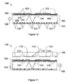
- FIG. 11 is a cross-sectional view of a second shutter-based spatial light modulator, according to the illustrative embodiment of the invention.
- FIGS. 12A-12D are cross-sectional views of third, fourth, fifth, and sixth illustrative shutter-based spatial light modulators, according to an embodiments of the invention.
- FIG. 13 is a cross-sectional view of a seventh shutter-based spatial light modulator, according to an illustrative embodiment of the invention.
- FIGS. 14A and 14B are cross-sectional views of two additional spatial light modulators, according to an illustrative embodiment of the invention.
- FIG. 15 is a cross-sectional view of an additional shutter assembly, according to an illustrative embodiment of the invention.
- FIG. 16 is a cross-sectional view of still a further spatial light modulator, according to an illustrative embodiment of the invention.
- FIG. 17 is an illustrative transflective shutter assembly, according to an embodiment of the invention.
- FIG. 18 is a second illustrative transflective shutter assembly, according to an embodiment of the invention.
- FIG. 19 is a cross-sectional view of a front reflective shutter assembly, according to an illustrative embodiment of the invention.
- FIG. 20 is an isometric view of a larger scale display formed from an array of light modulation arrays, according to an illustrative embodiment of the invention.
- FIG. 1A is an isometric conceptual view of an array 100 of light modulators (also referred to as a “light modulation array 100 ”), according to an illustrative embodiment of the invention.
- the light modulation array 100 includes a plurality of shutter assemblies 102 a - 102 d (generally “shutter assemblies 102 ”) arranged in rows and columns.
- a shutter assembly 102 has two states, open and closed (although partial openings can be employed to impart grey scale).
- Shutter assemblies 102 a and 102 d are in the open state, allowing light to pass.
- Shutter assemblies 102 b and 102 c are in the closed state, obstructing the passage of light.
- the light modulation array 100 can be utilized to form an image 104 for a projection or backlit display, illuminated by lamp 105 .
- each shutter assembly corresponds to a pixel 106 in the image 104 .
- a light modulation array includes three color-specific shutter assemblies for each pixel. By selectively opening one or more of the color-specific shutter assemblies corresponding to the pixel, the shutter assembly can generate a color pixel in the image.
- each shutter assembly 102 can be controlled using a passive matrix addressing scheme.
- Each shutter assembly 102 is controlled by a column electrode 108 and two row electrodes 110 a (a “row open electrode”) and 110 b (a “row close electrode”).
- all shutter assemblies 102 in a given column share a single column electrode 108 .
- All shutter assemblies in a row share a common row open electrode 110 a and a common row close electrode 110 b .
- An active matrix addressing scheme is also possible. Active matrix addressing (in which pixel and switching voltages are controlled by means of a thin film transistor array) is useful in situations in which the applied voltage must be maintained in a stable fashion throughout the period of a video frame.
- An implementation with active matrix addressing can be constructed with only one row electrode per pixel.
- the light modulation array 100 applies a potential to the column electrode 108 corresponding to the column of the light modulation array 100 in which the shutter assembly 102 is located and applies a second potential, in some cases having an opposite polarity, to the row open electrode 110 a corresponding to the row in the light modulation array 100 in which the shutter assembly 102 is located.
- the light modulation array 100 applies a potential to the column electrode 108 corresponding to the column of the light modulation array 100 in which the shutter assembly 102 is located and applies a second potential, in some cases having an opposite polarity, to the row close electrode 110 b corresponding to the row in the light modulation array 100 in which the shutter assembly 102 is located.
- a shutter assembly changes state in response to the difference in potential applied to the column electrode and one of the row electrodes 110 a or 110 b exceeding a predetermined switching threshold.
- light modulation array 100 sets the state of each shutter assembly 102 one row at a time in sequential order. For a given row, the light modulation array 100 first closes each shutter assembly 102 in the row by applying a potential to the corresponding row close electrode 110 b and a pulse of potential to all of the column electrodes 108 . Then, the light modulation array 100 opens the shutter assemblies 102 through which light is to pass by applying a potential to the row open electrode 110 a and applying a potential to the column electrodes 108 for the columns which include shutter assemblies in the row which are to be opened.
- the light modulation array 100 instead of closing each row of shutter assemblies 102 sequentially, after all rows in the light modulation array 100 are set to the proper position to form an image 104 , the light modulation array 100 globally resets all shutter assemblies 102 at the same time by applying a potentials to all row close electrodes 110 b and all column electrodes 108 concurrently. In another alternative mode of operation, the light modulation array 100 forgoes resetting the shutter assemblies 102 and only alters the states of shutter assemblies 102 that need to change state to display a subsequent image 104 .
- each shutter assembly includes a shutter 112 and an aperture 114 .
- the shutter To illuminate a pixel 106 in the image 104 , the shutter is positioned such that it allows light to pass, without any significant obstruction, through, the aperture 114 towards a viewer.
- the shutter 112 To keep a pixel unlit, the shutter 112 is positioned such that it obstructs the passage of light through the aperture 114 .
- the aperture 114 is defined by an area etched through a reflective material in each shutter assembly, such as the column electrode 108 .
- the aperture 114 may be filled with a dielectric material.
- FIG. 1B is a cross sectional diagram (see line A-A′ below in FIG. 1D ) of one of the shutter assemblies 102 of FIG. 1A , illustrating additional features of the shutter assemblies 102 .
- the shutter assembly 102 is built on a substrate 116 which is shared with other shutter assemblies 102 of the light modulation array 100 .
- the substrate 116 may support as many as 4,000,000 shutter assemblies, arranged in up to about 2000 rows and up to about 2000 columns.
- the shutter assembly 102 includes a column electrode 108 , a row open electrode 110 a , a row close electrode 110 b , a shutter 112 , and an aperture 114 .
- the column electrode 108 is formed from a substantially continuous layer of reflective metal, the column metal layer 118 , deposited on the substrate 116 .
- the column metal layer 118 serves as the column electrode 108 for a column of shutter assemblies 102 in the light modulation array 100 .
- the continuity of the column metal layer 118 is broken to electrically isolate one column electrode 108 from the column electrodes 108 of shutter assemblies 102 in other columns of the light modulation array 100 .
- each shutter assembly 102 includes an aperture 114 etched through the column metal layer 118 to form a light-transmissive region.
- the shutter assembly includes a row metal layer 120 , separated from the column metal layer 118 by one or more intervening layers of dielectric material or metal.
- the row metal layer 120 forms the two row electrodes 110 a and 110 b shared by a row of shutter assemblies 102 in light modulation array 100 .
- the row metal layer 120 also serves to reflect light passing through gaps in the column metal layer 118 other than over the apertures 114 .
- the column metal layer and the row metal layer are between about 0.1 and about 2 microns thick. In alternative implementations, such as depicted in FIG. 1D (described below), the row metal layer 120 can be located below the column metal layer 118 in the shutter assembly 102 .
- the shutter 102 assembly includes a third functional layer, referred to as the shutter layer 122 , which includes the shutter 112 .
- the shutter layer 122 can be formed from metal or a semiconductor.
- Metal or semiconductor vias 124 electrically connect the column metal layer 118 and the row electrodes 110 a and 110 b of the row metal layer 120 to features on the shutter layer 122 .
- the shutter layer 122 is separated from the row metal layer 120 by a lubricant, vacuum or air, providing the shutter 112 freedom of movement.
- FIG. 1C is a isometric view of a shutter layer 122 , according to an illustrative embodiment of the invention.
- the shutter layer 122 in addition to the shutter 112 , includes four shutter anchors 126 , two row anchors 128 a and 128 b , and two actuators 130 a and 130 b , each consisting of two opposing compliant beams.
- the shutter 112 includes an obstructing portion 132 and, optionally, as depicted in FIG. 1C , a shutter aperture 134 .
- a shutter assembly 102 can include additional apertures 114 and the shutter 112 can include multiple shutter apertures 134 .
- a shutter 112 can be designed with a series of narrow slotted shutter apertures 134 wherein the total area of the shutter apertures 134 is equivalent to the area of the single shutter aperture 134 depicted in FIG. 1C . In such implementations, the movement required of the shutter to move between open and closed states can be significantly reduced.
- Each actuator 130 a and 130 b is formed from two opposing compliant beams.
- a first pair of compliant beams, shutter actuator beams 135 physically and electrically connects each end of the shutter 112 to the shutter anchors 126 , located in each corner of the shutter assembly 102 .
- the shutter anchors 126 are electrically connected to the column metal layer 118 .
- the second pair of compliant beams, row actuator beams 136 a and 136 b extends from each row anchor 128 a and 128 b .
- the row anchor 128 a is electrically connected by a via to the row open electrode 110 a .
- the row anchor 128 b is electrically connected by a via to the row close electrode 110 b .
- the shutter actuator beams 135 and the row actuator beams 136 a and 136 b are formed from a deposited metal, such as Au, Cr or Ni, or a deposited semiconductor, such as polycrystalline silicon, or amorphous silicon, or from single crystal silicon if formed on top of a buried oxide (also known as silicon on insulator).
- the actuator beams 135 and 136 are patterned to dimensions of about 1 to about 20 microns in width, such that the actuator beams 135 and 136 are compliant.
- FIG. 1D is a top-view of the various functional layers of a light modulation array 100 ′, according to an illustrative embodiment of the invention.
- the light modulation array 100 ′ includes twelve shutter assemblies 102 ′ a - 102 ′ l , in various stages of completion.
- Shutter assemblies 102 ′ a and 102 ′ b include just the column metal layer 118 ′ of the light modulation array 100 ′.
- Shutter assemblies 102 ′ c - 102 ′ f include just the row metal layer 120 ′ (i.e., the row open electrode and the row-close electrode) of the light modulation array 100 ′.
- Shutter assemblies 102 ′ g and 102 ′ h include the column metal layer 118 ′ and the row metal layer 120 ′. In contrast to the shutter assembly 102 in FIG. 1B , the column metal layer 118 ′ is deposited on top of the row metal layer 120 ′. Shutter assemblies 102 ′ i - l depict all three functional layers of the shutter assemblies 102 ′, the row metal layer 120 ′, the column metal layer 118 ′, and a shutter metal layer 122 ′.
- the shutter assemblies 102 ′ i and 102 ′ k are closed, indicated by the column metal layer 118 ′ being visible through the shutter aperture 134 ′ included in the shutter assemblies 102 ′ i and 102 ′ k .
- the shutter assemblies 102 ′ j and 102 ′ l are in the open position, indicated by the aperture 114 ′ in the column metal layer 118 ′ being visible in the shutter aperture 134 ′.
- a shutter assembly can include multiple apertures and corresponding shutters and actuators (for example, between, 1 and 10) per pixel.
- the number of actuators activated can depend on the switching voltage that is applied or on the particular combination of row and column electrodes that are chosen for receipt of a switching voltage. Implementations are also possible in which partial openings of an aperture is made possible in an analog fashion by providing a switching voltages partway between a minimum and a maximum switching voltage. These alternative implementations provide an improved means of generating a grey scale.
- the shutter anchors 126 , the shutter 112 and the shutter actuator beams 135 become likewise energized with the applied potential.
- the corresponding row anchor 128 a or 128 b and the corresponding row actuator beam 136 a or 136 b also becomes energized.
- the row actuator beam 136 a or 136 b attracts its opposing shutter actuator beam 135 , thereby changing the state of the shutter assembly 102 .
- Each pair of actuator beams 135 and 136 i.e., a row actuator beam 134 a or 134 b and its opposing shutter actuator beam 135
- each pair is mechanically bi-stable.
- Each pair of actuator beams 135 and 136 is stable in two positions, one with the shutter 112 in an “open” position, and a second with the shutter 112 in a “closed” position.
- one stable position may have a lower energy state than the other stable position.
- the shutter assemblies 102 are designed such that the closed position has a lower energy state than the open position.
- a low energy reset pulse can therefore be applied to any or all pixels in order to return the entire array to its lowest stress state, corresponding also to an all-black image.
- the light modulation array 100 and its component shutter assemblies 102 are formed using standard micromachining techniques known in the art, including lithography; etching techniques, such as wet chemical, dry, and photoresist removal; thermal oxidation of silicon; electroplating and electroless plating; diffusion processes, such as boron, phosphorus, arsenic, and antimony diffusion; ion implantation; film deposition, such as evaporation (filament, electron beam, flash, and shadowing and step coverage), sputtering, chemical vapor deposition (CVD), epitaxy (vapor phase, liquid phase, and molecular beam), electroplating, screen printing, and lamination.
- lithography etching techniques, such as wet chemical, dry, and photoresist removal
- thermal oxidation of silicon such as boron, phosphorus, arsenic, and antimony diffusion
- ion implantation film deposition, such as evaporation (filament, electron beam, flash, and shadowing and step coverage), sputtering
- multiple layers of material are deposited on top of a substrate forming a stack.
- patterns are applied to a top most layer of the stack marking material either to be removed from, or to remain on, the stack.
- Various etching techniques including wet and/or dry etches, are then applied to the patterned stack to remove unwanted material.
- the etch process may remove material from one or more layers of the stack based on the chemistry of the etch, the layers in the stack, and the amount of time the etch is applied.
- the manufacturing process may include multiple iterations of layering, patterning, and etching.
- the process also includes a release step.
- sacrificial material is interdisposed in the stack proximate to material that will form moving parts in the completed device.
- An etch removes much of the sacrificial material, thereby freeing the parts to move.
- the surfaces of the moving shutter are insulated so that charge does not transfer between moving parts upon contact. This can be accomplished by thermal oxidation and/or by conformal chemical vapor deposition of an insulator such as Al2O3, Cr2O3, TiO2, HfO2, V2O5, Nb2O5, Ta2O5, SiO2, or Si3N4 or by depositing similar materials using techniques such as atomic layer deposition.
- the insulated surfaces are chemically passivated to prevent problems such as stiction between surfaces in contact by chemical conversion processes such as fluoridation or hydrogenation of the insulated surfaces.
- FIG. 2 is a cross-section of an optical cavity 200 for use in a spatial light modulator, according to an illustrative embodiment of the invention.
- the optical cavity 200 includes a front reflective surface 202 and a rear reflective surface 204 .
- the front reflective surface 202 includes an array of light-transmissive regions 206 through which light 208 can escape the optical cavity 200 .
- Light 208 enters the optical cavity 200 from one or more light sources 210 .
- the light 206 reflects between the front and rear reflective surfaces 202 and 204 until it reflects through one of the light-transmissive regions 206 . Additional reflective surfaces may be added along the sides of the optical cavity 200 .
- the front and rear reflective surfaces 202 and 204 are formed by depositing a metal or semiconductor onto either a glass or plastic substrate. In other implementations, the reflective surfaces 202 and 204 are formed by depositing metal or semiconductor on top of a dielectric film that is deposited as one of a series of thin films built-up on a substrate.
- the reflective surfaces 202 and 204 have reflectivities above about 50%. For example, the reflective surfaces 202 and 204 may have reflectivities of 70%, 85%, 96%, or higher.
- Smoother substrates and finer grained metals yield higher reflectivities.
- Smooth surfaces may be obtained by polishing a glass substrate or by molding plastic into smooth-walled forms. Alternatively, glass or plastic can be cast such that a smooth surface is formed by the settling of a liquid/air interface.
- Fine grained metal films without inclusions can be formed by a number of vapor deposition techniques including sputtering, evaporation, ion plating, laser ablation, or chemical vapor deposition.
- Metals that are effective for this reflective application include, without limitation, Al, Cr, Au, Ag, Cu, Ni, Ta, Ti, Nd, Nb, Si, Mo and/or alloys thereof.
- the reflective surface can be formed by interposing a dielectric material of low refractive index between a light guide in the optical cavity 200 and any of a series of thin films deposited on top of it.
- the change in refractive index between the light guide and the thin film leads to a condition of total internal reflection within the light guide, whereby incident light of sufficiently low incidence angle can be reflected with nearly 100% efficiency.
- the reflective surfaces 202 or 204 can be formed from a mirror, such as a dielectric mirror.
- a dielectric mirror is fabricated as a stack of dielectric thin films which alternate between materials of high and low refractive index. A portion of the incident light is reflected from each interface where the refractive index changes.
- Some dielectric mirrors have reflectivities greater than 99.8%.
- Dielectric mirrors can be custom-designed to accept a pre-specified range of wavelengths in the visible range and to accept a pre-specified range of incident angles. Reflectivities in excess of 99% under these conditions are possible as long as the fabricator is able to control the smoothness in the dielectric film stacks.
- the stacks can include between about 20 and about 500 films.
- first and second reflective surfaces 202 or 204 are included in the optical cavity 200 as separate components.
- a thin sheet of polished stainless steel or aluminum can suffice for this purpose.
- the light-transmissive regions 206 are arranged in an array to form pixels from which an image is formed.
- the light-transmissive regions 206 are spaced between about 100 and about 350 microns apart.
- the light transmissive regions are oblong or rectangular in shape, wherein the greater dimension is between about 50 and about 300 microns while the narrower dimension is between 2 and 100 microns, though other shapes and sizes may be suitable.
- the pitch can be as small as 20 microns, with aperture widths as small as 5 microns.
- the ratio between the area of the front reflective surface 202 taken up by light-transmissive regions 206 and the total area of the front reflective surface 202 is referred to herein as the transmissiveness ratio.
- Illustrative implementations of the optical cavity 200 have transmissiveness ratios of between about 5% and about 50%. Normally, spatial light modulators having such low transmissiveness ratios would emit insufficient light to form a usable image.
- the front and rear reflective surfaces 202 and 204 reflect the light 208 back and forth a number of times until the reflected light 208 passes through a light-transmissive region 206 , or until the light 208 loses its energy from the reflections. Higher reflectivity surfaces result in more light 208 escaping from the optical cavity 200 to form an image.
- one or more light sources 210 introduce light into the optical cavity 200 .
- the light source(s) 210 may be of any suitable type, including, for example, any of the types disclosed in U.S. Pat. Nos. 4,897,771 and 5,005,108, the entire disclosures of which are incorporated herein by reference.
- the light source(s) 210 may be an arc lamp, an incandescent bulb which also may be colored, filtered or painted, a lens end bulb, a line light, a halogen lamp, a light emitting diode (LED), a chip from an LED, a neon bulb, a fluorescent tube, a fiber optic light pipe transmitting from a remote source, a laser or laser diode, or any other suitable light source.
- the light sources may be a multiple colored LED, or a combination of multiple colored radiation sources 210 in order to provide a desired colored or white light output distribution.
- a plurality of colored lights such as LEDs of different colors (red, blue, green) or a single LED with multiple colored chips may be employed to create white light or any other colored light output distribution by varying the intensities of each individual colored light.
- a reflector may be positioned proximate to the light source 210 to reflect light 208 emitted away from the optical cavity 200 towards the optical cavity 200 .
- three light sources 210 , one red light source 210 , one green light source 210 , and one blue light source 210 sequentially introduce light 208 into the optical cavity 200 , alternating at frequencies in the range of 20 to 600 Hz. A rate in excess of 100 Hz is generally faster than what the human eye can detect, thus providing a color image.
- FIG. 3A is a linear cross-sectional view of a shutter assembly 300 in an open position.
- the shutter assembly 300 is formed on transparent substrate 302 having a thickness of from about 0.3 mm to about 2 mm.
- the substrate 302 can be, for example, made of a glass or a plastic.
- Suitable glasses include borosilicate glasses, or other glasses that can withstand processing temperatures up to or exceeding 400 degrees Centigrade.
- Suitable plastics for the substrate 302 include, for example, polyethyleneterephthalate (PET), or polytetrafluoroethylene (PETF), or other substantially transparent plastics that can withstand processing temperatures in excess of 200° C.
- Other candidate substrate materials include quartz and sapphire, which are understood to withstand processing temperatures in excess of 800° C.
- the lowest layer, referred to as the “column metal layer” 304 , of the shutter assembly 300 serves as the front reflective surface 202 of the optical cavity of FIG. 2 .
- an aperture 306 is etched through the column metal layer 304 to form a light-transmissive region, such as the light transmissive regions 206 of FIG. 2 .
- the aperture 306 can be generally circular, elliptical, polygonal, serpentine, or irregular in shape.
- the aperture occupies about 5% to about 25% of the area dedicated to the particular shutter assembly 300 in the light modulation array.
- the column metal layer 304 is substantially unbroken.
- the aperture 306 is filled with a dielectric material 307 .
- Example dielectrics suitable for inclusion in the shutter assembly 300 include SiO 2 , Si 3 N 4 , and Al 2 O 3 .
- the next layer is composed mostly of a dielectric material 307 , separating the column metal layer 304 from the row electrodes 308 a and 308 b disposed a layer above.
- the dielectric layers 316 may be between 0.3 and 10 microns thick.
- the top layer of the shutter assembly 300 includes a shutter anchor 312 , two row anchors 313 , two actuators, and a shutter 310 .
- the beams of the actuators are not shown as the cross section of the shutter assembly 300 is taken at a position in which the row actuator beams meet the row anchors 313 and the shutter actuator beams meet the shutter 310 (see, for example, line B-B′ on FIG. 1D ).
- the top layer is supported above the lower layers by the anchors 312 so that the shutter 310 is free to move.
- the row electrodes 308 a and 308 b are located at a lower layer in the shutter assembly 300 than the column metal layer 304 .
- the shutter 310 and actuators can be located at a layer below either of the column metal layer 304 or the row electrodes 308 a and 308 b.
- the actuators included in the shutter assembly may be designed to be mechanically bi-stable.
- the actuators can be designed to have only one stable position. That is, absent the application of some form of actuation force, such actuators return to a predetermined position, either open or closed.
- the shutter assembly 300 includes a single row electrode 308 , which, when energized, causes the actuator to push or pull the shutter 310 out of its stable position.
- FIG. 3B is a cross-sectional view of a second alternative shutter assembly 300 ′ in an open position according to an illustrative embodiment of the invention.
- the second shutter assembly 300 ′ includes a substrate 302 ′, a column metal layer 304 ′, an aperture 306 ′, row electrodes 308 a ′ and 308 b ′, a shutter 310 ′, two actuators, a shutter anchor 312 ′, and two row anchors 313 ′.
- the beams of the actuators are not shown as the cross section of the shutter assembly 300 ′ is taken at a position in which the row actuator beams meet the row anchors 313 ′ and the shutter actuator beams meet the shutter 310 ′. (See, for example, line B-B′ on FIG. 1D ).
- additional gaps are etched into the column metal layer 304 ′.
- the gaps electrically separate different portions of the column metal layer 304 ′ such that different voltages can be applied to each portion. For instance, in order to reduce parasitic capacitances that can arise between the column metal layer 304 ′ and the row electrodes 308 a ′ and 308 b ′ resulting from their overlap, a voltage can be selectively applied to the sections 314 of the column metal layer 304 ′ that immediately underlies the row electrodes 308 a ′ and 308 b ′ and the anchor 312 ′.
- FIG. 3C is a cross-sectional view of another third alternative shutter assembly 300 ′′ according to an illustrative embodiment of the invention.
- the shutter assembly 300 ′′ includes a substrate 302 ′′, a column metal layer 304 ′′, an aperture 306 ′′, row electrodes 308 a ′′ and 308 b ′′, a shutter 310 ′′, two actuators, a shutter anchor 312 ′′, and two row anchors 313 ′′.
- the beams of the actuators are not shown as the cross section of the shutter assembly 300 ′′ is taken at a position in which the row actuator beams meet the row anchors 313 ′′ and the shutter actuator beams meet the shutter 310 ′′. (See, for example, line B-B′ on FIG. 1D ).
- the shutter assembly 300 ′′ includes a reflective film 316 deposited on the substrate 302 ′′.
- the reflective film 316 serves as a front reflective surface for an optical cavity incorporating the shutter assembly 300 ′′. With the exception of an aperture 306 ′′ formed in the reflective film 316 to provide a light transmissive region, the reflective film 316 is substantially unbroken.
- a dielectric layer 318 separates the reflective film 316 from the column metal layer 304 ′′. At least one additional dielectric layer 318 separates the column metal layer 304 ′′ from the two row electrodes 308 a ′′ and 308 b ′′.
- the column metal layer 304 ′′ is etched to remove metal located below the row electrodes 308 a ′′ and 308 b ′′ to reduce potential capacitances that can form between the row electrodes 308 a ′′ and 308 b ′′ and the column metal layer 304 ′′. Gaps 320 formed in the column metal layer 304 ′′ are filled in with a dielectric.
- FIG. 3D is a cross-sectional view of a further alternative shutter assembly 300 ′′′ in a closed position according to an illustrative embodiment of the invention.
- the fourth alternative shutter assembly 300 ′′′ includes a substrate 302 ′′′, a column metal layer 304 ′′′, an aperture 306 ′′′, row electrodes 308 a ′′′ and 308 b ′′′, a shutter 310 ′′′, two actuators, a shutter anchors 312 ′′′, and two row anchors 313 ′′′.
- the beams of the actuators are not shown as the cross section of the shutter assembly 300 ′′′ is taken at a position in which the row actuator beams meet the row anchors 313 ′′′ and the shutter actuator beams meet the shutter 310 ′′′. (See, for example, line B-B′ on FIG. 1D ).
- much of the dielectric material used in building the fourth alternative shutter assembly 300 ′′′ is removed by one or more etching steps.
- the space previously occupied by the dielectric material can be filled with a lubricant to reduce friction and prevent stiction between the moving parts of the shutter assembly 300 ′′′.
- the lubricant fluid is engineered with viscosities preferably below about 10 centipoise and with relative dielectric constant preferably above about 2.0, and dielectric breakdown strengths above about 10 4 V/cm. Such mechanical and electrical properties are effective at reducing the voltage necessary for moving the shutter between open and closed positions.
- the lubricant preferably has a low refractive index, preferably less than about 1.5. In another implementation the lubricant has a refractive index that matches that of the substrate 302 .
- Suitable lubricants include, without limitation, de-ionized water, methanol, ethanol, silicone oils, fluorinated silicone oils, dimethylsiloxane, polydimethylsiloxane, hexamethyldisiloxane, and diethylbenzene.
- FIG. 4 is a cross sectional view of a shutter assembly 400 with a coated shutter 402 , according to an illustrative embodiment of the invention.
- the shutter assembly 400 is depicted as having the general structure of the shutter assembly 300 of FIG. 3A .
- the shutter assembly 400 can take the form of any of the shutter assemblies 102 , 300 , 300 ′, 300 ′′, or 300 ′′′ described above or any other shutter assembly described below.
- a reflective film 404 coats the bottom of the shutter 402 to reflect light 406 back through the shutter assembly 400 when the shutter 402 is in the closed position.
- Suitable reflective films 404 include, without limitation, smooth depositions of Al, Cr, or Ni. The deposition of such a film 404 , if the film 404 is greater than about 0.2 microns thick, provides a reflectivity for the shutter of 95% or higher.
- amorphous or polycrystalline Si when deposited onto a smooth dielectric surface, can provide reflectivity high enough to be useful in this application
- the top of the shutter 402 is coated with a light absorbing film 408 to reduce reflection of ambient light 410 striking the top of the shutter assembly 400 .
- the light absorbing film 408 can be formed from the deposition and/or anodization of a number of metals, such as Cr, Ni, or Au or Si in a manner that creates a rough or porous surface.
- the light absorbing film 408 can include an acrylic or vinyl resin which includes light absorbing pigments.
- the absorbing film 408 is applied to the entire, or substantially the entire top surface of the shutter assembly 400 .
- FIG. 5 is a cross sectional view of a shutter assembly 500 with a second coated shutter 502 , according to an illustrative embodiment of the invention.
- the shutter assembly 500 is depicted as having the general structure of the first alternative shutter assembly 300 of FIG. 3A .
- the shutter assembly can take the form of any of the shutter assemblies describes above 102 , 300 , 300 ′, 300 ′′, and 300 ′′′ or any other shutter assembly described below.
- both the top and the bottom of the shutter 502 are coated with a light absorbing film 504 such as a light absorbing film 408 .
- the light absorbing film 504 on the bottom of the shutter 502 absorbs light impacting the shutter 502 in a closed position.
- the intensity of light exiting the optical cavity is independent of the image being formed. That is, light intensity is independent of the fraction of shutters that may be in the open or the closed position.
- FIG. 6 is cross-sectional view of an elastically actuated shutter assembly 600 for use in a light modulation array, such as light modulation array 102 , according to an illustrative embodiment of the invention.
- the elastically actuated shutter assembly 600 includes a metal column layer 602 , a single row electrode 604 , an elastic element 606 , and a shutter 608 .
- the elastic element 606 provides a restoring force which keeps the shutter 608 in an open position, away from a corresponding aperture 610 in the column metal layer 602 . In the open position, light 612 can pass through the aperture 610 .
- the shutter assembly 600 may include a latch to lock the shutter 608 into a closed position such that after the shutter 608 closes, the row electrode 604 can be de-energized without the shutter 608 opening. To open the shutter 608 , the latch is released.
- the elastic actuator tends to keep the shutter 608 in a closed position. Applying a voltage to the row electrode 604 moves the shutter 608 into an open position. Suitable spring-like elastic actuators for displays have been described in U.S. Pat. No. 5,062,689, the entirety of which is incorporated herein by reference.
- FIG. 7 is a cross-sectional view of a shutter assembly 700 with a deformable shutter 701 for use in a light modulation array, according to an illustrative embodiment of the invention.
- the shutter assembly 700 includes a column metal layer 702 , and one row electrode 704 formed on a substrate 708 .
- the deforming shutter 701 instead of translating from one side of the shutter assembly 700 to the other side of the shutter assembly 700 to open and close, deforms in response to the energizing of the row electrode 704 .
- the deforming shutter 701 is formed such that the deforming shutter 701 retains residual stress, resulting in the deforming shutter 701 tending to curl up out of the plane of the light modulation array in which it is included.
- the deforming shutter 701 is attracted towards the substrate 708 , thereby covering an aperture 710 formed in the column metal layer 702 .
- Deformable or hinge type actuators have been described in the art, for instance in U.S. Pat. Nos. 4,564,836 and 6,731,492, the entireties of which are incorporated herein by reference.
- FIG. 8A is a cross-sectional view of a shutter assembly 800 with an opaque substrate 802 , such as silicon, for use in a light modulation array, according to an illustrative embodiment of the invention.
- the opaque substrate 802 has a thickness in the range of about 200 microns to about 1 mm.
- the shutter assembly 800 resembles the shutter assembly 300 of FIG. 3A
- the shutter assembly 800 can take substantially the same form of any of the shutter assemblies 300 , 300 ′, 300 ′′, 300 ′′′, 400 , 500 , 600 , or 700 described in FIGS. 3-7 .
- An aperture 804 is etched through the entirety of the opaque substrate 802 .
- the aperture 804 is formed using an anisotropic dry etch such as in a CFCl 3 gas with plasma or ion assist.
- the shutter assembly 800 may also include a reflective coating 810 deposited on the side of the opaque substrate 802 opposite the column metal layer.
- FIG. 8B is a cross-sectional view of a second shutter assembly 800 ′ with an opaque substrate 802 ′ for use in a light modulation array, according to an illustrative embodiment of the invention.
- the underside of the opaque substrate 800 ′ is etched away forming cavities 806 beneath the apertures 804 ′ of the shutter assembly 800 ′.
- the cavities 806 allow light from a larger range of angles to escape through the aperture 804 ′. The larger range provides for a brighter image and a larger viewing angle.
- shutter assemblies described in FIGS. 1 and 3 - 8 depend on electrostatic forces for actuation.
- a number of alternative actuator forcing mechanisms can be designed into shutter assemblies, including without limitation the use of electromagnetic actuators, thermoelastic actuators, piezoelectric actuators, and electrostiction actuators.
- Other shutter motions which can be used to controllably obstruct an aperture include without limitation sliding, rotating, bending, pivoting, hinging, or flapping; all motions which are either within the plane of the reflective surface or transverse to that plane.
- FIG. 9 is a cross-sectional view of a liquid crystal-based spatial light modulator 900 .
- the liquid crystal-based spatial light modulator 900 includes an array 901 of liquid crystal cells 902 .
- the liquid crystal cells 902 include pairs of opposing transparent electrodes 904 on either side of a layer of liquid crystal molecules 906 .
- the liquid crystal-based spatial light modulator 900 includes a polarizer 908 .
- the liquid crystal-based spatial light modulator 900 includes an analyzer 910 . Thus, without intervention, light passing through the polarizer 908 would be filtered blocked by the analyzer 910 .
- the liquid crystal molecules 906 between the electrodes 904 align themselves with the resultant electric field reorienting the light passing through the polarizer 908 such that it can pass through the analyzer 910 .
- the polarizer 908 is positioned on top of a front reflective surface 911 , which defines a plurality of light-transmission regions 913 .
- the array 901 is attached to an optical cavity, such as optical cavity 200 and includes a cover plate 912 . Cover plates are described in further detail in relation to FIG. 11 .
- Each liquid crystal cell 902 may have a corresponding red, green, or blue color specific filter.
- color differentiation can be provided by multiple lamps operating in sequence as described above in relation to FIG. 2 .
- liquid crystal displays are designed with resolutions of 80 to 110 dots per inch, wherein pixel widths are in the range of 250 to 330 microns.
- the transmissiveness ratio of the liquid-crystal display is in the range of 75 to 90%.
- the overhead required for TFT addressing can limit the available transmissiveness ratio to about 30 or 50%.
- Such high-resolution displays therefore, typically suffer from a lower luminous efficiency than their lower-resolution counterparts due to a loss of aperture ratio.
- FIG. 10 is a cross sectional view of a first shutter-based spatial light modulator 1000 according to an illustrative embodiment of the invention.
- the shutter-based spatial light modulator 1000 includes a light modulation array 1002 , an optical cavity 1004 , and a light source 1006 .
- the light modulation array 1002 can include any of the shutter assemblies 300 , 300 ′, 300 ′′, 300 ′′′, 400 , 500 , 600 , 700 , 800 , or 800 ′ described above in FIGS. 3-8 .
- the optical cavity 1004 in the first shutter-based spatial light modulator 1000 , is formed from a light guide 1008 having front and rear surfaces.
- a front reflective surface 1010 is deposited directly on the front surface of the light guide 1008 and a second reflective surface 1012 is deposited directly on the rear surface of the light guide 1008 .
- the light guide 1008 can be formed from glass or a transparent plastic such as polycarbonate or polyethylene.
- the light guide 1008 is about 300 microns to about 2 mm thick.
- the light guide 1008 distributes light 1014 introduced into the optical cavity 1004 substantially uniformly across the surface of the front reflective surface 1010 .
- the light guide 1008 achieves such distribution by means of a set of total internal reflections as well as by the judicial placement of light scattering elements 1016 .
- the light scattering elements 1016 can be formed in or on the rear side of the light guide 1018 to aid in redirecting light 1014 out of the light guide 1008 and through light-transmissive regions 1019 formed in the front reflective surface 1010 .
- FIG. 11 is a cross sectional view of a second shutter-based spatial light modulator 1100 , according to the illustrative embodiment of the invention.
- the second shutter-based spatial light modulator 1100 includes a light modulation array 1102 , an optical cavity 1104 , and a light source 1106 .
- the second spatial light modulator includes a cover plate 1108 .
- the cover plate 1108 serves several functions, including protecting the light modulation array 1102 from mechanical and environmental damage.
- the cover plate 1108 is a thin transparent plastic, such as polycarbonate, or a glass sheet.
- the cover plate can be coated and patterned with a light absorbing material, also referred to as a black matrix 1110 .
- the black matrix can be deposited onto the cover plate as a thick film acrylic or vinyl resin that contains light absorbing pigments.
- the black matrix 1110 absorbs substantially all incident ambient light 1112 —ambient light is light that originates from outside the spatial light modulator 1100 , from the vicinity of the viewer—except in patterned light-transmissive regions 1114 positioned substantially proximate to light-transmissive regions 1116 formed in the optical cavity 1104 .
- the black matrix 1110 thereby increases the contrast of an image formed by the spatial light modulator 1100 .
- the black matrix 1110 can also function to absorb light escaping the optical cavity 1104 that may be emitted, in a leaky or time-continuous fashion.
- color filters for example, in the form of acrylic or vinyl resins are deposited on the cover plate 1108 .
- the filters may be deposited in a fashion similar to that used to form the black matrix 1110 , but instead, the filters are patterned over the open apertures light transmissive regions 1116 of the optical cavity 1104 .
- the resins can be doped alternately with red, green, or blue pigments.
- the spacing between the light modulation array 1102 and the cover plate 1108 is less than 100 microns, and may be as little as 10 microns or less.
- the light modulation array 1102 and the cover plate 1108 preferably do not touch, except, in some cases, at predetermined points, as this may interfere with the operation of the light modulation array 1102 .
- the spacing can be maintained by means of lithographically defined spacers or posts, 2 to 20 microns tall, which are placed in between the individual right modulators in the light modulators array 102 , or the spacing can be maintained by a sheet metal spacer inserted around the edges of the combined device.
- FIG. 12A is a cross sectional view of a third shutter-based spatial light modulator 1200 , according to an illustrative embodiment of the invention.
- the third shutter-based spatial light modulator 1200 includes an optical cavity 1202 , a light source 1204 , and a light modulation array 1206 .
- the third shutter-based spatial light modulator 1204 includes a cover plate 1207 , such as the cover plate 1108 described in relation to FIG. 11 .
- the optical cavity 1202 in the third shutter-based spatial light modulator 1200 , includes a light guide 1208 and the rear-facing portion of the light modulation array 1206 .
- the light modulation array 1206 is formed on its own substrate 1210 . Both the light guide 1208 and the substrate 1210 each have front and rear sides.
- the light modulation array 1206 is formed on the front side of the substrate 1210 .
- a front-facing, rear-reflective surface 1212 in the form of a second metal layer, is deposited on the rear side of the light guide 1208 to form the second reflective surface of the optical cavity 1202 .
- the optical cavity 1202 includes a third surface located behind and substantially facing the rear side of the light guide 1208 .
- the front-facing, rear-reflective surface 1212 is deposited on the third surface facing the front of the spatial light modulator 1200 , instead of directly on the rear side of the light guide 1208 .
- the light guide 1208 includes a plurality of light scattering elements 1209 , such as the light scattering elements 1016 described in relation to FIG. 10 . As in FIG. 10 , the light scattering elements are distributed in a predetermined pattern on the rear-facing side of the light guide 1208 to create a more uniform distribution of light throughout the optical cavity.
- the light guide 1208 and the substrate 1210 are held in intimate contact with one another. They are preferably formed of materials having similar refractive indices so that reflections are avoided at their interface. In another implementation small standoffs or spacer materials keep the light guide 1208 and the substrate 1210 a predetermined distance apart, thereby optically de-coupling the light guide 1208 and substrate 1210 from each other. The spacing apart of the light guide 1208 and the substrate 1210 results in an air gap 1213 forming between the light guide 1208 and the substrate 1210 .
- the air gap promotes total internal reflections within the light guide 1208 at its front-facing surface, thereby facilitating the distribution of light 1214 within the light guide before one of the light scattering elements 1209 causes the light 1214 to be directed toward the light modulator array 1206 shutter assembly.
- the gap between the light guide 1208 and the substrate 1210 can be filled by a vacuum, one or more selected gasses, or a liquid.
- FIG. 12B is a cross sectional view of a fourth shutter-based spatial light modulator 1200 ′, according to an illustrative embodiment of the invention.
- the fourth spatial light modulator 1200 ′ includes an optical cavity 1202 ′, a light source 1204 ′, a light modulation array 1206 ′, and a cover plate 1207 ′, such as the cover plate 1108 described in relation to FIG. 11 .
- the optical cavity 1202 ′ includes a rear-facing reflective surface in the light modulation array 1206 ′, a light guide 1208 ′, and a front-facing rear-reflective surface 1212 ′.
- the light modulation array 1206 ′ of the fourth spatial light modulator 1200 ′ is formed on a substrate 1210 ′, which is separate from the light guide 1208 ′.
- the light guide 1208 ′ and the substrate 1210 ′ are separated by a light diffuser 1218 and a brightness enhancing film 1220 .
- the diffuser 1218 helps to randomize the optical angles of scattered light 1214 ′ to improve uniformity and reduce the formation of ghost images from the light source 1204 or the light modulation array 1206 .
- the brightness enhancement film 1220 includes an array of optical prisms that are molded into a thin plastic sheet, and which act to funnel light into a narrow cone of illumination.
- the brightness enhancing film 1220 re-directs light leaving the light guide 1208 ′ through light-transmissive regions 1222 at an oblique angle towards the viewer, thus resulting in an apparent increases in brightness along the optical axis for the same input power.
- FIG. 12C is a cross sectional view of a fifth shutter-based spatial light modulator 1200 ′′, according to an illustrative embodiment of the invention.
- the fifth spatial light modulator 1200 ′′ includes an optical cavity 1202 ′′, a light source 1204 ′′, a light modulation array 1206 ′′, and a cover plate 1207 ′′, such as the cover plate 1108 described in relation to FIG. 11 .
- the optical cavity 1202 ′′ includes a rear-facing reflective surface in the light modulation array 1206 ′′, a light guide 1208 ′′, and a front-facing rear-reflective surface 1212 ′′.
- the light modulation array 1206 ′′ of the fifth spatial light modulator 1200 ′′ is formed on a substrate 1210 ′′, which is separate from the light guide 1208 ′′.
- the light guide 1208 ′′ and the substrate 1210 ′′ are separated by a microlens array 1224 .
- the microlens array 1224 re-directs light 1214 ′′ leaving the light guide 1208 ′′ through light-transmissive regions 1222 ′ at an oblique angle towards the viewer, thus resulting in an apparent increases in brightness for the same input power.
- the light guide 1208 ′′ can be constructed of a moldable plastic, without the transition temperature of the plastic limiting the manufacturing processes available for constructing the light modulation array 1210 ′′.
- the light guide 1208 ′′ can be molded to substantially encapsulate the light source 1204 ′′ used to introduce light 1214 ′′ into the optical cavity 1202 ′′.
- the encapsulation of the light source 1204 ′′ into the light guide 1208 ′′ provides improved coupling of light 1214 ′′ into the light guide 1208 ′′.
- scattering elements 1209 ′′ can be incorporated directly in the mold for the light guide 1208 ′′.
- FIG. 12D is a cross-sectional view of a sixth illustrative embodiment of a shutter-based light modulation array 1200 ′′′.
- the sixth spatial light modulator 1200 ′′′ includes an optical cavity 1202 ′′′, a light source 1204 ′′′, a light modulation array 1206 ′′′, and a cover plate 1207 ′′′, such as the cover plate 1108 described in relation to FIG. 11 .
- the optical cavity 1202 ′′′ includes a rear-facing reflective surface in the light modulation array 1206 ′′′, a light guide 1208 ′′′, a front-facing rear-reflective surface 1212 ′′′, a diffuser 1218 ′′′, and a brightness enhancing film 1220 ′′′.
- the space between the light modulation array 1206 ′′′ and the cover plate 1207 ′′′ is filled with a lubricant 1224 , such as the lubricant described in relation to FIG. 3D .
- the cover plate 1207 ′′′ is attached to the shutter assembly 1206 with an epoxy 1225 .
- the epoxy should have a curing temperature preferably below about 20° C., it should have a coefficient of thermal expansion preferably below about 50 ppm per degree C. and should be moisture resistant.
- An exemplary epoxy is EPO-TEK B9021-1, sold by Epoxy Technology, Inc. The epoxy also serves to seal in the lubricant 1224 .
- a sheet metal or molded plastic assembly bracket 1226 holds the cover plate 1207 ′′′, the light modulation array 1206 ′′′, and the optical cavity 1202 ′′′ together around the edges.
- the assembly bracket 1226 is fastened with screws or indent tabs to add rigidity to the combined device.
- the light source 1204 ′′′ is molded in place by an epoxy potting compound.
- FIG. 13 is a cross-sectional view of a seventh shutter-based spatial light modulator 1300 according to an illustrative embodiment of the invention.
- the seventh shutter-based spatial light modulator 1300 includes a substrate 1302 on which a light modulation array 1304 is formed, and a light guide 1306 .
- the light modulation array 1304 includes a front reflective surface for the optical cavity 1310 of the spatial light modulator 1300 .
- a reflective material is deposited or adhered to the rear side of the light guide to serve as a rear reflective surface 1308 .
- the rear side of the light guide 1306 is angled or shaped with respect to the front side of the light guide 1308 to promote uniform distribution of light in the light modulation array 1304 .
- the rear reflective surface 1308 is still partially facing the front reflective surface.
- FIG. 14A is a cross-sectional view of another spatial light modulator 1400 , according to an illustrative embodiment of the invention.
- the spatial light modulator 1400 includes a substrate 1402 on which a light modulation array 1404 is formed.
- the light modulation array includes a reflective surface serving as a front reflective surface 1405 of an optical cavity.
- the spatial light modulation 1400 also includes a rear reflective surface 1406 substantially facing the rear side of the light modulation array 1404 .
- a light source 1408 is positioned within the space formed between the substrate 1402 on which the light modulation array 1404 is formed and the rear reflective surface 1406 .
- the space may also be filled with a substantially transparent plastic into which the light source 1408 is embedded.
- FIG. 14B is a cross-sectional view of another spatial light modulator 1400 ′, similar to the spatial light modulator 1400 of FIG. 14A .
- the spatial light modulator 1400 ′ includes a substrate 1402 ′ on which a light modulation array 1404 ′ is formed.
- the light modulation array 1404 ′ includes a reflective surface serving as a front reflective surface 1405 of an optical cavity.
- the spatial light modulation 1400 ′ also includes a rear reflective surface 1406 ′.
- the rear reflective surface 1406 ′ is corrugated, textured, or shaped to promote light distribution in the optical cavity formed by the reflective surfaces (i.e., the rear reflective surface 1406 ′ and a reflective surface incorporated into the light modulation array 1404 ′ of the spatial light modulator 1400 ′.
- FIG. 15 is a cross-sectional view of another shutter assembly 1500 for use in a light modulation array, according to an illustrative embodiment of the invention.
- the shutter assembly 1500 includes a metal column layer 1502 , two row electrodes 1504 a and 1504 b , a shutter 1506 , built on a substrate 1509 .
- the shutter assembly 1500 also includes one or more light scattering elements 1508 .
- an aperture 1510 is etched through the column metal layer 1502 .
- the light scattering elements 1510 can include any change in the shape or geometry of the substrate 1509 , such as by roughening, coating, or treating the surface of the substrate 1509 .
- the light scattering elements can include patterned remnants of the column metal 1502 having dimensions of about 1 to about 5 microns.
- the light scattering elements 1508 aid in extracting light 1512 trapped in the substrate 1508 due to total internal reflection. When such trapped light 1512 strikes one of the scattering elements 1508 , the angle of the light's 1512 path changes. If the angle of the light's 1512 path becomes sufficiently acute, it passes out of the substrate 1509 . If the shutter 1506 is in the open position, the scattered light 1512 can exit the aperture 1510 , and proceed to a viewer as part of an image.
- FIG. 16 is a cross sectional view of yet another spatial light modulator 1600 according to an illustrative embodiment of the invention.
- the spatial light modulator 1600 includes a light modulation array 1602 formed on the rear surface of a substrate 1604 , facing the interior of an optical cavity 1606 .
- the individual light modulation elements 1608 such as the shutter assemblies 300 , 300 ′, 300 ′′, 300 ′′′, 400 , 500 , 600 , 700 , 800 , and 800 ′ described in FIGS. 3-8 or the liquid-crystal cells 902 described in FIG. 9 , making up the light modulation array 1602 are modified to reverse the sides of the light modulation elements 1608 that reflect or absorb light as compared to what is described with reference to FIGS. 4 and 5 .
- the optical cavity 1606 includes both a front reflective surface 1610 , a rear reflective surface 1612 , and a light guide 1614 .
- Light is introduced into the optical cavity by a light source 1613 .
- the front reflective surface 1610 is disposed on front-facing surface of the light guide 1614 , providing a substantially continuous layer of high reflectivity and also defining light transmissive region 1616 .
- the front reflective surface 1610 is separated from the light modulation array 1602 by a transparent gap 1618 .
- the gap 1618 is preferably narrower than width of the light transmissive regions 1616 , less than, for example, about 100 microns.
- the gap 1618 may be as narrow as about 10 microns wide, or even narrower.
- the gap 1618 is filled with a lubricant 1620 , such as the lubricant described in relation to FIG. 3D .
- the lubricant 1620 may have a refractive index that substantially matches that of the light guide 1614 to facilitate the extraction of light from the light guide 1614 .
- the spatial light modulator 1600 can optionally forego a cover plate, since the shutter assembly is protected by the environment by the substrate 1604 . If a cover plate is omitted, a black matrix, such as the black matrix 1110 of FIG. 11 , can be applied to the front-facing surface of the substrate 1604 .
- FIG. 17 is a cross-sectional view of a transflective shutter assembly 1700 , according to an illustrative embodiment of the invention, which can be incorporated into the spatial light modulators 1000 , 1100 , 1200 , 1300 , 1400 , and 1500 described in FIGS. 10-15 .
- the transflective shutter assembly 1700 forms images from both light 1701 emitted by a light source positioned behind the shutter assembly 1700 and from ambient light 1703 .
- the transflective shutter assembly 1700 includes a metal column layer 1702 , two row electrodes 1704 a and 1704 b , and a shutter 1706 .
- the transflective shutter assembly 1700 includes an aperture 1708 etched through the column metal layer 1702 . Portions of the column metal layer 1702 , having dimensions of from about 1 to about 5 microns, are left on the surface of the aperture 1708 to serve as transflection elements 1710 .
- a light absorbing film 1712 covers the top surface of the shutter 1706 .
- the transflective shutter assembly 1700 While the shutter is in the closed position, the light absorbing film 1712 absorbs ambient light 1703 impinging on the top surface of the shutter 1706 . While the shutter 1706 is in the open position as depicted in FIG. 17 , the transflective shutter assembly 1700 contributes to the formation of an image both by allowing light 1701 to pass through the transflective shutter assembly originating from the dedicated light source and from reflected ambient light 1703 . The small size of the transflective elements 1710 results in a somewhat random pattern of ambient light 1703 reflection.
- the transflective shutter assembly 1700 is covered with a cover plate 1714 , which includes a black matrix 1716 .
- the black matrix absorbs light, thereby substantially preventing ambient light 1703 from reflecting back to a viewer unless the ambient light 1703 reflects off of an uncovered aperture 1708 .
- FIG. 18 is a cross-sectional view of a second transflective shutter assembly 1800 according to an illustrative embodiment of the invention, which can be incorporated into the spatial light modulators 1000 , 1100 , 1200 , 1300 , 1400 , and 1500 described in FIGS. 10-15 .
- the transflective shutter assembly 1800 includes a metal column layer 1802 , two row electrodes 1804 a and 1804 b , and a shutter 1806 .
- the transflective shutter assembly 1800 includes an aperture 1808 etched through the column metal layer 1702 . At least one portion of the column metal layer 1802 , having dimensions of from about 5 to about 20 microns, remains on the surface of the aperture 1808 to serve as a transflection element 1810 .
- a light absorbing film 1812 covers the top surface of the shutter 1806 . While the shutter is in the closed position, the light absorbing film 1812 absorbs ambient light 1803 impinging on the top surface of the shutter 1806 . While the shutter 1806 is in the open position, the transflective element 1810 reflects a portion of ambient light 1803 striking the aperture 1808 back towards a viewer. The larger dimensions of the transflective element 1810 in comparison to the transflective elements 1710 yield a more specular mode of reflection, such that ambient light originating from behind the viewer is substantially reflected directly back to the viewer.
- the transflective shutter assembly 1800 is covered with a cover plate 1814 , which includes a black matrix 1816 .
- the black matrix absorbs light, thereby substantially preventing ambient light 1803 from reflecting back to a viewer unless the ambient light 1803 reflects off of an uncovered aperture 1808 .
- the transflective shutter assemblies 1700 and 1800 are incorporated into spatial light modulators having optical cavities and light sources, as described above, the ambient light 1703 and 1803 passing through the apertures 1708 and 1808 enters the optical cavity and is recycled along with the light introduced by the light source.
- the apertures in the column metal are at least partially filled with a semi-reflective-semitransmissive material.
- FIG. 19 is a cross sectional view of a front reflective shutter assembly 1900 according to an illustrative embodiment of the invention.
- the front reflective shutter assembly 1900 can be used in a reflective light modulation array.
- the front reflective shutter assembly 1900 reflects ambient light 1902 towards a viewer.
- use of arrays of the front reflective shutter assembly 1900 in spatial light modulators obviates the need for a dedicated light source in viewing environments having high amounts of ambient light 1902 .
- the front reflective shutter assembly 1900 can take substantially the same form of the shutter assemblies 300 , 300 ′, 300 ′′, 300 ′′′, 400 , 500 , 600 , 700 , 800 or 800 ′ of FIGS. 3-8 .
- the column metal layer includes a reflective surface beneath the position of a closed shutter 1904 .
- the front-most layer of the reflective shutter assembly 1900 including at least the front surface of the shutter 1904 , is coated in a light absorbing film 1908 .
- light 1902 impinging on the reflective shutter assembly 1900 is absorbed.
- the shutter 1904 is open, at least a fraction of the light 1902 impinging on the reflective shutter assembly 1900 reflects off the exposed column metal layer 1910 back towards a viewer.
- the column metal layer 1910 can be covered with an absorbing film while the front surface of shutter 1908 can be covered in a reflective film. In this fashion light is reflected back to the viewer only when the shutter is closed.
- the reflective shutter assembly 1900 can be covered with a cover plate 1910 having a black matrix 1912 applied thereto.
- the black matrix 1912 covers portions of the cover plate 1910 not opposing the open position of the shutter.
- FIG. 20 is an isometric view of a spatial light modulator 2000 including multiple light modulation arrays 2002 , according to an illustrative embodiment of the invention.
- the size of several of the light modulation arrays 2002 described above is limited, somewhat, by the semiconductor manufacturing techniques used to construct them.
- light guides 2004 and reflective films 2006 can be formed on a significantly larger scale.
- a spatial light modulator which includes multiple, adjacently disposed light modulation arrays 2002 , arranged over one or more light guides 2004 , can generate a larger image, thereby circumventing these limitations.
Abstract
Description
| TABLE 1 | ||
| Transmissiveness | ||
| Ratio | Reflectivity | Efficiency |
| 8% | 0.97 | 59% |
| 0.93 | 40% | |
| 0.88 | 30% | |
| 14% | 0.97 | 71% |
| 0.93 | 55% | |
| 0.88 | 43% | |
| 20% | 0.97 | 79% |
| 0.93 | 65% | |
| 0.88 | 53% | |
Claims (12)
Priority Applications (1)
| Application Number | Priority Date | Filing Date | Title |
|---|---|---|---|
| US11/973,002 US7927654B2 (en) | 2005-02-23 | 2007-10-04 | Methods and apparatus for spatial light modulation |
Applications Claiming Priority (4)
| Application Number | Priority Date | Filing Date | Title |
|---|---|---|---|
| US65582705P | 2005-02-23 | 2005-02-23 | |
| US67605305P | 2005-04-29 | 2005-04-29 | |
| US11/218,690 US7417782B2 (en) | 2005-02-23 | 2005-09-02 | Methods and apparatus for spatial light modulation |
| US11/973,002 US7927654B2 (en) | 2005-02-23 | 2007-10-04 | Methods and apparatus for spatial light modulation |
Related Parent Applications (1)
| Application Number | Title | Priority Date | Filing Date |
|---|---|---|---|
| US11/218,690 Continuation US7417782B2 (en) | 2003-02-23 | 2005-09-02 | Methods and apparatus for spatial light modulation |
Publications (2)
| Publication Number | Publication Date |
|---|---|
| US20080145527A1 US20080145527A1 (en) | 2008-06-19 |
| US7927654B2 true US7927654B2 (en) | 2011-04-19 |
Family
ID=36539269
Family Applications (8)
| Application Number | Title | Priority Date | Filing Date |
|---|---|---|---|
| US11/218,690 Active US7417782B2 (en) | 2003-02-23 | 2005-09-02 | Methods and apparatus for spatial light modulation |
| US11/546,937 Active US7391552B2 (en) | 2005-02-23 | 2006-10-11 | Methods and apparatus for spatial light modulation |
| US11/594,042 Active US7619806B2 (en) | 2005-02-23 | 2006-11-06 | Methods and apparatus for spatial light modulation |
| US11/712,630 Active US7365897B2 (en) | 2005-02-23 | 2007-02-28 | Methods and apparatus for spatial light modulation |
| US11/973,002 Expired - Fee Related US7927654B2 (en) | 2005-02-23 | 2007-10-04 | Methods and apparatus for spatial light modulation |
| US11/981,168 Active US7742215B2 (en) | 2005-02-23 | 2007-10-30 | Methods and apparatus for spatial light modulation |
| US12/030,146 Active US7460290B2 (en) | 2005-02-23 | 2008-02-12 | Methods and apparatus for spatial light modulation |
| US12/049,852 Active US7729037B2 (en) | 2005-02-23 | 2008-03-17 | Methods and apparatus for spatial light modulation |
Family Applications Before (4)
| Application Number | Title | Priority Date | Filing Date |
|---|---|---|---|
| US11/218,690 Active US7417782B2 (en) | 2003-02-23 | 2005-09-02 | Methods and apparatus for spatial light modulation |
| US11/546,937 Active US7391552B2 (en) | 2005-02-23 | 2006-10-11 | Methods and apparatus for spatial light modulation |
| US11/594,042 Active US7619806B2 (en) | 2005-02-23 | 2006-11-06 | Methods and apparatus for spatial light modulation |
| US11/712,630 Active US7365897B2 (en) | 2005-02-23 | 2007-02-28 | Methods and apparatus for spatial light modulation |
Family Applications After (3)
| Application Number | Title | Priority Date | Filing Date |
|---|---|---|---|
| US11/981,168 Active US7742215B2 (en) | 2005-02-23 | 2007-10-30 | Methods and apparatus for spatial light modulation |
| US12/030,146 Active US7460290B2 (en) | 2005-02-23 | 2008-02-12 | Methods and apparatus for spatial light modulation |
| US12/049,852 Active US7729037B2 (en) | 2005-02-23 | 2008-03-17 | Methods and apparatus for spatial light modulation |
Country Status (9)
| Country | Link |
|---|---|
| US (8) | US7417782B2 (en) |
| EP (1) | EP1855986B1 (en) |
| JP (9) | JP5748387B2 (en) |
| KR (11) | KR101458477B1 (en) |
| CN (4) | CN102401992B (en) |
| AT (1) | ATE513785T1 (en) |
| BR (1) | BRPI0607881A2 (en) |
| CA (7) | CA2803823A1 (en) |
| WO (1) | WO2006091904A2 (en) |
Cited By (33)
| Publication number | Priority date | Publication date | Assignee | Title |
|---|---|---|---|---|
| US20080192065A1 (en) * | 2005-08-02 | 2008-08-14 | Uni-Pixel Displays, Inc. | Mechanism to Mitigate Color Breakup Artifacts in Field Sequential Color Display Systems |
| US8482496B2 (en) | 2006-01-06 | 2013-07-09 | Pixtronix, Inc. | Circuits for controlling MEMS display apparatus on a transparent substrate |
| US8519945B2 (en) | 2006-01-06 | 2013-08-27 | Pixtronix, Inc. | Circuits for controlling display apparatus |
| US8519923B2 (en) | 2005-02-23 | 2013-08-27 | Pixtronix, Inc. | Display methods and apparatus |
| US8780540B2 (en) | 2012-03-02 | 2014-07-15 | Microsoft Corporation | Flexible hinge and removable attachment |
| US8786767B2 (en) | 2012-11-02 | 2014-07-22 | Microsoft Corporation | Rapid synchronized lighting and shuttering |
| US20140253539A1 (en) * | 2013-03-07 | 2014-09-11 | International Business Machines Corporation | Systems and methods for displaying images |
| US8850241B2 (en) | 2012-03-02 | 2014-09-30 | Microsoft Corporation | Multi-stage power adapter configured to provide low power upon initial connection of the power adapter to the host device and high power thereafter upon notification from the host device to the power adapter |
| US8873227B2 (en) | 2012-03-02 | 2014-10-28 | Microsoft Corporation | Flexible hinge support layer |
| US9075566B2 (en) | 2012-03-02 | 2015-07-07 | Microsoft Technoogy Licensing, LLC | Flexible hinge spine |
| US9082353B2 (en) | 2010-01-05 | 2015-07-14 | Pixtronix, Inc. | Circuits for controlling display apparatus |
| US9087486B2 (en) | 2005-02-23 | 2015-07-21 | Pixtronix, Inc. | Circuits for controlling display apparatus |
| US9116344B2 (en) | 2008-10-27 | 2015-08-25 | Pixtronix, Inc. | MEMS anchors |
| US9128277B2 (en) | 2006-02-23 | 2015-09-08 | Pixtronix, Inc. | Mechanical light modulators with stressed beams |
| US9134552B2 (en) | 2013-03-13 | 2015-09-15 | Pixtronix, Inc. | Display apparatus with narrow gap electrostatic actuators |
| US9135868B2 (en) | 2005-02-23 | 2015-09-15 | Pixtronix, Inc. | Direct-view MEMS display devices and methods for generating images thereon |
| US9158106B2 (en) | 2005-02-23 | 2015-10-13 | Pixtronix, Inc. | Display methods and apparatus |
| US9164276B2 (en) | 2012-06-07 | 2015-10-20 | Samsung Electronics Co., Ltd. | Micro optical switching device, image display apparatus including micro optical switching device, and method of manufacturing micro optical switching device |
| US9261694B2 (en) | 2005-02-23 | 2016-02-16 | Pixtronix, Inc. | Display apparatus and methods for manufacture thereof |
| US9274333B2 (en) | 2005-02-23 | 2016-03-01 | Pixtronix, Inc. | Alignment methods in fluid-filled MEMS displays |
| US9336732B2 (en) | 2005-02-23 | 2016-05-10 | Pixtronix, Inc. | Circuits for controlling display apparatus |
| US9354748B2 (en) | 2012-02-13 | 2016-05-31 | Microsoft Technology Licensing, Llc | Optical stylus interaction |
| US9500853B2 (en) | 2005-02-23 | 2016-11-22 | Snaptrack, Inc. | MEMS-based display apparatus |
| US20170195538A1 (en) * | 2014-06-05 | 2017-07-06 | Tetsuro Saitoh | Imaging module and imaging apparatus |
| US9824808B2 (en) | 2012-08-20 | 2017-11-21 | Microsoft Technology Licensing, Llc | Switchable magnetic lock |
| US9857628B2 (en) | 2011-01-07 | 2018-01-02 | Semiconductor Energy Laboratory Co., Ltd. | Display device |
| US9870066B2 (en) | 2012-03-02 | 2018-01-16 | Microsoft Technology Licensing, Llc | Method of manufacturing an input device |
| US9967546B2 (en) | 2013-10-29 | 2018-05-08 | Vefxi Corporation | Method and apparatus for converting 2D-images and videos to 3D for consumer, commercial and professional applications |
| US10120420B2 (en) | 2014-03-21 | 2018-11-06 | Microsoft Technology Licensing, Llc | Lockable display and techniques enabling use of lockable displays |
| US10158847B2 (en) | 2014-06-19 | 2018-12-18 | Vefxi Corporation | Real—time stereo 3D and autostereoscopic 3D video and image editing |
| US10250864B2 (en) | 2013-10-30 | 2019-04-02 | Vefxi Corporation | Method and apparatus for generating enhanced 3D-effects for real-time and offline applications |
| US10324733B2 (en) | 2014-07-30 | 2019-06-18 | Microsoft Technology Licensing, Llc | Shutdown notifications |
| US10678743B2 (en) | 2012-05-14 | 2020-06-09 | Microsoft Technology Licensing, Llc | System and method for accessory device architecture that passes via intermediate processor a descriptor when processing in a low power state |
Families Citing this family (134)
| Publication number | Priority date | Publication date | Assignee | Title |
|---|---|---|---|---|
| US7417782B2 (en) * | 2005-02-23 | 2008-08-26 | Pixtronix, Incorporated | Methods and apparatus for spatial light modulation |
| US7826126B2 (en) * | 2003-11-01 | 2010-11-02 | Silicon Quest Kabushiki-Kaisha | Gamma correction for adjustable light source |
| US7882701B2 (en) | 2005-01-18 | 2011-02-08 | Massachusetts Institute Of Technology | Microfabricated mechanical frequency multiplier |
| US8223178B2 (en) * | 2005-02-04 | 2012-07-17 | Konica Minolta Holdings, Inc. | Method for driving light-emitting panel |
| US20080158635A1 (en) * | 2005-02-23 | 2008-07-03 | Pixtronix, Inc. | Display apparatus and methods for manufacture thereof |
| US20060209012A1 (en) * | 2005-02-23 | 2006-09-21 | Pixtronix, Incorporated | Devices having MEMS displays |
| US7304786B2 (en) * | 2005-02-23 | 2007-12-04 | Pixtronix, Inc. | Methods and apparatus for bi-stable actuation of displays |
| US7746529B2 (en) | 2005-02-23 | 2010-06-29 | Pixtronix, Inc. | MEMS display apparatus |
| US7755582B2 (en) | 2005-02-23 | 2010-07-13 | Pixtronix, Incorporated | Display methods and apparatus |
| US7742016B2 (en) | 2005-02-23 | 2010-06-22 | Pixtronix, Incorporated | Display methods and apparatus |
| KR101302087B1 (en) | 2005-12-19 | 2013-09-05 | 픽스트로닉스 인코포레이티드 | Direct-View MEMS Display Devices and Methods for Generating Images Thereon |
| EP2402934A3 (en) | 2005-12-19 | 2012-10-17 | Pixtronix Inc. | A direct-view display |
| US7876489B2 (en) | 2006-06-05 | 2011-01-25 | Pixtronix, Inc. | Display apparatus with optical cavities |
| US7576815B2 (en) * | 2006-07-10 | 2009-08-18 | Intel Corporation | Method and apparatus of liquid-crystal-on-silicon assembly |
| WO2008051362A1 (en) | 2006-10-20 | 2008-05-02 | Pixtronix, Inc. | Light guides and backlight systems incorporating light redirectors at varying densities |
| WO2008091339A2 (en) * | 2007-01-19 | 2008-07-31 | Pixtronix, Inc. | Mems display apparatus |
| JP2013061658A (en) * | 2007-01-19 | 2013-04-04 | Pixtronix Inc | Mems display apparatus |
| US9176318B2 (en) | 2007-05-18 | 2015-11-03 | Pixtronix, Inc. | Methods for manufacturing fluid-filled MEMS displays |
| US7852546B2 (en) | 2007-10-19 | 2010-12-14 | Pixtronix, Inc. | Spacers for maintaining display apparatus alignment |
| JP4743132B2 (en) * | 2007-02-15 | 2011-08-10 | ティアック株式会社 | Electronic device having a plurality of function keys |
| US7876340B2 (en) * | 2007-04-03 | 2011-01-25 | Texas Instruments Incorporated | Pulse width modulation algorithm |
| US7956878B2 (en) * | 2007-04-03 | 2011-06-07 | Texas Instruments Incorporated | Pulse width modulation algorithm |
| US7928999B2 (en) * | 2007-04-03 | 2011-04-19 | Texas Instruments Incorporated | Pulse width modulation algorithm |
| WO2009032342A1 (en) * | 2007-09-06 | 2009-03-12 | Olympus Corporation | Gamma correction for adjustable light source |
| TWI467523B (en) * | 2007-11-16 | 2015-01-01 | Qualcomm Mems Technologies Inc | Simultaneous light collection and illumination on an active display |
| US8941631B2 (en) | 2007-11-16 | 2015-01-27 | Qualcomm Mems Technologies, Inc. | Simultaneous light collection and illumination on an active display |
| US8177406B2 (en) * | 2007-12-19 | 2012-05-15 | Edward Pakhchyan | Display including waveguide, micro-prisms and micro-mirrors |
| US8248560B2 (en) | 2008-04-18 | 2012-08-21 | Pixtronix, Inc. | Light guides and backlight systems incorporating prismatic structures and light redirectors |
| GB2459888B (en) * | 2008-05-09 | 2011-06-08 | Design Led Products Ltd | Capacitive sensing apparatus |
| US7920317B2 (en) | 2008-08-04 | 2011-04-05 | Pixtronix, Inc. | Display with controlled formation of bubbles |
| US9970632B2 (en) * | 2008-10-28 | 2018-05-15 | Raymond A. Noeth | Energy efficient illumination apparatus and method for illuminating surfaces |
| KR101752011B1 (en) | 2008-11-07 | 2017-06-28 | 카벤디시 키네틱스, 인크. | Method of using a plurality of smaller mems devices to replace a larger mems device |
| KR101573508B1 (en) | 2008-11-10 | 2015-12-01 | 삼성전자 주식회사 | Micro shutter device and method of manufacturing the same |
| US9268082B2 (en) * | 2009-07-09 | 2016-02-23 | Koninklijke Philips N.V. | Free form lighting module |
| EP2284594B1 (en) * | 2009-08-13 | 2013-11-27 | Edward Pakhchyan | Display including waveguide, micro-prisms and micro-mechanical light modulators |
| US8313226B2 (en) | 2010-05-28 | 2012-11-20 | Edward Pakhchyan | Display including waveguide, micro-prisms and micro-shutters |
| US7995261B2 (en) * | 2009-09-03 | 2011-08-09 | Edward Pakhchyan | Electromechanical display and backlight |
| KR20110032467A (en) * | 2009-09-23 | 2011-03-30 | 삼성전자주식회사 | Display device |
| GB2474298A (en) * | 2009-10-12 | 2011-04-13 | Iti Scotland Ltd | Light Guide Device |
| WO2011097252A2 (en) | 2010-02-02 | 2011-08-11 | Pixtronix, Inc. | Methods for manufacturing cold seal fluid-filled display apparatus |
| US20110205756A1 (en) * | 2010-02-19 | 2011-08-25 | Pixtronix, Inc. | Light guides and backlight systems incorporating prismatic structures and light redirectors |
| JP5960066B2 (en) | 2010-03-11 | 2016-08-02 | ピクストロニクス,インコーポレイテッド | Reflective and transflective operating modes for display devices |
| KR101682931B1 (en) * | 2010-03-26 | 2016-12-07 | 삼성디스플레이 주식회사 | Mems shutter and display apparatus having the same |
| GB2478987A (en) | 2010-03-26 | 2011-09-28 | Iti Scotland Ltd | Encapsulation of an LED array forming a light concentrator for use with edge-lit light-guided back lights |
| WO2011130715A2 (en) | 2010-04-16 | 2011-10-20 | Flex Lighting Ii, Llc | Illumination device comprising a film-based lightguide |
| KR20130054263A (en) | 2010-04-16 | 2013-05-24 | 플렉스 라이팅 투 엘엘씨 | Sign comprising a film-based lightguide |
| JP5776689B2 (en) * | 2010-05-14 | 2015-09-09 | 日本電気株式会社 | Display element, display, and projection display device |
| US9110357B2 (en) | 2010-05-14 | 2015-08-18 | Nec Corporation | Display element, display device, and projection display device |
| JP5463462B2 (en) * | 2010-06-08 | 2014-04-09 | 株式会社オプトデザイン | Planar light source device and illumination device |
| US8545305B2 (en) * | 2010-06-28 | 2013-10-01 | Wms Gaming Inc. | Devices, systems, and methods for dynamically simulating a component of a wagering game |
| US8654435B2 (en) * | 2010-10-06 | 2014-02-18 | Fusao Ishii | Microwindow device |
| US8582209B1 (en) * | 2010-11-03 | 2013-11-12 | Google Inc. | Curved near-to-eye display |
| EP2656134A1 (en) | 2010-12-20 | 2013-10-30 | Pixtronix, Inc. | Systems and methods for mems light modulator arrays with reduced acoustic emission |
| KR20120102387A (en) * | 2011-03-08 | 2012-09-18 | 삼성전자주식회사 | Display apparatus and fabrication method of the same |
| KR20120106263A (en) * | 2011-03-18 | 2012-09-26 | 삼성디스플레이 주식회사 | Display substrate, display apparatus having the same and method of manufacturing the same |
| CN102236165B (en) * | 2011-04-18 | 2013-07-31 | 上海丽恒光微电子科技有限公司 | Display device with micro-electro mechanical system (MEMS) light valve and forming method thereof |
| JP2012237882A (en) * | 2011-05-12 | 2012-12-06 | Japan Display East Co Ltd | Display device |
| JP2012242453A (en) | 2011-05-16 | 2012-12-10 | Japan Display East Co Ltd | Display device |
| JP5883575B2 (en) | 2011-05-16 | 2016-03-15 | ピクストロニクス,インコーポレイテッド | Display device and control method thereof |
| KR20120129256A (en) | 2011-05-19 | 2012-11-28 | 삼성디스플레이 주식회사 | Display substrate, method of manufacturing the same and display panel having the display substrate |
| JP5856758B2 (en) | 2011-05-23 | 2016-02-10 | ピクストロニクス,インコーポレイテッド | Display device and manufacturing method thereof |
| KR101832957B1 (en) * | 2011-05-31 | 2018-02-28 | 엘지전자 주식회사 | Micro shutter display device |
| JP5731284B2 (en) * | 2011-06-02 | 2015-06-10 | ピクストロニクス,インコーポレイテッド | Display device and manufacturing method thereof |
| JP5727303B2 (en) | 2011-06-03 | 2015-06-03 | ピクストロニクス,インコーポレイテッド | Display device |
| JP5762842B2 (en) | 2011-06-21 | 2015-08-12 | ピクストロニクス,インコーポレイテッド | Display device and manufacturing method of display device |
| US9140900B2 (en) | 2011-07-20 | 2015-09-22 | Pixtronix, Inc. | Displays having self-aligned apertures and methods of making the same |
| US9134529B2 (en) | 2011-07-21 | 2015-09-15 | Pixronix, Inc. | Display device with tapered light reflecting layer and manufacturing method for same |
| JP5786518B2 (en) | 2011-07-26 | 2015-09-30 | セイコーエプソン株式会社 | Wavelength variable interference filter, optical filter module, and optical analyzer |
| JP5752519B2 (en) * | 2011-08-11 | 2015-07-22 | ピクストロニクス,インコーポレイテッド | Display device |
| WO2013027400A1 (en) | 2011-08-25 | 2013-02-28 | 株式会社ニコン | Method for manufacturing spatial light modulation element, spatial light modulation element, spatial light modulator and exposure apparatus |
| KR101941169B1 (en) * | 2011-09-16 | 2019-01-23 | 삼성전자주식회사 | Micro optical switch device, Image display apparatus comprising micro optical switch device and Methed of manufacturing micro optical switch device |
| KR20130033800A (en) | 2011-09-27 | 2013-04-04 | 삼성디스플레이 주식회사 | Display apparatus |
| KR20130072847A (en) | 2011-12-22 | 2013-07-02 | 삼성디스플레이 주식회사 | Display apparatus and fabrication method of the same |
| US9128289B2 (en) | 2012-12-28 | 2015-09-08 | Pixtronix, Inc. | Display apparatus incorporating high-aspect ratio electrical interconnects |
| KR20130105770A (en) | 2012-03-15 | 2013-09-26 | 삼성디스플레이 주식회사 | Display apparatus including the same, and method of driving the display apparatus |
| US9063333B2 (en) * | 2012-06-01 | 2015-06-23 | Pixtronix, Inc. | Microelectromechanical device and method of manufacturing |
| US8922533B2 (en) * | 2012-06-28 | 2014-12-30 | Htc Corporation | Micro-electro-mechanical display module and display method |
| FR2993087B1 (en) * | 2012-07-06 | 2014-06-27 | Wysips | DEVICE FOR ENHANCING THE QUALITY OF AN IMAGE COVERED WITH A SEMI-TRANSPARENT PHOTOVOLTAIC FILM |
| ITTO20120691A1 (en) * | 2012-08-01 | 2014-02-02 | Milano Politecnico | IMPACT SENSOR WITH BISTABLE MECHANISM AND METHOD FOR DETECTING IMPACTS |
| US9047830B2 (en) * | 2012-08-09 | 2015-06-02 | Pixtronix, Inc. | Circuits for controlling display apparatus |
| CN104583844B (en) | 2012-08-10 | 2019-04-30 | 杜比实验室特许公司 | Light orients modulation display |
| CN104969099A (en) | 2012-09-26 | 2015-10-07 | 8797625加拿大有限公司 | Multilayer optical interference filter |
| KR101941167B1 (en) * | 2012-11-13 | 2019-01-22 | 삼성전자주식회사 | Micro optical switch device, Image display apparatus comprising micro optical switch device and Method of manufacturing micro optical switch device |
| CN103852885B (en) * | 2012-12-06 | 2016-12-28 | 联想(北京)有限公司 | A kind of display device and electronic equipment |
| US9223128B2 (en) * | 2012-12-18 | 2015-12-29 | Pixtronix, Inc. | Display apparatus with densely packed electromechanical systems display elements |
| US9122047B2 (en) | 2012-12-31 | 2015-09-01 | Pixtronix, Inc. | Preventing glass particle injection during the oil fill process |
| US9170421B2 (en) | 2013-02-05 | 2015-10-27 | Pixtronix, Inc. | Display apparatus incorporating multi-level shutters |
| US9176317B2 (en) | 2013-03-13 | 2015-11-03 | Pixtronix, Inc. | Display apparatus incorporating dual-level shutters |
| US9134530B2 (en) | 2013-03-13 | 2015-09-15 | Pixtronix, Inc. | Display apparatus incorporating dual-level shutters |
| US9195051B2 (en) | 2013-03-15 | 2015-11-24 | Pixtronix, Inc. | Multi-state shutter assembly for use in an electronic display |
| CN104058363B (en) * | 2013-03-22 | 2016-01-20 | 上海丽恒光微电子科技有限公司 | Based on the display unit and forming method thereof of MEMS transmissive light valve |
| WO2015002016A1 (en) | 2013-07-01 | 2015-01-08 | シャープ株式会社 | Display device |
| JP2015025968A (en) * | 2013-07-26 | 2015-02-05 | ソニー株式会社 | Presentation medium and display device |
| US9454265B2 (en) * | 2013-09-23 | 2016-09-27 | Qualcomm Incorporated | Integration of a light collection light-guide with a field sequential color display |
| JP6353249B2 (en) * | 2014-03-20 | 2018-07-04 | 北陸電気工業株式会社 | Display element and display device |
| US9897796B2 (en) | 2014-04-18 | 2018-02-20 | Snaptrack, Inc. | Encapsulated spacers for electromechanical systems display apparatus |
| EP3155479A1 (en) * | 2014-06-10 | 2017-04-19 | Corning Incorporated | Patterned glass light guide and display device comprising the same |
| US20160048015A1 (en) * | 2014-08-13 | 2016-02-18 | Pixtronix, Inc. | Displays having reduced optical sensitivity to aperture alignment at stepper field boundary |
| US9576398B1 (en) * | 2014-08-14 | 2017-02-21 | Amazon Technologies, Inc. | Pixelated light shutter mechanisms for improving contrast between computer-generated images and an ambient visible environment |
| US10754146B2 (en) * | 2014-09-11 | 2020-08-25 | Sharp Kabushiki Kaisha | Display device and manufacturing method therefor |
| GB2531552B (en) * | 2014-10-21 | 2017-12-27 | Polatis Ltd | Crosstalk reduction technique for multi-channel driver circuits |
| US9606349B2 (en) * | 2015-01-05 | 2017-03-28 | Edward Pakhchyan | MEMS display |
| CN104678552B (en) * | 2015-03-17 | 2017-08-11 | 京东方科技集团股份有限公司 | A kind of display base plate, display device and display methods |
| CN104914624A (en) * | 2015-06-19 | 2015-09-16 | 京东方科技集团股份有限公司 | Light guide structure, backlight module and display device |
| JP2017015766A (en) * | 2015-06-26 | 2017-01-19 | 富士フイルム株式会社 | Image display device |
| JP7074478B2 (en) | 2015-07-03 | 2022-05-24 | エシロール アンテルナショナル | Methods and systems for augmented reality |
| WO2017049106A1 (en) | 2015-09-17 | 2017-03-23 | Lumii, Inc. | Multi-view displays and associated systems and methods |
| US10043456B1 (en) * | 2015-12-29 | 2018-08-07 | Amazon Technologies, Inc. | Controller and methods for adjusting performance properties of an electrowetting display device |
| FR3046850B1 (en) * | 2016-01-15 | 2018-01-26 | Universite De Strasbourg | IMPROVED OPTICAL GUIDE AND OPTICAL SYSTEM COMPRISING SUCH AN OPTICAL GUIDE |
| EP3193195B1 (en) * | 2016-01-18 | 2018-07-25 | SICK Engineering GmbH | Optical sensor |
| CN108780221B (en) | 2016-03-25 | 2020-11-03 | 夏普株式会社 | Display panel, display device, and method for manufacturing display panel |
| KR101702107B1 (en) * | 2016-04-15 | 2017-02-03 | 삼성디스플레이 주식회사 | Display device using mems element and manufacturing method thereof |
| KR102052719B1 (en) * | 2016-06-27 | 2019-12-05 | 비아비 솔루션즈 아이엔씨. | Optical devices |
| JP2018028656A (en) | 2016-06-27 | 2018-02-22 | ヴァイアヴィ・ソリューションズ・インコーポレイテッドViavi Solutions Inc. | Magnetic article |
| US11214689B2 (en) | 2016-06-27 | 2022-01-04 | Viavi Solutions Inc. | High chroma flakes |
| WO2018003633A1 (en) | 2016-06-28 | 2018-01-04 | シャープ株式会社 | Active matrix substrate, optical shutter substrate, display device, and method for manufacturing active matrix substrate |
| JP6953116B2 (en) * | 2016-07-04 | 2021-10-27 | エドワード・パクチャン | MEMS display |
| WO2018020331A1 (en) * | 2016-07-29 | 2018-02-01 | Semiconductor Energy Laboratory Co., Ltd. | Display device, input/output device, and semiconductor device |
| TW201837559A (en) * | 2017-02-21 | 2018-10-16 | 美商康寧公司 | Devices comprising integrated backlight unit and display panel |
| WO2019032896A1 (en) | 2017-08-09 | 2019-02-14 | Lumii, Inc. | Manufacturing light field prints |
| CN108196362B (en) * | 2018-01-03 | 2020-06-12 | 京东方科技集团股份有限公司 | Pixel structure, pixel driving method, array substrate and display device |
| JP2019200328A (en) * | 2018-05-17 | 2019-11-21 | セイコーエプソン株式会社 | projector |
| US10871027B2 (en) | 2018-07-06 | 2020-12-22 | Guardian Glass, LLC | Electric potentially-driven shade with CIGS solar cell, and/or method of making the same |
| US10927592B2 (en) | 2018-07-06 | 2021-02-23 | Guardian Glass, LLC | Electric potentially-driven shade with surface-modified polymer, and/or method of making the same |
| US10858884B2 (en) | 2018-07-06 | 2020-12-08 | Guardian Glass, LLC | Electric potentially-driven shade with improved coil strength, and/or method of making the same |
| US10914114B2 (en) * | 2018-07-06 | 2021-02-09 | Guardian Glass, LLC | Electric potentially-driven shade including shutter supporting surface-modified conductive coating, and/or method of making the same |
| EP3591461B1 (en) * | 2018-07-06 | 2022-01-26 | Samsung Electronics Co., Ltd. | Display apparatus |
| CN109031839B (en) * | 2018-09-04 | 2021-03-09 | 京东方科技集团股份有限公司 | Panel, driving method, manufacturing method, regulating device and regulating system |
| US10935717B2 (en) * | 2018-11-05 | 2021-03-02 | Sharp Kabushiki Kaisha | Lighting device and liquid crystal display device |
| US10867538B1 (en) * | 2019-03-05 | 2020-12-15 | Facebook Technologies, Llc | Systems and methods for transferring an image to an array of emissive sub pixels |
| CN109882798B (en) * | 2019-04-02 | 2024-03-12 | 华域视觉科技(上海)有限公司 | Transmission type MEMS chip, split transmission type chip, lighting system and automobile |
| KR102285312B1 (en) * | 2019-08-29 | 2021-08-03 | 이화여자대학교 산학협력단 | Reflective color pixels based on lossy metal |
| GB2597923A (en) * | 2020-07-31 | 2022-02-16 | Continental Automotive Gmbh | A backlight unit for a vehicle component |
| TWI825915B (en) * | 2022-08-11 | 2023-12-11 | 達運精密工業股份有限公司 | Front light module and multi-layer structure applied to full lamination |
Citations (370)
| Publication number | Priority date | Publication date | Assignee | Title |
|---|---|---|---|---|
| US4067043A (en) | 1976-01-21 | 1978-01-03 | The United States Of America As Represented By The Administrator Of The National Aeronautics And Space Administration | Optical conversion method |
| US4074253A (en) | 1975-11-19 | 1978-02-14 | Kenneth E. Macklin | Novel bistable light modulators and display element and arrays therefrom |
| US4559535A (en) | 1982-07-12 | 1985-12-17 | Sigmatron Nova, Inc. | System for displaying information with multiple shades of a color on a thin-film EL matrix display panel |
| US4564836A (en) | 1981-07-02 | 1986-01-14 | Centre Electronique Horloger S.A. | Miniature shutter type display device with multiplexing capability |
| US4582396A (en) | 1983-05-09 | 1986-04-15 | Tektronix, Inc. | Field sequential color display system using optical retardation |
| US4673253A (en) | 1983-10-07 | 1987-06-16 | Citizen Watch Co., Ltd. | Method of making a liquid crystal display with color filters |
| US4744640A (en) | 1985-08-29 | 1988-05-17 | Motorola Inc. | PLZT multi-shutter color electrode pattern |
| EP0366847A2 (en) | 1988-11-02 | 1990-05-09 | Sportsoft Systems, Inc. | Graphics display using biomorphs |
| US4958911A (en) | 1988-10-19 | 1990-09-25 | Jonand, Inc. | Liquid crystal display module having housing of C-shaped cross section |
| US4991941A (en) | 1988-06-13 | 1991-02-12 | Kaiser Aerospace & Electronics Corporation | Method and apparatus for multi-color display |
| US5005108A (en) | 1989-02-10 | 1991-04-02 | Lumitex, Inc. | Thin panel illuminator |
| US5042900A (en) | 1988-09-12 | 1991-08-27 | Lumitex, Inc. | Connector assemblies for optical fiber light cables |
| US5050946A (en) | 1990-09-27 | 1991-09-24 | Compaq Computer Corporation | Faceted light pipe |
| US5061049A (en) | 1984-08-31 | 1991-10-29 | Texas Instruments Incorporated | Spatial light modulator and method |
| US5062689A (en) | 1990-08-21 | 1991-11-05 | Koehler Dale R | Electrostatically actuatable light modulating device |
| US5078479A (en) * | 1990-04-20 | 1992-01-07 | Centre Suisse D'electronique Et De Microtechnique Sa | Light modulation device with matrix addressing |
| US5093652A (en) | 1987-12-04 | 1992-03-03 | Thorn Emi Plc | Display device |
| US5096279A (en) | 1984-08-31 | 1992-03-17 | Texas Instruments Incorporated | Spatial light modulator and method |
| US5128787A (en) | 1990-12-07 | 1992-07-07 | At&T Bell Laboratories | Lcd display with multifaceted back reflector |
| US5136751A (en) | 1991-04-30 | 1992-08-11 | Master Manufacturing Co. | Wheel assembly |
| US5142405A (en) | 1990-06-29 | 1992-08-25 | Texas Instruments Incorporated | Bistable dmd addressing circuit and method |
| US5198730A (en) | 1992-01-29 | 1993-03-30 | Vancil Bernard K | Color display tube |
| US5202950A (en) | 1990-09-27 | 1993-04-13 | Compaq Computer Corporation | Backlighting system with faceted light pipes |
| US5233459A (en) | 1991-03-06 | 1993-08-03 | Massachusetts Institute Of Technology | Electric display device |
| US5233385A (en) | 1991-12-18 | 1993-08-03 | Texas Instruments Incorporated | White light enhanced color field sequential projection |
| US5278652A (en) | 1991-04-01 | 1994-01-11 | Texas Instruments Incorporated | DMD architecture and timing for use in a pulse width modulated display system |
| US5280277A (en) | 1990-06-29 | 1994-01-18 | Texas Instruments Incorporated | Field updated deformable mirror device |
| US5319491A (en) | 1990-08-10 | 1994-06-07 | Continental Typographics, Inc. | Optical display |
| US5339179A (en) | 1992-10-01 | 1994-08-16 | International Business Machines Corp. | Edge-lit transflective non-emissive display with angled interface means on both sides of light conducting panel |
| US5359345A (en) | 1992-08-05 | 1994-10-25 | Cree Research, Inc. | Shuttered and cycled light emitting diode display and method of producing the same |
| US5379135A (en) | 1992-03-24 | 1995-01-03 | Victor Company Of Japan, Ltd. | Optical system for display apparatus |
| US5396350A (en) | 1993-11-05 | 1995-03-07 | Alliedsignal Inc. | Backlighting apparatus employing an array of microprisms |
| US5416631A (en) | 1992-01-09 | 1995-05-16 | Minolta Camera Kabushiki Kaisha | Light shutter array |
| US5440197A (en) | 1993-10-05 | 1995-08-08 | Tir Technologies, Inc. | Backlighting apparatus for uniformly illuminating a display panel |
| US5452024A (en) | 1993-11-01 | 1995-09-19 | Texas Instruments Incorporated | DMD display system |
| US5461411A (en) | 1993-03-29 | 1995-10-24 | Texas Instruments Incorporated | Process and architecture for digital micromirror printer |
| US5465175A (en) | 1992-11-11 | 1995-11-07 | Sharp Kabushiki Kaisha | Autostereoscopic display device |
| US5467104A (en) | 1992-10-22 | 1995-11-14 | Board Of Regents Of The University Of Washington | Virtual retinal display |
| US5477086A (en) | 1993-04-30 | 1995-12-19 | Lsi Logic Corporation | Shaped, self-aligning micro-bump structures |
| US5479279A (en) | 1993-09-07 | 1995-12-26 | Sextant Avionique | Optimized color display device which uses a matrix to control the hue and uses a matrix to control color saturation |
| US5493439A (en) | 1992-09-29 | 1996-02-20 | Engle; Craig D. | Enhanced surface deformation light modulator |
| US5497172A (en) | 1994-06-13 | 1996-03-05 | Texas Instruments Incorporated | Pulse width modulation for spatial light modulator with split reset addressing |
| US5504389A (en) | 1994-03-08 | 1996-04-02 | Planar Systems, Inc. | Black electrode TFEL display |
| US5510824A (en) | 1993-07-26 | 1996-04-23 | Texas Instruments, Inc. | Spatial light modulator array |
| US5519565A (en) | 1992-05-22 | 1996-05-21 | Kalt; Charles G. | Electromagnetic-wave modulating, movable electrode, capacitor elements |
| US5526051A (en) | 1993-10-27 | 1996-06-11 | Texas Instruments Incorporated | Digital television system |
| US5528262A (en) | 1993-01-21 | 1996-06-18 | Fakespace, Inc. | Method for line field-sequential color video display |
| US5548301A (en) | 1993-01-11 | 1996-08-20 | Texas Instruments Incorporated | Pixel control circuitry for spatial light modulator |
| EP0495273B1 (en) | 1991-01-16 | 1996-09-11 | Lumitex Inc. | Thin panel illuminator |
| US5559389A (en) | 1993-09-08 | 1996-09-24 | Silicon Video Corporation | Electron-emitting devices having variously constituted electron-emissive elements, including cones or pedestals |
| US5568964A (en) | 1992-07-10 | 1996-10-29 | Lumitex, Inc. | Fiber optic light emitting panel assemblies and methods of making such panel assemblies |
| US5578185A (en) | 1993-09-08 | 1996-11-26 | Silicon Video Corporation | Method for creating gated filament structures for field emision displays |
| US5579240A (en) | 1992-05-26 | 1996-11-26 | Dicon A/S | Method and an apparatus for illuminating points on a medium |
| US5579035A (en) | 1991-07-05 | 1996-11-26 | Technomarket, L.P. | Liquid crystal display module |
| FR2726135B1 (en) | 1994-10-25 | 1997-01-17 | Suisse Electronique Microtech | SWITCHING DEVICE |
| US5596339A (en) | 1992-10-22 | 1997-01-21 | University Of Washington | Virtual retinal display with fiber optic point source |
| US5613751A (en) | 1995-06-27 | 1997-03-25 | Lumitex, Inc. | Light emitting panel assemblies |
| US5619266A (en) | 1994-01-25 | 1997-04-08 | Sony Corporation | Liquid crystal shutter control circuit for a video camera having a synchronized strobe flash |
| US5655832A (en) | 1992-04-16 | 1997-08-12 | Tir Technologies, Inc. | Multiple wavelength light processor |
| US5666226A (en) | 1993-05-25 | 1997-09-09 | Sharp Kabushiki Kaisha | Optical apparatus |
| US5724062A (en) | 1992-08-05 | 1998-03-03 | Cree Research, Inc. | High resolution, high brightness light emitting diode display and method and producing the same |
| US5731802A (en) | 1996-04-22 | 1998-03-24 | Silicon Light Machines | Time-interleaved bit-plane, pulse-width-modulation digital display system |
| US5745203A (en) | 1996-03-28 | 1998-04-28 | Motorola, Inc. | Liquid crystal display device including multiple ambient light illumination modes with switchable holographic optical element |
| US5745281A (en) | 1995-12-29 | 1998-04-28 | Hewlett-Packard Company | Electrostatically-driven light modulator and display |
| US5771321A (en) | 1996-01-04 | 1998-06-23 | Massachusetts Institute Of Technology | Micromechanical optical switch and flat panel display |
| US5781331A (en) | 1997-01-24 | 1998-07-14 | Roxburgh Ltd. | Optical microshutter array |
| US5801792A (en) | 1995-12-13 | 1998-09-01 | Swz Engineering Ltd. | High resolution, high intensity video projection cathode ray tube provided with a cooled reflective phosphor screen support |
| US5835255A (en) | 1986-04-23 | 1998-11-10 | Etalon, Inc. | Visible spectrum modulator arrays |
| US5835256A (en) | 1995-06-19 | 1998-11-10 | Reflectivity, Inc. | Reflective spatial light modulator with encapsulated micro-mechanical elements |
| EP0884525A2 (en) | 1997-06-09 | 1998-12-16 | Lumitex, Inc. | Integrated display panel assembly |
| US5854872A (en) | 1996-10-08 | 1998-12-29 | Clio Technologies, Inc. | Divergent angle rotator system and method for collimating light beams |
| US5867302A (en) | 1997-08-07 | 1999-02-02 | Sandia Corporation | Bistable microelectromechanical actuator |
| US5884872A (en) | 1993-05-26 | 1999-03-23 | The United States Of America As Represented By The Secretary Of The Navy | Oscillating flap lift enhancement device |
| US5889625A (en) | 1997-05-21 | 1999-03-30 | Raytheon Company | Chromatic aberration correction for display systems |
| US5895115A (en) | 1996-01-16 | 1999-04-20 | Lumitex, Inc. | Light emitting panel assemblies for use in automotive applications and the like |
| US5894686A (en) | 1993-11-04 | 1999-04-20 | Lumitex, Inc. | Light distribution/information display systems |
| US5936596A (en) | 1994-09-02 | 1999-08-10 | Sharp Kabushiki Kaisha | Two-dimensional image display device and driving circuit |
| US5953469A (en) | 1996-10-29 | 1999-09-14 | Xeotron Corporation | Optical device utilizing optical waveguides and mechanical light-switches |
| US5986628A (en) | 1997-05-14 | 1999-11-16 | Planar Systems, Inc. | Field sequential color AMEL display |
| US5990990A (en) | 1990-08-03 | 1999-11-23 | Crabtree; Allen F. | Three-dimensional display techniques, device, systems and method of presenting data in a volumetric format |
| US6008781A (en) | 1992-10-22 | 1999-12-28 | Board Of Regents Of The University Of Washington | Virtual retinal display |
| US6008929A (en) | 1997-07-02 | 1999-12-28 | Sony Corporation | Image displaying apparatus and method |
| US6028656A (en) | 1996-10-09 | 2000-02-22 | Cambridge Research & Instrumentation Inc. | Optical polarization switch and method of using same |
| US6034807A (en) | 1998-10-28 | 2000-03-07 | Memsolutions, Inc. | Bistable paper white direct view display |
| US6040796A (en) | 1997-03-18 | 2000-03-21 | Denso Corporation | Radar system installable in an automotive vehicle for detecting a target object |
| US6040937A (en) | 1994-05-05 | 2000-03-21 | Etalon, Inc. | Interferometric modulation |
| US6046840A (en) | 1995-06-19 | 2000-04-04 | Reflectivity, Inc. | Double substrate reflective spatial light modulator with self-limiting micro-mechanical elements |
| US6154586A (en) | 1998-12-24 | 2000-11-28 | Jds Fitel Inc. | Optical switch mechanism |
| US6162657A (en) | 1996-11-12 | 2000-12-19 | Fraunhofer-Gesellschaft Zur Forderung Der Angewandten Forschung E.V. | Method for manufacturing a micromechanical relay |
| US6168395B1 (en) | 1996-02-10 | 2001-01-02 | Fraunhofer-Gesellschaft Zur Foerderung Der Angewandten Forschung E.V. | Bistable microactuator with coupled membranes |
| US6172657B1 (en) | 1996-02-26 | 2001-01-09 | Seiko Epson Corporation | Body mount-type information display apparatus and display method using the same |
| US6174064B1 (en) | 1997-12-29 | 2001-01-16 | Nippon Denyo Company | Light guide panel and plane illuminator apparatus |
| US6201633B1 (en) | 1999-06-07 | 2001-03-13 | Xerox Corporation | Micro-electromechanical based bistable color display sheets |
| US6201664B1 (en) | 1998-11-16 | 2001-03-13 | International Business Machines Corporation | Polymer bumps for trace and shock protection |
| US6206550B1 (en) | 1994-10-18 | 2001-03-27 | Mitsubishi Rayon Company Ltd. | Active energy ray-curable composition and lens sheet |
| EP1091342A2 (en) | 1999-10-04 | 2001-04-11 | Matsushita Electric Industrial Co., Ltd. | Display technique of high grey scale |
| US6219119B1 (en) | 1998-03-16 | 2001-04-17 | Kabushiki Kaisha Toshiba | Reflector and liquid-crystal display device |
| EP1093142A2 (en) | 1999-10-15 | 2001-04-18 | Lucent Technologies Inc. | Dual motion electrostatic actuator design for mems micro-relay |
| US20010001260A1 (en) | 1995-06-27 | 2001-05-17 | Parker Jeffery R. | Illuminated surgical retractor |
| US6249269B1 (en) | 1998-04-30 | 2001-06-19 | Agilent Technologies, Inc. | Analog pixel drive circuit for an electro-optical material-based display device |
| US6249370B1 (en) | 1998-09-18 | 2001-06-19 | Ngk Insulators, Ltd. | Display device |
| US6266240B1 (en) | 1999-02-04 | 2001-07-24 | Palm, Inc. | Encasement for a handheld computer |
| US6282951B1 (en) | 1998-02-03 | 2001-09-04 | Dresser Industries, Inc. | Fluid flow system having a stress relief casing |
| US6285270B1 (en) | 1997-12-22 | 2001-09-04 | Fki Plc | Electromagnetic actuators |
| US6288824B1 (en) | 1998-11-03 | 2001-09-11 | Alex Kastalsky | Display device based on grating electromechanical shutter |
| US6296383B1 (en) | 1996-04-17 | 2001-10-02 | Dicon A/S | Method and apparatus for controlling light |
| US6300294B1 (en) | 1998-11-16 | 2001-10-09 | Texas Instruments Incorporated | Lubricant delivery for micromechanical devices |
| US6300154B2 (en) | 1997-08-28 | 2001-10-09 | Mems Optical Inc. | Method of manufacturing an apparatus controlling light |
| US20010028993A1 (en) | 1999-07-27 | 2001-10-11 | Sanford James E. | Method for selectively exposing a light pattern to a photosensitive work surface |
| US20010040538A1 (en) | 1999-05-13 | 2001-11-15 | William A. Quanrud | Display system with multiplexed pixels |
| US6323834B1 (en) | 1998-10-08 | 2001-11-27 | International Business Machines Corporation | Micromechanical displays and fabrication method |
| US20010048265A1 (en) | 2000-04-11 | 2001-12-06 | Miller Samuel Lee | Microelectromechanical apparatus for elevating and tilting a platform |
| US20010053075A1 (en) | 1999-02-23 | 2001-12-20 | Parker Jeffery R. | Light redirecting films and film systems |
| US20020001051A1 (en) | 1999-02-15 | 2002-01-03 | J. Peter Krusius | Method for assembling a tiled, flat- panel microdisplay array |
| US20020009275A1 (en) | 1997-07-02 | 2002-01-24 | Williams Jeffrey B. | Light delivery systems and applications thereof |
| US20020015215A1 (en) | 1994-05-05 | 2002-02-07 | Iridigm Display Corporation, A Delaware Corporation | Interferometric modulation of radiation |
| US20020024711A1 (en) | 1994-05-05 | 2002-02-28 | Iridigm Display Corporation, A Delaware Corporation | Interferometric modulation of radiation |
| US20020024641A1 (en) | 2000-08-30 | 2002-02-28 | Ilkov Fedor A. | Projection system and mirror elements for improved contrast ratio in spatial light modulators |
| US20020047172A1 (en) | 2000-08-23 | 2002-04-25 | Reid Jason S. | Transition metal dielectric alloy materials for MEMS |
| EP1202096A2 (en) | 2000-10-31 | 2002-05-02 | Microsoft Corporation | Microelectrical mechanical structure (MEMS) optical modulator and optical display system |
| US20020054424A1 (en) | 1994-05-05 | 2002-05-09 | Etalon, Inc. | Photonic mems and structures |
| US6388661B1 (en) | 2000-05-03 | 2002-05-14 | Reflectivity, Inc. | Monochrome and color digital display systems and methods |
| US20020056900A1 (en) | 2000-11-16 | 2002-05-16 | Liu Jwei Wien | Electro-optical package with drop-in aperture |
| US20020063661A1 (en) | 2000-11-29 | 2002-05-30 | E Ink Corporation | Addressing schemes for electronic displays |
| US6404942B1 (en) | 1998-10-23 | 2002-06-11 | Corning Incorporated | Fluid-encapsulated MEMS optical switch |
| US6402335B1 (en) | 1999-09-13 | 2002-06-11 | Nippon Leiz Corporation | Light guide panel and plane illuminator apparatus |
| US20020070931A1 (en) | 2000-07-03 | 2002-06-13 | Hiroichi Ishikawa | Optical multilayer structure, optical switching device, and image display |
| US6411423B2 (en) | 1999-12-10 | 2002-06-25 | Lg.Philips Lcd Co., Ltd. | Transmissive display device using micro light modulator |
| US20020080598A1 (en) | 1999-02-23 | 2002-06-27 | Parker Jeffery R. | Transreflectors, transreflector systems and displays and methods of making transreflectors |
| US6424329B1 (en) | 1996-08-06 | 2002-07-23 | Masaya Okita | System for driving a nematic liquid crystal |
| US6429625B1 (en) | 2001-05-18 | 2002-08-06 | Palm, Inc. | Method and apparatus for indicating battery charge status |
| US20020113281A1 (en) | 2000-12-19 | 2002-08-22 | Cunningham Shawn Jay | MEMS device having an actuator with curved electrodes |
| US20020126387A1 (en) | 2001-01-10 | 2002-09-12 | Hiroichi Ishikawa | Optical multilayer structure material and process for producing the same, light switching device, and image display apparatus |
| US20020132389A1 (en) | 2001-03-15 | 2002-09-19 | Reflectivity, Inc., A Delaware Corporation | Method for making a micromechanical device by using a sacrificial substrate |
| US20020141174A1 (en) | 1995-06-27 | 2002-10-03 | Jeffery R. Parker | Light emitting panel assemblies |
| US20020149828A1 (en) | 1994-05-05 | 2002-10-17 | Miles Mark W. | Controlling micro-electro-mechanical cavities |
| US6471879B2 (en) | 1999-09-01 | 2002-10-29 | Micron Technology, Inc. | Buffer layer in flat panel display |
| US6473220B1 (en) | 1998-01-22 | 2002-10-29 | Trivium Technologies, Inc. | Film having transmissive and reflective properties |
| JP2002318564A (en) | 2001-04-20 | 2002-10-31 | Fujitsu Ltd | Display device |
| US20020163709A1 (en) | 2001-05-04 | 2002-11-07 | Mirza Amir Raza | Method and apparatus for detecting and latching the position of a MEMS moving member |
| US20020163482A1 (en) | 1998-04-20 | 2002-11-07 | Alan Sullivan | Multi-planar volumetric display system including optical elements made from liquid crystal having polymer stabilized cholesteric textures |
| US6483613B1 (en) | 1998-08-04 | 2002-11-19 | Sharp Kabushiki Kaisha | Reflective display device and a light source for a display device |
| US20020185699A1 (en) | 2000-08-23 | 2002-12-12 | Reflectivity, Inc., A Delaware Corporation | MEMS with flexible portions made of novel materials |
| US20020191267A1 (en) | 2001-05-23 | 2002-12-19 | Axsun Technologies, Inc. | Electrostatic zipper actuator optical beam switching system and method of operation |
| US6498685B1 (en) | 1999-01-11 | 2002-12-24 | Kenneth C. Johnson | Maskless, microlens EUV lithography system |
| US20020196522A1 (en) | 2000-03-20 | 2002-12-26 | Little Michael J. | Compliant mechanism and method of forming same |
| US6507138B1 (en) | 1999-06-24 | 2003-01-14 | Sandia Corporation | Very compact, high-stability electrostatic actuator featuring contact-free self-limiting displacement |
| US20030009898A1 (en) | 2001-01-19 | 2003-01-16 | Massachusetts Institute Of Technology | Characterization of compliant structure force-displacement behavior |
| US20030029705A1 (en) | 2001-01-19 | 2003-02-13 | Massachusetts Institute Of Technology | Bistable actuation techniques, mechanisms, and applications |
| US20030036215A1 (en) | 2001-07-20 | 2003-02-20 | Reflectivity, Inc., A Delaware Corporation | MEMS device made of transition metal-dielectric oxide materials |
| US6529265B1 (en) | 1997-04-14 | 2003-03-04 | Dicon A/S | Illumination unit and a method for point illumination of a medium |
| US20030043157A1 (en) * | 1999-10-05 | 2003-03-06 | Iridigm Display Corporation | Photonic MEMS and structures |
| US6531947B1 (en) | 2000-09-12 | 2003-03-11 | 3M Innovative Properties Company | Direct acting vertical thermal actuator with controlled bending |
| US20030048036A1 (en) | 2001-08-31 | 2003-03-13 | Lemkin Mark Alan | MEMS comb-finger actuator |
| US6535311B1 (en) | 1999-12-09 | 2003-03-18 | Corning Incorporated | Wavelength selective cross-connect switch using a MEMS shutter array |
| US6535256B1 (en) | 1998-03-24 | 2003-03-18 | Minolta Co., Ltd. | Color liquid crystal display device |
| US20030058543A1 (en) | 2001-02-21 | 2003-03-27 | Sheedy James B. | Optically corrective lenses for a head-mounted computer display |
| US20030063233A1 (en) | 1999-05-25 | 2003-04-03 | Kouji Takagi | Liquid crystal display device having uniform feedthrough voltage components |
| US20030068118A1 (en) | 2001-10-04 | 2003-04-10 | Colibrys S.A. | Switching device, in particular for optical applications |
| US20030072070A1 (en) * | 1995-05-01 | 2003-04-17 | Etalon, Inc., A Ma Corporation | Visible spectrum modulator arrays |
| US20030076649A1 (en) | 1997-10-14 | 2003-04-24 | Stuart Speakman | Method of forming an electronic device |
| US6556258B1 (en) | 1998-04-30 | 2003-04-29 | Casio Computer Co., Ltd. | Display device using ambient light a lighting panel |
| US6556261B1 (en) | 1999-02-15 | 2003-04-29 | Rainbow Displays, Inc. | Method for assembling a tiled, flat-panel microdisplay array having reflective microdisplay tiles and attaching thermally-conductive substrate |
| US6559827B1 (en) | 2000-08-16 | 2003-05-06 | Gateway, Inc. | Display assembly |
| US20030085867A1 (en) | 2001-11-06 | 2003-05-08 | Michael Grabert | Apparatus for image projection |
| US20030085650A1 (en) | 2000-08-31 | 2003-05-08 | Micron Technology, Inc. | Spacers for field emission displays |
| US6567063B1 (en) | 1998-04-10 | 2003-05-20 | Hunet, Inc. | High-speed driving method of a liquid crystal |
| US6574033B1 (en) | 2002-02-27 | 2003-06-03 | Iridigm Display Corporation | Microelectromechanical systems device and method for fabricating same |
| US20030102810A1 (en) | 2001-11-30 | 2003-06-05 | Mule Lighting, Inc. | Retrofit light emitting diode tube |
| US6576887B2 (en) | 2001-08-15 | 2003-06-10 | 3M Innovative Properties Company | Light guide for use with backlit display |
| WO2003050448A1 (en) | 2001-12-05 | 2003-06-19 | Solid State Opto Limited | Transreflectors, transreflector systems and displays and methods of making transreflectors |
| US6582095B1 (en) | 1999-07-23 | 2003-06-24 | Minebea Co., Ltd. | Spread illuminating apparatus |
| US6583915B1 (en) | 1999-10-08 | 2003-06-24 | Lg. Philips Lcd Co., Ltd. | Display device using a micro light modulator and fabricating method thereof |
| US6589625B1 (en) | 2001-08-01 | 2003-07-08 | Iridigm Display Corporation | Hermetic seal and method to create the same |
| US6593677B2 (en) | 2000-03-24 | 2003-07-15 | Onix Microsystems, Inc. | Biased rotatable combdrive devices and methods |
| US20030133284A1 (en) | 2001-12-21 | 2003-07-17 | Jan Chipchase | Reflectors |
| US20030137499A1 (en) | 2001-12-11 | 2003-07-24 | Seiko Epson Corporation | Drive method of an electro-optical device, a drive circuit and an electro-optical device and electronic apparatus |
| WO2003061329A2 (en) | 2001-12-28 | 2003-07-24 | Axiowave Networks Inc. | Method and hybrid optical-electronic switching node for optimizing use of optical bandwidth |
| US6600474B1 (en) | 1998-03-06 | 2003-07-29 | Flixel Ltd. | Micro-mechanical flat-panel display |
| US20030152872A1 (en) | 2002-02-12 | 2003-08-14 | Miles Mark W. | Method for fabricating a structure for a microelectromechanical systems (MEMS) device |
| US20030174422A1 (en) | 2002-03-12 | 2003-09-18 | Miller Samuel Lee | Microelectromechanical system with non-collinear force compensation |
| US20030174931A1 (en) | 2002-03-14 | 2003-09-18 | Rodgers Murray Steven | Compliant push/pull connector microstructure |
| US20030183008A1 (en) | 2001-12-06 | 2003-10-02 | Memgen Corporation | Complex microdevices and apparatus and methods for fabricating such devices |
| US20030184189A1 (en) | 2002-03-29 | 2003-10-02 | Sinclair Michael J. | Electrostatic bimorph actuator |
| US20030190536A1 (en) | 2001-06-27 | 2003-10-09 | Fries David P. | Maskless photolithography for etching and deposition |
| US20030190535A1 (en) | 2001-06-27 | 2003-10-09 | Fries David P. | Maskless photolithography using plasma displays |
| US6633301B1 (en) | 1999-05-17 | 2003-10-14 | Displaytech, Inc. | RGB illuminator with calibration via single detector servo |
| US6639572B1 (en) | 1998-10-28 | 2003-10-28 | Intel Corporation | Paper white direct view display |
| US20030231160A1 (en) | 2002-06-13 | 2003-12-18 | Fujitsu Limited | Display device |
| US6666561B1 (en) | 2002-10-28 | 2003-12-23 | Hewlett-Packard Development Company, L.P. | Continuously variable analog micro-mirror device |
| US6678029B2 (en) | 2000-07-28 | 2004-01-13 | International Business Machines Corporation | Liquid crystal cell, display device, and method of fabricating liquid crystal cell with special fill ports |
| US6677709B1 (en) | 2000-07-18 | 2004-01-13 | General Electric Company | Micro electromechanical system controlled organic led and pixel arrays and method of using and of manufacturing same |
| US6690422B1 (en) | 1999-11-03 | 2004-02-10 | Sharp Laboratories Of America, Inc. | Method and system for field sequential color image capture using color filter array |
| US20040027636A1 (en) | 2002-07-02 | 2004-02-12 | Miles Mark W. | Device having a light-absorbing mask and a method for fabricating same |
| WO2004019120A1 (en) | 2002-08-21 | 2004-03-04 | Nokia Corporation | Switchable lens display |
| US6707176B1 (en) | 2002-03-14 | 2004-03-16 | Memx, Inc. | Non-linear actuator suspension for microelectromechanical systems |
| US20040051929A1 (en) | 1994-05-05 | 2004-03-18 | Sampsell Jeffrey Brian | Separable modulator |
| US6710538B1 (en) | 1998-08-26 | 2004-03-23 | Micron Technology, Inc. | Field emission display having reduced power requirements and method |
| US6710920B1 (en) | 1998-03-27 | 2004-03-23 | Sanyo Electric Co., Ltd | Stereoscopic display |
| US20040058532A1 (en) | 2002-09-20 | 2004-03-25 | Miles Mark W. | Controlling electromechanical behavior of structures within a microelectromechanical systems device |
| US20040080240A1 (en) | 2002-03-14 | 2004-04-29 | Miller Samuel Lee | Microelectromechanical system with stiff coupling |
| US20040080484A1 (en) | 2000-11-22 | 2004-04-29 | Amichai Heines | Display devices manufactured utilizing mems technology |
| US6731492B2 (en) | 2001-09-07 | 2004-05-04 | Mcnc Research And Development Institute | Overdrive structures for flexible electrostatic switch |
| US6731355B2 (en) | 2002-03-08 | 2004-05-04 | Citizen Electronics Co., Ltd. | Lighting panel for a display |
| US20040090144A1 (en) | 2001-09-27 | 2004-05-13 | Miller Samuel Lee | Large tilt angle MEM platform |
| US6738177B1 (en) | 2000-09-05 | 2004-05-18 | Siwave, Inc. | Soft snap-down optical element using kinematic supports |
| US20040100677A1 (en) | 2000-12-07 | 2004-05-27 | Reflectivity, Inc., A California Corporation | Spatial light modulators with light blocking/absorbing areas |
| US6746886B2 (en) | 2001-03-19 | 2004-06-08 | Texas Instruments Incorporated | MEMS device with controlled gas space chemistry |
| EP1426190A1 (en) | 2002-12-02 | 2004-06-09 | Fuji Photo Film Co., Ltd. | Correction of unevenness caused by inclination angle deviation of the imaging head |
| US6750930B2 (en) | 2000-07-03 | 2004-06-15 | Alps Electric Co., Ltd. | Reflector providing particularly high reflectance in an intended viewing angle and reflection type liquid crystal display device using the same |
| US20040122328A1 (en) | 2000-06-19 | 2004-06-24 | University Of Washington | Integrated optical scanning image acquisition and display |
| US20040125346A1 (en) | 1998-09-24 | 2004-07-01 | Huibers Andrew G | Micromirror elements, package for the micromirror elements, and projection system therefor |
| US6762743B2 (en) | 2001-07-16 | 2004-07-13 | Fujitsu Limited | Display device employing a field-sequential method |
| US20040136204A1 (en) | 2002-10-21 | 2004-07-15 | Canon Kabushiki Kaisha | Projection type display device |
| US20040135273A1 (en) | 1995-06-27 | 2004-07-15 | Parker Jeffery R. | Methods of making a pattern of optical element shapes on a roll for use in making optical elements on or in substrates |
| US20040135951A1 (en) | 2002-09-30 | 2004-07-15 | Dave Stumbo | Integrated displays using nanowire transistors |
| US20040145854A1 (en) | 2003-01-24 | 2004-07-29 | Murata Manufacturing Co., Ltd. | Electrostatic actuator |
| US20040145580A1 (en) | 2003-01-29 | 2004-07-29 | Perlman Stephen G. | Apparatus and method for reflective display of images on a card |
| US6774964B2 (en) | 2000-12-28 | 2004-08-10 | Omron Corporation | Reflection type display apparatus, reflection type display apparatus manufacturing method, and electronic appliance using the same |
| US20040157664A1 (en) | 2000-11-28 | 2004-08-12 | Nintendo Co., Ltd. | Hand-held video game platform emulation |
| US6785454B2 (en) | 2000-12-20 | 2004-08-31 | Kyocera Corporation | Optical waveguide and optical circuit base component |
| US20040171206A1 (en) | 2002-08-20 | 2004-09-02 | Rodgers Murray Steven | Electrically isolated support for overlying MEM structure |
| US6788371B2 (en) | 2001-07-27 | 2004-09-07 | Alps Electric Co., Ltd. | Semitransparent reflective liquid crystal display device having decreased number of phase difference and polarizing plates and having reflector with concave portions on outer surface of transparent substrate |
| US6787969B2 (en) | 2000-06-06 | 2004-09-07 | Iolon, Inc. | Damped micromechanical device |
| US20040179146A1 (en) | 2003-01-17 | 2004-09-16 | Nilsson Boo Jorgen Lars | Display employing organic material |
| US6795064B2 (en) | 1998-04-30 | 2004-09-21 | Agilent Technologies, Inc. | Electro-optical material-based grey scale generating method |
| US6798935B2 (en) | 2000-02-25 | 2004-09-28 | Colibrys S.A. | Switching device, particularly for optical switching |
| US20040196215A1 (en) | 2002-12-16 | 2004-10-07 | E Ink Corporation | Backplanes for electro-optic displays |
| WO2004086098A2 (en) | 2002-12-03 | 2004-10-07 | Flixel Ltd. | Display devices |
| WO2004088629A1 (en) | 2003-04-02 | 2004-10-14 | Koninklijke Philips Electronics N.V. | Foil display |
| US20040207768A1 (en) | 2003-04-15 | 2004-10-21 | Yin Liu | Electron-beam controlled micromirror (ECM) projection display system |
| US6809851B1 (en) | 2001-10-24 | 2004-10-26 | Decicon, Inc. | MEMS driver |
| US20040218154A1 (en) | 2000-08-30 | 2004-11-04 | Huibers Andrew G. | Packaged micromirror array for a projection display |
| US20040218292A1 (en) | 2001-08-03 | 2004-11-04 | Huibers Andrew G | Micromirror array for projection TV |
| US6819386B2 (en) | 2001-09-28 | 2004-11-16 | Koninklijke Philips Electronics N.V. | Apparatus having a flat display |
| US6825470B1 (en) | 1998-03-13 | 2004-11-30 | Intel Corporation | Infrared correction system |
| US20040246275A1 (en) | 2003-01-29 | 2004-12-09 | Fujitsu Limited | Display device and display method |
| US6831678B1 (en) | 1997-06-28 | 2004-12-14 | Holographic Imaging Llc | Autostereoscopic display |
| US20040263502A1 (en) | 2003-04-24 | 2004-12-30 | Dallas James M. | Microdisplay and interface on single chip |
| US20040263944A1 (en) | 2003-06-24 | 2004-12-30 | Miles Mark W. | Thin film precursor stack for MEMS manufacturing |
| WO2005001892A2 (en) | 2003-06-23 | 2005-01-06 | Solid State Opto Limited | Light emitting panel assemblies |
| US6844959B2 (en) | 2002-11-26 | 2005-01-18 | Reflectivity, Inc | Spatial light modulators with light absorbing areas |
| US20050012197A1 (en) | 2003-07-15 | 2005-01-20 | Smith Mark A. | Fluidic MEMS device |
| US6847425B2 (en) | 2001-07-12 | 2005-01-25 | Alps Electric Co., Ltd. | Liquid crystal display having reflector outside liquid crystal cell |
| US6846082B2 (en) | 2000-01-21 | 2005-01-25 | Dicon A/S | Rear-projecting device |
| US20050024849A1 (en) | 1999-02-23 | 2005-02-03 | Parker Jeffery R. | Methods of cutting or forming cavities in a substrate for use in making optical films, components or wave guides |
| US6857751B2 (en) | 2002-12-20 | 2005-02-22 | Texas Instruments Incorporated | Adaptive illumination modulator |
| US6863219B1 (en) | 2001-08-17 | 2005-03-08 | Alien Technology Corporation | Apparatuses and methods for forming electronic assemblies |
| US20050059184A1 (en) | 2001-04-23 | 2005-03-17 | Sniegowski Jeffry J. | Method for making a microstructure by surface micromachining |
| US20050062708A1 (en) | 2003-09-19 | 2005-03-24 | Fujitsu Limited | Liquid crystal display device |
| US20050063037A1 (en) | 2002-02-26 | 2005-03-24 | Selebrede Martin G. | Enhancements to optical flat panel displays |
| US6873311B2 (en) | 1997-10-14 | 2005-03-29 | Fujitsu Limited | Liquid crystal display unit and display control method therefor |
| US20050073471A1 (en) | 2003-10-03 | 2005-04-07 | Uni-Pixel Displays, Inc. | Z-axis redundant display/multilayer display |
| US6879307B1 (en) | 2002-05-15 | 2005-04-12 | Ernest Stern | Method and apparatus for reducing driver count and power consumption in micromechanical flat panel displays |
| US20050088404A1 (en) | 2001-12-03 | 2005-04-28 | Amichai Heines | Display devices |
| US6887202B2 (en) | 2000-06-01 | 2005-05-03 | Science Applications International Corporation | Systems and methods for monitoring health and delivering drugs transdermally |
| US6888678B2 (en) | 2000-02-16 | 2005-05-03 | Matsushita Electric Industrial Co., Ltd. | Irregular-shape body, reflection sheet and reflection-type liquid crystal display element, and production method and production device therefor |
| US20050093465A1 (en) | 2003-09-17 | 2005-05-05 | Seiko Epson Corporation | Display panel, method of manufacturing display panel, and display apparatus |
| US20050094240A1 (en) | 2003-10-30 | 2005-05-05 | Andrew Huibers | Micromirror and post arrangements on substrates |
| US6889565B2 (en) | 2000-05-16 | 2005-05-10 | Fidelica Microsystems, Inc. | Fingerprint sensors using membrane switch arrays |
| US20050104804A1 (en) | 2002-02-19 | 2005-05-19 | Feenstra Bokke J. | Display device |
| US6897164B2 (en) | 2002-02-14 | 2005-05-24 | 3M Innovative Properties Company | Aperture masks for circuit fabrication |
| US20050116798A1 (en) | 2002-11-01 | 2005-06-02 | Bintoro Jemmy S. | Single substrate electromagnetic actuator |
| US20050122560A1 (en) | 2003-12-09 | 2005-06-09 | Sampsell Jeffrey B. | Area array modulation and lead reduction in interferometric modulators |
| US20050123243A1 (en) | 2003-12-08 | 2005-06-09 | The University Of Cincinnati | Light emissive display based on lightwave coupling |
| US20050122591A1 (en) | 1999-02-23 | 2005-06-09 | Parker Jeffery R. | Light redirecting films and film systems |
| US20050128370A1 (en) | 2003-12-10 | 2005-06-16 | Lg Electronics Inc. | Optical shutter for plasma display panel and driving method thereof |
| US20050134805A1 (en) | 2003-12-23 | 2005-06-23 | Conner Arlie R. | Pixel-shifting projection lens assembly to provide optical interlacing for increased addressability |
| US6911964B2 (en) | 2002-11-07 | 2005-06-28 | Duke University | Frame buffer pixel circuit for liquid crystal display |
| US20050141076A1 (en) | 2003-12-29 | 2005-06-30 | Bausenwein Bernhard R. | 2-Channel display system comprising micro electro mechanical systems |
| US20050157365A1 (en) | 2002-03-26 | 2005-07-21 | Dicon A/S | Micro light modulator arrangement |
| US20050157376A1 (en) | 2002-11-26 | 2005-07-21 | Huibers Andrew G. | Spatial light modulators with light blocking/absorbing areas |
| US20050168789A1 (en) | 2002-04-09 | 2005-08-04 | Henrik Glent-Madsen | Light modulating engine |
| US20050171408A1 (en) | 1997-07-02 | 2005-08-04 | Parker Jeffery R. | Light delivery systems and applications thereof |
| US20050168431A1 (en) | 2004-02-03 | 2005-08-04 | Clarence Chui | Driver voltage adjuster |
| US20050179977A1 (en) | 2004-02-03 | 2005-08-18 | Clarence Chui | Spatial light modulator with integrated optical compensation structure |
| US6934080B2 (en) | 2002-09-20 | 2005-08-23 | Honeywell International, Inc. | High efficiency viewing screen |
| US20050195468A1 (en) | 2004-03-05 | 2005-09-08 | Sampsell Jeffrey B. | Integrated modulator illumination |
| US20050195467A1 (en) | 2004-03-03 | 2005-09-08 | Manish Kothari | Altering temporal response of microelectromechanical elements |
| US6947107B2 (en) | 2001-06-28 | 2005-09-20 | Alps Electric Co., Ltd. | Reflector which appears bright when viewed at specific angle and reflective liquid crystal display |
| US6947195B2 (en) | 2001-01-18 | 2005-09-20 | Ricoh Company, Ltd. | Optical modulator, optical modulator manufacturing method, light information processing apparatus including optical modulator, image formation apparatus including optical modulator, and image projection and display apparatus including optical modulator |
| US20050206991A1 (en) | 2003-12-09 | 2005-09-22 | Clarence Chui | System and method for addressing a MEMS display |
| US20050212734A1 (en) | 2004-03-11 | 2005-09-29 | Fuji Photo Film Co., Ltd. | Drive method of spatial light modulator array, light modulating device and image forming apparatus |
| US20050212738A1 (en) | 2004-03-06 | 2005-09-29 | Brian Gally | Method and system for color optimization in a display |
| US20050225519A1 (en) | 2004-04-12 | 2005-10-13 | The Board Of Trustees Of The Leland Stanford Junior University | Low power circuits for active matrix emissive displays and methods of operating the same |
| US20050225501A1 (en) | 2004-03-30 | 2005-10-13 | Balakrishnan Srinivasan | Self-aligned microlens array for transmissive MEMS image arrray |
| US20050225827A1 (en) | 2004-04-12 | 2005-10-13 | Alexander Kastalsky | Display device based on bistable electrostatic shutter |
| US20050237596A1 (en) | 2002-05-06 | 2005-10-27 | Uni-Pixel Displays, Inc. | Field sequential color efficiency |
| US6961167B2 (en) | 2001-06-05 | 2005-11-01 | Koninklijke Philips Electronics N.V. | Display device based on frustrated total internal reflection |
| US20050244099A1 (en) | 2004-03-24 | 2005-11-03 | Pasch Nicholas F | Cantilevered micro-electromechanical switch array |
| US20050242710A1 (en) | 2004-04-30 | 2005-11-03 | Seiko Epson Corporation | Display panel and display device |
| US20050243023A1 (en) | 2004-04-06 | 2005-11-03 | Damoder Reddy | Color filter integrated with sensor array for flat panel display |
| US20050245313A1 (en) | 2004-03-31 | 2005-11-03 | Nintendo Co., Ltd. | Game console and memory card |
| US20050247477A1 (en) | 2004-05-04 | 2005-11-10 | Manish Kothari | Modifying the electro-mechanical behavior of devices |
| US20050249966A1 (en) | 2004-05-04 | 2005-11-10 | Ming-Hau Tung | Method of manufacture for microelectromechanical devices |
| US6965375B1 (en) | 2001-04-27 | 2005-11-15 | Palm, Inc. | Compact integrated touch panel display for a handheld device |
| US20050254115A1 (en) | 2004-05-12 | 2005-11-17 | Iridigm Display Corporation | Packaging for an interferometric modulator |
| US20050253779A1 (en) | 2002-02-20 | 2005-11-17 | Koninklijke Philips Electronic N.V. | Display apparatus |
| US6967698B2 (en) | 2001-09-21 | 2005-11-22 | Omron Corporation | Plane light source apparatus |
| US20050259198A1 (en) | 2002-03-26 | 2005-11-24 | Trivium Technologies, Inc. | Light collimating device |
| US20050258571A1 (en) | 2004-05-24 | 2005-11-24 | Agency For Science, Technology And Research | Method of imprinting shadow mask nanostructures for display pixel segregation |
| US6970227B2 (en) | 2002-08-30 | 2005-11-29 | Sharp Corporation | Method of manufacturing liquid crystal display device |
| US20050275072A1 (en) | 2004-05-26 | 2005-12-15 | Haluzak Charles C | Package having bond-sealed underbump |
| US6980349B1 (en) | 2004-08-25 | 2005-12-27 | Reflectivity, Inc | Micromirrors with novel mirror plates |
| US20050285816A1 (en) | 1999-02-26 | 2005-12-29 | Micron Technology, Inc. | Electrowetting display |
| US20050286114A1 (en) | 1996-12-19 | 2005-12-29 | Miles Mark W | Interferometric modulation of radiation |
| US20060001942A1 (en) | 2004-07-02 | 2006-01-05 | Clarence Chui | Interferometric modulators with thin film transistors |
| US20060007701A1 (en) | 2002-07-08 | 2006-01-12 | Koninklijke Philips Electronics N.V. | Foil display with two light guides |
| US6992375B2 (en) | 2000-11-30 | 2006-01-31 | Texas Instruments Incorporated | Anchor for device package |
| US20060033676A1 (en) | 2004-08-10 | 2006-02-16 | Kenneth Faase | Display device |
| US7004610B2 (en) | 2000-09-25 | 2006-02-28 | Mitsubishi Rayon Co., Ltd. | Light source device |
| US20060044928A1 (en) | 2004-08-27 | 2006-03-02 | Clarence Chui | Drive method for MEMS devices |
| US20060044246A1 (en) | 2004-08-27 | 2006-03-02 | Marc Mignard | Staggered column drive circuit systems and methods |
| US20060044298A1 (en) | 2004-08-27 | 2006-03-02 | Marc Mignard | System and method of sensing actuation and release voltages of an interferometric modulator |
| US7012726B1 (en) | 2003-11-03 | 2006-03-14 | Idc, Llc | MEMS devices with unreleased thin film components |
| US7014349B2 (en) | 2000-02-28 | 2006-03-21 | Omron Corporation | Surface light source, method for manufacturing the same and apparatus using it |
| US20060061559A1 (en) | 2004-09-17 | 2006-03-23 | Uni-Pixel Displays, Inc. | Enhanced bandwidth data encoding method |
| US20060066937A1 (en) | 2004-09-27 | 2006-03-30 | Idc, Llc | Mems switch with set and latch electrodes |
| US20060066934A1 (en) | 2002-03-11 | 2006-03-30 | Uni-Pixel Displays, Inc. | Double-electret mems actuator |
| US20060077533A1 (en) | 2004-09-27 | 2006-04-13 | Miles Mark W | Method and system for packaging a MEMS device |
| US20060077125A1 (en) | 2004-09-27 | 2006-04-13 | Idc, Llc. A Delaware Limited Liability Company | Method and device for generating white in an interferometric modulator display |
| US20060077153A1 (en) | 2004-09-27 | 2006-04-13 | Idc, Llc, A Delaware Limited Liability Company | Reduced capacitance display element |
| US20060092490A1 (en) | 2004-11-04 | 2006-05-04 | Mccollum Timothy A | Long curved wedges in an optical film |
| US7046905B1 (en) | 1999-10-08 | 2006-05-16 | 3M Innovative Properties Company | Blacklight with structured surfaces |
| US7046221B1 (en) | 2001-10-09 | 2006-05-16 | Displaytech, Inc. | Increasing brightness in field-sequential color displays |
| US7050219B2 (en) | 2001-07-19 | 2006-05-23 | Fuji Photo Film Co., Ltd. | Light-modulating element, display element, and exposure element |
| US7050141B2 (en) | 2002-12-27 | 2006-05-23 | International Business Machines Corporation | Manufacturing method and bonding apparatus with vacuum chuck with independent retaining portions for liquid crystal (LCD) device |
| US20060132383A1 (en) | 2004-09-27 | 2006-06-22 | Idc, Llc | System and method for illuminating interferometric modulator display |
| US20060132404A1 (en) | 2003-01-27 | 2006-06-22 | Koninklijke Phillips Electronics N.V | Display device |
| US20060152476A1 (en) | 2002-03-20 | 2006-07-13 | Gerardus Van Gorkom | Method of driving a foil display screen and device having such a display screen |
| US20060172745A1 (en) | 2005-01-31 | 2006-08-03 | Research In Motion Limited | Mobile electronic device having a geographical position dependent light and method and system for achieving the same |
| US20060187191A1 (en) | 2005-02-23 | 2006-08-24 | Pixtronix, Incorporated | Display methods and apparatus |
| US20060187190A1 (en) | 2005-02-23 | 2006-08-24 | Pixtronix, Incorporated | Display methods and apparatus |
| US20060187528A1 (en) | 2005-02-23 | 2006-08-24 | Pixtronix, Incorporated | Methods and apparatus for spatial light modulation |
| WO2006091791A2 (en) | 2005-02-23 | 2006-08-31 | Pixtronix, Inc. | Methods and apparatus for actuating displays |
| US7116464B2 (en) | 2004-01-07 | 2006-10-03 | Fuji Photo Film Co., Ltd. | Reflective color display element, method of manufacture thereof, and information display apparatus employing same |
| US7119944B2 (en) | 2004-08-25 | 2006-10-10 | Reflectivity, Inc. | Micromirror device and method for making the same |
| US20060238443A1 (en) | 2003-11-14 | 2006-10-26 | Uni-Pixel Displays, Inc. | Simple matrix addressing in a display |
| US20060250676A1 (en) | 2005-02-23 | 2006-11-09 | Pixtronix, Incorporated | Light concentrating reflective display methods and apparatus |
| US20060250325A1 (en) | 2005-02-23 | 2006-11-09 | Pixtronix, Incorporated | Display methods and apparatus |
| US20060256039A1 (en) | 2005-02-23 | 2006-11-16 | Pixtronix, Incorporated | Display methods and apparatus |
| US20060262060A1 (en) | 2004-08-13 | 2006-11-23 | E Ink Corporation | Methods for driving electro-optic displays |
| US20060262380A1 (en) | 1998-04-08 | 2006-11-23 | Idc, Llc A Delaware Limited Liability Company | MEMS devices with stiction bumps |
| US20060270179A1 (en) | 2005-05-31 | 2006-11-30 | Miradia Inc. | Triple alignment substrate method and structure for packaging devices |
| US20060291034A1 (en) | 2005-06-23 | 2006-12-28 | E Ink Corporation | Edge seals for, and processes for assembly of, electro-optic displays |
| US20060291771A1 (en) | 2005-06-24 | 2006-12-28 | Henning Braunisch | Methods and apparatus to mount a waveguide to a substrate |
| US20070002156A1 (en) | 2005-02-23 | 2007-01-04 | Pixtronix, Incorporated | Display apparatus and methods for manufacture thereof |
| US20070002413A1 (en) | 2005-06-14 | 2007-01-04 | California Institute Of Technology | Light conductive controlled shape droplet display device |
| US20070007889A1 (en) | 2003-05-22 | 2007-01-11 | Koninklijke Philips Electronics N.V. | Dynamic foil display having low resistivity electrodes |
| US7164250B2 (en) | 2004-02-06 | 2007-01-16 | Stmicroelectronics S.R.L | Open-loop voltage driving of a DC motor |
| US20070031097A1 (en) | 2003-12-08 | 2007-02-08 | University Of Cincinnati | Light Emissive Signage Devices Based on Lightwave Coupling |
| US20070035808A1 (en) | 2001-07-09 | 2007-02-15 | E Ink Corporation | Electro-optic display and materials for use therein |
| US20070040982A1 (en) | 2005-01-13 | 2007-02-22 | Sharp Kabushiki Kaisha | Display device and electric apparatus using the same |
| US20070047051A1 (en) | 2005-08-30 | 2007-03-01 | Uni-Pixel Displays, Inc. | Electromechanical dynamic force profile articulating mechanism |
| US20070047887A1 (en) | 2005-08-30 | 2007-03-01 | Uni-Pixel Displays, Inc. | Reducing light leakage and improving contrast ratio performance in FTIR display devices |
| US20070053652A1 (en) | 2005-09-02 | 2007-03-08 | Marc Mignard | Method and system for driving MEMS display elements |
| US20070052660A1 (en) | 2005-08-23 | 2007-03-08 | Eastman Kodak Company | Forming display color image |
| US20070086078A1 (en) | 2005-02-23 | 2007-04-19 | Pixtronix, Incorporated | Circuits for controlling display apparatus |
| US7215459B2 (en) | 2004-08-25 | 2007-05-08 | Reflectivity, Inc. | Micromirror devices with in-plane deformable hinge |
| US20070172171A1 (en) | 2006-01-24 | 2007-07-26 | Uni-Pixel Displays, Inc. | Optical microstructures for light extraction and control |
| US20070205969A1 (en) | 2005-02-23 | 2007-09-06 | Pixtronix, Incorporated | Direct-view MEMS display devices and methods for generating images thereon |
| US7271945B2 (en) | 2005-02-23 | 2007-09-18 | Pixtronix, Inc. | Methods and apparatus for actuating displays |
| US20070216987A1 (en) | 2005-02-23 | 2007-09-20 | Pixtronix, Incorporated | Methods and apparatus for actuating displays |
| US7274416B2 (en) | 2002-02-19 | 2007-09-25 | Koninklijke Philips Electronics, N.V. | Display device |
| US20070223080A1 (en) | 2005-02-23 | 2007-09-27 | Pixtronix, Inc. | Methods and apparatus for actuating displays |
| US7304785B2 (en) | 2005-02-23 | 2007-12-04 | Pixtronix, Inc. | Display methods and apparatus |
| US7304786B2 (en) | 2005-02-23 | 2007-12-04 | Pixtronix, Inc. | Methods and apparatus for bi-stable actuation of displays |
| US7315294B2 (en) | 2003-08-25 | 2008-01-01 | Texas Instruments Incorporated | Deinterleaving transpose circuits in digital display systems |
| EP1674893A4 (en) | 2003-09-29 | 2008-01-23 | Sony Corp | Back light, light guiding plate, method for manufacturing diffusion plate and light guiding plate, and liquid crystal display device |
| US7463227B2 (en) | 1997-11-29 | 2008-12-09 | Uni-Pixel Displays, Inc. | Display device comprising a light guide |
Family Cites Families (85)
| Publication number | Priority date | Publication date | Assignee | Title |
|---|---|---|---|---|
| CH633902A5 (en) * | 1980-03-11 | 1982-12-31 | Centre Electron Horloger | LIGHT MODULATION DEVICE. |
| US4728936A (en) | 1986-04-11 | 1988-03-01 | Adt, Inc. | Control and display system |
| GB8610129D0 (en) * | 1986-04-25 | 1986-05-29 | Secr Defence | Electro-optical device |
| DE3842900C1 (en) | 1988-12-16 | 1990-05-10 | Krone Ag, 1000 Berlin, De | |
| JP2762778B2 (en) * | 1991-07-10 | 1998-06-04 | 日本電気株式会社 | Liquid crystal display |
| JP3284217B2 (en) * | 1992-12-25 | 2002-05-20 | 東ソー株式会社 | Liquid crystal display |
| JP2555922B2 (en) * | 1993-02-26 | 1996-11-20 | 日本電気株式会社 | Electrostatically driven micro shutters and shutter arrays |
| DE69323330T2 (en) * | 1993-07-02 | 1999-08-26 | Massachusetts Inst Technology | SPATIAL LIGHT MODULATOR |
| US5517347A (en) * | 1993-12-01 | 1996-05-14 | Texas Instruments Incorporated | Direct view deformable mirror device |
| JP3102259B2 (en) * | 1994-04-21 | 2000-10-23 | 株式会社村田製作所 | High voltage connector |
| US5543958A (en) * | 1994-12-21 | 1996-08-06 | Motorola | Integrated electro-optic package for reflective spatial light modulators |
| US5808800A (en) * | 1994-12-22 | 1998-09-15 | Displaytech, Inc. | Optics arrangements including light source arrangements for an active matrix liquid crystal image generator |
| JP3533759B2 (en) * | 1995-06-08 | 2004-05-31 | 凸版印刷株式会社 | Color liquid crystal display using hologram |
| JPH09218360A (en) * | 1996-02-08 | 1997-08-19 | Ricoh Co Ltd | Mechanical optical shutter |
| JPH09292576A (en) * | 1996-04-25 | 1997-11-11 | Casio Comput Co Ltd | Optical control element and display device using the same |
| US5691695A (en) | 1996-07-24 | 1997-11-25 | United Technologies Automotive Systems, Inc. | Vehicle information display on steering wheel surface |
| EP0914626A4 (en) | 1996-07-25 | 2002-02-20 | Anvik Corp | Seamless, maskless lithography system using spatial light modulator |
| JP4050802B2 (en) | 1996-08-02 | 2008-02-20 | シチズン電子株式会社 | Color display device |
| US5884083A (en) * | 1996-09-20 | 1999-03-16 | Royce; Robert | Computer system to compile non-incremental computer source code to execute within an incremental type computer system |
| JPH10282521A (en) * | 1997-04-04 | 1998-10-23 | Sony Corp | Reflection type liquid crystal display device |
| US5973727A (en) * | 1997-05-13 | 1999-10-26 | New Light Industries, Ltd. | Video image viewing device and method |
| US6852095B1 (en) * | 1997-07-09 | 2005-02-08 | Charles D. Ray | Interbody device and method for treatment of osteoporotic vertebral collapse |
| JPH1132278A (en) * | 1997-07-10 | 1999-02-02 | Fuji Xerox Co Ltd | Projecting device |
| JPH11202325A (en) * | 1998-01-08 | 1999-07-30 | Seiko Instruments Inc | Reflection type liquid crystal display device and production therefor |
| US6195196B1 (en) * | 1998-03-13 | 2001-02-27 | Fuji Photo Film Co., Ltd. | Array-type exposing device and flat type display incorporating light modulator and driving method thereof |
| JP3428446B2 (en) | 1998-07-09 | 2003-07-22 | 富士通株式会社 | Plasma display panel and method of manufacturing the same |
| JP2000057832A (en) * | 1998-07-31 | 2000-02-25 | Hitachi Ltd | Lighting system and liquid crystal display device using same |
| JP2000111813A (en) * | 1998-10-05 | 2000-04-21 | Fuji Photo Film Co Ltd | Optical modulation element and array type optical modulation element as well as plane display device |
| US6288829B1 (en) | 1998-10-05 | 2001-09-11 | Fuji Photo Film, Co., Ltd. | Light modulation element, array-type light modulation element, and flat-panel display unit |
| JP2000214397A (en) * | 1999-01-22 | 2000-08-04 | Canon Inc | Optical polarizer |
| EP1214290B1 (en) * | 1999-09-20 | 2006-11-02 | INVISTA Technologies S.à.r.l. | Multidentate phosphite ligands, catalytic compositions containing them and their use in hydrocyanation reactions |
| JP3618066B2 (en) | 1999-10-25 | 2005-02-09 | 株式会社日立製作所 | Liquid crystal display |
| JP2001197271A (en) * | 2000-01-14 | 2001-07-19 | Brother Ind Ltd | Multi-beam scanner |
| JP3884207B2 (en) * | 2000-01-20 | 2007-02-21 | インターナショナル・ビジネス・マシーンズ・コーポレーション | Liquid crystal display |
| US6407851B1 (en) * | 2000-08-01 | 2002-06-18 | Mohammed N. Islam | Micromechanical optical switch |
| JP4403633B2 (en) * | 2000-05-10 | 2010-01-27 | ソニー株式会社 | Liquid crystal display device and manufacturing method thereof |
| JP2001356281A (en) * | 2000-06-14 | 2001-12-26 | Sharp Corp | Display element and display device |
| JP2002040336A (en) * | 2000-07-21 | 2002-02-06 | Fuji Photo Film Co Ltd | Optical modulation element and exposure device and flat display device using the same |
| US6664779B2 (en) | 2000-11-16 | 2003-12-16 | Texas Instruments Incorporated | Package with environmental control material carrier |
| US7307775B2 (en) * | 2000-12-07 | 2007-12-11 | Texas Instruments Incorporated | Methods for depositing, releasing and packaging micro-electromechanical devices on wafer substrates |
| JP4619565B2 (en) * | 2001-03-29 | 2011-01-26 | 株式会社リコー | Image forming apparatus |
| JP2002333619A (en) * | 2001-05-07 | 2002-11-22 | Nec Corp | Liquid crystal display element and manufacturing method therefor |
| US6747797B2 (en) * | 2001-07-05 | 2004-06-08 | Oplink Communications, Inc. | Loop optical circulator |
| KR100853131B1 (en) * | 2001-07-10 | 2008-08-20 | 이리다임 디스플레이 코포레이션 | Method and apparatus for driving electronic device |
| JP2003036713A (en) * | 2001-07-25 | 2003-02-07 | International Manufacturing & Engineering Services Co Ltd | Surface light source device |
| US6980177B2 (en) | 2001-08-03 | 2005-12-27 | Waterstrike Incorporated | Sequential inverse encoding apparatus and method for providing confidential viewing of a fundamental display image |
| TW497138B (en) * | 2001-08-28 | 2002-08-01 | Winbond Electronics Corp | Method for improving consistency of critical dimension |
| JP4880838B2 (en) | 2001-09-05 | 2012-02-22 | 株式会社東芝 | Method and apparatus for assembling liquid crystal display device |
| KR20030029251A (en) * | 2001-10-05 | 2003-04-14 | 삼성전자주식회사 | Liquid crystal display device |
| JP4032696B2 (en) | 2001-10-23 | 2008-01-16 | 日本電気株式会社 | Liquid crystal display |
| KR100764592B1 (en) * | 2001-10-30 | 2007-10-08 | 엘지.필립스 엘시디 주식회사 | backlight for liquid crystal display devices |
| JP2003196217A (en) * | 2001-12-28 | 2003-07-11 | Nec Corp | Method for setting incoming rejection of annoying mail and its mail device |
| KR20040072024A (en) * | 2002-01-11 | 2004-08-16 | 리플렉티버티 인코퍼레이티드 | Spatial Light Modulator With Charge-Pump Pixel Cell |
| JP4013562B2 (en) | 2002-01-25 | 2007-11-28 | 豊田合成株式会社 | Lighting device |
| JP2004053839A (en) * | 2002-07-18 | 2004-02-19 | Murata Mfg Co Ltd | Light switching device |
| US6811217B2 (en) * | 2002-08-15 | 2004-11-02 | Mattel, Inc. | Rocker device |
| JP2004117833A (en) * | 2002-09-26 | 2004-04-15 | Seiko Epson Corp | Optical attenuator, electronic equipment, and method for driving optical attenuator |
| JP2004212673A (en) * | 2002-12-27 | 2004-07-29 | Fuji Photo Film Co Ltd | Planar display device and its driving method |
| US20040136680A1 (en) | 2003-01-09 | 2004-07-15 | Teraop Ltd. | Single layer MEMS based variable optical attenuator with transparent shutter |
| TWI234041B (en) * | 2003-01-14 | 2005-06-11 | Benq Corp | Low power backlight module |
| US7180677B2 (en) | 2003-01-31 | 2007-02-20 | Fuji Photo Film Co., Ltd. | Display device |
| JP4505189B2 (en) * | 2003-03-24 | 2010-07-21 | 富士フイルム株式会社 | Transmission type light modulation device and mounting method thereof |
| JP4396124B2 (en) * | 2003-04-11 | 2010-01-13 | セイコーエプソン株式会社 | Display device, projector, and driving method thereof |
| JP4149305B2 (en) * | 2003-04-25 | 2008-09-10 | 富士フイルム株式会社 | Optical shutter and image display device using the same |
| JP4338442B2 (en) * | 2003-05-23 | 2009-10-07 | 富士フイルム株式会社 | Manufacturing method of transmissive light modulation element |
| JP4039314B2 (en) | 2003-05-29 | 2008-01-30 | セイコーエプソン株式会社 | Image reading apparatus having power saving mode |
| EP1489449A1 (en) * | 2003-06-20 | 2004-12-22 | ASML Netherlands B.V. | Spatial light modulator |
| JP2005043674A (en) * | 2003-07-22 | 2005-02-17 | Moritex Corp | Comb type electrostatic actuator and optical controller using the same |
| JP2005043726A (en) * | 2003-07-23 | 2005-02-17 | Fuji Photo Film Co Ltd | Display element and portable equipment using it |
| JP2005158665A (en) | 2003-11-24 | 2005-06-16 | Toyota Industries Corp | Lighting system |
| JP2005221917A (en) * | 2004-02-09 | 2005-08-18 | Fuji Photo Film Co Ltd | Electromechanical type optical shutter element and optical shutter array |
| TWI244535B (en) | 2004-03-24 | 2005-12-01 | Yuan Lin | A full color and flexible illuminating strap device |
| US7636795B2 (en) * | 2004-06-30 | 2009-12-22 | Intel Corporation | Configurable feature selection mechanism |
| MX2007000384A (en) | 2004-07-09 | 2007-03-28 | Univ Cincinnati | Display capable electrowetting light valve. |
| US20060028811A1 (en) * | 2004-08-05 | 2006-02-09 | Ross Charles A Jr | Digital video recording flashlight |
| US20080158635A1 (en) * | 2005-02-23 | 2008-07-03 | Pixtronix, Inc. | Display apparatus and methods for manufacture thereof |
| US7746529B2 (en) * | 2005-02-23 | 2010-06-29 | Pixtronix, Inc. | MEMS display apparatus |
| US9229222B2 (en) * | 2005-02-23 | 2016-01-05 | Pixtronix, Inc. | Alignment methods in fluid-filled MEMS displays |
| US8519945B2 (en) * | 2006-01-06 | 2013-08-27 | Pixtronix, Inc. | Circuits for controlling display apparatus |
| US20060209012A1 (en) * | 2005-02-23 | 2006-09-21 | Pixtronix, Incorporated | Devices having MEMS displays |
| US8482496B2 (en) * | 2006-01-06 | 2013-07-09 | Pixtronix, Inc. | Circuits for controlling MEMS display apparatus on a transparent substrate |
| EP1734502A1 (en) | 2005-06-13 | 2006-12-20 | Sony Ericsson Mobile Communications AB | Illumination in a portable communication device |
| US7876489B2 (en) * | 2006-06-05 | 2011-01-25 | Pixtronix, Inc. | Display apparatus with optical cavities |
| WO2008051362A1 (en) * | 2006-10-20 | 2008-05-02 | Pixtronix, Inc. | Light guides and backlight systems incorporating light redirectors at varying densities |
| US9176318B2 (en) * | 2007-05-18 | 2015-11-03 | Pixtronix, Inc. | Methods for manufacturing fluid-filled MEMS displays |
-
2005
- 2005-09-02 US US11/218,690 patent/US7417782B2/en active Active
-
2006
- 2006-02-23 CA CA2803823A patent/CA2803823A1/en active Pending
- 2006-02-23 KR KR1020147018813A patent/KR101458477B1/en not_active IP Right Cessation
- 2006-02-23 EP EP06736143A patent/EP1855986B1/en not_active Not-in-force
- 2006-02-23 CA CA2803899A patent/CA2803899C/en not_active Expired - Fee Related
- 2006-02-23 KR KR1020127028607A patent/KR101355523B1/en not_active IP Right Cessation
- 2006-02-23 CN CN201110347953.1A patent/CN102401992B/en not_active Expired - Fee Related
- 2006-02-23 WO PCT/US2006/006761 patent/WO2006091904A2/en active Application Filing
- 2006-02-23 CA CA2803788A patent/CA2803788C/en not_active Expired - Fee Related
- 2006-02-23 KR KR1020127028610A patent/KR101323307B1/en not_active IP Right Cessation
- 2006-02-23 JP JP2007556435A patent/JP5748387B2/en not_active Expired - Fee Related
- 2006-02-23 KR KR1020127028608A patent/KR101365130B1/en not_active IP Right Cessation
- 2006-02-23 KR KR1020127028603A patent/KR101324304B1/en not_active IP Right Cessation
- 2006-02-23 CA CA2598825A patent/CA2598825C/en not_active Expired - Fee Related
- 2006-02-23 KR KR1020127028601A patent/KR101324300B1/en not_active IP Right Cessation
- 2006-02-23 KR KR1020127028605A patent/KR101410401B1/en active IP Right Grant
- 2006-02-23 KR KR1020147002066A patent/KR101484646B1/en not_active IP Right Cessation
- 2006-02-23 CA CA2804066A patent/CA2804066A1/en not_active Abandoned
- 2006-02-23 AT AT06736143T patent/ATE513785T1/en not_active IP Right Cessation
- 2006-02-23 CA CA2804076A patent/CA2804076C/en not_active Expired - Fee Related
- 2006-02-23 CN CN201110347954.6A patent/CN102419958B/en not_active Expired - Fee Related
- 2006-02-23 CA CA2803901A patent/CA2803901C/en not_active Expired - Fee Related
- 2006-02-23 CN CN201110347955.0A patent/CN102401993B/en not_active Expired - Fee Related
- 2006-02-23 BR BRPI0607881-8A patent/BRPI0607881A2/en not_active IP Right Cessation
- 2006-02-23 KR KR1020077021294A patent/KR100991080B1/en not_active IP Right Cessation
- 2006-02-23 KR KR1020127028599A patent/KR101324299B1/en not_active IP Right Cessation
- 2006-02-23 CN CN201410404726.1A patent/CN104134409A/en active Pending
- 2006-02-23 KR KR1020107017265A patent/KR101242504B1/en not_active IP Right Cessation
- 2006-10-11 US US11/546,937 patent/US7391552B2/en active Active
- 2006-11-06 US US11/594,042 patent/US7619806B2/en active Active
-
2007
- 2007-02-28 US US11/712,630 patent/US7365897B2/en active Active
- 2007-10-04 US US11/973,002 patent/US7927654B2/en not_active Expired - Fee Related
- 2007-10-30 US US11/981,168 patent/US7742215B2/en active Active
-
2008
- 2008-02-12 US US12/030,146 patent/US7460290B2/en active Active
- 2008-03-17 US US12/049,852 patent/US7729037B2/en active Active
-
2011
- 2011-10-03 JP JP2011219206A patent/JP5877680B2/en not_active Expired - Fee Related
-
2012
- 2012-05-23 JP JP2012117731A patent/JP5936916B2/en not_active Expired - Fee Related
- 2012-05-23 JP JP2012117733A patent/JP5936917B2/en not_active Expired - Fee Related
- 2012-05-23 JP JP2012117734A patent/JP2012238000A/en active Pending
- 2012-05-23 JP JP2012117735A patent/JP5714536B2/en not_active Expired - Fee Related
- 2012-05-23 JP JP2012117732A patent/JP5877757B2/en not_active Expired - Fee Related
- 2012-07-31 JP JP2012170314A patent/JP2012215906A/en active Pending
-
2015
- 2015-11-09 JP JP2015219285A patent/JP2016026330A/en active Pending
Patent Citations (520)
| Publication number | Priority date | Publication date | Assignee | Title |
|---|---|---|---|---|
| US4074253A (en) | 1975-11-19 | 1978-02-14 | Kenneth E. Macklin | Novel bistable light modulators and display element and arrays therefrom |
| US4067043A (en) | 1976-01-21 | 1978-01-03 | The United States Of America As Represented By The Administrator Of The National Aeronautics And Space Administration | Optical conversion method |
| US4564836A (en) | 1981-07-02 | 1986-01-14 | Centre Electronique Horloger S.A. | Miniature shutter type display device with multiplexing capability |
| US4559535A (en) | 1982-07-12 | 1985-12-17 | Sigmatron Nova, Inc. | System for displaying information with multiple shades of a color on a thin-film EL matrix display panel |
| US4582396A (en) | 1983-05-09 | 1986-04-15 | Tektronix, Inc. | Field sequential color display system using optical retardation |
| US4673253A (en) | 1983-10-07 | 1987-06-16 | Citizen Watch Co., Ltd. | Method of making a liquid crystal display with color filters |
| US5061049A (en) | 1984-08-31 | 1991-10-29 | Texas Instruments Incorporated | Spatial light modulator and method |
| US5096279A (en) | 1984-08-31 | 1992-03-17 | Texas Instruments Incorporated | Spatial light modulator and method |
| US4744640A (en) | 1985-08-29 | 1988-05-17 | Motorola Inc. | PLZT multi-shutter color electrode pattern |
| US5835255A (en) | 1986-04-23 | 1998-11-10 | Etalon, Inc. | Visible spectrum modulator arrays |
| US5093652A (en) | 1987-12-04 | 1992-03-03 | Thorn Emi Plc | Display device |
| US4991941A (en) | 1988-06-13 | 1991-02-12 | Kaiser Aerospace & Electronics Corporation | Method and apparatus for multi-color display |
| US5042900A (en) | 1988-09-12 | 1991-08-27 | Lumitex, Inc. | Connector assemblies for optical fiber light cables |
| US4958911A (en) | 1988-10-19 | 1990-09-25 | Jonand, Inc. | Liquid crystal display module having housing of C-shaped cross section |
| EP0366847A2 (en) | 1988-11-02 | 1990-05-09 | Sportsoft Systems, Inc. | Graphics display using biomorphs |
| US5005108A (en) | 1989-02-10 | 1991-04-02 | Lumitex, Inc. | Thin panel illuminator |
| US5136480A (en) | 1989-02-10 | 1992-08-04 | Lumitex, Inc. | Thin panel illuminator |
| EP0415625B1 (en) | 1989-08-28 | 1997-01-08 | Lumitex Inc. | Connector assemblies for optical fiber light cables |
| US5078479A (en) * | 1990-04-20 | 1992-01-07 | Centre Suisse D'electronique Et De Microtechnique Sa | Light modulation device with matrix addressing |
| US5280277A (en) | 1990-06-29 | 1994-01-18 | Texas Instruments Incorporated | Field updated deformable mirror device |
| US5142405A (en) | 1990-06-29 | 1992-08-25 | Texas Instruments Incorporated | Bistable dmd addressing circuit and method |
| US5990990A (en) | 1990-08-03 | 1999-11-23 | Crabtree; Allen F. | Three-dimensional display techniques, device, systems and method of presenting data in a volumetric format |
| US5319491A (en) | 1990-08-10 | 1994-06-07 | Continental Typographics, Inc. | Optical display |
| US5062689A (en) | 1990-08-21 | 1991-11-05 | Koehler Dale R | Electrostatically actuatable light modulating device |
| US5202950A (en) | 1990-09-27 | 1993-04-13 | Compaq Computer Corporation | Backlighting system with faceted light pipes |
| US5050946A (en) | 1990-09-27 | 1991-09-24 | Compaq Computer Corporation | Faceted light pipe |
| US5128787A (en) | 1990-12-07 | 1992-07-07 | At&T Bell Laboratories | Lcd display with multifaceted back reflector |
| EP0495273B1 (en) | 1991-01-16 | 1996-09-11 | Lumitex Inc. | Thin panel illuminator |
| US5233459A (en) | 1991-03-06 | 1993-08-03 | Massachusetts Institute Of Technology | Electric display device |
| US5784189A (en) | 1991-03-06 | 1998-07-21 | Massachusetts Institute Of Technology | Spatial light modulator |
| US5339116A (en) | 1991-04-01 | 1994-08-16 | Texas Instruments Incorporated | DMD architecture and timing for use in a pulse-width modulated display system |
| US5278652A (en) | 1991-04-01 | 1994-01-11 | Texas Instruments Incorporated | DMD architecture and timing for use in a pulse width modulated display system |
| US5745193A (en) | 1991-04-01 | 1998-04-28 | Texas Instruments Incorporated | DMD architecture and timing for use in a pulse-width modulated display system |
| US5523803A (en) | 1991-04-01 | 1996-06-04 | Texas Instruments Incorporated | DMD architecture and timing for use in a pulse-width modulated display system |
| US5136751A (en) | 1991-04-30 | 1992-08-11 | Master Manufacturing Co. | Wheel assembly |
| US5579035A (en) | 1991-07-05 | 1996-11-26 | Technomarket, L.P. | Liquid crystal display module |
| US5233385A (en) | 1991-12-18 | 1993-08-03 | Texas Instruments Incorporated | White light enhanced color field sequential projection |
| US5416631A (en) | 1992-01-09 | 1995-05-16 | Minolta Camera Kabushiki Kaisha | Light shutter array |
| US5198730A (en) | 1992-01-29 | 1993-03-30 | Vancil Bernard K | Color display tube |
| US5379135A (en) | 1992-03-24 | 1995-01-03 | Victor Company Of Japan, Ltd. | Optical system for display apparatus |
| US5655832A (en) | 1992-04-16 | 1997-08-12 | Tir Technologies, Inc. | Multiple wavelength light processor |
| US5519565A (en) | 1992-05-22 | 1996-05-21 | Kalt; Charles G. | Electromagnetic-wave modulating, movable electrode, capacitor elements |
| US5579240A (en) | 1992-05-26 | 1996-11-26 | Dicon A/S | Method and an apparatus for illuminating points on a medium |
| US5568964A (en) | 1992-07-10 | 1996-10-29 | Lumitex, Inc. | Fiber optic light emitting panel assemblies and methods of making such panel assemblies |
| US5724062A (en) | 1992-08-05 | 1998-03-03 | Cree Research, Inc. | High resolution, high brightness light emitting diode display and method and producing the same |
| US5359345A (en) | 1992-08-05 | 1994-10-25 | Cree Research, Inc. | Shuttered and cycled light emitting diode display and method of producing the same |
| US5493439A (en) | 1992-09-29 | 1996-02-20 | Engle; Craig D. | Enhanced surface deformation light modulator |
| US5339179A (en) | 1992-10-01 | 1994-08-16 | International Business Machines Corp. | Edge-lit transflective non-emissive display with angled interface means on both sides of light conducting panel |
| US5659327A (en) | 1992-10-22 | 1997-08-19 | Board Of Regents Of The University Of Washington | Virtual retinal display |
| US5596339A (en) | 1992-10-22 | 1997-01-21 | University Of Washington | Virtual retinal display with fiber optic point source |
| US6008781A (en) | 1992-10-22 | 1999-12-28 | Board Of Regents Of The University Of Washington | Virtual retinal display |
| US5467104A (en) | 1992-10-22 | 1995-11-14 | Board Of Regents Of The University Of Washington | Virtual retinal display |
| US6317103B1 (en) | 1992-10-22 | 2001-11-13 | University Of Washington | Virtual retinal display and method for tracking eye position |
| US20030095081A1 (en) | 1992-10-22 | 2003-05-22 | University Of Washington | Display with variably transmissive element |
| US20010043208A1 (en) | 1992-10-22 | 2001-11-22 | Furness Thomas Adrian | Retinal display scanning |
| US6639570B2 (en) | 1992-10-22 | 2003-10-28 | University Of Washington | Retinal display scanning of image with plurality of image sectors |
| US20020163484A1 (en) | 1992-10-22 | 2002-11-07 | University Of Washington | Display with variably transmissive element |
| US5465175A (en) | 1992-11-11 | 1995-11-07 | Sharp Kabushiki Kaisha | Autostereoscopic display device |
| US5548301A (en) | 1993-01-11 | 1996-08-20 | Texas Instruments Incorporated | Pixel control circuitry for spatial light modulator |
| US5528262A (en) | 1993-01-21 | 1996-06-18 | Fakespace, Inc. | Method for line field-sequential color video display |
| US5986796A (en) | 1993-03-17 | 1999-11-16 | Etalon Inc. | Visible spectrum modulator arrays |
| US5461411A (en) | 1993-03-29 | 1995-10-24 | Texas Instruments Incorporated | Process and architecture for digital micromirror printer |
| US5477086A (en) | 1993-04-30 | 1995-12-19 | Lsi Logic Corporation | Shaped, self-aligning micro-bump structures |
| US5666226A (en) | 1993-05-25 | 1997-09-09 | Sharp Kabushiki Kaisha | Optical apparatus |
| US5884872A (en) | 1993-05-26 | 1999-03-23 | The United States Of America As Represented By The Secretary Of The Navy | Oscillating flap lift enhancement device |
| US5510824A (en) | 1993-07-26 | 1996-04-23 | Texas Instruments, Inc. | Spatial light modulator array |
| US5479279A (en) | 1993-09-07 | 1995-12-26 | Sextant Avionique | Optimized color display device which uses a matrix to control the hue and uses a matrix to control color saturation |
| US5578185A (en) | 1993-09-08 | 1996-11-26 | Silicon Video Corporation | Method for creating gated filament structures for field emision displays |
| US5559389A (en) | 1993-09-08 | 1996-09-24 | Silicon Video Corporation | Electron-emitting devices having variously constituted electron-emissive elements, including cones or pedestals |
| US5684354A (en) | 1993-10-05 | 1997-11-04 | Tir Technologies, Inc. | Backlighting apparatus for uniformly illuminating a display panel |
| US5440197A (en) | 1993-10-05 | 1995-08-08 | Tir Technologies, Inc. | Backlighting apparatus for uniformly illuminating a display panel |
| US5526051A (en) | 1993-10-27 | 1996-06-11 | Texas Instruments Incorporated | Digital television system |
| US5452024A (en) | 1993-11-01 | 1995-09-19 | Texas Instruments Incorporated | DMD display system |
| US6030089A (en) | 1993-11-04 | 2000-02-29 | Lumitex, Inc. | Light distribution system including an area light emitting portion contained in a flexible holder |
| US5894686A (en) | 1993-11-04 | 1999-04-20 | Lumitex, Inc. | Light distribution/information display systems |
| US5396350A (en) | 1993-11-05 | 1995-03-07 | Alliedsignal Inc. | Backlighting apparatus employing an array of microprisms |
| US5619266A (en) | 1994-01-25 | 1997-04-08 | Sony Corporation | Liquid crystal shutter control circuit for a video camera having a synchronized strobe flash |
| US5504389A (en) | 1994-03-08 | 1996-04-02 | Planar Systems, Inc. | Black electrode TFEL display |
| US6650455B2 (en) | 1994-05-05 | 2003-11-18 | Iridigm Display Corporation | Photonic mems and structures |
| US20020075555A1 (en) | 1994-05-05 | 2002-06-20 | Iridigm Display Corporation | Interferometric modulation of radiation |
| US6710908B2 (en) | 1994-05-05 | 2004-03-23 | Iridigm Display Corporation | Controlling micro-electro-mechanical cavities |
| US20040051929A1 (en) | 1994-05-05 | 2004-03-18 | Sampsell Jeffrey Brian | Separable modulator |
| US20040240032A1 (en) | 1994-05-05 | 2004-12-02 | Miles Mark W. | Interferometric modulation of radiation |
| US6680792B2 (en) | 1994-05-05 | 2004-01-20 | Iridigm Display Corporation | Interferometric modulation of radiation |
| US20050002082A1 (en) | 1994-05-05 | 2005-01-06 | Miles Mark W. | Interferometric modulation of radiation |
| US20050244949A1 (en) | 1994-05-05 | 2005-11-03 | Miles Mark W | Method and device for modulating light |
| US20020015215A1 (en) | 1994-05-05 | 2002-02-07 | Iridigm Display Corporation, A Delaware Corporation | Interferometric modulation of radiation |
| US20060028708A1 (en) | 1994-05-05 | 2006-02-09 | Miles Mark W | Method and device for modulating light |
| US20020024711A1 (en) | 1994-05-05 | 2002-02-28 | Iridigm Display Corporation, A Delaware Corporation | Interferometric modulation of radiation |
| US6055090A (en) | 1994-05-05 | 2000-04-25 | Etalon, Inc. | Interferometric modulation |
| US20020149828A1 (en) | 1994-05-05 | 2002-10-17 | Miles Mark W. | Controlling micro-electro-mechanical cavities |
| US6040937A (en) | 1994-05-05 | 2000-03-21 | Etalon, Inc. | Interferometric modulation |
| US20020126364A1 (en) | 1994-05-05 | 2002-09-12 | Iridigm Display Corporation, A Delaware Corporation | Interferometric modulation of radiation |
| US7012732B2 (en) | 1994-05-05 | 2006-03-14 | Idc, Llc | Method and device for modulating light with a time-varying signal |
| US7042643B2 (en) | 1994-05-05 | 2006-05-09 | Idc, Llc | Interferometric modulation of radiation |
| US20020054424A1 (en) | 1994-05-05 | 2002-05-09 | Etalon, Inc. | Photonic mems and structures |
| US6867896B2 (en) | 1994-05-05 | 2005-03-15 | Idc, Llc | Interferometric modulation of radiation |
| US7123216B1 (en) | 1994-05-05 | 2006-10-17 | Idc, Llc | Photonic MEMS and structures |
| US6674562B1 (en) | 1994-05-05 | 2004-01-06 | Iridigm Display Corporation | Interferometric modulation of radiation |
| US5497172A (en) | 1994-06-13 | 1996-03-05 | Texas Instruments Incorporated | Pulse width modulation for spatial light modulator with split reset addressing |
| US5936596A (en) | 1994-09-02 | 1999-08-10 | Sharp Kabushiki Kaisha | Two-dimensional image display device and driving circuit |
| US6206550B1 (en) | 1994-10-18 | 2001-03-27 | Mitsubishi Rayon Company Ltd. | Active energy ray-curable composition and lens sheet |
| US5794761A (en) | 1994-10-25 | 1998-08-18 | Csem Centre Suisse D'electronique Et De Microtechnique Sa | Switching device |
| FR2726135B1 (en) | 1994-10-25 | 1997-01-17 | Suisse Electronique Microtech | SWITCHING DEVICE |
| US20050286113A1 (en) | 1995-05-01 | 2005-12-29 | Miles Mark W | Photonic MEMS and structures |
| US7126738B2 (en) | 1995-05-01 | 2006-10-24 | Idc, Llc | Visible spectrum modulator arrays |
| US20050213183A9 (en) | 1995-05-01 | 2005-09-29 | Iridigm Display Corporation, A Delaware Corporation | Visible spectrum modulator arrays |
| US20030072070A1 (en) * | 1995-05-01 | 2003-04-17 | Etalon, Inc., A Ma Corporation | Visible spectrum modulator arrays |
| US20060033975A1 (en) | 1995-05-01 | 2006-02-16 | Miles Mark W | Photonic MEMS and structures |
| US5835256A (en) | 1995-06-19 | 1998-11-10 | Reflectivity, Inc. | Reflective spatial light modulator with encapsulated micro-mechanical elements |
| US6172797B1 (en) | 1995-06-19 | 2001-01-09 | Reflectivity, Inc. | Double substrate reflective spatial light modulator with self-limiting micro-mechanical elements |
| US6046840A (en) | 1995-06-19 | 2000-04-04 | Reflectivity, Inc. | Double substrate reflective spatial light modulator with self-limiting micro-mechanical elements |
| US20050111238A1 (en) | 1995-06-27 | 2005-05-26 | Parker Jeffery R. | Light emitting panel assemblies |
| US6504985B2 (en) | 1995-06-27 | 2003-01-07 | Lumitex, Inc. | Illuminated surgical retractor |
| US20040135273A1 (en) | 1995-06-27 | 2004-07-15 | Parker Jeffery R. | Methods of making a pattern of optical element shapes on a roll for use in making optical elements on or in substrates |
| US20040080927A1 (en) | 1995-06-27 | 2004-04-29 | Parker Jeffery R. | Light emitting panel assemblies |
| US20050213349A1 (en) | 1995-06-27 | 2005-09-29 | Solid State Opto Limited | Light emitting panel assemblies |
| US20050213323A1 (en) | 1995-06-27 | 2005-09-29 | Solid State Opto Limited | Light emitting panel assemblies |
| US20010001260A1 (en) | 1995-06-27 | 2001-05-17 | Parker Jeffery R. | Illuminated surgical retractor |
| US5876107A (en) | 1995-06-27 | 1999-03-02 | Lumitex, Inc. | Light emitting panel assemblies |
| US6712481B2 (en) | 1995-06-27 | 2004-03-30 | Solid State Opto Limited | Light emitting panel assemblies |
| US20050213322A1 (en) | 1995-06-27 | 2005-09-29 | Solid State Opto Limited | Light emitting panel assemblies |
| US20050207178A1 (en) | 1995-06-27 | 2005-09-22 | Solid State Opto Limited | Light emitting panel assemblies |
| US20050207154A1 (en) | 1995-06-27 | 2005-09-22 | Solid State Opto Limited | Light emitting panel assemblies |
| US20030123247A1 (en) | 1995-06-27 | 2003-07-03 | Parker Jeffery R. | Light emitting panel assemblies |
| US5618096A (en) | 1995-06-27 | 1997-04-08 | Lumitex, Inc. | Light emitting panel assemblies |
| US20060028817A1 (en) | 1995-06-27 | 2006-02-09 | Solid State Opto Limited | Light emitting panel assemblies |
| US20060028843A1 (en) | 1995-06-27 | 2006-02-09 | Solid State Opto Limited | Light emitting panel assemblies |
| US5921652A (en) | 1995-06-27 | 1999-07-13 | Lumitex, Inc. | Light emitting panel assemblies |
| US20030123245A1 (en) | 1995-06-27 | 2003-07-03 | Parker Jeffery R. | Light emitting panel assemblies |
| US20030007344A1 (en) | 1995-06-27 | 2003-01-09 | Parker Jeffery R. | Light emitting panel assemblies |
| US20050072032A1 (en) | 1995-06-27 | 2005-04-07 | Mccollum Timothy A. | Light emitting panel assemblies |
| US20030123246A1 (en) | 1995-06-27 | 2003-07-03 | Parker Jeffery R. | Light emitting panel assemblies |
| US20040012946A1 (en) | 1995-06-27 | 2004-01-22 | Parker Jeffery R. | Light emitting panel assemblies |
| US20060028844A1 (en) | 1995-06-27 | 2006-02-09 | Solid State Opto Limited | Light emitting panel assemblies |
| US20040165372A1 (en) | 1995-06-27 | 2004-08-26 | Parker Jeffery R. | Light emitting panel assemblies |
| US20050007759A1 (en) | 1995-06-27 | 2005-01-13 | Parker Jeffery R. | Light emitting panel assemblies |
| US20060028841A1 (en) | 1995-06-27 | 2006-02-09 | Solid State Opto Limited | Light emitting panel assemblies |
| US20050111241A1 (en) | 1995-06-27 | 2005-05-26 | Parker Jeffery R. | Light emitting panel assemblies |
| US6079838A (en) | 1995-06-27 | 2000-06-27 | Lumitex, Inc. | Light emitting panel assemblies |
| US5613751A (en) | 1995-06-27 | 1997-03-25 | Lumitex, Inc. | Light emitting panel assemblies |
| US20060028840A1 (en) | 1995-06-27 | 2006-02-09 | Solid State Opto Limited | Light emitting panel assemblies |
| US20050094418A1 (en) | 1995-06-27 | 2005-05-05 | Parker Jeffery R. | Light emitting panel assemblies |
| EP0751340B1 (en) | 1995-06-27 | 2000-05-24 | Lumitex, Inc. | Light emitting panel assemblies |
| US5975711A (en) | 1995-06-27 | 1999-11-02 | Lumitex, Inc. | Integrated display panel assemblies |
| US20020141174A1 (en) | 1995-06-27 | 2002-10-03 | Jeffery R. Parker | Light emitting panel assemblies |
| US6755547B2 (en) | 1995-06-27 | 2004-06-29 | Solid State Opto Limited | Light emitting panel assemblies |
| US6749312B2 (en) | 1995-06-27 | 2004-06-15 | Solid State Opto Limited | Light emitting panel assemblies |
| US7004611B2 (en) | 1995-06-27 | 2006-02-28 | Solid State Opto Limited | Light emitting panel assemblies |
| US5801792A (en) | 1995-12-13 | 1998-09-01 | Swz Engineering Ltd. | High resolution, high intensity video projection cathode ray tube provided with a cooled reflective phosphor screen support |
| US5745281A (en) | 1995-12-29 | 1998-04-28 | Hewlett-Packard Company | Electrostatically-driven light modulator and display |
| US5771321A (en) | 1996-01-04 | 1998-06-23 | Massachusetts Institute Of Technology | Micromechanical optical switch and flat panel display |
| US6158867A (en) | 1996-01-16 | 2000-12-12 | Lumitex, Inc. | Light emitting panel assemblies for use in automotive applications and the like |
| US20020054487A1 (en) | 1996-01-16 | 2002-05-09 | Parker Jeffery R. | Light emitting panel assemblies for use in automotive applications and the like |
| US6796668B2 (en) | 1996-01-16 | 2004-09-28 | Solid State Opto Limited | Light emitting panel assemblies for use in automotive applications and the like |
| US6367940B1 (en) | 1996-01-16 | 2002-04-09 | Solid State Opto Limited | Light emitting panel assemblies for use in automotive applications and the like |
| US6508563B2 (en) | 1996-01-16 | 2003-01-21 | Solid State Opto Limited | Light emitting panel assemblies for use in automotive applications and the like |
| US6886956B2 (en) | 1996-01-16 | 2005-05-03 | Solid State Opto Limited | Light emitting panel assemblies for use in automotive applications and the like |
| US20030095398A1 (en) | 1996-01-16 | 2003-05-22 | Parker Jeffery R. | Light emitting panel assemblies for use in automotive applications and the like |
| US5895115A (en) | 1996-01-16 | 1999-04-20 | Lumitex, Inc. | Light emitting panel assemblies for use in automotive applications and the like |
| US20040095739A1 (en) | 1996-01-16 | 2004-05-20 | Parker Jeffery R. | Light emitting panel assemblies for use in automotive applications and the like |
| US6168395B1 (en) | 1996-02-10 | 2001-01-02 | Fraunhofer-Gesellschaft Zur Foerderung Der Angewandten Forschung E.V. | Bistable microactuator with coupled membranes |
| US6172657B1 (en) | 1996-02-26 | 2001-01-09 | Seiko Epson Corporation | Body mount-type information display apparatus and display method using the same |
| US5745203A (en) | 1996-03-28 | 1998-04-28 | Motorola, Inc. | Liquid crystal display device including multiple ambient light illumination modes with switchable holographic optical element |
| US6296383B1 (en) | 1996-04-17 | 2001-10-02 | Dicon A/S | Method and apparatus for controlling light |
| US5731802A (en) | 1996-04-22 | 1998-03-24 | Silicon Light Machines | Time-interleaved bit-plane, pulse-width-modulation digital display system |
| US6424329B1 (en) | 1996-08-06 | 2002-07-23 | Masaya Okita | System for driving a nematic liquid crystal |
| US5854872A (en) | 1996-10-08 | 1998-12-29 | Clio Technologies, Inc. | Divergent angle rotator system and method for collimating light beams |
| US6028656A (en) | 1996-10-09 | 2000-02-22 | Cambridge Research & Instrumentation Inc. | Optical polarization switch and method of using same |
| US5953469A (en) | 1996-10-29 | 1999-09-14 | Xeotron Corporation | Optical device utilizing optical waveguides and mechanical light-switches |
| US6650822B1 (en) | 1996-10-29 | 2003-11-18 | Xeotion Corp. | Optical device utilizing optical waveguides and mechanical light-switches |
| US6162657A (en) | 1996-11-12 | 2000-12-19 | Fraunhofer-Gesellschaft Zur Forderung Der Angewandten Forschung E.V. | Method for manufacturing a micromechanical relay |
| US20050286114A1 (en) | 1996-12-19 | 2005-12-29 | Miles Mark W | Interferometric modulation of radiation |
| US5781331A (en) | 1997-01-24 | 1998-07-14 | Roxburgh Ltd. | Optical microshutter array |
| US6040796A (en) | 1997-03-18 | 2000-03-21 | Denso Corporation | Radar system installable in an automotive vehicle for detecting a target object |
| US6529265B1 (en) | 1997-04-14 | 2003-03-04 | Dicon A/S | Illumination unit and a method for point illumination of a medium |
| US5986628A (en) | 1997-05-14 | 1999-11-16 | Planar Systems, Inc. | Field sequential color AMEL display |
| US5889625A (en) | 1997-05-21 | 1999-03-30 | Raytheon Company | Chromatic aberration correction for display systems |
| EP0884525A2 (en) | 1997-06-09 | 1998-12-16 | Lumitex, Inc. | Integrated display panel assembly |
| US6831678B1 (en) | 1997-06-28 | 2004-12-14 | Holographic Imaging Llc | Autostereoscopic display |
| US6008929A (en) | 1997-07-02 | 1999-12-28 | Sony Corporation | Image displaying apparatus and method |
| US20020009275A1 (en) | 1997-07-02 | 2002-01-24 | Williams Jeffrey B. | Light delivery systems and applications thereof |
| US6591049B2 (en) | 1997-07-02 | 2003-07-08 | Lumitex, Inc. | Light delivery systems and applications thereof |
| US20050171408A1 (en) | 1997-07-02 | 2005-08-04 | Parker Jeffery R. | Light delivery systems and applications thereof |
| US5867302A (en) | 1997-08-07 | 1999-02-02 | Sandia Corporation | Bistable microelectromechanical actuator |
| US6300154B2 (en) | 1997-08-28 | 2001-10-09 | Mems Optical Inc. | Method of manufacturing an apparatus controlling light |
| US6873311B2 (en) | 1997-10-14 | 2005-03-29 | Fujitsu Limited | Liquid crystal display unit and display control method therefor |
| US20030076649A1 (en) | 1997-10-14 | 2003-04-24 | Stuart Speakman | Method of forming an electronic device |
| US7463227B2 (en) | 1997-11-29 | 2008-12-09 | Uni-Pixel Displays, Inc. | Display device comprising a light guide |
| US6285270B1 (en) | 1997-12-22 | 2001-09-04 | Fki Plc | Electromagnetic actuators |
| US6174064B1 (en) | 1997-12-29 | 2001-01-16 | Nippon Denyo Company | Light guide panel and plane illuminator apparatus |
| US6819465B2 (en) | 1998-01-22 | 2004-11-16 | Trivium Technologies, Inc. | Device having reflective and transmissive properties |
| US6919981B2 (en) | 1998-01-22 | 2005-07-19 | Trivium Technologies, Inc. | Device having reflective and transmissive properties |
| US6473220B1 (en) | 1998-01-22 | 2002-10-29 | Trivium Technologies, Inc. | Film having transmissive and reflective properties |
| US6282951B1 (en) | 1998-02-03 | 2001-09-04 | Dresser Industries, Inc. | Fluid flow system having a stress relief casing |
| US6600474B1 (en) | 1998-03-06 | 2003-07-29 | Flixel Ltd. | Micro-mechanical flat-panel display |
| US6825470B1 (en) | 1998-03-13 | 2004-11-30 | Intel Corporation | Infrared correction system |
| US6219119B1 (en) | 1998-03-16 | 2001-04-17 | Kabushiki Kaisha Toshiba | Reflector and liquid-crystal display device |
| US6535256B1 (en) | 1998-03-24 | 2003-03-18 | Minolta Co., Ltd. | Color liquid crystal display device |
| US6710920B1 (en) | 1998-03-27 | 2004-03-23 | Sanyo Electric Co., Ltd | Stereoscopic display |
| US20060262380A1 (en) | 1998-04-08 | 2006-11-23 | Idc, Llc A Delaware Limited Liability Company | MEMS devices with stiction bumps |
| US6567063B1 (en) | 1998-04-10 | 2003-05-20 | Hunet, Inc. | High-speed driving method of a liquid crystal |
| US20020163482A1 (en) | 1998-04-20 | 2002-11-07 | Alan Sullivan | Multi-planar volumetric display system including optical elements made from liquid crystal having polymer stabilized cholesteric textures |
| US6795064B2 (en) | 1998-04-30 | 2004-09-21 | Agilent Technologies, Inc. | Electro-optical material-based grey scale generating method |
| US6556258B1 (en) | 1998-04-30 | 2003-04-29 | Casio Computer Co., Ltd. | Display device using ambient light a lighting panel |
| US6249269B1 (en) | 1998-04-30 | 2001-06-19 | Agilent Technologies, Inc. | Analog pixel drive circuit for an electro-optical material-based display device |
| US6483613B1 (en) | 1998-08-04 | 2002-11-19 | Sharp Kabushiki Kaisha | Reflective display device and a light source for a display device |
| US6835111B2 (en) | 1998-08-26 | 2004-12-28 | Micron Technology, Inc. | Field emission display having porous silicon dioxide layer |
| US6953375B2 (en) | 1998-08-26 | 2005-10-11 | Micron Technology, Inc. | Manufacturing method of a field emission display having porous silicon dioxide insulating layer |
| US6710538B1 (en) | 1998-08-26 | 2004-03-23 | Micron Technology, Inc. | Field emission display having reduced power requirements and method |
| US6249370B1 (en) | 1998-09-18 | 2001-06-19 | Ngk Insulators, Ltd. | Display device |
| US6962419B2 (en) | 1998-09-24 | 2005-11-08 | Reflectivity, Inc | Micromirror elements, package for the micromirror elements, and projection system therefor |
| US20040125346A1 (en) | 1998-09-24 | 2004-07-01 | Huibers Andrew G | Micromirror elements, package for the micromirror elements, and projection system therefor |
| US6323834B1 (en) | 1998-10-08 | 2001-11-27 | International Business Machines Corporation | Micromechanical displays and fabrication method |
| US6404942B1 (en) | 1998-10-23 | 2002-06-11 | Corning Incorporated | Fluid-encapsulated MEMS optical switch |
| US6639572B1 (en) | 1998-10-28 | 2003-10-28 | Intel Corporation | Paper white direct view display |
| US6329967B1 (en) | 1998-10-28 | 2001-12-11 | Intel Corporation | Bistable paper white direct view display |
| US6034807A (en) | 1998-10-28 | 2000-03-07 | Memsolutions, Inc. | Bistable paper white direct view display |
| US6288824B1 (en) | 1998-11-03 | 2001-09-11 | Alex Kastalsky | Display device based on grating electromechanical shutter |
| US6300294B1 (en) | 1998-11-16 | 2001-10-09 | Texas Instruments Incorporated | Lubricant delivery for micromechanical devices |
| US6201664B1 (en) | 1998-11-16 | 2001-03-13 | International Business Machines Corporation | Polymer bumps for trace and shock protection |
| US6154586A (en) | 1998-12-24 | 2000-11-28 | Jds Fitel Inc. | Optical switch mechanism |
| US6498685B1 (en) | 1999-01-11 | 2002-12-24 | Kenneth C. Johnson | Maskless, microlens EUV lithography system |
| US6266240B1 (en) | 1999-02-04 | 2001-07-24 | Palm, Inc. | Encasement for a handheld computer |
| US6567138B1 (en) | 1999-02-15 | 2003-05-20 | Rainbow Displays, Inc. | Method for assembling a tiled, flat-panel microdisplay array having imperceptible seams |
| US6476886B2 (en) | 1999-02-15 | 2002-11-05 | Rainbow Displays, Inc. | Method for assembling a tiled, flat-panel microdisplay array |
| US6556261B1 (en) | 1999-02-15 | 2003-04-29 | Rainbow Displays, Inc. | Method for assembling a tiled, flat-panel microdisplay array having reflective microdisplay tiles and attaching thermally-conductive substrate |
| US20020001051A1 (en) | 1999-02-15 | 2002-01-03 | J. Peter Krusius | Method for assembling a tiled, flat- panel microdisplay array |
| US20050122591A1 (en) | 1999-02-23 | 2005-06-09 | Parker Jeffery R. | Light redirecting films and film systems |
| US20040114346A1 (en) | 1999-02-23 | 2004-06-17 | Parker Jeffery R. | Light redirecting films and film systems |
| US20040085749A1 (en) | 1999-02-23 | 2004-05-06 | Parker Jeffery R. | Transreflectors, transreflector systems and displays and methods of making transreflectors |
| US6827456B2 (en) | 1999-02-23 | 2004-12-07 | Solid State Opto Limited | Transreflectors, transreflector systems and displays and methods of making transreflectors |
| US20030202338A1 (en) | 1999-02-23 | 2003-10-30 | Parker Jeffery R. | Light emitting panel assemblies |
| US6752505B2 (en) | 1999-02-23 | 2004-06-22 | Solid State Opto Limited | Light redirecting films and film systems |
| US20020080598A1 (en) | 1999-02-23 | 2002-06-27 | Parker Jeffery R. | Transreflectors, transreflector systems and displays and methods of making transreflectors |
| US20010053075A1 (en) | 1999-02-23 | 2001-12-20 | Parker Jeffery R. | Light redirecting films and film systems |
| US20050024849A1 (en) | 1999-02-23 | 2005-02-03 | Parker Jeffery R. | Methods of cutting or forming cavities in a substrate for use in making optical films, components or wave guides |
| US20050285816A1 (en) | 1999-02-26 | 2005-12-29 | Micron Technology, Inc. | Electrowetting display |
| US20010040538A1 (en) | 1999-05-13 | 2001-11-15 | William A. Quanrud | Display system with multiplexed pixels |
| US6633301B1 (en) | 1999-05-17 | 2003-10-14 | Displaytech, Inc. | RGB illuminator with calibration via single detector servo |
| US20030063233A1 (en) | 1999-05-25 | 2003-04-03 | Kouji Takagi | Liquid crystal display device having uniform feedthrough voltage components |
| US6201633B1 (en) | 1999-06-07 | 2001-03-13 | Xerox Corporation | Micro-electromechanical based bistable color display sheets |
| US6507138B1 (en) | 1999-06-24 | 2003-01-14 | Sandia Corporation | Very compact, high-stability electrostatic actuator featuring contact-free self-limiting displacement |
| US6582095B1 (en) | 1999-07-23 | 2003-06-24 | Minebea Co., Ltd. | Spread illuminating apparatus |
| US20010028993A1 (en) | 1999-07-27 | 2001-10-11 | Sanford James E. | Method for selectively exposing a light pattern to a photosensitive work surface |
| US6471879B2 (en) | 1999-09-01 | 2002-10-29 | Micron Technology, Inc. | Buffer layer in flat panel display |
| US6402335B1 (en) | 1999-09-13 | 2002-06-11 | Nippon Leiz Corporation | Light guide panel and plane illuminator apparatus |
| EP1091342A2 (en) | 1999-10-04 | 2001-04-11 | Matsushita Electric Industrial Co., Ltd. | Display technique of high grey scale |
| US7110158B2 (en) | 1999-10-05 | 2006-09-19 | Idc, Llc | Photonic MEMS and structures |
| US20030043157A1 (en) * | 1999-10-05 | 2003-03-06 | Iridigm Display Corporation | Photonic MEMS and structures |
| US6583915B1 (en) | 1999-10-08 | 2003-06-24 | Lg. Philips Lcd Co., Ltd. | Display device using a micro light modulator and fabricating method thereof |
| US7046905B1 (en) | 1999-10-08 | 2006-05-16 | 3M Innovative Properties Company | Blacklight with structured surfaces |
| EP1093142A2 (en) | 1999-10-15 | 2001-04-18 | Lucent Technologies Inc. | Dual motion electrostatic actuator design for mems micro-relay |
| US6690422B1 (en) | 1999-11-03 | 2004-02-10 | Sharp Laboratories Of America, Inc. | Method and system for field sequential color image capture using color filter array |
| US6535311B1 (en) | 1999-12-09 | 2003-03-18 | Corning Incorporated | Wavelength selective cross-connect switch using a MEMS shutter array |
| US6411423B2 (en) | 1999-12-10 | 2002-06-25 | Lg.Philips Lcd Co., Ltd. | Transmissive display device using micro light modulator |
| US6846082B2 (en) | 2000-01-21 | 2005-01-25 | Dicon A/S | Rear-projecting device |
| US6888678B2 (en) | 2000-02-16 | 2005-05-03 | Matsushita Electric Industrial Co., Ltd. | Irregular-shape body, reflection sheet and reflection-type liquid crystal display element, and production method and production device therefor |
| US6798935B2 (en) | 2000-02-25 | 2004-09-28 | Colibrys S.A. | Switching device, particularly for optical switching |
| US7014349B2 (en) | 2000-02-28 | 2006-03-21 | Omron Corporation | Surface light source, method for manufacturing the same and apparatus using it |
| US20020196522A1 (en) | 2000-03-20 | 2002-12-26 | Little Michael J. | Compliant mechanism and method of forming same |
| US6593677B2 (en) | 2000-03-24 | 2003-07-15 | Onix Microsystems, Inc. | Biased rotatable combdrive devices and methods |
| US20020171327A1 (en) | 2000-04-11 | 2002-11-21 | Miller Samuel Lee | Microelectromechanical apparatus for elevating and tilting a platform |
| US20010048265A1 (en) | 2000-04-11 | 2001-12-06 | Miller Samuel Lee | Microelectromechanical apparatus for elevating and tilting a platform |
| US6388661B1 (en) | 2000-05-03 | 2002-05-14 | Reflectivity, Inc. | Monochrome and color digital display systems and methods |
| US6889565B2 (en) | 2000-05-16 | 2005-05-10 | Fidelica Microsystems, Inc. | Fingerprint sensors using membrane switch arrays |
| US6887202B2 (en) | 2000-06-01 | 2005-05-03 | Science Applications International Corporation | Systems and methods for monitoring health and delivering drugs transdermally |
| US6787969B2 (en) | 2000-06-06 | 2004-09-07 | Iolon, Inc. | Damped micromechanical device |
| US20040122328A1 (en) | 2000-06-19 | 2004-06-24 | University Of Washington | Integrated optical scanning image acquisition and display |
| US20050219679A1 (en) | 2000-07-03 | 2005-10-06 | Sony Corporation | Optical multilayer structure, optical switching device, and image display |
| US20050219680A1 (en) | 2000-07-03 | 2005-10-06 | Sony Corporation | Optical multilayer structure, optical switching device, and image display |
| US6940631B2 (en) | 2000-07-03 | 2005-09-06 | Sony Corporation | Optical multilayer structure, optical switching device, and image display |
| US6750930B2 (en) | 2000-07-03 | 2004-06-15 | Alps Electric Co., Ltd. | Reflector providing particularly high reflectance in an intended viewing angle and reflection type liquid crystal display device using the same |
| US20020070931A1 (en) | 2000-07-03 | 2002-06-13 | Hiroichi Ishikawa | Optical multilayer structure, optical switching device, and image display |
| US6677709B1 (en) | 2000-07-18 | 2004-01-13 | General Electric Company | Micro electromechanical system controlled organic led and pixel arrays and method of using and of manufacturing same |
| US6678029B2 (en) | 2000-07-28 | 2004-01-13 | International Business Machines Corporation | Liquid crystal cell, display device, and method of fabricating liquid crystal cell with special fill ports |
| US6559827B1 (en) | 2000-08-16 | 2003-05-06 | Gateway, Inc. | Display assembly |
| US20020047172A1 (en) | 2000-08-23 | 2002-04-25 | Reid Jason S. | Transition metal dielectric alloy materials for MEMS |
| US20020185699A1 (en) | 2000-08-23 | 2002-12-12 | Reflectivity, Inc., A Delaware Corporation | MEMS with flexible portions made of novel materials |
| US20040223240A1 (en) | 2000-08-30 | 2004-11-11 | Huibers Andrew G. | Micromirror array |
| US20040223088A1 (en) | 2000-08-30 | 2004-11-11 | Huibers Andrew G. | Projection TV with improved micromirror array |
| US20040218293A1 (en) | 2000-08-30 | 2004-11-04 | Huibers Andrew G. | Packaged micromirror array for a projection display |
| US20040218149A1 (en) | 2000-08-30 | 2004-11-04 | Huibers Andrew G. | Projection display |
| US20040218154A1 (en) | 2000-08-30 | 2004-11-04 | Huibers Andrew G. | Packaged micromirror array for a projection display |
| US20020024641A1 (en) | 2000-08-30 | 2002-02-28 | Ilkov Fedor A. | Projection system and mirror elements for improved contrast ratio in spatial light modulators |
| US6523961B2 (en) | 2000-08-30 | 2003-02-25 | Reflectivity, Inc. | Projection system and mirror elements for improved contrast ratio in spatial light modulators |
| US20040233392A1 (en) | 2000-08-30 | 2004-11-25 | Huibers Andrew G. | Projection TV with improved micromirror array |
| US6733354B1 (en) | 2000-08-31 | 2004-05-11 | Micron Technology, Inc. | Spacers for field emission displays |
| US20030085650A1 (en) | 2000-08-31 | 2003-05-08 | Micron Technology, Inc. | Spacers for field emission displays |
| US6738177B1 (en) | 2000-09-05 | 2004-05-18 | Siwave, Inc. | Soft snap-down optical element using kinematic supports |
| US6531947B1 (en) | 2000-09-12 | 2003-03-11 | 3M Innovative Properties Company | Direct acting vertical thermal actuator with controlled bending |
| US7004610B2 (en) | 2000-09-25 | 2006-02-28 | Mitsubishi Rayon Co., Ltd. | Light source device |
| EP1202096A2 (en) | 2000-10-31 | 2002-05-02 | Microsoft Corporation | Microelectrical mechanical structure (MEMS) optical modulator and optical display system |
| US20050002086A1 (en) | 2000-10-31 | 2005-01-06 | Microsoft Corporation | Microelectrical mechanical structure (MEMS) optical modulator and optical display system |
| US6775048B1 (en) | 2000-10-31 | 2004-08-10 | Microsoft Corporation | Microelectrical mechanical structure (MEMS) optical modulator and optical display system |
| US20020056900A1 (en) | 2000-11-16 | 2002-05-16 | Liu Jwei Wien | Electro-optical package with drop-in aperture |
| US6762868B2 (en) | 2000-11-16 | 2004-07-13 | Texas Instruments Incorporated | Electro-optical package with drop-in aperture |
| US20040080484A1 (en) | 2000-11-22 | 2004-04-29 | Amichai Heines | Display devices manufactured utilizing mems technology |
| US20040157664A1 (en) | 2000-11-28 | 2004-08-12 | Nintendo Co., Ltd. | Hand-held video game platform emulation |
| US20020063661A1 (en) | 2000-11-29 | 2002-05-30 | E Ink Corporation | Addressing schemes for electronic displays |
| US6992375B2 (en) | 2000-11-30 | 2006-01-31 | Texas Instruments Incorporated | Anchor for device package |
| US6906847B2 (en) | 2000-12-07 | 2005-06-14 | Reflectivity, Inc | Spatial light modulators with light blocking/absorbing areas |
| US20040100677A1 (en) | 2000-12-07 | 2004-05-27 | Reflectivity, Inc., A California Corporation | Spatial light modulators with light blocking/absorbing areas |
| US7198982B2 (en) | 2000-12-07 | 2007-04-03 | Texas Instruments Incorporated | Methods for depositing, releasing and packaging micro-electromechanical devices on wafer substrates |
| US6969635B2 (en) | 2000-12-07 | 2005-11-29 | Reflectivity, Inc. | Methods for depositing, releasing and packaging micro-electromechanical devices on wafer substrates |
| US20020113281A1 (en) | 2000-12-19 | 2002-08-22 | Cunningham Shawn Jay | MEMS device having an actuator with curved electrodes |
| US6785454B2 (en) | 2000-12-20 | 2004-08-31 | Kyocera Corporation | Optical waveguide and optical circuit base component |
| US6774964B2 (en) | 2000-12-28 | 2004-08-10 | Omron Corporation | Reflection type display apparatus, reflection type display apparatus manufacturing method, and electronic appliance using the same |
| US20020126387A1 (en) | 2001-01-10 | 2002-09-12 | Hiroichi Ishikawa | Optical multilayer structure material and process for producing the same, light switching device, and image display apparatus |
| US6947195B2 (en) | 2001-01-18 | 2005-09-20 | Ricoh Company, Ltd. | Optical modulator, optical modulator manufacturing method, light information processing apparatus including optical modulator, image formation apparatus including optical modulator, and image projection and display apparatus including optical modulator |
| US20030029705A1 (en) | 2001-01-19 | 2003-02-13 | Massachusetts Institute Of Technology | Bistable actuation techniques, mechanisms, and applications |
| US20030009898A1 (en) | 2001-01-19 | 2003-01-16 | Massachusetts Institute Of Technology | Characterization of compliant structure force-displacement behavior |
| US6911891B2 (en) | 2001-01-19 | 2005-06-28 | Massachusetts Institute Of Technology | Bistable actuation techniques, mechanisms, and applications |
| US20030058543A1 (en) | 2001-02-21 | 2003-03-27 | Sheedy James B. | Optically corrective lenses for a head-mounted computer display |
| US6900072B2 (en) | 2001-03-15 | 2005-05-31 | Reflectivity, Inc. | Method for making a micromechanical device by using a sacrificial substrate |
| US20020132389A1 (en) | 2001-03-15 | 2002-09-19 | Reflectivity, Inc., A Delaware Corporation | Method for making a micromechanical device by using a sacrificial substrate |
| US6746886B2 (en) | 2001-03-19 | 2004-06-08 | Texas Instruments Incorporated | MEMS device with controlled gas space chemistry |
| JP2002318564A (en) | 2001-04-20 | 2002-10-31 | Fujitsu Ltd | Display device |
| US20050059184A1 (en) | 2001-04-23 | 2005-03-17 | Sniegowski Jeffry J. | Method for making a microstructure by surface micromachining |
| US6965375B1 (en) | 2001-04-27 | 2005-11-15 | Palm, Inc. | Compact integrated touch panel display for a handheld device |
| US20020163709A1 (en) | 2001-05-04 | 2002-11-07 | Mirza Amir Raza | Method and apparatus for detecting and latching the position of a MEMS moving member |
| US6429625B1 (en) | 2001-05-18 | 2002-08-06 | Palm, Inc. | Method and apparatus for indicating battery charge status |
| US6671078B2 (en) | 2001-05-23 | 2003-12-30 | Axsun Technologies, Inc. | Electrostatic zipper actuator optical beam switching system and method of operation |
| US20020191267A1 (en) | 2001-05-23 | 2002-12-19 | Axsun Technologies, Inc. | Electrostatic zipper actuator optical beam switching system and method of operation |
| US6961167B2 (en) | 2001-06-05 | 2005-11-01 | Koninklijke Philips Electronics N.V. | Display device based on frustrated total internal reflection |
| US20030190535A1 (en) | 2001-06-27 | 2003-10-09 | Fries David P. | Maskless photolithography using plasma displays |
| US6764796B2 (en) | 2001-06-27 | 2004-07-20 | University Of South Florida | Maskless photolithography using plasma displays |
| US20030190536A1 (en) | 2001-06-27 | 2003-10-09 | Fries David P. | Maskless photolithography for etching and deposition |
| US6947107B2 (en) | 2001-06-28 | 2005-09-20 | Alps Electric Co., Ltd. | Reflector which appears bright when viewed at specific angle and reflective liquid crystal display |
| US20070035808A1 (en) | 2001-07-09 | 2007-02-15 | E Ink Corporation | Electro-optic display and materials for use therein |
| US6847425B2 (en) | 2001-07-12 | 2005-01-25 | Alps Electric Co., Ltd. | Liquid crystal display having reflector outside liquid crystal cell |
| US6762743B2 (en) | 2001-07-16 | 2004-07-13 | Fujitsu Limited | Display device employing a field-sequential method |
| JP2003162904A (en) | 2001-07-18 | 2003-06-06 | Lumitex Inc | Lighting device |
| WO2003008860A1 (en) | 2001-07-19 | 2003-01-30 | Solid State Opto Limited | Light redirecting films and film systems |
| US7050219B2 (en) | 2001-07-19 | 2006-05-23 | Fuji Photo Film Co., Ltd. | Light-modulating element, display element, and exposure element |
| US20030036215A1 (en) | 2001-07-20 | 2003-02-20 | Reflectivity, Inc., A Delaware Corporation | MEMS device made of transition metal-dielectric oxide materials |
| US6788371B2 (en) | 2001-07-27 | 2004-09-07 | Alps Electric Co., Ltd. | Semitransparent reflective liquid crystal display device having decreased number of phase difference and polarizing plates and having reflector with concave portions on outer surface of transparent substrate |
| US6589625B1 (en) | 2001-08-01 | 2003-07-08 | Iridigm Display Corporation | Hermetic seal and method to create the same |
| US20040218292A1 (en) | 2001-08-03 | 2004-11-04 | Huibers Andrew G | Micromirror array for projection TV |
| US6576887B2 (en) | 2001-08-15 | 2003-06-10 | 3M Innovative Properties Company | Light guide for use with backlit display |
| US6863219B1 (en) | 2001-08-17 | 2005-03-08 | Alien Technology Corporation | Apparatuses and methods for forming electronic assemblies |
| US20030048036A1 (en) | 2001-08-31 | 2003-03-13 | Lemkin Mark Alan | MEMS comb-finger actuator |
| US6731492B2 (en) | 2001-09-07 | 2004-05-04 | Mcnc Research And Development Institute | Overdrive structures for flexible electrostatic switch |
| US6967698B2 (en) | 2001-09-21 | 2005-11-22 | Omron Corporation | Plane light source apparatus |
| US20040090144A1 (en) | 2001-09-27 | 2004-05-13 | Miller Samuel Lee | Large tilt angle MEM platform |
| US6819386B2 (en) | 2001-09-28 | 2004-11-16 | Koninklijke Philips Electronics N.V. | Apparatus having a flat display |
| US6701039B2 (en) | 2001-10-04 | 2004-03-02 | Colibrys S.A. | Switching device, in particular for optical applications |
| US20030068118A1 (en) | 2001-10-04 | 2003-04-10 | Colibrys S.A. | Switching device, in particular for optical applications |
| US7046221B1 (en) | 2001-10-09 | 2006-05-16 | Displaytech, Inc. | Increasing brightness in field-sequential color displays |
| US6809851B1 (en) | 2001-10-24 | 2004-10-26 | Decicon, Inc. | MEMS driver |
| US20030085867A1 (en) | 2001-11-06 | 2003-05-08 | Michael Grabert | Apparatus for image projection |
| US20030102810A1 (en) | 2001-11-30 | 2003-06-05 | Mule Lighting, Inc. | Retrofit light emitting diode tube |
| US6936968B2 (en) | 2001-11-30 | 2005-08-30 | Mule Lighting, Inc. | Retrofit light emitting diode tube |
| US20050088404A1 (en) | 2001-12-03 | 2005-04-28 | Amichai Heines | Display devices |
| WO2003050448A1 (en) | 2001-12-05 | 2003-06-19 | Solid State Opto Limited | Transreflectors, transreflector systems and displays and methods of making transreflectors |
| US20030183008A1 (en) | 2001-12-06 | 2003-10-02 | Memgen Corporation | Complex microdevices and apparatus and methods for fabricating such devices |
| US7050035B2 (en) | 2001-12-11 | 2006-05-23 | Seiko Epson Corporation | Drive method of an electro-optical device, a drive circuit and an electro-optical device and electronic apparatus |
| US20030137499A1 (en) | 2001-12-11 | 2003-07-24 | Seiko Epson Corporation | Drive method of an electro-optical device, a drive circuit and an electro-optical device and electronic apparatus |
| US20030133284A1 (en) | 2001-12-21 | 2003-07-17 | Jan Chipchase | Reflectors |
| WO2003061329A2 (en) | 2001-12-28 | 2003-07-24 | Axiowave Networks Inc. | Method and hybrid optical-electronic switching node for optimizing use of optical bandwidth |
| US6794119B2 (en) | 2002-02-12 | 2004-09-21 | Iridigm Display Corporation | Method for fabricating a structure for a microelectromechanical systems (MEMS) device |
| US20030152872A1 (en) | 2002-02-12 | 2003-08-14 | Miles Mark W. | Method for fabricating a structure for a microelectromechanical systems (MEMS) device |
| US6897164B2 (en) | 2002-02-14 | 2005-05-24 | 3M Innovative Properties Company | Aperture masks for circuit fabrication |
| US7274416B2 (en) | 2002-02-19 | 2007-09-25 | Koninklijke Philips Electronics, N.V. | Display device |
| US20050104804A1 (en) | 2002-02-19 | 2005-05-19 | Feenstra Bokke J. | Display device |
| US20050253779A1 (en) | 2002-02-20 | 2005-11-17 | Koninklijke Philips Electronic N.V. | Display apparatus |
| US20060268386A1 (en) | 2002-02-26 | 2006-11-30 | Uni-Pixel Displays, Inc. | Enhancing a field sequential color palette in an optical display |
| US20070150813A1 (en) | 2002-02-26 | 2007-06-28 | Uni-Pixel Displays, Inc. | Extending the Gamut Color Generation in an Optical Flat Panel Display |
| US7042618B2 (en) | 2002-02-26 | 2006-05-09 | Uni-Pixel Displays, Inc. | Enhancements to optical flat panel displays |
| US20060139734A1 (en) | 2002-02-26 | 2006-06-29 | Selbrede Martin G | Air gap autogenesis method |
| US20050063037A1 (en) | 2002-02-26 | 2005-03-24 | Selebrede Martin G. | Enhancements to optical flat panel displays |
| US6574033B1 (en) | 2002-02-27 | 2003-06-03 | Iridigm Display Corporation | Microelectromechanical systems device and method for fabricating same |
| US6731355B2 (en) | 2002-03-08 | 2004-05-04 | Citizen Electronics Co., Ltd. | Lighting panel for a display |
| US20060066934A1 (en) | 2002-03-11 | 2006-03-30 | Uni-Pixel Displays, Inc. | Double-electret mems actuator |
| US20030174422A1 (en) | 2002-03-12 | 2003-09-18 | Miller Samuel Lee | Microelectromechanical system with non-collinear force compensation |
| US6864618B2 (en) | 2002-03-14 | 2005-03-08 | Memx, Inc. | Method for operating a microelectromechanical system using a stiff coupling |
| US6707176B1 (en) | 2002-03-14 | 2004-03-16 | Memx, Inc. | Non-linear actuator suspension for microelectromechanical systems |
| US20030174931A1 (en) | 2002-03-14 | 2003-09-18 | Rodgers Murray Steven | Compliant push/pull connector microstructure |
| US20040080240A1 (en) | 2002-03-14 | 2004-04-29 | Miller Samuel Lee | Microelectromechanical system with stiff coupling |
| US20060152476A1 (en) | 2002-03-20 | 2006-07-13 | Gerardus Van Gorkom | Method of driving a foil display screen and device having such a display screen |
| US7227677B2 (en) | 2002-03-26 | 2007-06-05 | Dtcon A/S | Micro light modulator arrangement |
| US20050157365A1 (en) | 2002-03-26 | 2005-07-21 | Dicon A/S | Micro light modulator arrangement |
| US20050259198A1 (en) | 2002-03-26 | 2005-11-24 | Trivium Technologies, Inc. | Light collimating device |
| US20040227428A1 (en) | 2002-03-29 | 2004-11-18 | Microsoft Corporation | Electrostatic bimorph actuator |
| US20030184189A1 (en) | 2002-03-29 | 2003-10-02 | Sinclair Michael J. | Electrostatic bimorph actuator |
| US20050168789A1 (en) | 2002-04-09 | 2005-08-04 | Henrik Glent-Madsen | Light modulating engine |
| US20060146389A1 (en) | 2002-05-06 | 2006-07-06 | Uni-Pixel Displays, Inc. | Field sequential color efficiency |
| US20050237596A1 (en) | 2002-05-06 | 2005-10-27 | Uni-Pixel Displays, Inc. | Field sequential color efficiency |
| US7057790B2 (en) | 2002-05-06 | 2006-06-06 | Uni-Pixel Displays, Inc. | Field sequential color efficiency |
| US6879307B1 (en) | 2002-05-15 | 2005-04-12 | Ernest Stern | Method and apparatus for reducing driver count and power consumption in micromechanical flat panel displays |
| US20030231160A1 (en) | 2002-06-13 | 2003-12-18 | Fujitsu Limited | Display device |
| US20040027636A1 (en) | 2002-07-02 | 2004-02-12 | Miles Mark W. | Device having a light-absorbing mask and a method for fabricating same |
| US6741377B2 (en) | 2002-07-02 | 2004-05-25 | Iridigm Display Corporation | Device having a light-absorbing mask and a method for fabricating same |
| US20060007701A1 (en) | 2002-07-08 | 2006-01-12 | Koninklijke Philips Electronics N.V. | Foil display with two light guides |
| US20040171206A1 (en) | 2002-08-20 | 2004-09-02 | Rodgers Murray Steven | Electrically isolated support for overlying MEM structure |
| WO2004019120A1 (en) | 2002-08-21 | 2004-03-04 | Nokia Corporation | Switchable lens display |
| US6970227B2 (en) | 2002-08-30 | 2005-11-29 | Sharp Corporation | Method of manufacturing liquid crystal display device |
| US6934080B2 (en) | 2002-09-20 | 2005-08-23 | Honeywell International, Inc. | High efficiency viewing screen |
| US20040058532A1 (en) | 2002-09-20 | 2004-03-25 | Miles Mark W. | Controlling electromechanical behavior of structures within a microelectromechanical systems device |
| US20040135951A1 (en) | 2002-09-30 | 2004-07-15 | Dave Stumbo | Integrated displays using nanowire transistors |
| US6939013B2 (en) | 2002-10-21 | 2005-09-06 | Canon Kabushiki Kaisha | Projection type display device |
| US20050151940A1 (en) | 2002-10-21 | 2005-07-14 | Canon Kabushiki Kaisha | Projection type display device |
| US20040136204A1 (en) | 2002-10-21 | 2004-07-15 | Canon Kabushiki Kaisha | Projection type display device |
| US6666561B1 (en) | 2002-10-28 | 2003-12-23 | Hewlett-Packard Development Company, L.P. | Continuously variable analog micro-mirror device |
| US20050116798A1 (en) | 2002-11-01 | 2005-06-02 | Bintoro Jemmy S. | Single substrate electromagnetic actuator |
| US6911964B2 (en) | 2002-11-07 | 2005-06-28 | Duke University | Frame buffer pixel circuit for liquid crystal display |
| US6844959B2 (en) | 2002-11-26 | 2005-01-18 | Reflectivity, Inc | Spatial light modulators with light absorbing areas |
| US20050157376A1 (en) | 2002-11-26 | 2005-07-21 | Huibers Andrew G. | Spatial light modulators with light blocking/absorbing areas |
| EP1426190A1 (en) | 2002-12-02 | 2004-06-09 | Fuji Photo Film Co., Ltd. | Correction of unevenness caused by inclination angle deviation of the imaging head |
| WO2004086098A2 (en) | 2002-12-03 | 2004-10-07 | Flixel Ltd. | Display devices |
| US20040196215A1 (en) | 2002-12-16 | 2004-10-07 | E Ink Corporation | Backplanes for electro-optic displays |
| US6857751B2 (en) | 2002-12-20 | 2005-02-22 | Texas Instruments Incorporated | Adaptive illumination modulator |
| US7050141B2 (en) | 2002-12-27 | 2006-05-23 | International Business Machines Corporation | Manufacturing method and bonding apparatus with vacuum chuck with independent retaining portions for liquid crystal (LCD) device |
| US20040179146A1 (en) | 2003-01-17 | 2004-09-16 | Nilsson Boo Jorgen Lars | Display employing organic material |
| US20040145854A1 (en) | 2003-01-24 | 2004-07-29 | Murata Manufacturing Co., Ltd. | Electrostatic actuator |
| US20060132404A1 (en) | 2003-01-27 | 2006-06-22 | Koninklijke Phillips Electronics N.V | Display device |
| US20040246275A1 (en) | 2003-01-29 | 2004-12-09 | Fujitsu Limited | Display device and display method |
| US20040145580A1 (en) | 2003-01-29 | 2004-07-29 | Perlman Stephen G. | Apparatus and method for reflective display of images on a card |
| WO2004088629A1 (en) | 2003-04-02 | 2004-10-14 | Koninklijke Philips Electronics N.V. | Foil display |
| US20040207768A1 (en) | 2003-04-15 | 2004-10-21 | Yin Liu | Electron-beam controlled micromirror (ECM) projection display system |
| US20040263502A1 (en) | 2003-04-24 | 2004-12-30 | Dallas James M. | Microdisplay and interface on single chip |
| US20070007889A1 (en) | 2003-05-22 | 2007-01-11 | Koninklijke Philips Electronics N.V. | Dynamic foil display having low resistivity electrodes |
| WO2005001892A2 (en) | 2003-06-23 | 2005-01-06 | Solid State Opto Limited | Light emitting panel assemblies |
| US20040263944A1 (en) | 2003-06-24 | 2004-12-30 | Miles Mark W. | Thin film precursor stack for MEMS manufacturing |
| US20050012197A1 (en) | 2003-07-15 | 2005-01-20 | Smith Mark A. | Fluidic MEMS device |
| US7315294B2 (en) | 2003-08-25 | 2008-01-01 | Texas Instruments Incorporated | Deinterleaving transpose circuits in digital display systems |
| US20050093465A1 (en) | 2003-09-17 | 2005-05-05 | Seiko Epson Corporation | Display panel, method of manufacturing display panel, and display apparatus |
| US7071611B2 (en) | 2003-09-17 | 2006-07-04 | Seiko Epson Corporation | Display panel, method of manufacturing display panel, and display apparatus |
| US20050062708A1 (en) | 2003-09-19 | 2005-03-24 | Fujitsu Limited | Liquid crystal display device |
| EP1674893A4 (en) | 2003-09-29 | 2008-01-23 | Sony Corp | Back light, light guiding plate, method for manufacturing diffusion plate and light guiding plate, and liquid crystal display device |
| US20050073471A1 (en) | 2003-10-03 | 2005-04-07 | Uni-Pixel Displays, Inc. | Z-axis redundant display/multilayer display |
| US20070091011A1 (en) | 2003-10-03 | 2007-04-26 | Uni-Pixel Displays, Inc. | Z-Axis Redundant Display / Multilayer Display |
| US20050094240A1 (en) | 2003-10-30 | 2005-05-05 | Andrew Huibers | Micromirror and post arrangements on substrates |
| US7075702B2 (en) | 2003-10-30 | 2006-07-11 | Reflectivity, Inc | Micromirror and post arrangements on substrates |
| US7012726B1 (en) | 2003-11-03 | 2006-03-14 | Idc, Llc | MEMS devices with unreleased thin film components |
| US20060238443A1 (en) | 2003-11-14 | 2006-10-26 | Uni-Pixel Displays, Inc. | Simple matrix addressing in a display |
| US20070031097A1 (en) | 2003-12-08 | 2007-02-08 | University Of Cincinnati | Light Emissive Signage Devices Based on Lightwave Coupling |
| US20050123243A1 (en) | 2003-12-08 | 2005-06-09 | The University Of Cincinnati | Light emissive display based on lightwave coupling |
| US7123796B2 (en) | 2003-12-08 | 2006-10-17 | University Of Cincinnati | Light emissive display based on lightwave coupling |
| US20050122560A1 (en) | 2003-12-09 | 2005-06-09 | Sampsell Jeffrey B. | Area array modulation and lead reduction in interferometric modulators |
| US20050206991A1 (en) | 2003-12-09 | 2005-09-22 | Clarence Chui | System and method for addressing a MEMS display |
| US20050128370A1 (en) | 2003-12-10 | 2005-06-16 | Lg Electronics Inc. | Optical shutter for plasma display panel and driving method thereof |
| US20050225732A1 (en) | 2003-12-23 | 2005-10-13 | 3M Innovative Properties Company | Pixel-shifting projection lens assembly to provide optical interlacing for increased addressability |
| WO2005062908A2 (en) | 2003-12-23 | 2005-07-14 | Solid State Opto Limited | Methods of making a pattern of optical element shapes on a roll for use in making optical elements on or in substrates |
| US20050134805A1 (en) | 2003-12-23 | 2005-06-23 | Conner Arlie R. | Pixel-shifting projection lens assembly to provide optical interlacing for increased addressability |
| US20050141076A1 (en) | 2003-12-29 | 2005-06-30 | Bausenwein Bernhard R. | 2-Channel display system comprising micro electro mechanical systems |
| US7116464B2 (en) | 2004-01-07 | 2006-10-03 | Fuji Photo Film Co., Ltd. | Reflective color display element, method of manufacture thereof, and information display apparatus employing same |
| US20050179977A1 (en) | 2004-02-03 | 2005-08-18 | Clarence Chui | Spatial light modulator with integrated optical compensation structure |
| US20050168431A1 (en) | 2004-02-03 | 2005-08-04 | Clarence Chui | Driver voltage adjuster |
| US7164250B2 (en) | 2004-02-06 | 2007-01-16 | Stmicroelectronics S.R.L | Open-loop voltage driving of a DC motor |
| US20050195467A1 (en) | 2004-03-03 | 2005-09-08 | Manish Kothari | Altering temporal response of microelectromechanical elements |
| US20050195468A1 (en) | 2004-03-05 | 2005-09-08 | Sampsell Jeffrey B. | Integrated modulator illumination |
| US20050212738A1 (en) | 2004-03-06 | 2005-09-29 | Brian Gally | Method and system for color optimization in a display |
| US20050212734A1 (en) | 2004-03-11 | 2005-09-29 | Fuji Photo Film Co., Ltd. | Drive method of spatial light modulator array, light modulating device and image forming apparatus |
| US20050244099A1 (en) | 2004-03-24 | 2005-11-03 | Pasch Nicholas F | Cantilevered micro-electromechanical switch array |
| US20050225501A1 (en) | 2004-03-30 | 2005-10-13 | Balakrishnan Srinivasan | Self-aligned microlens array for transmissive MEMS image arrray |
| US20050245313A1 (en) | 2004-03-31 | 2005-11-03 | Nintendo Co., Ltd. | Game console and memory card |
| US20050243023A1 (en) | 2004-04-06 | 2005-11-03 | Damoder Reddy | Color filter integrated with sensor array for flat panel display |
| US20050225519A1 (en) | 2004-04-12 | 2005-10-13 | The Board Of Trustees Of The Leland Stanford Junior University | Low power circuits for active matrix emissive displays and methods of operating the same |
| US20050225827A1 (en) | 2004-04-12 | 2005-10-13 | Alexander Kastalsky | Display device based on bistable electrostatic shutter |
| US20050242710A1 (en) | 2004-04-30 | 2005-11-03 | Seiko Epson Corporation | Display panel and display device |
| US7161094B2 (en) | 2004-05-04 | 2007-01-09 | Idc, Llc | Modifying the electro-mechanical behavior of devices |
| US7060895B2 (en) | 2004-05-04 | 2006-06-13 | Idc, Llc | Modifying the electro-mechanical behavior of devices |
| US20050247477A1 (en) | 2004-05-04 | 2005-11-10 | Manish Kothari | Modifying the electro-mechanical behavior of devices |
| US20050249966A1 (en) | 2004-05-04 | 2005-11-10 | Ming-Hau Tung | Method of manufacture for microelectromechanical devices |
| US20050254115A1 (en) | 2004-05-12 | 2005-11-17 | Iridigm Display Corporation | Packaging for an interferometric modulator |
| US20050258571A1 (en) | 2004-05-24 | 2005-11-24 | Agency For Science, Technology And Research | Method of imprinting shadow mask nanostructures for display pixel segregation |
| US20050275072A1 (en) | 2004-05-26 | 2005-12-15 | Haluzak Charles C | Package having bond-sealed underbump |
| US20060001942A1 (en) | 2004-07-02 | 2006-01-05 | Clarence Chui | Interferometric modulators with thin film transistors |
| US20060033676A1 (en) | 2004-08-10 | 2006-02-16 | Kenneth Faase | Display device |
| WO2006023077A2 (en) | 2004-08-10 | 2006-03-02 | Solid State Opto Limited | Methods of cutting or forming cavities in a substrate for use in making optical films, components or wave guides |
| US20060262060A1 (en) | 2004-08-13 | 2006-11-23 | E Ink Corporation | Methods for driving electro-optic displays |
| US7119944B2 (en) | 2004-08-25 | 2006-10-10 | Reflectivity, Inc. | Micromirror device and method for making the same |
| US6980349B1 (en) | 2004-08-25 | 2005-12-27 | Reflectivity, Inc | Micromirrors with novel mirror plates |
| US7215459B2 (en) | 2004-08-25 | 2007-05-08 | Reflectivity, Inc. | Micromirror devices with in-plane deformable hinge |
| US20060044928A1 (en) | 2004-08-27 | 2006-03-02 | Clarence Chui | Drive method for MEMS devices |
| US20060044246A1 (en) | 2004-08-27 | 2006-03-02 | Marc Mignard | Staggered column drive circuit systems and methods |
| US20060044298A1 (en) | 2004-08-27 | 2006-03-02 | Marc Mignard | System and method of sensing actuation and release voltages of an interferometric modulator |
| US20060061559A1 (en) | 2004-09-17 | 2006-03-23 | Uni-Pixel Displays, Inc. | Enhanced bandwidth data encoding method |
| US20060066937A1 (en) | 2004-09-27 | 2006-03-30 | Idc, Llc | Mems switch with set and latch electrodes |
| US20060077125A1 (en) | 2004-09-27 | 2006-04-13 | Idc, Llc. A Delaware Limited Liability Company | Method and device for generating white in an interferometric modulator display |
| US20060077533A1 (en) | 2004-09-27 | 2006-04-13 | Miles Mark W | Method and system for packaging a MEMS device |
| US20060132383A1 (en) | 2004-09-27 | 2006-06-22 | Idc, Llc | System and method for illuminating interferometric modulator display |
| US20060077153A1 (en) | 2004-09-27 | 2006-04-13 | Idc, Llc, A Delaware Limited Liability Company | Reduced capacitance display element |
| US7184202B2 (en) | 2004-09-27 | 2007-02-27 | Idc, Llc | Method and system for packaging a MEMS device |
| WO2006039315A2 (en) | 2004-09-30 | 2006-04-13 | Solid State Opto Limited | Light redirecting films including optical elements |
| US20060092490A1 (en) | 2004-11-04 | 2006-05-04 | Mccollum Timothy A | Long curved wedges in an optical film |
| WO2006052755A2 (en) | 2004-11-04 | 2006-05-18 | Solid State Opto Limited | Long curved wedges in an optical film |
| US20070040982A1 (en) | 2005-01-13 | 2007-02-22 | Sharp Kabushiki Kaisha | Display device and electric apparatus using the same |
| US20060172745A1 (en) | 2005-01-31 | 2006-08-03 | Research In Motion Limited | Mobile electronic device having a geographical position dependent light and method and system for achieving the same |
| US20070159679A1 (en) | 2005-02-23 | 2007-07-12 | Pixtronix, Incorporated | Methods and apparatus for spatial light modulation |
| US20070223080A1 (en) | 2005-02-23 | 2007-09-27 | Pixtronix, Inc. | Methods and apparatus for actuating displays |
| US20070030555A1 (en) | 2005-02-23 | 2007-02-08 | Pixtronix, Incorporated | Methods and apparatus for spatial light modulation |
| WO2006091791A2 (en) | 2005-02-23 | 2006-08-31 | Pixtronix, Inc. | Methods and apparatus for actuating displays |
| US20060250676A1 (en) | 2005-02-23 | 2006-11-09 | Pixtronix, Incorporated | Light concentrating reflective display methods and apparatus |
| US7417782B2 (en) | 2005-02-23 | 2008-08-26 | Pixtronix, Incorporated | Methods and apparatus for spatial light modulation |
| US7391552B2 (en) | 2005-02-23 | 2008-06-24 | Pixtronix, Inc. | Methods and apparatus for spatial light modulation |
| US20060250325A1 (en) | 2005-02-23 | 2006-11-09 | Pixtronix, Incorporated | Display methods and apparatus |
| US20060187190A1 (en) | 2005-02-23 | 2006-08-24 | Pixtronix, Incorporated | Display methods and apparatus |
| US20070086078A1 (en) | 2005-02-23 | 2007-04-19 | Pixtronix, Incorporated | Circuits for controlling display apparatus |
| US20060187191A1 (en) | 2005-02-23 | 2006-08-24 | Pixtronix, Incorporated | Display methods and apparatus |
| US20070091038A1 (en) | 2005-02-23 | 2007-04-26 | Pixtronix, Incorporated | Methods and apparatus for spatial light modulation |
| US20060256039A1 (en) | 2005-02-23 | 2006-11-16 | Pixtronix, Incorporated | Display methods and apparatus |
| US20070002156A1 (en) | 2005-02-23 | 2007-01-04 | Pixtronix, Incorporated | Display apparatus and methods for manufacture thereof |
| US7304786B2 (en) | 2005-02-23 | 2007-12-04 | Pixtronix, Inc. | Methods and apparatus for bi-stable actuation of displays |
| US7304785B2 (en) | 2005-02-23 | 2007-12-04 | Pixtronix, Inc. | Display methods and apparatus |
| US20060187528A1 (en) | 2005-02-23 | 2006-08-24 | Pixtronix, Incorporated | Methods and apparatus for spatial light modulation |
| US20070195026A1 (en) | 2005-02-23 | 2007-08-23 | Pixtronix, Incorporated | Display methods and apparatus |
| US20070205969A1 (en) | 2005-02-23 | 2007-09-06 | Pixtronix, Incorporated | Direct-view MEMS display devices and methods for generating images thereon |
| US7271945B2 (en) | 2005-02-23 | 2007-09-18 | Pixtronix, Inc. | Methods and apparatus for actuating displays |
| US20070216987A1 (en) | 2005-02-23 | 2007-09-20 | Pixtronix, Incorporated | Methods and apparatus for actuating displays |
| US20060270179A1 (en) | 2005-05-31 | 2006-11-30 | Miradia Inc. | Triple alignment substrate method and structure for packaging devices |
| US20070002413A1 (en) | 2005-06-14 | 2007-01-04 | California Institute Of Technology | Light conductive controlled shape droplet display device |
| US20060291034A1 (en) | 2005-06-23 | 2006-12-28 | E Ink Corporation | Edge seals for, and processes for assembly of, electro-optic displays |
| US20060291771A1 (en) | 2005-06-24 | 2006-12-28 | Henning Braunisch | Methods and apparatus to mount a waveguide to a substrate |
| US20070052660A1 (en) | 2005-08-23 | 2007-03-08 | Eastman Kodak Company | Forming display color image |
| US20070047887A1 (en) | 2005-08-30 | 2007-03-01 | Uni-Pixel Displays, Inc. | Reducing light leakage and improving contrast ratio performance in FTIR display devices |
| US20070047051A1 (en) | 2005-08-30 | 2007-03-01 | Uni-Pixel Displays, Inc. | Electromechanical dynamic force profile articulating mechanism |
| US20070053652A1 (en) | 2005-09-02 | 2007-03-08 | Marc Mignard | Method and system for driving MEMS display elements |
| US20070172171A1 (en) | 2006-01-24 | 2007-07-26 | Uni-Pixel Displays, Inc. | Optical microstructures for light extraction and control |
Non-Patent Citations (109)
| Title |
|---|
| "BLU," Heesung Precision Ltd., http://www.hspr.co.kr/eng/product/blu.asp Retrieved on Aug. 3, 2006. |
| "Electronic Display Lighting Tutorials," 3M Corporation, file?//D:/Optical\Vikuiti Tutorial.htm. retrieved on Aug. 10, 2006. |
| "MicroLens(TM)-Re-Inventing LCD Backlighting," Global Lighting Technologies Inc., http://www.glthome.com/tech.htm, 1-2. |
| "MicroLens™—Re-Inventing LCD Backlighting," Global Lighting Technologies Inc., http://www.glthome.com/tech.htm, 1-2. |
| "Microprism Technology for Luminaires," Reflexite Display Optics. |
| "Nano(TM) Su-8 2000 Negative Tone Photoresist Formulations 2002-2025," Micro Chem. |
| "Nano™ Su-8 2000 Negative Tone Photoresist Formulations 2002-2025," Micro Chem. |
| "Optical Design Tools for Backlight Displays," Optical Research Associates, 1-8. |
| "Prism Brightness Enhancement Films," 3M Corporation, http://products3.3m.com/catalog/us/en001/electronics-mfg/vikuiti/node-V6G78RBQ5Tbe/root-GST1T4S9TCgv/vroot-S6Q2FD9X0Jge/gvel-GD378D0HGJgl/theme-us-vikuiti-3-0/command-AbcPageHandler/output-html Retrieved on Aug. 3, 2006. |
| "Prism Sheet," Mitsubishi Rayon America Inc., http://www.mrany.com/data/HTML/29.htm Retrieved on Aug. 4, 2006. |
| "Two Proprietary Technologies Supporting OMRON Backlight," OMRON Electronics Corporation, OMRON Electronics Components Web, www.omron.co.jp/ecb/products/bklight/english/genri/index.html. |
| A. Funamoto et. al. "LED Backlight System with Double-Prism Pattern", Journal of the Society for Information Display v. 14, p. 1045 (2006). |
| A. Kunzman and G. Pettitt, "White Enhancement for Color Sequential DLP" Society for Information Display, Digest of Technical Papers 1998. |
| Akimoto et al, "15.1: A 0.9-in UXGA/HDTV FLC Microdisplay," SID 00 Digest, 194-197(2000). |
| Alt et al, "A Gray-Scale Addressing Technique for Thin-Film-Transistor/Liquid Crystal Displays," IBM J. Res. Develop., 36(1):11-22(Jan. 1992). |
| AZ Displays, Inc. Complete LCD Solutions, ATM3224C-NC-FTH. |
| B. J. Feenstra et. al. "A Reflective Display Based on Electrowetting: Principle and Properties", International Display Research Conference Proceedings 2003, p. 322. |
| Birch et al, "31.1: SXGA Resolution FLC Microdisplays," SID 02 Digest, 954-957(2002). |
| Blackstone, "Making MEMS Reliable," SPIE's OEMagazine, 32-34(Sep. 2002). |
| Boeuf, "Plasma display panels: physics, recent developments and key issues," J. Phys. D: Appl, Phys., 36:R53-R79(2003). |
| Bozler et al, "Arrays of gated field-emitter cones having 0.32 mum tip-to-tip spacing," J. Vec. Sci. Technol. B, 12(2):629-632(Mar./Apr. 1994). |
| Bozler et al, "Arrays of gated field-emitter cones having 0.32 μm tip-to-tip spacing," J. Vec. Sci. Technol. B, 12(2):629-632(Mar./Apr. 1994). |
| Bryan-Brown, "Ultra Low Poer Bistable LCDs," SID 00, 76-79(2000). |
| Chino et. al. "Development of Wide-Color-Gamut Mobile Displays with Four-Primary-Color LCDs", Society of Information Display, Digest of Technical Papers 2006, p. 1221. |
| Clark et al, "FLC Microdisplays," Ferroelectrics, 246:97-110(2000). |
| D. Doherty et. al. "Pulse Width Modulation Control of DLP Projectors", TI Technical Journal 1998, No. 3, p. 115. |
| Davis, "Light Emitting Diode Source Modeling for Optical Design," Reflexite Display Optics(Oct. 2004). |
| Davis, "Microstructured Optics for LED Applications," Reflexite Display Optics. |
| den Boer, "Active Matrix Liquid Crystal Displays," Elsevier Science & Technology Books, ISBN #0750678135, Aug. 2005. |
| Doane, et al, "Display Technologies in Russia, Ukraine, and Belarus," World Technology Evaluation Center Panel Report (Dec. 1994). |
| E. Saeedi, et. al. "Molten-Alloy Driven Self-Assembly for Nano and Micro Scale System Integration" Fluid Dynamics and Materials Processing v. 2, p. 221 (2006). |
| Feenstra et al, "Electrowetting Displays," Liquavista BV, http://www.liquavista.com/documents/electrowetting-displays-whitepaper.pdf, Retrieved on Aug. 17, 2006. |
| Feng et al, "Novel integrated light-guide plates for liquid crystal display backlight," J. Opt. A: Pure Appl. Opt., 7:111-117(2005). |
| Feng, "High Quality Light Guide Plates that Can Control the Illumination Angle Based on Microprism Structures," Applied Physics Letters, 85(24):6016-6018(Dec. 2004). |
| Final Office Action dated Mar. 22, 2007 in U.S. Appl. No. 11/546,937. |
| Final Office Action dated May 18, 2007 in U.S. Appl. No. 11/218,690. |
| Final Office Action dated Oct. 3, 2007 in U.S. Appl. No. 11/218,690. |
| Foley, "NE04-21: Microstructured Plastic Optics for Display, Lighting, and Telecommunications Applications," Fresnel Optics(2001). |
| Funamoto et al, "Diffusive-sheetless Backlight System for Mobile Phone," IDW/AD, 1277-1280(2005). |
| Goddhue et al, "Bright-field analysis of field-emission cones using high-resolution tranmission electron microscopy and the effect of structural properties on current stability," J. Vac. Sci. Technol. B, 12(2):693-696(Mar.Apr. 1994). |
| Hartman, "4.1: Invited paper: Two-Terminal Devices Technologies for AMLCDs," SID 95 Digest, 7-10(1995). |
| Hewlett et al, "DLP Cinema(TM) projection: A hybrid frame-rate technique for flicker-free performance," Journ of the SID 9/3, 221-226(2001). |
| Hewlett et al, "DLP Cinema™ projection: A hybrid frame-rate technique for flicker-free performance," Journ of the SID 9/3, 221-226(2001). |
| Hornbeck, "Digital Light Processing(TM): A New MEMS-Based Display Technology," Texas Instruments. |
| Hornbeck, "Digital Light Processing™: A New MEMS-Based Display Technology," Texas Instruments. |
| International Preliminary Report on Patentability and Written Opinion dated Oct. 28, 2010 in International Application No. PCT/US2009/002288. |
| International Search Report and Written Opinion dated Jun. 29, 2010 in International Application No. PCT/US2009/000922. |
| J. Bergquist et. al. "Field Sequential Colour Display with Adaptive Gamut", Society for Information Display, Digest of Technical Papers 2006, p. 1594. |
| J. Heikenfeld et. al., "Contrast Enhancement in Black Dielectric Electroluminescent Devices", IEEE Transactions on Electron Devices, v. 49, p. 1348 (2002). |
| Jepsen et al, "4.11: 0.9'' SXGA Liquid Crystal on Silicon Panel with 450 Hz. Field Rate," MicroDisplay Coropration, 106-109. |
| Jepsen et al, "4.11: 0.9″ SXGA Liquid Crystal on Silicon Panel with 450 Hz. Field Rate," MicroDisplay Coropration, 106-109. |
| Johnstone et al, "Theoretical limits on the freestanding length of cantilevers produced by surface micromachining technology," J. Micromech. Microeng. 12:855-861(2002). |
| Jones et al, "29-1: Addressing □Vmin Ferroelectric Liquid Crystal Displays," (1998). |
| Judy, et al, "Self-Adjusting Microstructures(SAMS)," Proceedings of the Workshop on Micro Electro Mechanical Systems, New York, Jan. 30, 1991, vol. Workshop 4, pp. 51-56. |
| Judy, M. W. "Micromechanisms Using Sidewall Beams" (1994). |
| Kalantar et al, "Optical Micro Deflector Based Functional Light-Guide Plate for Backlight Unit," SID 00 Digest, 1029-1031(2000). |
| Kalantar, "Modulation of viewing angle on an LCD surface through backlight optics," Journal of the SID, 11(4):647-652(2003). |
| K-C Lee et. al. "Integrated Amorphous Silicon Color Sensor on LCD Panel for LED Backlight Feedback Control System", Society for Information Display, Digest of Technical Papers 2005, p. 1376. |
| Kim et al. Manufacturing Technologies for the Next Generation a-Si TFT-LCD. Proceedings of the Int'l. Display Mfg. Cnf. Seoul, Korea. (2000). |
| Koden et al, "Ferroelectric Liquid Crystal Display," (Sep. 17, 1997). |
| Kuang et al, "Dynamic Characteristics of shaped micro-actuators solved using the differential quadrature method," J. Micromech. Microeng. 14:647-655(2004). |
| Lee et al, "P-25: A LCOS Microdisplay Driver with Frame Buffering Pixels," SID 02 Digest, 292-295(2002). |
| Legtenberg et al, "Electrostatic Curved Electrode Actuators," Journal of Microelectromechanical Systems, 6:3(257-265)(Sep. 1997). |
| Li et al, "Drie-Fabricated Curved-Electrode Zipping Actuators with Low Pull-In Voltage," IEE, 480-483 (2003). |
| Liang et al, "Observation of electric field gradients near field-emission cathode arrays," Appl. Phys. Lett., 66(9):1147-1149(Feb. 1995). |
| Liu et al, "Scaling Laws of Microactuators and Potential Applications of Electroactive Polymers in MEMS," SPIE, 3669:345-354(Mar. 1999). |
| Low-Temperature Polysilicon TFT Reflective Color LCD by Techno World. |
| Maboudian et al, "Stiction reduction processes for surface micromachines," Tribology Letters, 3:215-221(1997). |
| Mastrangelo et al, "Mechanical Stability and Adhesion of Microstructures Under Capillary Forces-Part I: Basic Theory," Journal of Microelectromechanical Systems, 2(1):33-43(Mar. 1993). |
| Mastrangelo et al, "Mechanical Stability and Adhesion of Microstructures Under Capillary Forces-Part II: Experiments," Journal of Microelectromechanical Systems, 2(1):44-55(Mar. 1993). |
| McLaughlin, "Progress in Projection and Large-Area Displays," Proceedings of the IEEE, 90(4):521-532(Apr. 2002). |
| Non-Final Office Action dated Sep. 21, 2007 in U.S. Appl. No. 11/546,937. |
| Okumura et al, "Highly-efficient backlight for liquid crystal display having no optical films," Applied Physics Letters, 83(13):2515-2517(Sep. 2003). |
| Park et al. P-70: Active Matrix OLED Displays Using Simple Poly-Si TFT Process. Society of Information Display, Digest. pp. 487-489 (2003). |
| Pasricha et. al. "Dynamic Backlight Adaptation for Low Power Handheld Devices" IEEE Design and Test v. 21, p. 398 (2004). |
| Perregaux et al, "Arrays of Addressable High-Speed Optical Microshutters," IEEE, 232-235, (2001). |
| Q. Tan and Y.C. Lee, "Soldering Technology for Optoelectronics Packaging", 1996 Electronic Components and Technology Conference, p. 26. |
| Qiu et al, "A Curved-Beam Bistable Mechanism," Journal of Microelectromechanical Systems, 13(2):137-145(Apr. 2004). |
| Qui et al, "A High-Current Electrothermal Bistable MEMS Relay." |
| Ravnkilde et al, "Fabrication of Nickel Microshutter Arrays for Spatial Light Modulation". |
| Roosendaal et al, "25.2: A Wide Gamut, High Aperture Mobile Spectrum Sequential Liquid Crystal Display," SID 05 Digest, 1116-1119(2005). |
| Sato, "Research on Flexible Display Systems," Broadcast Technology, 21:10-15(2005). |
| Sharp Specification No. LCP-03015 for Mobile Liquid Crystal Display Group, Sharp Corporation, Jun. 13, 2003. |
| Shibaura Mechatronics Corporation, Product Brochure for Panel Processing. |
| Shikida et al, "Fabrication fo an S-shaped Microactuator," Journal of Microelectromechanical Systems, 6(1):18-24(Mar. 1997). |
| Sony ACX705AKM, 6.92cm Diagonal Reflective Color LCD Module. |
| Steyn, Lodewyck, "Electroquasistatic Zipper Actuators: A Technology Review", Dec. 2004. |
| T. van de Biggelaar, et. al. "Passive and Active Matrix Addressed Polymer Light-emitting Diode Displays", Proc. SPIE vol. 4295, p. 134 (2001). |
| Tagaya et al, "Thin Liquid-Crystal Display Backlight System with Highly Scattering Optical Transmission Polymers," Applied Optics, 40(34):6274-6280(Dec. 2001). |
| Takatori et al, "6.3: Field-Sequential Smectic LCD with TFT Pixel Amplifier," SID 01 Digest, 48-51(2001). |
| Teijido, J.M., "Conception and Design of Illumination Light Pipes," Thesis No. 1498 for University of Neuchatel, http://www.unige.ch/cyberdocuments/unine/theses2000/TeijidoJM/these-front.htm I:1-99 Retrieved on Aug. 3, 2006. |
| Tien et al, "MEMS Actuators for Silicon Micro-Optical Elements," Proc. of SPIE, 4178:256-269, (2000). |
| U.S. Appl. No. 11/528,191, Gandhi et al. |
| U.S. Appl. No. 11/811,842, Lewis. |
| U.S. Appl. No. 11/906,383, Hagood et al. |
| U.S. Appl. No. 11/906,542, Hagood et al. |
| U.S. Appl. No. 11/973,002, Hagood et al. |
| U.S. Appl. No. 11/973,187, Kim et al. |
| U.S. Appl. No. 11/975,397, Hagood et al. |
| U.S. Appl. No. 11/975,398, Hagood et al. |
| U.S. Appl. No. 11/975,411, Hagood et al. |
| U.S. Appl. No. 11/975,622, Fijol et al. |
| U.S. Appl. No. 11/978,829, Hagood et al. |
| Underwood, "A review of microdisplay technologies," SID@EID, (Nov. 21 to 23, 2000). |
| Underwood, "LCoS through the looking glass," SID(2001). |
| Vangbo et al, "A lateral symmetrically bistable buckled beam," J. Micromech. Microeng., 8:29-32(1998). |
| Wang et al, "Highly Space-Efficient Electrostatic Zigzag Transmissive Micro-Optic Switches for an Integrated MEMS Optical Display System". |
| Yamada et al, "52.2: Invited Paper:Color Sequential LCD Based on OCB with an LED Backlight," SID 00 Digest, 1180-1183(2000). |
| Yasumura et al, "Fluid Damping of an Electrostatic Actuator for Optical Switching Applications," Transducers Research Foundation (2002). |
Cited By (64)
| Publication number | Priority date | Publication date | Assignee | Title |
|---|---|---|---|---|
| US9336732B2 (en) | 2005-02-23 | 2016-05-10 | Pixtronix, Inc. | Circuits for controlling display apparatus |
| US9274333B2 (en) | 2005-02-23 | 2016-03-01 | Pixtronix, Inc. | Alignment methods in fluid-filled MEMS displays |
| US9261694B2 (en) | 2005-02-23 | 2016-02-16 | Pixtronix, Inc. | Display apparatus and methods for manufacture thereof |
| US8519923B2 (en) | 2005-02-23 | 2013-08-27 | Pixtronix, Inc. | Display methods and apparatus |
| US9087486B2 (en) | 2005-02-23 | 2015-07-21 | Pixtronix, Inc. | Circuits for controlling display apparatus |
| US9500853B2 (en) | 2005-02-23 | 2016-11-22 | Snaptrack, Inc. | MEMS-based display apparatus |
| US9135868B2 (en) | 2005-02-23 | 2015-09-15 | Pixtronix, Inc. | Direct-view MEMS display devices and methods for generating images thereon |
| US9158106B2 (en) | 2005-02-23 | 2015-10-13 | Pixtronix, Inc. | Display methods and apparatus |
| US9177523B2 (en) | 2005-02-23 | 2015-11-03 | Pixtronix, Inc. | Circuits for controlling display apparatus |
| US20080192065A1 (en) * | 2005-08-02 | 2008-08-14 | Uni-Pixel Displays, Inc. | Mechanism to Mitigate Color Breakup Artifacts in Field Sequential Color Display Systems |
| US8115776B2 (en) * | 2005-08-02 | 2012-02-14 | Rambus Inc. | Mechanism to mitigate color breakup artifacts in field sequential color display systems |
| US8482496B2 (en) | 2006-01-06 | 2013-07-09 | Pixtronix, Inc. | Circuits for controlling MEMS display apparatus on a transparent substrate |
| US8519945B2 (en) | 2006-01-06 | 2013-08-27 | Pixtronix, Inc. | Circuits for controlling display apparatus |
| US9128277B2 (en) | 2006-02-23 | 2015-09-08 | Pixtronix, Inc. | Mechanical light modulators with stressed beams |
| US9116344B2 (en) | 2008-10-27 | 2015-08-25 | Pixtronix, Inc. | MEMS anchors |
| US9082353B2 (en) | 2010-01-05 | 2015-07-14 | Pixtronix, Inc. | Circuits for controlling display apparatus |
| US9857628B2 (en) | 2011-01-07 | 2018-01-02 | Semiconductor Energy Laboratory Co., Ltd. | Display device |
| US9354748B2 (en) | 2012-02-13 | 2016-05-31 | Microsoft Technology Licensing, Llc | Optical stylus interaction |
| US9176900B2 (en) | 2012-03-02 | 2015-11-03 | Microsoft Technology Licensing, Llc | Flexible hinge and removable attachment |
| US8780541B2 (en) | 2012-03-02 | 2014-07-15 | Microsoft Corporation | Flexible hinge and removable attachment |
| US10963087B2 (en) | 2012-03-02 | 2021-03-30 | Microsoft Technology Licensing, Llc | Pressure sensitive keys |
| US8947864B2 (en) | 2012-03-02 | 2015-02-03 | Microsoft Corporation | Flexible hinge and removable attachment |
| US10013030B2 (en) | 2012-03-02 | 2018-07-03 | Microsoft Technology Licensing, Llc | Multiple position input device cover |
| US9134807B2 (en) | 2012-03-02 | 2015-09-15 | Microsoft Technology Licensing, Llc | Pressure sensitive key normalization |
| US8903517B2 (en) | 2012-03-02 | 2014-12-02 | Microsoft Corporation | Computer device and an apparatus having sensors configured for measuring spatial information indicative of a position of the computing devices |
| US9134808B2 (en) | 2012-03-02 | 2015-09-15 | Microsoft Technology Licensing, Llc | Device kickstand |
| US9158384B2 (en) | 2012-03-02 | 2015-10-13 | Microsoft Technology Licensing, Llc | Flexible hinge protrusion attachment |
| US8873227B2 (en) | 2012-03-02 | 2014-10-28 | Microsoft Corporation | Flexible hinge support layer |
| US9904327B2 (en) | 2012-03-02 | 2018-02-27 | Microsoft Technology Licensing, Llc | Flexible hinge and removable attachment |
| US8854799B2 (en) | 2012-03-02 | 2014-10-07 | Microsoft Corporation | Flux fountain |
| US9176901B2 (en) | 2012-03-02 | 2015-11-03 | Microsoft Technology Licensing, Llc | Flux fountain |
| US8850241B2 (en) | 2012-03-02 | 2014-09-30 | Microsoft Corporation | Multi-stage power adapter configured to provide low power upon initial connection of the power adapter to the host device and high power thereafter upon notification from the host device to the power adapter |
| US9870066B2 (en) | 2012-03-02 | 2018-01-16 | Microsoft Technology Licensing, Llc | Method of manufacturing an input device |
| US9268373B2 (en) | 2012-03-02 | 2016-02-23 | Microsoft Technology Licensing, Llc | Flexible hinge spine |
| US9275809B2 (en) | 2012-03-02 | 2016-03-01 | Microsoft Technology Licensing, Llc | Device camera angle |
| US8830668B2 (en) | 2012-03-02 | 2014-09-09 | Microsoft Corporation | Flexible hinge and removable attachment |
| US9304949B2 (en) | 2012-03-02 | 2016-04-05 | Microsoft Technology Licensing, Llc | Sensing user input at display area edge |
| US8791382B2 (en) | 2012-03-02 | 2014-07-29 | Microsoft Corporation | Input device securing techniques |
| US8780540B2 (en) | 2012-03-02 | 2014-07-15 | Microsoft Corporation | Flexible hinge and removable attachment |
| US9460029B2 (en) | 2012-03-02 | 2016-10-04 | Microsoft Technology Licensing, Llc | Pressure sensitive keys |
| US9465412B2 (en) | 2012-03-02 | 2016-10-11 | Microsoft Technology Licensing, Llc | Input device layers and nesting |
| US9075566B2 (en) | 2012-03-02 | 2015-07-07 | Microsoft Technoogy Licensing, LLC | Flexible hinge spine |
| US9852855B2 (en) | 2012-03-02 | 2017-12-26 | Microsoft Technology Licensing, Llc | Pressure sensitive key normalization |
| US9618977B2 (en) | 2012-03-02 | 2017-04-11 | Microsoft Technology Licensing, Llc | Input device securing techniques |
| US9619071B2 (en) | 2012-03-02 | 2017-04-11 | Microsoft Technology Licensing, Llc | Computing device and an apparatus having sensors configured for measuring spatial information indicative of a position of the computing devices |
| US9678542B2 (en) | 2012-03-02 | 2017-06-13 | Microsoft Technology Licensing, Llc | Multiple position input device cover |
| US9766663B2 (en) | 2012-03-02 | 2017-09-19 | Microsoft Technology Licensing, Llc | Hinge for component attachment |
| US9710093B2 (en) | 2012-03-02 | 2017-07-18 | Microsoft Technology Licensing, Llc | Pressure sensitive key normalization |
| US10678743B2 (en) | 2012-05-14 | 2020-06-09 | Microsoft Technology Licensing, Llc | System and method for accessory device architecture that passes via intermediate processor a descriptor when processing in a low power state |
| US9164276B2 (en) | 2012-06-07 | 2015-10-20 | Samsung Electronics Co., Ltd. | Micro optical switching device, image display apparatus including micro optical switching device, and method of manufacturing micro optical switching device |
| US9824808B2 (en) | 2012-08-20 | 2017-11-21 | Microsoft Technology Licensing, Llc | Switchable magnetic lock |
| US9544504B2 (en) | 2012-11-02 | 2017-01-10 | Microsoft Technology Licensing, Llc | Rapid synchronized lighting and shuttering |
| US8786767B2 (en) | 2012-11-02 | 2014-07-22 | Microsoft Corporation | Rapid synchronized lighting and shuttering |
| US10170036B2 (en) | 2013-03-07 | 2019-01-01 | International Business Machines Corporation | Systems and methods for displaying images |
| US20140253539A1 (en) * | 2013-03-07 | 2014-09-11 | International Business Machines Corporation | Systems and methods for displaying images |
| US9129561B2 (en) * | 2013-03-07 | 2015-09-08 | International Business Machines Corporation | Systems and methods for displaying images |
| US9134552B2 (en) | 2013-03-13 | 2015-09-15 | Pixtronix, Inc. | Display apparatus with narrow gap electrostatic actuators |
| US9967546B2 (en) | 2013-10-29 | 2018-05-08 | Vefxi Corporation | Method and apparatus for converting 2D-images and videos to 3D for consumer, commercial and professional applications |
| US10250864B2 (en) | 2013-10-30 | 2019-04-02 | Vefxi Corporation | Method and apparatus for generating enhanced 3D-effects for real-time and offline applications |
| US10120420B2 (en) | 2014-03-21 | 2018-11-06 | Microsoft Technology Licensing, Llc | Lockable display and techniques enabling use of lockable displays |
| US20170195538A1 (en) * | 2014-06-05 | 2017-07-06 | Tetsuro Saitoh | Imaging module and imaging apparatus |
| US9912854B2 (en) * | 2014-06-05 | 2018-03-06 | Ricoh Company, Ltd. | Imaging module and imaging apparatus |
| US10158847B2 (en) | 2014-06-19 | 2018-12-18 | Vefxi Corporation | Real—time stereo 3D and autostereoscopic 3D video and image editing |
| US10324733B2 (en) | 2014-07-30 | 2019-06-18 | Microsoft Technology Licensing, Llc | Shutdown notifications |
Also Published As
Similar Documents
| Publication | Publication Date | Title |
|---|---|---|
| US7927654B2 (en) | Methods and apparatus for spatial light modulation | |
| CA2803781C (en) | Methods and apparatus for spatial light modulation |
Legal Events
| Date | Code | Title | Description |
|---|---|---|---|
| AS | Assignment |
Owner name: PIXTRONIX, INC., MASSACHUSETTS Free format text: ASSIGNMENT OF ASSIGNORS INTEREST;ASSIGNORS:HAGOOD, NESBITT W.;BARTON, ROGER;REEL/FRAME:023019/0489;SIGNING DATES FROM 20051103 TO 20051222 Owner name: PIXTRONIX, INC., MASSACHUSETTS Free format text: ASSIGNMENT OF ASSIGNORS INTEREST;ASSIGNORS:HAGOOD, NESBITT W.;BARTON, ROGER;SIGNING DATES FROM 20051103 TO 20051222;REEL/FRAME:023019/0489 |
|
| STCF | Information on status: patent grant |
Free format text: PATENTED CASE |
|
| AS | Assignment |
Owner name: PIXTRONIX, INC., MASSACHUSETTS Free format text: ASSIGNMENT OF ASSIGNORS INTEREST;ASSIGNORS:STEYN, JASPER LODEWYK;FIJOL, JOHN J.;GANDHI, JIGNESH;SIGNING DATES FROM 20111021 TO 20111025;REEL/FRAME:027116/0122 |
|
| FPAY | Fee payment |
Year of fee payment: 4 |
|
| AS | Assignment |
Owner name: SNAPTRACK, INC., CALIFORNIA Free format text: ASSIGNMENT OF ASSIGNORS INTEREST;ASSIGNOR:PIXTRONIX, INC.;REEL/FRAME:039905/0188 Effective date: 20160901 |
|
| FEPP | Fee payment procedure |
Free format text: MAINTENANCE FEE REMINDER MAILED (ORIGINAL EVENT CODE: REM.); ENTITY STATUS OF PATENT OWNER: LARGE ENTITY |
|
| LAPS | Lapse for failure to pay maintenance fees |
Free format text: PATENT EXPIRED FOR FAILURE TO PAY MAINTENANCE FEES (ORIGINAL EVENT CODE: EXP.); ENTITY STATUS OF PATENT OWNER: LARGE ENTITY |
|
| STCH | Information on status: patent discontinuation |
Free format text: PATENT EXPIRED DUE TO NONPAYMENT OF MAINTENANCE FEES UNDER 37 CFR 1.362 |
|
| FP | Lapsed due to failure to pay maintenance fee |
Effective date: 20190419 |