US7158111B1 - Flexible display - Google Patents
Flexible display Download PDFInfo
- Publication number
- US7158111B1 US7158111B1 US09/539,012 US53901200A US7158111B1 US 7158111 B1 US7158111 B1 US 7158111B1 US 53901200 A US53901200 A US 53901200A US 7158111 B1 US7158111 B1 US 7158111B1
- Authority
- US
- United States
- Prior art keywords
- conductive
- conductive trace
- display
- flexible
- sheet
- Prior art date
- Legal status (The legal status is an assumption and is not a legal conclusion. Google has not performed a legal analysis and makes no representation as to the accuracy of the status listed.)
- Expired - Lifetime
Links
Images


Classifications
-
- G—PHYSICS
- G02—OPTICS
- G02F—OPTICAL DEVICES OR ARRANGEMENTS FOR THE CONTROL OF LIGHT BY MODIFICATION OF THE OPTICAL PROPERTIES OF THE MEDIA OF THE ELEMENTS INVOLVED THEREIN; NON-LINEAR OPTICS; FREQUENCY-CHANGING OF LIGHT; OPTICAL LOGIC ELEMENTS; OPTICAL ANALOGUE/DIGITAL CONVERTERS
- G02F1/00—Devices or arrangements for the control of the intensity, colour, phase, polarisation or direction of light arriving from an independent light source, e.g. switching, gating or modulating; Non-linear optics
- G02F1/01—Devices or arrangements for the control of the intensity, colour, phase, polarisation or direction of light arriving from an independent light source, e.g. switching, gating or modulating; Non-linear optics for the control of the intensity, phase, polarisation or colour
- G02F1/09—Devices or arrangements for the control of the intensity, colour, phase, polarisation or direction of light arriving from an independent light source, e.g. switching, gating or modulating; Non-linear optics for the control of the intensity, phase, polarisation or colour based on magneto-optical elements, e.g. exhibiting Faraday effect
- G02F1/091—Devices or arrangements for the control of the intensity, colour, phase, polarisation or direction of light arriving from an independent light source, e.g. switching, gating or modulating; Non-linear optics for the control of the intensity, phase, polarisation or colour based on magneto-optical elements, e.g. exhibiting Faraday effect based on magneto-absorption or magneto-reflection
-
- G—PHYSICS
- G09—EDUCATION; CRYPTOGRAPHY; DISPLAY; ADVERTISING; SEALS
- G09F—DISPLAYING; ADVERTISING; SIGNS; LABELS OR NAME-PLATES; SEALS
- G09F9/00—Indicating arrangements for variable information in which the information is built-up on a support by selection or combination of individual elements
- G09F9/30—Indicating arrangements for variable information in which the information is built-up on a support by selection or combination of individual elements in which the desired character or characters are formed by combining individual elements
- G09F9/37—Indicating arrangements for variable information in which the information is built-up on a support by selection or combination of individual elements in which the desired character or characters are formed by combining individual elements being movable elements
- G09F9/375—Indicating arrangements for variable information in which the information is built-up on a support by selection or combination of individual elements in which the desired character or characters are formed by combining individual elements being movable elements the position of the elements being controlled by the application of a magnetic field
-
- Y—GENERAL TAGGING OF NEW TECHNOLOGICAL DEVELOPMENTS; GENERAL TAGGING OF CROSS-SECTIONAL TECHNOLOGIES SPANNING OVER SEVERAL SECTIONS OF THE IPC; TECHNICAL SUBJECTS COVERED BY FORMER USPC CROSS-REFERENCE ART COLLECTIONS [XRACs] AND DIGESTS
- Y10—TECHNICAL SUBJECTS COVERED BY FORMER USPC
- Y10T—TECHNICAL SUBJECTS COVERED BY FORMER US CLASSIFICATION
- Y10T428/00—Stock material or miscellaneous articles
- Y10T428/24—Structurally defined web or sheet [e.g., overall dimension, etc.]
- Y10T428/24008—Structurally defined web or sheet [e.g., overall dimension, etc.] including fastener for attaching to external surface
-
- Y—GENERAL TAGGING OF NEW TECHNOLOGICAL DEVELOPMENTS; GENERAL TAGGING OF CROSS-SECTIONAL TECHNOLOGIES SPANNING OVER SEVERAL SECTIONS OF THE IPC; TECHNICAL SUBJECTS COVERED BY FORMER USPC CROSS-REFERENCE ART COLLECTIONS [XRACs] AND DIGESTS
- Y10—TECHNICAL SUBJECTS COVERED BY FORMER USPC
- Y10T—TECHNICAL SUBJECTS COVERED BY FORMER US CLASSIFICATION
- Y10T428/00—Stock material or miscellaneous articles
- Y10T428/25—Web or sheet containing structurally defined element or component and including a second component containing structurally defined particles
Definitions
- This invention relates to information displays, and more particularly to flexible information displays.
- portable electronic devices used to receive real time information include cellular telephones, pagers, personal digital assistants, geographical positioning systems, and palm size computers.
- portable electronic devices have a small information display area.
- a personal digital assistant typically has a flat panel display having an information display area of six or seven square centimeters.
- Many users of portable electronic devices would prefer a large information display area.
- several problems arise when flat panel displays are scaled up and combined with portable electronic devices.
- the surface area of the electronic device devoted to the display increases. Since portable electronic devices also include data entry features, such as input keys which utilize some of the surface area of the device, any increase in the surface area of the device devoted to the electronic display decreases the area available for data entry features. Since the trend in portable devices is to include more function in each device, it is undesirable to reduce the data entry features in a particular device in order to increase the area available for the display of information.
- a second problem with flat panel displays is that large flat panel displays consume a large amount of power. Increasing the area of the display increases the amount of power required to drive the display. For example, a flat panel display having 1000 pixels requires more power than a flat panel display having 100 pixels.
- displays that rely on phosphorescent pixels require extra power to excite the phosphor in the pixels.
- Providing extra power to a display requires increasing the size of the power supply in the portable electronic device, which increases the size of the portable device. Since portable electronic devices are usually designed to fit in a shirt pocket, any increase in the volume of the devices decreases the portability of the devices.
- FIG. 1 is an illustration of an example embodiment of a communication device including a flexible display
- FIG. 2A is an illustration of a front view of an example embodiment of a flexible display
- FIG. 2B is an illustration of a back view of an example embodiment of the flexible display shown in FIG. 2A ;
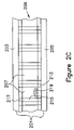
- FIG. 2C is a illustration of a side cross-sectional view of an example embodiment of the flexible display shown in FIG. 2A and FIG. 2B ;
- FIG. 3A is an illustration of example embodiments of an exploded view of a pixel in the off state.
- FIG. 3B is an illustration of example embodiments of an exploded view of a pixel in the on state.
- a display is described herein which is flexible and includes pixels having a magnetically controllable reflectivity.
- the pixels are formed between a pair of flexible non-conductive sheets.
- Each pixel in the display includes a flexible ring that contributes to the flexibility of the display.
- Each of the pixels also includes magnetic particles whose location within the pixel determines the reflectivity of the pixel.
- the display which is described in more detail below, is especially suitable for use in connection with portable electronic devices.
- FIG. 1 is an illustration of an example embodiment of information processing unit 101 including electronic device 103 , display 105 , and take-up bar 107 .
- Take-up bar 107 is connected to electronic device 103 , and display 105 wraps around take-up bar 107 .
- Display 105 is a flexible display capable of being unrolled from take-up bar 107 for viewing.
- Display 105 is electrically coupled to electronic device 103 and is capable of receiving information from electronic device 103 for display. In operation, information is provided to display 105 by electronic device 103 and is viewable after display 103 is extended from take-up bar 105 .
- Packaging flexible display 105 on take-up bar 107 permits electronic device 103 to have both a compact housing and a large display area. A large display area is especially useful in connection with devices used to view e-mail.
- Electronic device 103 is not limited to a particular type of electronic device. Any device capable of providing information to display device 105 is suitable for use in connection with the present invention.
- electronic device 103 is a cellular telephone.
- electronic device 103 is a personal digital assistant.
- electronic device 103 is a calculator.
- electronic device 103 is a geographical positioning system.
- electronic device 103 is a palm size computing device.
- electronic device 103 is a portable web browser.
- FIG. 2A is an illustration of a front view of an example embodiment of display 105 .
- Display 105 in one embodiment, includes a pair of flexible sheets 201 comprising first flexible sheet 203 and second flexible sheet 205 .
- Display 105 also includes pixels 207 located in pixel layer 208 between the pair of flexible sheets 201 .
- Flexible sheets 203 and 205 are preferably fabricated from a flexible dielectric material.
- flexible sheets 203 and 205 are fabricated from thin sheets of polyamide.
- Each one of the pair of flexible sheets 201 has a thickness that allows the pair of flexible sheets 201 to be flexible in a particular application.
- the thickness of each of the pair of flexible sheets 201 is between about 25 micrometers and about 125 micrometers. A thickness of less than 25 micrometers may not provide sufficient structure to ensure long lifetime for flexible sheets 203 and 205 . A thickness of more than about 125 micrometers may not allow for sufficient flexibility in the pair of flexible sheets 201 .
- At least a portion of one of the pair of dielectric sheets 201 is translucent. A translucent sheet permits displaying information as pixels by reflecting light from a material at the back surface of one of the pair of dielectric sheets 201 .
- Pixel layer 208 in one embodiment, is fabricated as a single sheet from a flexible material having a number of holes corresponding to the location of pixels 207 .
- the inner surface of each of the number of holes in one embodiment form a cylinder.
- the inner surface of each of the number of holes form a frustrum.
- the flexibility of pixel layer 208 is improved by having the inner surface of the number of holes form a frustrum.
- Pixel layer 208 may be manufactured using an injection molding process. Prior to the molding operation, a mold for a sheet having a number of holes is fabricated.
- Pixel layer 208 is produced by injecting a material, such as capton, into the mold using an injection molding machine. Fabrication of the present invention is not limited to an injection molding process. Any process capable of producing a flexible pixel layer 208 is also suitable for use in connection with the present invention.
- Pixels 207 are arranged in pixel layer 208 between first flexible sheet 203 and second flexible sheet 205 to form an information display area.
- pixels 207 are arranged in rows and columns to form a rectangular information display area.
- a rectangular information display area may be mapped to an array data structure, which simplifies the tracking of the state of the individual pixels in the information display area.
- each of the pixels 207 in the information display area is individually controllable or addressable and may assume an “on” state or an “off” state. In the “off” state, pixels 207 assumes a first image shade. In the “on”, state pixels 207 assume a second image shade that differs from, and preferably contrasts with, the first image shade. In one embodiment, the first image shade is white and the second image shade is black.
- pixels 207 are turned “on” and “off” to form images. For example, eight pixels 207 are turned “on” to form square 209 in display 105 . In another example, seven pixels 207 are turned “on” to form the letter “I” 211 in display 105 .
- FIG. 2B is an illustration of a back view of an example embodiment of the flexible display shown in FIG. 2A .
- both first flexible sheet 203 and second flexible sheet 205 are translucent.
- FIG. 2A As can be seen by comparing FIG. 2A with FIG. 2B , for a pair sheets 201 that are both translucent, a negative image of the information displayed in FIG. 2A is displayed in FIG. 2B .
- FIG. 2C is an illustration of a cross-sectional side view of an example embodiment of the flexible display shown in FIG. 2A and FIG. 2B .
- Pixel layer 208 including pixels 207 , is formed between the pair of flexible sheets 201 .
- Each of the pixels 207 includes a conductive trace 213 , a non-conductive ring 215 , a second conductive trace 217 , and magnetic particles 219 .
- Conductive traces 213 and 217 are formed on flexible sheets 203 and 205 .
- Non-conductive ring 215 fits between flexible sheets 203 and 205 and is aligned with conductive traces 213 and 217 .
- Non-conductive ring 215 in cooperation with flexible sheets 203 and 205 , encapsulates magnetic particles 219 , and forms a flexible display 105 .
- Conductive traces 213 and 217 are fabricated from conductive materials such as copper, aluminum, silver or gold or alloys of copper, aluminum, silver or gold.
- a layer of conductive material is formed on the surface of flexible sheets 203 and 205 .
- the conductive material is patterned and etched to leave conductive traces 213 and 217 .
- the shape of conductive traces 213 and 217 are selected for ease of fabrication and packing density.
- traces 213 and 217 have a circular shape. A circular shape is easily fabricated, and the corresponding non-conductive ring 215 which preferably matches the shape of traces 213 and 217 is also easily fabricated as a circular cylinder.
- conductive traces 213 and 217 have a hexagonal shape. Conductive traces 213 and 217 have a cross-sectional area sufficient to support a current, without excessive heating, that produces a magnetic field capable of forcing magnetic particles 219 away from the surface on which the conductive trace is formed.
- Non-conductive ring 215 separates flexible sheet 201 from flexible sheet 203 and encloses magnetic particles 219 .
- the flexibility of non-conductive ring 215 affects the flexibility of flexible sheet 203 , so non-conductive ring 215 is preferably fabricated from a flexible material.
- non-conductive ring 215 is fabricated from capton.
- the height of non-conductive ring 215 is selected to allow for contrast between an “on” state and an “off” state in pixels 207 .
- the wall thickness of non-conductive ring 215 is selected to provided structural integrity for the projected life of the flexible display.
- non-conductive ring 215 is generally aligned with conductive traces 213 and 217 , and preferably, the centerline of non-conductive ring 215 is aligned with the centerline of conductive traces 213 and 217 .
- Magnetic particles 219 provide a medium for changing the state of pixels 207 by reflecting light from the back surface of first flexible sheet 203 for a pixel in the “on” state. Therefore, magnetic particles 219 are preferably fabricated from a reflective material. Magnetic particles 219 are also capable of responding to a magnetic field, so magnetic particles 219 are fabricated from a magnetic material. In one embodiment, magnetic particles 219 are fabricated from iron. Magnetic particles 219 , in one embodiment are iron shavings. In an alternate embodiment, magnetic particles 219 are powdered iron. To turn pixels 207 “on” magnetic particles 219 are forced to the back surface of flexible sheet 203 . To turn pixels 207 “off” magnetic particles 219 are forced to the back surface of flexible sheet 205 .
- FIGS. 3A and 3B are illustrations of example embodiments of an exploded view of pixel 207 in the “off” state and the “on” state, respectively.
- Pixel 207 includes conductive traces 213 and 217 formed on the pair of flexible sheets 201 .
- Non-conductive ring 215 is located between the pair of flexible sheets 201 .
- Magnetic particles 219 are enclosed between non-conductive ring 215 and the pair of sheets 201 .
- FIG. 3A also shows magnetic field lines 301 for current 303 flowing in conductive trace 213 .
- the magnetic field associated with magnetic field lines 301 pin magnetic particles 219 at the inner surface of flexible sheet 205 .
- FIG. 3B shows magnetic field lines 307 for current 309 in conductive trace 217 .
- the magnetic field associated with magnetic field lines 307 pin magnetic particles 219 at the inner surface of flexible sheet 203 .
- light entering pixel 207 at flexible sheet 203 is reflected from the back surface of flexible sheet 203 and pixel 207 appears light.
- the display includes a pair of flexible sheets and a number of pixels located between the flexible sheets.
- the number of pixels have a reflectivity that is magnetically controllable.
- a method for fabricating the display includes forming a number of pixels by fabricating traces, an insulating ring, and magnetic particles between a pair of flexible non-conductive sheets.
Abstract
Description
Claims (26)
Priority Applications (8)
| Application Number | Priority Date | Filing Date | Title |
|---|---|---|---|
| US09/539,012 US7158111B1 (en) | 2000-03-30 | 2000-03-30 | Flexible display |
| MYPI20010813A MY134766A (en) | 2000-03-30 | 2001-02-23 | Flexible display |
| CNB018075711A CN1211690C (en) | 2000-03-30 | 2001-03-13 | Flexible display |
| PCT/US2001/008081 WO2001075514A1 (en) | 2000-03-30 | 2001-03-13 | Flexible display |
| KR10-2002-7012903A KR100498193B1 (en) | 2000-03-30 | 2001-03-13 | Flexible display |
| AU2001245692A AU2001245692A1 (en) | 2000-03-30 | 2001-03-13 | Flexible display |
| EP01918639A EP1269249A1 (en) | 2000-03-30 | 2001-03-13 | Flexible display |
| US11/561,068 US7791585B2 (en) | 2000-03-30 | 2006-11-17 | Method of fabricating flexible display |
Applications Claiming Priority (1)
| Application Number | Priority Date | Filing Date | Title |
|---|---|---|---|
| US09/539,012 US7158111B1 (en) | 2000-03-30 | 2000-03-30 | Flexible display |
Related Child Applications (1)
| Application Number | Title | Priority Date | Filing Date |
|---|---|---|---|
| US11/561,068 Division US7791585B2 (en) | 2000-03-30 | 2006-11-17 | Method of fabricating flexible display |
Publications (1)
| Publication Number | Publication Date |
|---|---|
| US7158111B1 true US7158111B1 (en) | 2007-01-02 |
Family
ID=24149378
Family Applications (2)
| Application Number | Title | Priority Date | Filing Date |
|---|---|---|---|
| US09/539,012 Expired - Lifetime US7158111B1 (en) | 2000-03-30 | 2000-03-30 | Flexible display |
| US11/561,068 Expired - Lifetime US7791585B2 (en) | 2000-03-30 | 2006-11-17 | Method of fabricating flexible display |
Family Applications After (1)
| Application Number | Title | Priority Date | Filing Date |
|---|---|---|---|
| US11/561,068 Expired - Lifetime US7791585B2 (en) | 2000-03-30 | 2006-11-17 | Method of fabricating flexible display |
Country Status (7)
| Country | Link |
|---|---|
| US (2) | US7158111B1 (en) |
| EP (1) | EP1269249A1 (en) |
| KR (1) | KR100498193B1 (en) |
| CN (1) | CN1211690C (en) |
| AU (1) | AU2001245692A1 (en) |
| MY (1) | MY134766A (en) |
| WO (1) | WO2001075514A1 (en) |
Cited By (13)
| Publication number | Priority date | Publication date | Assignee | Title |
|---|---|---|---|---|
| US20040233176A1 (en) * | 2003-05-23 | 2004-11-25 | Bar-Long Denq | Touch panel with magnetic display unit |
| US20060166713A1 (en) * | 2005-01-25 | 2006-07-27 | Wistron Corporation | Electronic device having an adjustable display area |
| US20070092689A1 (en) * | 2000-03-30 | 2007-04-26 | Intel Corporation | Method of fabricating flexible display |
| US20080024976A1 (en) * | 2006-02-06 | 2008-01-31 | Hardson Winston B | Digital video and music player belt buckles |
| US20080086925A1 (en) * | 2006-10-12 | 2008-04-17 | Samsung Electronics Co., Ltd. | Flexible display unit mobile terminal having the same |
| US20080167095A1 (en) * | 2007-01-05 | 2008-07-10 | Samsung Electronics Co., Ltd. | Folder-type portable communication device having flexible display unit |
| US20080290683A1 (en) * | 2006-02-21 | 2008-11-27 | Benecke-Kaliko Ag | Plastic Skin with Switching Function |
| US20100064564A1 (en) * | 2006-10-31 | 2010-03-18 | Polymer Vision Limited | Flexible display supported by hinged frame |
| US20110227240A1 (en) * | 2008-08-29 | 2011-09-22 | Stefan Sostmann | Molded skin with electroluminescent elements |
| US20120182677A1 (en) * | 2011-01-18 | 2012-07-19 | Pantech Co., Ltd. | Portable terminal transformable into bracelet |
| US20150009613A1 (en) * | 2013-07-08 | 2015-01-08 | Kabushiki Kaisha Toshiba | Electronic device |
| US10744814B1 (en) * | 2018-05-17 | 2020-08-18 | Anton Zumot | Etch a sketch tool with removable and replacable glasses and method thereof |
| US10788863B1 (en) * | 2019-04-16 | 2020-09-29 | Wuhan China Star Optoelectronics Semiconductor Display Technology Co., Ltd. | Flexible display device |
Families Citing this family (3)
| Publication number | Priority date | Publication date | Assignee | Title |
|---|---|---|---|---|
| KR100795796B1 (en) * | 2006-04-03 | 2008-01-21 | 삼성에스디아이 주식회사 | Panel for plasma display, method of manufacturing the panel, plasma display panel comprising the panel, and method of manufacturing the panel |
| WO2009067010A2 (en) * | 2007-11-21 | 2009-05-28 | Polymer Vision Limited | An electronic device with a flexible display |
| CN105450415B (en) * | 2014-08-28 | 2019-06-14 | 阿里巴巴集团控股有限公司 | Safe checking method and equipment |
Citations (27)
| Publication number | Priority date | Publication date | Assignee | Title |
|---|---|---|---|---|
| US3670323A (en) | 1970-12-14 | 1972-06-13 | Zenith Radio Corp | Image-display devices comprising particle light modulators with storage |
| US3760505A (en) | 1971-11-17 | 1973-09-25 | Ohio Art Co | Tracing device |
| WO1990010291A1 (en) | 1989-02-23 | 1990-09-07 | Remote Image Systems Limited | Re-usable information recording sheet material |
| EP0633488A1 (en) | 1993-07-05 | 1995-01-11 | Kabushikigaisya KEIOU | Magnetic fluid display, image display controlling apparatus for the magnetic fluid display, and method of making the same |
| US5411398A (en) | 1992-05-29 | 1995-05-02 | Japan Capsular Products, Inc. | Magnetic display system |
| US5467107A (en) | 1993-10-01 | 1995-11-14 | Copytele, Inc. | Electrophoretic display panel with selective character addressability |
| US5469020A (en) * | 1994-03-14 | 1995-11-21 | Massachusetts Institute Of Technology | Flexible large screen display having multiple light emitting elements sandwiched between crossed electrodes |
| US5659330A (en) | 1996-05-31 | 1997-08-19 | Xerox Corporation | Electrocapillary color display sheet |
| US5739887A (en) * | 1994-10-21 | 1998-04-14 | Hitachi, Ltd. | Liquid crystal display device with reduced frame portion surrounding display area |
| US5754329A (en) | 1992-12-22 | 1998-05-19 | Monsanto Company | Electrochromic display laminates |
| US5754332A (en) | 1996-06-27 | 1998-05-19 | Xerox Corporation | Monolayer gyricon display |
| JPH10257143A (en) | 1997-02-21 | 1998-09-25 | Nokia Mobile Phones Ltd | Mobile communication equipment |
| US5859722A (en) | 1995-07-04 | 1999-01-12 | Nippom Oil Co., Ltd | Electrochromic device |
| US5931764A (en) | 1998-06-24 | 1999-08-03 | Viztec, Inc. | Wearable device with flexible display |
| WO2000013156A1 (en) | 1998-08-26 | 2000-03-09 | Addco, Inc. | Outdoor changeable message sign with protective layers |
| US6235395B1 (en) * | 1998-03-05 | 2001-05-22 | Xerox Corporation | Flexible displays comprising spheres encapsulated within a wax |
| US6262706B1 (en) * | 1995-07-20 | 2001-07-17 | E Ink Corporation | Retroreflective electrophoretic displays and materials for making the same |
| US6271823B1 (en) * | 1998-09-16 | 2001-08-07 | International Business Machines Corporation | Reflective electrophoretic display with laterally adjacent color cells using a reflective panel |
| US6281038B1 (en) * | 1999-02-05 | 2001-08-28 | Alien Technology Corporation | Methods for forming assemblies |
| US6310675B1 (en) * | 1997-12-22 | 2001-10-30 | Zvi Yaniv | Liquid crystal display |
| US6330054B1 (en) * | 1998-09-30 | 2001-12-11 | Brother Kogyo Kabushiki Kaisha | Image-forming method and image-forming apparatus on recording medium including microcapsules |
| US6340965B1 (en) * | 1999-03-18 | 2002-01-22 | Xerox Corporation | Modifiable display having fixed image patterns |
| US6498597B1 (en) * | 1998-10-28 | 2002-12-24 | Fuji Photo Film Co., Ltd. | Continuously displayable scroll-type display |
| EP1269249A1 (en) | 2000-03-30 | 2003-01-02 | Intel Corporation | Flexible display |
| US6504524B1 (en) * | 2000-03-08 | 2003-01-07 | E Ink Corporation | Addressing methods for displays having zero time-average field |
| US6629847B1 (en) * | 1998-07-31 | 2003-10-07 | Takara Co., Ltd. | Magnetic display panel and method for producing the same |
| US6639579B1 (en) * | 1998-10-16 | 2003-10-28 | Takara Corporation Limited | Magnetophoresis type display device and process of production of same |
Family Cites Families (11)
| Publication number | Priority date | Publication date | Assignee | Title |
|---|---|---|---|---|
| US3322482A (en) * | 1965-04-12 | 1967-05-30 | James V Harmon | Panel for controlling light transmission by the selective orientation of free particles |
| US4139841A (en) | 1977-06-22 | 1979-02-13 | E-Systems, Inc. | Electromagnetic information display system |
| GB2292119B (en) * | 1994-08-10 | 1998-12-30 | Chemitech Inc | A process for producing a magnetic display sheet using microcapsules |
| US5922268A (en) * | 1997-10-30 | 1999-07-13 | Xerox Corporation | Method of manufacturing a twisting cylinder display using multiple chromatic values |
| JPH10123987A (en) * | 1996-10-21 | 1998-05-15 | Star Micronics Co Ltd | Magnetic head for magnetic display |
| US6839158B2 (en) * | 1997-08-28 | 2005-01-04 | E Ink Corporation | Encapsulated electrophoretic displays having a monolayer of capsules and materials and methods for making the same |
| DE69918308T2 (en) * | 1998-04-10 | 2004-10-21 | E Ink Corp | ELECTRONIC DISPLAY BASED ON ORGANIC FIELD EFFECT TRANSISTORS |
| US6924781B1 (en) * | 1998-09-11 | 2005-08-02 | Visible Tech-Knowledgy, Inc. | Smart electronic label employing electronic ink |
| US6724519B1 (en) * | 1998-12-21 | 2004-04-20 | E-Ink Corporation | Protective electrodes for electrophoretic displays |
| US6316278B1 (en) * | 1999-03-16 | 2001-11-13 | Alien Technology Corporation | Methods for fabricating a multiple modular assembly |
| US6456272B1 (en) * | 1999-11-12 | 2002-09-24 | Xerox Corporation | Field addressed displays using charge discharging in conjunction with charge retaining island structures |
-
2000
- 2000-03-30 US US09/539,012 patent/US7158111B1/en not_active Expired - Lifetime
-
2001
- 2001-02-23 MY MYPI20010813A patent/MY134766A/en unknown
- 2001-03-13 AU AU2001245692A patent/AU2001245692A1/en not_active Abandoned
- 2001-03-13 WO PCT/US2001/008081 patent/WO2001075514A1/en active IP Right Grant
- 2001-03-13 CN CNB018075711A patent/CN1211690C/en not_active Expired - Lifetime
- 2001-03-13 KR KR10-2002-7012903A patent/KR100498193B1/en active IP Right Grant
- 2001-03-13 EP EP01918639A patent/EP1269249A1/en not_active Withdrawn
-
2006
- 2006-11-17 US US11/561,068 patent/US7791585B2/en not_active Expired - Lifetime
Patent Citations (29)
| Publication number | Priority date | Publication date | Assignee | Title |
|---|---|---|---|---|
| US3670323A (en) | 1970-12-14 | 1972-06-13 | Zenith Radio Corp | Image-display devices comprising particle light modulators with storage |
| US3760505A (en) | 1971-11-17 | 1973-09-25 | Ohio Art Co | Tracing device |
| WO1990010291A1 (en) | 1989-02-23 | 1990-09-07 | Remote Image Systems Limited | Re-usable information recording sheet material |
| US5411398A (en) | 1992-05-29 | 1995-05-02 | Japan Capsular Products, Inc. | Magnetic display system |
| US5754329A (en) | 1992-12-22 | 1998-05-19 | Monsanto Company | Electrochromic display laminates |
| EP0633488A1 (en) | 1993-07-05 | 1995-01-11 | Kabushikigaisya KEIOU | Magnetic fluid display, image display controlling apparatus for the magnetic fluid display, and method of making the same |
| JPH07146659A (en) | 1993-07-05 | 1995-06-06 | Aiki Denko Kk | Magnetic fluid display, image display controller of magnetic fluid display and its production |
| US5467107A (en) | 1993-10-01 | 1995-11-14 | Copytele, Inc. | Electrophoretic display panel with selective character addressability |
| US5469020A (en) * | 1994-03-14 | 1995-11-21 | Massachusetts Institute Of Technology | Flexible large screen display having multiple light emitting elements sandwiched between crossed electrodes |
| US5838400A (en) * | 1994-10-21 | 1998-11-17 | Hitachi, Ltd. | Liquid crystal display device with reduced frame portion surrounding display area |
| US5739887A (en) * | 1994-10-21 | 1998-04-14 | Hitachi, Ltd. | Liquid crystal display device with reduced frame portion surrounding display area |
| US5859722A (en) | 1995-07-04 | 1999-01-12 | Nippom Oil Co., Ltd | Electrochromic device |
| US6262706B1 (en) * | 1995-07-20 | 2001-07-17 | E Ink Corporation | Retroreflective electrophoretic displays and materials for making the same |
| US5659330A (en) | 1996-05-31 | 1997-08-19 | Xerox Corporation | Electrocapillary color display sheet |
| US5754332A (en) | 1996-06-27 | 1998-05-19 | Xerox Corporation | Monolayer gyricon display |
| JPH10257143A (en) | 1997-02-21 | 1998-09-25 | Nokia Mobile Phones Ltd | Mobile communication equipment |
| US6310675B1 (en) * | 1997-12-22 | 2001-10-30 | Zvi Yaniv | Liquid crystal display |
| US6235395B1 (en) * | 1998-03-05 | 2001-05-22 | Xerox Corporation | Flexible displays comprising spheres encapsulated within a wax |
| US5931764A (en) | 1998-06-24 | 1999-08-03 | Viztec, Inc. | Wearable device with flexible display |
| US6629847B1 (en) * | 1998-07-31 | 2003-10-07 | Takara Co., Ltd. | Magnetic display panel and method for producing the same |
| WO2000013156A1 (en) | 1998-08-26 | 2000-03-09 | Addco, Inc. | Outdoor changeable message sign with protective layers |
| US6271823B1 (en) * | 1998-09-16 | 2001-08-07 | International Business Machines Corporation | Reflective electrophoretic display with laterally adjacent color cells using a reflective panel |
| US6330054B1 (en) * | 1998-09-30 | 2001-12-11 | Brother Kogyo Kabushiki Kaisha | Image-forming method and image-forming apparatus on recording medium including microcapsules |
| US6639579B1 (en) * | 1998-10-16 | 2003-10-28 | Takara Corporation Limited | Magnetophoresis type display device and process of production of same |
| US6498597B1 (en) * | 1998-10-28 | 2002-12-24 | Fuji Photo Film Co., Ltd. | Continuously displayable scroll-type display |
| US6281038B1 (en) * | 1999-02-05 | 2001-08-28 | Alien Technology Corporation | Methods for forming assemblies |
| US6340965B1 (en) * | 1999-03-18 | 2002-01-22 | Xerox Corporation | Modifiable display having fixed image patterns |
| US6504524B1 (en) * | 2000-03-08 | 2003-01-07 | E Ink Corporation | Addressing methods for displays having zero time-average field |
| EP1269249A1 (en) | 2000-03-30 | 2003-01-02 | Intel Corporation | Flexible display |
Non-Patent Citations (1)
| Title |
|---|
| Scientific American (Cover Illustration), 1 p., (Nov. 2000). |
Cited By (23)
| Publication number | Priority date | Publication date | Assignee | Title |
|---|---|---|---|---|
| US20070092689A1 (en) * | 2000-03-30 | 2007-04-26 | Intel Corporation | Method of fabricating flexible display |
| US7791585B2 (en) | 2000-03-30 | 2010-09-07 | Intel Corporation | Method of fabricating flexible display |
| US20040233176A1 (en) * | 2003-05-23 | 2004-11-25 | Bar-Long Denq | Touch panel with magnetic display unit |
| US20090073139A1 (en) * | 2003-05-23 | 2009-03-19 | Bar-Long Denq | Touch panel with magnetic display unit |
| US20060166713A1 (en) * | 2005-01-25 | 2006-07-27 | Wistron Corporation | Electronic device having an adjustable display area |
| US7426107B2 (en) * | 2005-01-25 | 2008-09-16 | Wistron Corporation | Electronic device having an adjustable display area |
| US7848093B2 (en) * | 2006-02-06 | 2010-12-07 | Hardson Winston B | Digital video and music player belt buckles |
| US20080024976A1 (en) * | 2006-02-06 | 2008-01-31 | Hardson Winston B | Digital video and music player belt buckles |
| US20080290683A1 (en) * | 2006-02-21 | 2008-11-27 | Benecke-Kaliko Ag | Plastic Skin with Switching Function |
| US7954874B2 (en) * | 2006-02-21 | 2011-06-07 | Benecke-Kaliko Ag | Plastic skin with switching function |
| US20080086925A1 (en) * | 2006-10-12 | 2008-04-17 | Samsung Electronics Co., Ltd. | Flexible display unit mobile terminal having the same |
| US7636085B2 (en) * | 2006-10-12 | 2009-12-22 | Samsung Electronics Co., Ltd | Flexible display unit mobile terminal having the same |
| US8151501B2 (en) * | 2006-10-31 | 2012-04-10 | Creator Technology B.V. | Flexible display supported by hinged frame |
| US20100064564A1 (en) * | 2006-10-31 | 2010-03-18 | Polymer Vision Limited | Flexible display supported by hinged frame |
| US20080167095A1 (en) * | 2007-01-05 | 2008-07-10 | Samsung Electronics Co., Ltd. | Folder-type portable communication device having flexible display unit |
| US8229522B2 (en) | 2007-01-05 | 2012-07-24 | Samsung Electronics Co., Ltd. | Folder-type portable communication device having flexible display unit |
| US20110227240A1 (en) * | 2008-08-29 | 2011-09-22 | Stefan Sostmann | Molded skin with electroluminescent elements |
| US8377347B2 (en) * | 2008-08-29 | 2013-02-19 | Johnson Controls Interiors Gmbh & Co. Kg | Molded skin with electroluminescent elements |
| US20120182677A1 (en) * | 2011-01-18 | 2012-07-19 | Pantech Co., Ltd. | Portable terminal transformable into bracelet |
| US20150009613A1 (en) * | 2013-07-08 | 2015-01-08 | Kabushiki Kaisha Toshiba | Electronic device |
| US9141143B2 (en) * | 2013-07-08 | 2015-09-22 | Kabushiki Kaisha Toshiba | Electronic device |
| US10744814B1 (en) * | 2018-05-17 | 2020-08-18 | Anton Zumot | Etch a sketch tool with removable and replacable glasses and method thereof |
| US10788863B1 (en) * | 2019-04-16 | 2020-09-29 | Wuhan China Star Optoelectronics Semiconductor Display Technology Co., Ltd. | Flexible display device |
Also Published As
| Publication number | Publication date |
|---|---|
| KR100498193B1 (en) | 2005-06-29 |
| AU2001245692A1 (en) | 2001-10-15 |
| MY134766A (en) | 2007-12-31 |
| WO2001075514A1 (en) | 2001-10-11 |
| US7791585B2 (en) | 2010-09-07 |
| CN1211690C (en) | 2005-07-20 |
| CN1429351A (en) | 2003-07-09 |
| EP1269249A1 (en) | 2003-01-02 |
| US20070092689A1 (en) | 2007-04-26 |
| KR20020081594A (en) | 2002-10-28 |
Similar Documents
| Publication | Publication Date | Title |
|---|---|---|
| US7791585B2 (en) | Method of fabricating flexible display | |
| US10708482B2 (en) | Terminal having camera module | |
| US7019714B2 (en) | Mobile terminal provided with organic electroluminescent and liquid crystal devices | |
| KR100607378B1 (en) | Visual alarm for a communication module | |
| KR101019138B1 (en) | Display and electronic device | |
| CN111063720B (en) | Display panel and display device | |
| US7903083B2 (en) | Mixed-mode encapsulated electrophoretic display for electronic device | |
| US8369890B2 (en) | Mobile electronic device with an illuminated static display | |
| US7170506B2 (en) | Hybrid electronic display of light emissive display elements and light reflective display elements | |
| CN110649074A (en) | Display panel and display device | |
| JP2007047714A (en) | Display module and cellular phone set and electronic apparatus having the same | |
| KR20020032362A (en) | Wiring substrate, display device, semiconductor chip, and electronic equipment | |
| JP2008527427A (en) | General-purpose display module | |
| CN110740592A (en) | Shell and electronic equipment | |
| JP2002366059A (en) | Portable information terminal | |
| CN113655646B (en) | Display panel, display module and display device | |
| US20230320155A1 (en) | Display panel and display device | |
| CN109492468A (en) | Display module and its manufacturing method and electronic device | |
| CN212874736U (en) | Middle frame assembly, antenna device and electronic equipment | |
| JP2004192314A (en) | Ic card with information display means and its manufacturing method | |
| WO2023226608A1 (en) | Electronic device | |
| CN212433746U (en) | Color film touch display panel and display device | |
| CN217767138U (en) | Display panel and display device | |
| KR101655805B1 (en) | Mobile terminal | |
| CN218004798U (en) | Light emitting diode chip and light emitting diode display panel |
Legal Events
| Date | Code | Title | Description |
|---|---|---|---|
| AS | Assignment |
Owner name: INTEL CORPORATION, CALIFORNIA Free format text: ASSIGNMENT OF ASSIGNORS INTEREST;ASSIGNORS:JACKSON, JAMES D.;DISHONGH, TERRANCE J.;SEARLS, DAMION T.;REEL/FRAME:010989/0005;SIGNING DATES FROM 20000512 TO 20000601 |
|
| STCF | Information on status: patent grant |
Free format text: PATENTED CASE |
|
| REMI | Maintenance fee reminder mailed | ||
| FPAY | Fee payment |
Year of fee payment: 4 |
|
| SULP | Surcharge for late payment | ||
| FPAY | Fee payment |
Year of fee payment: 8 |
|
| FEPP | Fee payment procedure |
Free format text: PAYOR NUMBER ASSIGNED (ORIGINAL EVENT CODE: ASPN); ENTITY STATUS OF PATENT OWNER: LARGE ENTITY |
|
| MAFP | Maintenance fee payment |
Free format text: PAYMENT OF MAINTENANCE FEE, 12TH YEAR, LARGE ENTITY (ORIGINAL EVENT CODE: M1553) Year of fee payment: 12 |