US7115853B2 - Micro-lens configuration for small lens focusing in digital imaging devices - Google Patents

Micro-lens configuration for small lens focusing in digital imaging devices Download PDF

Info

Publication number
US7115853B2
US7115853B2 US10/667,390 US66739003A US7115853B2 US 7115853 B2 US7115853 B2 US 7115853B2 US 66739003 A US66739003 A US 66739003A US 7115853 B2 US7115853 B2 US 7115853B2
Authority
US
United States
Prior art keywords
micro
lens
sacrificial material
sacrificial
molds
Prior art date
Legal status (The legal status is an assumption and is not a legal conclusion. Google has not performed a legal analysis and makes no representation as to the accuracy of the status listed.)
Expired - Lifetime, expires
Application number
US10/667,390
Other versions
US20050061950A1 (en
Inventor
Tongbi Jiang
Michael Connell
Jin Li
Current Assignee (The listed assignees may be inaccurate. Google has not performed a legal analysis and makes no representation or warranty as to the accuracy of the list.)
Aptina Imaging Corp
Original Assignee
Micron Technology Inc
Priority date (The priority date is an assumption and is not a legal conclusion. Google has not performed a legal analysis and makes no representation as to the accuracy of the date listed.)
Filing date
Publication date
Application filed by Micron Technology Inc filed Critical Micron Technology Inc
Priority to US10/667,390 priority Critical patent/US7115853B2/en
Assigned to MICRON TECHNOLOGY, INC. reassignment MICRON TECHNOLOGY, INC. ASSIGNMENT OF ASSIGNORS INTEREST (SEE DOCUMENT FOR DETAILS). Assignors: CONNELL, MICHAEL, JIANG, TONGBI, LI, JIN
Publication of US20050061950A1 publication Critical patent/US20050061950A1/en
Priority to US11/257,039 priority patent/US7405385B2/en
Priority to US11/257,041 priority patent/US7557337B2/en
Application granted granted Critical
Publication of US7115853B2 publication Critical patent/US7115853B2/en
Assigned to APTINA IMAGING CORPORATION reassignment APTINA IMAGING CORPORATION ASSIGNMENT OF ASSIGNORS INTEREST (SEE DOCUMENT FOR DETAILS). Assignors: MICRON TECHNOLOGY, INC.
Adjusted expiration legal-status Critical
Expired - Lifetime legal-status Critical Current

Links

Images

Classifications

    • HELECTRICITY
    • H01ELECTRIC ELEMENTS
    • H01LSEMICONDUCTOR DEVICES NOT COVERED BY CLASS H10
    • H01L27/00Devices consisting of a plurality of semiconductor or other solid-state components formed in or on a common substrate
    • H01L27/14Devices consisting of a plurality of semiconductor or other solid-state components formed in or on a common substrate including semiconductor components sensitive to infrared radiation, light, electromagnetic radiation of shorter wavelength or corpuscular radiation and specially adapted either for the conversion of the energy of such radiation into electrical energy or for the control of electrical energy by such radiation
    • H01L27/144Devices controlled by radiation
    • H01L27/146Imager structures
    • H01L27/14601Structural or functional details thereof
    • H01L27/14625Optical elements or arrangements associated with the device
    • H01L27/14627Microlenses
    • BPERFORMING OPERATIONS; TRANSPORTING
    • B33ADDITIVE MANUFACTURING TECHNOLOGY
    • B33YADDITIVE MANUFACTURING, i.e. MANUFACTURING OF THREE-DIMENSIONAL [3-D] OBJECTS BY ADDITIVE DEPOSITION, ADDITIVE AGGLOMERATION OR ADDITIVE LAYERING, e.g. BY 3-D PRINTING, STEREOLITHOGRAPHY OR SELECTIVE LASER SINTERING
    • B33Y80/00Products made by additive manufacturing

Definitions

  • the present invention relates generally to micro-lenses for imager devices and to methods for producing the same.
  • Image sensing devices i.e., image sensors
  • image sensors that employ light detecting elements (e.g., photo sensors) for use in various applications such as in semiconductor devices.
  • image sensors may be formed using a variety of fabrication techniques.
  • CMOS image sensors two commonly fabricated image sensors are CMOS image sensors and charge coupled device (CCD) image sensors.
  • CCD charge coupled device
  • Each generally includes an array of pixels containing the photo sensors.
  • the image sensors typically use photo sensors in the form of photogates, phototransistors or photodiodes.
  • each micro-lens may be used to direct incoming light through a circuitry region of the corresponding pixel to the photo sensor region, thereby increasing the amount of light reaching the photo sensor and thereby increasing the fill factor of the pixels.
  • Each photo sensor is located at a suitable depth in the image sensor such that light, when collimated and focused by a corresponding micro-lens of a given focal length, is directed onto the photo sensor.
  • micro-lens arrays examples include intensifying illuminating light from pixels of a non-luminescent display device (such as a liquid crystal display device) to increase the brightness of the display, forming an image to be printed in a liquid crystal or light emitting diode printer, and providing focusing for coupling a luminescent device or a receptive device to an optical fiber.
  • a non-luminescent display device such as a liquid crystal display device
  • each pixel in the imager array produces a signal corresponding to the intensity of light impinging on the photo sensor associated with that pixel.
  • the magnitude of the signal produced is approximately proportional to the amount of light impinging on the photo sensor.
  • the signals may be used, for example, to display a corresponding image on a monitor or to otherwise provide information about the optical image.
  • the micro-lens arrays must be made smaller as well.
  • the focal length of the micro-lens is reduced. This reduced focal length causes light to be focused at a reduced depth in the image sensor device.
  • the depth of the photo sensors is reduced in the substrate to correspond to the reduced focal length of the micro-lenses. Decreasing the photo sensor's depth in the substrate, however, requires manufacturing changes, and results in additional effort, expense and time in processing.
  • micro-lenses use patterning and reflow techniques that are typically used to produce convex micro-lenses. These fabrication techniques are difficult to tailor to produce micro-lenses that direct light to a particular focal point when the micro-lens size and geometry (and resultant focal length) change.
  • a passivation layer such as a silicon nitride passivation layer separates the color filters from the photo sensors. This passivation layer causes undesirable reflection in the optical path to the photo sensors.
  • an image sensor having micro-lenses formed to focus light onto the photo sensors of the image sensor such that the depth of the photo sensors does not have to be decreased even when the image sensor device, including its photo sensors and micro-lenses, decreases in size.
  • the present invention provides micro-lenses formed to focus light onto the photo sensors of the image sensor such that the depth of the photo sensors does not have to be decreased even when the image sensor device, including its photo sensors and micro-lenses, decrease in size.
  • an image sensor includes a first micro-lens array of one or more first micro-lenses for collimating (i.e., capturing) incoming light and a second micro-lens array of one or more second micro-lenses for focusing the light onto a photo sensor.
  • the second micro-lens array is separated from the first micro-lens array by a cavity.
  • the second micro-lens array and first micro-lens array are positioned relative to one another such that incoming light is collimated (i.e., captured) by a first micro-lens of the first micro-lens array, and then directed through the cavity to a second micro-lens of the second micro-lens array, which focuses the incoming light onto a corresponding photo sensor.
  • the cavity that separates the second micro-lens array from the first micro-lens array consists of an air gap.
  • an image sensor in another embodiment, includes a first micro-lens array of one or more first micro-lenses for colliminating (i.e., capturing) and focusing incoming light onto a photo sensor.
  • the first micro-lens array is separated from the upper-most layers of the semiconductor substrate by a cavity.
  • the image sensor may further include supports in the form of posts, or in the form of other structures such as walls, to support the upper layers of the image sensor, including the image sensor layers above the cavity, relative to the lower layers of the image sensor.
  • the supports may be located at any suitable location in the image sensor such as at the edges of the image sensor or at locations interior of the edges of the image sensor.
  • a first of at least two arrays of micro-lenses maybe formed by coating a semiconductor substrate with a layer of second micro-lens material and a lower photo resist. Lower layer openings are developed in the photo resist. The second micro-lens material is then etched to form a second micro-lens array. A sacrificial material is applied to the second micro-lens array. Lens molds and one or more support molds are formed in the sacrificial material. Supports are formed by filling the support molds with a support material that is at least substantially non-reflective and that is of sufficient strength to support the upper layers of the image sensor.
  • the first micro-lens array is formed by applying a layer of first micro-lens material to the sacrificial material to fill the lens molds formed in the sacrificial material.
  • the sacrificial material is removed from the image sensor by a suitable method (such as by heating or chemical removal) leaving a cavity between the second micro-lens array and the first micro-lens array.
  • the sacrificial material is degraded by heat or chemical treatment, and, as it degrades, the sacrificial material diffuses through the micro-lens material.
  • additional clean techniques are applied to remove residual particles through vacuum channels formed in the image sensor.
  • the sacrificial material may be removed, such as through heat or chemical treatment. Residual sacrificial material remaining after such treatment may be removed by vacuuming through the vacuum channels.
  • the vacuum channels may also be used to vacuum remove other residual particles, such as residual chemicals that may remain after a chemical removal treatment.
  • a color filter array may be applied to the first-most micro-lens material of the present invention.
  • a color filter may be applied on top of the first micro-lens array. Additional coatings, for example protective coatings, may also be applied on top of the color filter array.
  • the color filter may also be applied at alternative locations, for example below the second micro-lens array (i.e., the color filter array may be applied to the upper layers of the substrate before applying the second micro-lens material).
  • an image sensor having a first micro-lens array for collimating and focusing incoming light onto a photo sensor.
  • the first micro-lens of the array may be formed by coating a semiconductor substrate with a layer of sacrificial material.
  • Lens molds and support molds are formed in the sacrificial material.
  • Supports are formed by filling the support molds with a support material that is at least substantially non-reflective and sufficiently strong enough to support the upper layers of the image sensor.
  • a layer of first micro-lens material is applied to the sacrificial material to fill the lens molds and form the first micro-lens array.
  • the supports be made of the first micro-lens material and be formed at the same time as the first micro-lens array by applying the first micro-lens material.
  • the sacrificial material may be removed by heating or chemical treatment. If necessary, one or more vacuum channels may be formed in the image sensor through which residual particles (e.g., sacrificial material or residual chemical solvents) may be removed.
  • a sacrificial material in the present invention allows fabrication of micro-lenses of a desired focal length such that light may be directed to corresponding photo sensors at a desired depth in a semiconductor substrate.
  • the geometry of the micro-lenses fabricated using the sacrificial material lens molds can be formed to a variety of shapes.
  • the micro-lenses formed according to the invention have a concave shape.
  • Concave micro-lenses may provide improved light capture, such as for example where the edges of the micro-lenses of a given micro-lens array touch or overlap in the surface plane of the array.
  • the image sensor may be constructed without a passivation layer between the color filter array and the photo sensors where the cavity of the image sensor is positioned between the color filter array the photo sensors (such as where the color filter array is formed above the cavity).
  • FIG. 1 is an enlarged cross-sectional view of a conventional image sensor including photo sensors, color filters and multiple micro-lenses formed thereon;
  • FIG. 2 is an enlarged cross-sectional view of the conventional image sensor of FIG. 1 , reduced in size including photo sensors, color filters and micro-lenses of reduced size;
  • FIG. 3 is an enlarged cross-sectional view, in accordance with an exemplary embodiment of the invention, of an image sensor including photo sensors, color filters and multiple micro-lens arrays formed thereon;
  • FIG. 3 a is plan view of an exemplary embodiment of the image sensor device of the invention having support walls;
  • FIG. 3 b is an enlarged cross-sectional view of an exemplary embodiment of the image sensor device of the invention having supports located internal of the edges of the image sensor;
  • FIG. 4 is an enlarged cross-sectional view, in accordance with an exemplary embodiment of the invention, of an image sensor including photo sensors, color filters and a single micro-lens array formed thereon;
  • FIG. 5 a is an enlarged cross-sectional view of the embodiment of the image sensor of FIG. 3 during fabrication, having a second micro-lens material applied;
  • FIG. 5 b is an enlarged cross-sectional view of the embodiment of the image sensor of FIG. 3 during fabrication, having second micro-lenses formed therein;
  • FIG. 5 c is an enlarged cross-sectional view of the embodiment of the image sensor of FIG. 3 during fabrication, having a sacrificial material applied;
  • FIG. 5 d is an enlarged cross-sectional view of the embodiment of the image sensor of FIG. 3 during fabrication, having a support openings and sacrificial resist openings formed therein;
  • FIG. 5 e is an enlarged cross-sectional view of the embodiment of the image sensor of FIG. 3 during fabrication, having support molds formed therein;
  • FIG. 5 f is an enlarged cross-sectional view of the embodiment of the image sensor of FIG. 3 during fabrication, having lens molds formed therein;
  • FIG. 5 g is an enlarged cross-sectional view of the embodiment of the image sensor of FIG. 3 during fabrication, having a first micro-lens array and supports formed therein;
  • FIG. 5 h is an enlarged cross-sectional view of the embodiment of the image sensor of FIG. 3 during fabrication, having a first micro-lens array and supports formed therein of different materials;
  • FIG. 5 i is an enlarged cross-sectional view of the first micro-lens array and second micro-lens array of an embodiment of the image sensor of FIG. 3 during fabrication, having sacrificial material exposed at a side plane;
  • FIG. 6 a is an enlarged cross-sectional view of a stage of fabrication of vacuum channels for an image sensor, having a vacuum photo resist applied thereto;
  • FIG. 6 b is an enlarged cross-sectional view of a stage of fabrication of vacuum channels for an image sensor, having vacuum openings formed therein;
  • FIG. 6 c is an enlarged cross-sectional view of a stage of fabrication of vacuum channels for an image sensor, having vacuum channels formed therein;
  • FIG. 6 d is an enlarged cross-sectional view of a stage of fabrication of vacuum channels for an image sensor, having plugged vacuum channels;
  • FIG. 7 a is an enlarged cross-sectional view of the embodiment of the image sensor of FIG. 4 during fabrication, having a substrate provided;
  • FIG. 7 b is an enlarged cross-sectional view of the embodiment of the image sensor of FIG. 4 during fabrication, having a sacrificial material applied;
  • FIG. 7 c is an enlarged cross-sectional view of the embodiment of the image sensor of FIG. 4 during fabrication, having a sacrificial photo resist applied;
  • FIG. 7 d is an enlarged cross-sectional view of the embodiment of the image sensor of FIG. 4 during fabrication, having a sacrificial resist openings, and support openings formed therein;
  • FIG. 7 e is an enlarged cross-sectional view of the embodiment of the image sensor of FIG. 4 during fabrication, having a support mold formed therein;
  • FIG. 7 f is an enlarged cross-sectional view of the embodiment of the image sensor of FIG. 4 during fabrication, having lens molds formed therein;
  • FIG. 7 g is an enlarged cross-sectional view of the embodiment of the image sensor of FIG. 4 during fabrication, having a first micro-lens array and supports formed therein;
  • FIG. 8 a is an enlarged cross-sectional view of a stage of fabrication of an image sensor having a sacrificial resist applied thereto;
  • FIG. 8 b is an enlarged cross-sectional view of a stage of fabrication of an image sensor, having a lens molds and support molds formed therein;
  • FIG. 9 a is an enlarged cross-sectional view of lens molds formed during fabrication of micro-lenses
  • FIG. 9 b is an enlarged cross-sectional view of the lens molds of FIG. 9 a increased in widths
  • FIG. 10 is an enlarged cross-sectional view of an exemplary embodiment of the invention, having convex lens
  • FIG. 10 a is an enlarged cross-sectional view of the embodiment of the image sensor of FIG. 10 during fabrication, having a sacrificial resist applied thereto;
  • FIG. 10 b is an enlarged cross-sectional view of the embodiment of the image sensor of FIG. 10 during fabrication, having convex lens molds formed therein;
  • FIG. 10 c is an enlarged cross-sectional view of the embodiment of the image sensor of FIG. 10 during fabrication, having a first micro-lens array formed thereon;
  • FIG. 11 is a schematic diagram of a processor system incorporating an image sensor comprising a plurality of micro-lenses constructed in accordance with an exemplary embodiment of the invention.
  • wafer and substrate are to be understood as interchangeable and as including silicon, silicon-on-insulator (SOI) or silicon-on-sapphire (SOS), doped and undoped semiconductors, epitaxial layers of silicon supported by a base semiconductor foundation, and other semiconductor structures.
  • SOI silicon-on-insulator
  • SOS silicon-on-sapphire
  • doped and undoped semiconductors epitaxial layers of silicon supported by a base semiconductor foundation, and other semiconductor structures.
  • previous process steps may have been utilized to form regions, junctions or material layers in or on the base semiconductor structure or foundation.
  • the semiconductor need not be silicon-based, but could be based on silicon-germanium, germanium, gallium arsenide, or other known semiconductor materials.
  • pixel refers to a photo-element unit cell containing a photo-conversion device or photo sensor and transistors for processing an electrical signal from electromagnetic radiation sensed by the photo-conversion device. It should be understood that the invention may be used with any pixel configuration such as e.g., three transistor 3T), four transistor (4T), five transistor (5T), etc., configuration.
  • the invention is described herein with reference to the architecture of a defined number of pixels, such as one pixel or three pixels, it should be understood that this is representative of a plurality of pixels in an array of an imager device.
  • the invention is described below with reference to a CMOS imager, the invention has applicability to any solid state imaging device having pixels. The following detailed description is, therefore, not to be taken in a limiting sense, and the scope of the present invention is defined only by the appended claims.
  • a prior art image sensor 1 having photo sensors 2 located in a semiconductor substrate 3 .
  • Micro-lenses 4 are formed on the semiconductor substrate 3 .
  • the image sensor 1 also includes a color filter array 5 .
  • the focal length for the micro-lenses 4 is shown as W.
  • the photo sensors 2 are located at a depth in the semiconductor substrate 3 such that incoming light Z is focused by micro-lenses 4 onto the photo sensors 2 .
  • FIG. 2 shows an image sensor 6 which is the image sensor 1 of FIG. 1 fabricated to a reduced size.
  • Photo sensors 7 (shown embedded in semiconductor substrate 8 ), micro-lenses 9 , color filter array 10 , and focal length X illustrated in FIG. 2 , are each reduced in size relative to the photo sensors 2 , micro-lens 4 , color filter array 5 , and focal length W shown in FIG. 1 .
  • the photo sensors 7 shown in FIG. 2 are at the same depth in the semiconductor substrate 8 as the photo sensors 2 of FIG. 1 .
  • the reduced focal length X caused by the reduced size of the micro-lens 9 , stops above the photo sensors 7 .
  • incoming light Z is not focused onto the photo sensors 7 , which is undesirable.
  • FIG. 3 shows an embodiment of an image sensor 11 according to a first exemplary embodiment of the invention.
  • the illustrated image sensor 11 includes a first micro-lens array 14 comprised of one or more first micro-lenses 15 and a second micro-lens array 12 comprised of one or more second micro-lenses 13 .
  • the second micro-lens array 12 and first micro-lens array 14 are separated by a cavity 16 .
  • the cavity 16 is comprised of an air gap.
  • incoming light Z is captured by the first micro-lenses 15 of first micro-lens array 14 , and directed through the cavity 16 to the second micro-lenses 13 of the second micro-lens array 12 .
  • the illustrated imaging device 11 further includes pixel cells 37 located in substrate 22 .
  • the illustrated pixel cells 37 comprise photo sensors 19 .
  • photo sensors 19 are shown in the form of a photodiode 38 .
  • the photodiode 38 may be any photosensitive region including a photogate or the like, and the invention is not limited to the illustrated pixel cell 37 .
  • the pixel cells 37 are illustrated as a four-transistor (4T) pixel cell. It should be noted that this illustration is not intended to limit the invention to a particular pixel cell configuration. That is, the pixel cell may contain, for example, three, four, five, or more transistors.
  • Each illustrated pixel cell 37 contains a photodiode 38 comprised of a doped region 38 a (typically a p-type region) formed within another doped region 38 b (typically an n-type region). It is known in the art that, in operation, a control signal (not shown) may be applied to the photodiode 38 so that when incoming light Z in the form of photons strikes the photodiode 38 , the photo-generated electrons accumulate in a doped source region under the photodiode 38 .
  • a transfer gate 40 is located next to the photodiode 38 , and has a floating diffusion region 41 and a source/drain region 42 .
  • a field oxide layer 43 around the pixel cell 37 serves to isolate it from other pixel cells 37 in the array 36 .
  • the transfer gate 40 is controlled by a transfer signal.
  • the source/drain region 42 passes charges received from the photodiode 38 to an output transistor 44 , a row select transistor 45 and then to readout circuitry 46 .
  • a reset transistor 47 operates to reset the floating diffusion region 41 to a predetermined initial voltage just prior to signal readout.
  • each pixel cell 37 contains an output transistor 44 and row select transistor 45 that are also electrically connected to the readout circuitry 46 , but are omitted from FIG. 3 for the sake of clarity (the output transistor 44 , row select transistor 45 , and readout circuitry 46 are also omitted from subsequent drawings for the sake of clarity of the drawings).
  • the image sensor 11 may include additional layers. For example, additional processing methods may be used to form insulating, shielding, and metallization layers to connect gate lines and other connections to the pixel sensor cells. Also, an additional passiviation layer can be formed underneath the metallization layers.
  • the passivation layer could be formed of, for example, silicon nitride, silicon dioxide, borosilicate glass (BSG), phosphosilicate glass (PSG), or boro-phospho-silicate glass (BPSG), which is CMP planarized and etched to provide contact holes. These contact holes are then metallized to provide contacts.
  • a passivation layer is positioned between the color filter array 17 and photo sensors 19 , This passivation layer is not required, however, if the cavity 16 according to the present invention is positioned between the photo sensors 19 and the color filter array 17 .
  • the upper-most layers of the substrate 22 (including for example any insulating, shielding, metallization layers, and passiviation layer) will collectively be referred to as an M 1 layer of the semiconductor substrate 22 .
  • incoming light Z is collimated by a first micro-lens 15 of first micro-lens array 14 and directed through cavity 16 to a corresponding second micro-lens 13 .
  • the second micro-lens 13 focuses incoming light Z onto a corresponding photo sensor 19 .
  • FIG. 3 and subsequent figures depict the incoming light Z as being generally perpendicular to the semiconductor substrate 22 , it may actually be incident at other angles and yet focused onto photo sensor 19 .
  • the incoming light Z Prior to penetrating the first micro-lens array 14 , the incoming light Z is preferably filtered through a color filter array 17 positioned above the first micro-lens array 14 , as shown in FIG. 3 .
  • the color filter array 17 is comprised of three colored filters (e.g., 17 a , 17 b , 17 c ).
  • Typical color filters 17 a , 17 b , 17 c include red, green, and blue filters (RGB), or cyan, magenta, and yellow (CMY) filters.
  • RGB red, green, and blue filters
  • CY cyan, magenta, and yellow
  • the color filters 17 a , 17 b , 17 c could also be a fluorescent material film or other device for converting the wavelength of incident light.
  • Each color filter 17 a , 17 b , 17 c is respectively associated with a corresponding first micro-lens 15 of first micro-lens array 14 . It is desirable to form the color filters 17 a , 17 b , 17 c on top of first micro-lens array 14 .
  • image sensor 11 may further include a protective layer 18 formed on top of the color filter array 17 as the uppermost layer of the image sensor 11 .
  • the protective layer 18 is comprised of an oxide layer, such as SiO 2 , of thickness sufficient to protect the image sensor from damage (for example, during packaging).
  • layer 18 may be an antireflection coating (an “ARC”).
  • the color filter array 17 may instead be located at other areas in the image sensor 11 , such as for example between the M 1 layer of the substrate 22 and the second micro-lens array 12 . If the color filter array 17 is located at a position below the first micro-lens array 14 , then the first micro-lens array 14 may be the uppermost layer of the image sensor 11 .
  • the second micro-lenses 13 and first micro-lenses 15 may be comprised of any suitable micro-lens material.
  • suitable micro-lens material include silicon dioxide (SiO 2 ), silicon nitride, plasma enhanced chemical vapor disposition (PECVD) oxides (such as for example silicon oxides), interlayer dielectric materials, and BoroPhosphoSilicate Glass (BPSG), all of which are suitable for transmitting light.
  • PECVD plasma enhanced chemical vapor disposition
  • BPSG BoroPhosphoSilicate Glass
  • Image sensor 11 further includes one or more supports 20 .
  • the supports 20 are located at one or more designated areas capable of supporting the upper layers of the image sensor 11 (including the first micro-lens array 14 ) relative to the second micro-lens array 12 .
  • the supports 20 are preferably comprised of the same material as the first micro-lens array 14 , but alternatively can be comprised of a different material that is at least substantially non-reflective and that is sufficiently strong enough to support the upper layers of the image sensor 11 .
  • a suitable material for the supports 20 is, for example, silicon nitride.
  • the supports 20 are in the form of posts 50 (shown in FIG.
  • the single image sensor 11 may use supports 20 of different forms, for example the image sensor 11 may use both posts 50 and support walls 32 .
  • supports 20 are in the form of posts 50 and are located at the edges 21 of the image sensor 11 .
  • FIG. 3 b illustrates an alternative embodiment in which posts 50 are located internally of edges 21 .
  • the supports 20 are positioned within cavity 16 between the second micro-lens array 12 and the first micro-lens array 14 at locations at least substantially outside of the area within cavity 16 through which light is directed from the first micro-lenses 15 to the second micro-lenses 13 .
  • first outer edges 15 a of first micro-lens 15 and second outer edges 13 a of second micro-lens 13 are usually not used for collimating and focusing light Z.
  • the supports 20 may, for example, be positioned between first outer edges 15 a and second outer edges 13 a as shown in FIG. 3 b.
  • FIG. 4 illustrates another exemplary embodiment of the invention in which the image sensor of FIG. 3 is varied to include a single micro-lens array, in the form of a first micro-lens array 14 .
  • the first micro-lens array 14 both collimates the incoming light and focuses it onto the photo sensors 19 .
  • a color filter array 17 is located on top of the upper layers, i.e., the M 1 layer, of the substrate 22 .
  • the first micro-lens array 14 is positioned over the color filter array 17 .
  • a cavity 16 separates the first micro-lens array 14 from the color filter array 17 .
  • One or more supports 20 are located at the edges 21 and support the upper layers of image sensor 11 , including the first micro-lens array 14 , relative to the color filter array 17 and the M 1 layer.
  • the supports 20 may alternatively be located at other positions at least substantially outside the area within cavity 16 through which light Z is directed to the lower layers of the image sensor 11 (e.g., to color filter array 17 ).
  • the supports 20 may be formed of a material that is at least substantially non-reflective and sufficiently strong to support the upper layers of image sensor 11 .
  • both the supports 20 and the micro-lens array 14 are comprised of SiO 2 .
  • a semiconductor substrate 22 having upper layers (the M 1 layer) and photo sensors 19 is provided.
  • the M 1 layer is coated with a second micro-lens material 23 , such as for example with SiO 2 .
  • the second micro-lens material 23 is preferably applied using plasma enhanced chemical vapor disposition techniques known in the art for applying oxides (preferably silicon oxides).
  • the second micro-lens material 23 may also be applied by other conventional micro-lens application methods such as by spin coating the second micro-lens material onto the M 1 layer, followed by soft-bake techniques.
  • a suitable soft-bake technique known in the art is to heat the micro-lens material at approximately 100 degrees Celsius for approximately 1.5 minutes.
  • a lower photo resist 24 is applied on top of the second micro-lens material 23 .
  • the lower photo resist 24 may be applied by conventional methods such as spin coating.
  • semiconductor substrates may include an M 1 layer having an uppermost layer comprised of a suitable micro-lens material, such as for example an SiO 2 layer formed as an interlayer dielectric in the semiconductor substrate.
  • a suitable micro-lens material such as for example an SiO 2 layer formed as an interlayer dielectric in the semiconductor substrate.
  • the lower photo resist 24 is exposed and areas of the lower photo resist 24 are developed away to form lower layer openings 25 .
  • the lower photo resist 24 may be exposed by conventional methods such as by masking and then chemically developing away desired areas of the photo resist, leaving lower layer openings 25 .
  • the second micro-lens array 12 including one or more second micro-lenses 13 is formed in the second micro-lens material 23 .
  • the second micro-lens array 12 is formed by etching second micro-lenses 13 using known etching methods, such as by applying a chemical etching solution followed by a rinse to stop the etching process.
  • Etching the second micro-lens material 23 forms the second micro-lens array 12 comprised of concave micro-lenses 13 .
  • the chemical etching solution is an isotropic etch solution (i.e., a solution that etches the second micro-lens material 23 at the same rate in all directions).
  • An isotropic chemical etch forms a concave lens of hemispherical shape.
  • the second micro-lens array 12 is coated with a suitable sacrificial material 26 .
  • suitable sacrificial materials include materials that can be suitably etched and removed from the image sensor, such as for example photosensitive polycarbonates.
  • the sacrificial material 26 may be applied by conventional application methods such as by spin coating the sacrificial material onto the second micro-lens array 12 .
  • a sacrificial photo resist 27 is applied on top of the sacrificial material 26 .
  • the sacrificial photo resist 27 may also be applied by conventional methods such as spin coating.
  • the sacrificial photo resist 27 is exposed and areas of the sacrificial photo resist 27 are developed away to form sacrificial resist openings 28 .
  • the sacrificial photo resist 27 may be exposed by conventional methods such as by masking and developing away desired areas of the photo resist 27 , to leave the sacrificial resist openings 28 .
  • one or more support openings 51 is formed in the sacrificial photo resist 27 .
  • the sacrificial photo resist 27 may be exposed by conventional methods such as by masking and developing away desired areas of the photo resist, leaving support openings 51 .
  • support openings 51 are formed in conjunction with the step of forming the sacrificial resist openings 28 .
  • the support molds 52 are formed in the sacrificial material 26 and may be etched by conventional methods, such as by applying a chemical etching solution followed by a rinse.
  • a chemical etching solution followed by a rinse.
  • an anisotropic chemical etch is used to etch columnar support molds 52 , that correspond to the width and length of the support openings 51 in the surface plane, and that are etched through the sacrificial material 26 to the second micro-lens array 12 .
  • lens molds 29 are also formed in the sacrificial material 26 .
  • the lens molds 29 may be etched by applying a chemical etching solution followed by a rinse to stop the etching process.
  • the chemical etching solution is an isotropic etch solution.
  • An isotropic chemical etch forms a concave lens mold 29 of hemispherical shape.
  • supports 20 are formed by filling support molds 52 (shown in FIG. 5 f ) with a suitable support material.
  • suitable support materials are those that are a least substantially non-reflective and that are strong enough to support the upper layers of the image sensor 11 ( FIG. 3 ).
  • the first micro-lens array 14 including one or more first micro-lenses 15 , is formed by coating the sacrificial material 26 (including the lens mold 29 formed therein), thereby filling the lens molds 29 , with a first micro-lens material 30 , such as for example an SiO 2 layer.
  • both supports 20 and first micro-lens array 14 are comprised of the first micro-lens material 30 .
  • both the supports 20 and the first micro-lens array 14 are formed by coating the sacrificial material 26 with the first micro-lens material 30 .
  • the first micro-lens material 30 fills the support molds 52 to form the supports 20 , and also fills the lens molds 29 to form the first micro-lens array 14 .
  • supports 20 may be comprised of a material other than the first micro-lens material (used to form first micro-lens array 14 ) that is sufficiently non-reflective and strong.
  • a suitable material for forming the supports 20 may be, for example, silicon nitride.
  • supports 20 are preferably formed by filling the support molds 52 with the support material before the lens molds 29 are filled with the first micro-lens material 30 .
  • the supports molds 52 may be located at any position such that the supports 20 will be positioned to help support the first layers of the image sensor 11 (including first micro-lens array 14 ) such as, for example, at edges 21 as shown in FIG. 5 f .
  • the supports 20 are comprised of one or more posts 50 positioned at the edges 21 of the image sensor 11 .
  • posts 50 may be interspersed at the edges 21 along a side plane 54 of the image sensor 11 .
  • posts 50 may be positioned internally of edges 21 (as illustrated in FIG. 3 b ) at areas within cavity 16 at least substantially outside of the areas wherein incoming light Z is directed from the first micro-lenses 15 to the second micro-lenses 13 .
  • a new layer of sacrificial photo resist 27 may be applied to the sacrificial material 26 and sacrificial resist openings 28 developed in the sacrificial photo resist 27 , and lens molds 29 etched there through (e.g., using an isotropic etch).
  • the sacrificial photo resist 27 may be stripped, if needed, using known stripping techniques. It should be noted that the sacrificial resist openings 28 and lens molds 29 may alternatively be formed prior to forming the support openings 51 and etching support molds 52 .
  • support material is not the first micro-lens material 30
  • support molds 52 are preferably formed prior to forming lens molds 29 .
  • Support molds 52 may then be filled with the support material to form supports 20 , as shown in FIG. 5 h . Excess support material may be removed from the sacrificial material using conventional techniques such as by applying chemical solutions and planarization techniques.
  • Lens molds 29 may then be formed and filled with the first micro-lens material 30 to form the first micro-lens array 14 (shown in FIG. 5 h ).
  • lens molds 20 may be formed and filled (and excess first micro-lens material 30 removed from the sacrificial material by conventional techniques such as by using chemical solutions or planarization) prior to forming and filling support molds 52 .
  • sacrificial material 26 is removed to form cavity 16 which provides the embodiment shown in FIG. 3 .
  • the sacrificial material 26 may be removed by heat or chemical removal methods such as by heating the sacrificial material 26 or, in the case of a chemical sacrificial material to which a resist has been applied, by treating sacrificial material 26 with solvents or chemicals to remove the resist and sacrificial material 26 .
  • manufacturers of sacrificial materials may provide recommended removal methods (e.g., heat or chemical) and corresponding process conditions (e.g., temperature or time of removal treatment) for a given sacrificial material.
  • the sacrificial material 26 is removed by heating the sacrificial material to its degradation point.
  • Such heat removal technique may produce a very clean removal such that no additional clean steps are required to remove residual particles.
  • additional clean steps may be desired or required to remove residual sacrificial material or, to remove other residual particles (for example, particles that may remain after a chemical removal).
  • additional clean steps may be provided by the formation and use of vacuum channels 31 .
  • vacuum openings 35 may be formed by applying a vacuum photo resist layer 34 on top of the first micro-lens array 14 .
  • the vacuum photo resist layer 34 may be applied by conventional methods, such as for example by spin coating methods.
  • vacuum photo resist layer 34 is exposed, and one or more vacuum openings 35 are developed therein.
  • the vacuum photo resist layer 34 may be exposed by conventional methods such as by masking and developing away desired areas of the photo resist, leaving vacuum openings 35 .
  • the vacuum openings 35 should be formed above the non-collimating portions of the first micro-lens array 14 .
  • vacuum channels 31 are formed by etching through the first micro-lens array 14 to the sacrificial material 26 .
  • the etching process may be by conventional means, such as by chemical etching.
  • the etching process forms vacuum channels 31 of substantially columnar shape.
  • an anisotropic chemical etch may be used to produce substantially columnar shaped vacuum channels 31 .
  • it is desirable to remove the vacuum photo resist 34 such as by conventional stripping.
  • the vacuum channels 31 may then be used to remove residual particles that remain after degrading the sacrificial material.
  • the vacuum channels 31 are formed after forming the first micro-lens array, but preferably before cavity 16 is formed by removing sacrificial material 26 (e.g., before degrading the sacrificial material such as by heating or chemical treatment). After the sacrificial material 26 is removed to form cavity 16 , it is desirable to plug the vacuum channels 31 by applying a conventional filler material 48 , such as a glue, to the outer opening of the vacuum channels 31 as shown in FIG. 6 d.
  • a conventional filler material 48 such as a glue
  • the vacuum channels 31 alternatively may be located at other areas in the image sensor 11 . If the vacuum channels 31 are formed by fabricating a channel or opening through a micro-lens array of the image sensor 11 , the vacuum channels 31 should be located in areas that are at least substantially outside of the non-collimating and non-focusing areas of the micro-lens array.
  • sacrificial material 26 may be removed by vacuuming through one or more exposed areas. Exposed areas of sacrificial material 26 may be formed in a side plane 54 of an image sensor 11 , for example, when a series (i.e., multiple) image sensors 11 are fabricated during processing. It is common when fabricating a series of image sensors 11 , that a side plane 54 of one image sensor 11 is connected to a side plane 54 of an adjacent image sensor 11 until the final stages of fabrication, at which time each image sensor 11 is separated from the adjacent image sensor 11 . As a result of this separation, a side plane 54 of an image sensor 11 may have areas of exposed sacrificial material 26 , as shown in FIG. 5 i , through which the sacrificial material 26 may be removed by vacuuming.
  • a semiconductor substrate 22 is provided having an M 1 layer.
  • a sacrificial material 26 is applied on top of the M 1 layer. It is preferred however, that the color filter array 17 is first provided on top of the M 1 layer and then the sacrificial material 26 applied on top of color filter array 17 .
  • suitable sacrificial materials include materials that can be suitably etched and removed from the image sensor, such as for example photosensitive polycarbonates.
  • the sacrificial material 26 may be applied by conventional application methods such as by spin coating the sacrificial material onto the color filter array 17 .
  • a sacrificial photo resist 27 is applied on top of the sacrificial material 26 .
  • the sacrificial photo resist 27 may also be applied by conventional methods such as spin coating.
  • the sacrificial photo resist 27 is exposed and areas are developed away to form sacrificial resist openings 28 .
  • the sacrificial photo resist 27 may be exposed by conventional methods such as by masking and developing away desired areas of the photo resist, leaving sacrificial resist openings 28 .
  • the sacrificial photo resist 27 is exposed and areas developed away to form one or more support openings 51 .
  • the sacrificial photo resist 27 may be exposed by conventional methods such as by masking and developing away desired areas of the photo resist, leaving support openings 51 .
  • the support openings 51 are formed in conjunction with the step of forming sacrificial resist openings 28 .
  • support molds 52 are formed in the sacrificial material 26 .
  • the support molds 52 may be etched by conventional methods, such as by applying a chemical etching solution followed by a rinse.
  • an anisotropic chemical etch is used to etch columnar support molds, corresponding to the width and length (in the surface plane) of the support openings 51 , through the sacrificial material to the adjacent lower level.
  • this adjacent lower level is the color filter array 17 as shown in FIG. 7 e , but different configurations are also applicable.
  • the adjacent lower level may be the M 1 layer.
  • lens molds 29 are formed in the sacrificial material 26 .
  • lens molds 29 may be etched by applying a chemical etching solution followed by a rinse to stop the etching process.
  • the chemical etching solution is an isotropic etch solution (i.e, a solution that etches the sacrificial material 26 at the same rate in all directions).
  • An isotropic chemical etch forms a concave lens molds 29 of hemispherical shape.
  • supports 20 are formed by filling support molds 52 (shown in FIG. 7 f ) with a suitable support material.
  • Suitable support materials are those that are a least substantially non-reflective and that are strong enough to support the upper layers of the image sensor 11 .
  • Supports molds 52 FIG. 7 f
  • Supports molds 52 may be located at any positions such that supports 20 formed thereby are capable of helping to support the first layers of the image sensor 11 , including the first micro-lens array 14 .
  • lens molds 29 illustrated in FIG. 7 f
  • both supports 20 and first micro-lens array 14 are comprised of the first micro-lens material 30 .
  • supports 20 and first micro-lens array 14 may be formed by coating the sacrificial material 26 with the first micro-lens material 30 .
  • the first micro-lens material 30 fills the support molds 52 to form the supports 20 and fills the lens molds 29 and to form the first micro-lens array 14 .
  • the first micro-lens material 30 is SiO 2 .
  • supports 20 may be formed separately of the first micro-lens array 14 .
  • supports 20 may be formed before the lens molds 29 are filled with the first micro-lens material 30 , in which case, supports 20 may be comprised of a material other than the first micro-lens material 30 .
  • Suitable materials are those that are at least substantially non-reflective and that have sufficient strength to support the upper layers of the image device 11 including the first micro-lens array 14 .
  • the first micro-lens material 30 is SiO 2
  • a different suitable support material such as silicon nitride may be used.
  • the supports 20 are comprised of one or more posts 50 positioned at the edges 21 of the image sensor 11 . If supports 20 are located internally of the edges 21 , support molds 52 (shown in FIG. 7 f ) should be positioned at locations that are at least substantially outside of the areas through which light is directed from the first micro-lens array 14 to the lower levels of the image sensor 11 (e.g., to the color filter array 17 ).
  • the sacrificial material 26 (shown in FIG. 7 g ) is removed by heat or chemical treatment to form the cavity 16 illustrated in FIG. 4 . If additional clean techniques are necessary or desired, vacuum channels 31 may be formed by etching through the first micro-lens array to the sacrificial material as previously described with reference to FIGS. 6 a – 6 d , or to FIG. 5 i.
  • FIGS. 8 a – 8 b Another method suitable for fabricating the lens molds 29 and support molds 52 of the FIG. 3 and FIG. 4 embodiments is now described with reference to FIGS. 8 a – 8 b .
  • a sacrificial photo resist and subsequent masking and etching of a sacrificial photo resist are not required.
  • the sacrificial material 26 is applied to the image sensor (e.g., to the second micro-lens layer when fabricating the embodiment of FIG. 3 , or to the color filter array when fabricating the embodiment illustrated in FIG. 4 ).
  • the sacrificial material may then be etched using conventional controlled laser etching techniques, such as for example stereo lithography techniques, to form lens molds 29 and support molds 52 .
  • the present invention provides a simple apparatus and method for focusing light on a photo sensor without decreasing the depth of the photo sensor in the semiconductor wafer.
  • suitable applications include digital imaging applications wherein light is transmitted to a light device of a pixel cell, and in digital image display applications wherein light is transferred from a pixel cell of a display device.
  • the invention is particularly suitable for use in integrated circuit applications using semiconductor devices such as for example CMOS or CCD devices.
  • the method of forming micro-lens arrays through use of a sacrificial material 26 provides micro-lenses with a desired geometry, and provides a cavity of a desired depth, such that the focal point of the micro-lenses is at a desired point in the substrate (i.e., is at the photo sensors).
  • the geometry of such micro-lenses may be adjusted by varying the size of the sacrificial resist openings 28 through which the lens molds are etched in the sacrificial material 26 , and by controlling the exposure time of the chemical etching solution used to etch said lens molds 29 .
  • the amount of sacrificial material etched in the surface plane of the sacrificial material may be varied by varying the size of the sacrificial resist opening 28 .
  • Applying the chemical etching solution to a narrower sacrificial resist opening 28 a will form a lens mold 29 a (shown in FIG. 9 a ) that is narrower in the surface plane of the sacrificial material 26 , but that is at the same depth perpendicular to the surface plane, relative to a lens mold 29 b (shown in FIG. 9 b ) that is formed when the resist solution is applied to a wider sacrificial resist opening 28 b.
  • the amount of sacrificial material 26 applied during fabrication can be controlled to provide a desired cavity depth, and a desired distance between the first micro-lens array 14 and the lower levels of the image sensor 11 (e.g., the color filter array 17 in the FIG. 4 embodiment or the second micro-lens array 12 in the FIG. 3 embodiment).
  • a desired distance between the first micro-lens array 14 and the lower levels of the image sensor 11 e.g., the color filter array 17 in the FIG. 4 embodiment or the second micro-lens array 12 in the FIG. 3 embodiment.
  • using more sacrificial material 26 can create a first micro-lens array 14 that is located further away from the second micro-lens array 12 than if less sacrificial material 26 were used.
  • an image sensor 11 having a desired focal point to which the first micro-lens array 14 and the second micro-lens array 12 direct light within the substrate 22 the micro-lenses can be provided.
  • the depth of the lens molds 29 (and the depth of the cavity 16 that remains after the lens molds 29 are filled and sacrificial material 26 is removed), may be controlled by controlling the exposure time of the etching process.
  • the lens configurations of the present invention are preferably concave configurations, but can include other lens configurations, such as for example the convex configuration shown in FIG. 10 .
  • FIG. 10 is a single array configuration that comprises a first micro-lens array 14 having convex first micro-lenses 15 .
  • Convex first micro-lenses 15 may be formed by controlled laser etching (for example by stereo lithography) of the sacrificial material 26 after it is applied to the image sensor.
  • the embodiment illustrated in FIG. 10 is formed by applying the sacrificial material 26 to the upper layer (e.g., the M 1 layer) of a substrate 22 (shown in FIG. 10 a ), then forming convex lens molds 29 (such as by controlled laser etching) in the sacrificial material (shown in FIG. 10 b ), and forming a convex first micro-lens array 14 by filling the lens molds 29 with first micro-lens material 30 (shown in FIG. 10 c ), then removing the sacrificial material 26 to produce the image sensor of FIG. 10 .
  • a second micro-lens array 12 having convex second micro-lenses 13 may be formed prior to applying the sacrificial material 26 .
  • Convex micro-lens arrays may be formed by known micro-lens fabrication methods (not illustrated herein).
  • a known method for forming second micro-lenses of convex shape is by applying a lower photo resist 24 to the second micro-lens material 23 , then masking and exposing away part of the lower photo resist 24 to develop first openings therein, then heating the second micro-lens material 23 and lower photo resist 24 according to conventional methods such that the surface tension caused by the presence of the undeveloped lower photo resist 24 causes the underlying second micro-lens material 23 to form a second micro-lens array 12 of convex micro-lenses 13 .
  • a sacrificial material 26 may be applied to the second micro-lens array 12 .
  • first micro-lens array 14 and cavity 16 a may then be formed in the manner described with reference to FIGS. 10 , and 10 a – 10 c (except that sacrificial material 26 is applied to the second micro-lens array rather than to the upper layer (e.g., M 1 layer) of substrate 22 ).
  • FIG. 11 illustrates an exemplary processing system 600 that may utilize the image sensor of the invention.
  • the image sensor 11 of FIG. 3 incorporating first micro-lens array 14 and second micro-lens array 12 constructed in accordance with the embodiment of the invention illustrated in FIGS. 5 a – 5 i may be part of the processing system 600 .
  • Other image sensors may be used in accordance with the present invention, for example, the image sensor 11 of FIG. 4 , incorporating first micro-lens array 14 (constructed in accordance with the embodiment of the invention illustrated in FIGS. 7 a – 7 g ) may be used.
  • Any one of the electronic components shown in FIG. 11 including CPU 601 and image sensor 11 , may be fabricated as an integrated circuit for use in processing images.
  • the processing system 600 includes one or more processors 601 coupled to a local bus 604 .
  • a memory controller 602 and a primary bus bridge 603 are also coupled to the local bus 604 .
  • the processing system 600 may include multiple memory controllers 602 and/or multiple primary bus bridges 603 .
  • the memory controller 602 and the primary bus bridge 603 may be integrated as a single device 606 .
  • the memory controller 602 is also coupled to one or more memory buses 607 . Each memory bus accepts memory components 608 which include at least one memory device 110 .
  • the memory components 608 may be a memory card or a memory module. Examples of memory modules include single inline memory modules (SIMMs) and dual inline memory modules (DIMMs).
  • the memory components 608 may include one or more additional devices 609 .
  • the additional device 609 might be a configuration memory, such as a serial presence detect (SPD) memory.
  • the memory controller 602 may also be coupled to a cache memory 605 .
  • the cache memory 605 may be the only cache memory in the processing system.
  • processors 601 may also include cache memories, which may form a cache hierarchy with cache memory 605 .
  • the processing system 600 includes peripherals or controllers which are bus masters or which support direct memory access (DMA), the memory controller 602 may implement a cache coherency protocol. If the memory controller 602 is coupled to a plurality of memory buses 607 , each memory bus 607 may be operated in parallel, or different address ranges may be mapped to different memory buses 607 .
  • DMA direct memory access
  • the primary bus bridge 603 is coupled to at least one peripheral bus 610 .
  • Various devices such as peripherals or additional bus bridges may be coupled to the peripheral bus 610 . These devices may include a storage controller 611 , a miscellaneous I/O device 614 , a secondary bus bridge 615 , a multimedia processor 618 , and a legacy device interface 620 .
  • the primary bus bridge 603 may also be coupled to one or more special purpose high speed ports 622 . In a personal computer, for example, the special purpose port might be the Accelerated Graphics Port (AGP), used to couple a high performance video card to the processing system 600 .
  • AGP Accelerated Graphics Port
  • the storage controller 611 couples one or more storage devices 613 , via a storage bus 612 , to the peripheral bus 610 .
  • the storage controller 611 may be a SCSI controller and storage devices 613 may be SCSI discs.
  • the I/O device 614 may be any sort of peripheral.
  • the I/O device 614 may be a local area network interface, such as an Ethernet card.
  • the secondary bus bridge may be used to interface additional devices via another bus to the processing system.
  • the secondary bus bridge 616 may be a universal serial port (USB) controller used to couple USB devices 617 via to the processing system 600 .
  • USB universal serial port
  • the multimedia processor 618 may be a sound card, a video capture card, or any other type of media interface, which may also be coupled to one additional device such as speakers 619 .
  • the legacy device interface 620 is used to couple legacy devices 621 , for example, older styled keyboards and mice, to the processing system 600 .
  • FIG. 11 illustrates a processing architecture especially suitable for a general purpose computer, such as a personal computer or a workstation, it should be recognized that well known modifications can be made to configure the processing system 600 to become more suitable for use in a variety of applications. For example, many electronic devices which require processing may be implemented using a simpler architecture which relies on a CPU 601 coupled to memory components 608 and/or memory devices 110 .
  • These electronic devices may include, but are not limited to audio/video processors and recorders, gaming consoles, digital television sets, wired or wireless telephones, navigation devices (including system based on the global positioning system (GPS) and/or inertial navigation), and digital cameras and/or recorders.
  • the imaging devices of the present invention when coupled to a pixel processor, for example, may be implemented in digital cameras and video processors and recorders. Modifications may include, for example, elimination of unnecessary components, addition of specialized devices or circuits, and/or integration of a plurality of devices.

Abstract

An improved image sensor wherein a first micro-lens array comprised of one or more micro-lenses is positioned over a cavity such that incoming light is focused on the photo sensors of the image sensor. The first micro-lens array may collimate and focus incoming light onto the photo sensors of the image sensor, or may collimate incoming light and direct it to a second micro-lens array which then focuses the light onto the photo sensors. A method of fabricating the improved image sensor is also provided wherein the cavity and first micro-lens array are formed by use of a sacrificial material.

Description

BACKGROUND OF THE INVENTION
1. Field of the Invention
The present invention relates generally to micro-lenses for imager devices and to methods for producing the same.
2. Brief Description of the Related Art
Image sensing devices (i.e., image sensors) are known that employ light detecting elements (e.g., photo sensors) for use in various applications such as in semiconductor devices. Such image sensors may be formed using a variety of fabrication techniques. Currently, two commonly fabricated image sensors are CMOS image sensors and charge coupled device (CCD) image sensors. Each generally includes an array of pixels containing the photo sensors. The image sensors typically use photo sensors in the form of photogates, phototransistors or photodiodes.
When an image is focused on the imager array, light corresponding to the image is directed to the pixels, including the photo sensors. It is known in the art to use an imager array of pixels having a micro-lens array that includes a convex micro-lens for each pixel. Each micro-lens may be used to direct incoming light through a circuitry region of the corresponding pixel to the photo sensor region, thereby increasing the amount of light reaching the photo sensor and thereby increasing the fill factor of the pixels. Each photo sensor is located at a suitable depth in the image sensor such that light, when collimated and focused by a corresponding micro-lens of a given focal length, is directed onto the photo sensor. Examples of other uses of micro-lens arrays include intensifying illuminating light from pixels of a non-luminescent display device (such as a liquid crystal display device) to increase the brightness of the display, forming an image to be printed in a liquid crystal or light emitting diode printer, and providing focusing for coupling a luminescent device or a receptive device to an optical fiber.
Typically, each pixel in the imager array produces a signal corresponding to the intensity of light impinging on the photo sensor associated with that pixel. The magnitude of the signal produced is approximately proportional to the amount of light impinging on the photo sensor. The signals may be used, for example, to display a corresponding image on a monitor or to otherwise provide information about the optical image.
As semiconductor devices and the corresponding image sensors are made smaller, the micro-lens arrays must be made smaller as well. As each micro-lens is made smaller, the focal length of the micro-lens is reduced. This reduced focal length causes light to be focused at a reduced depth in the image sensor device. Typically, in prior art devices, the depth of the photo sensors is reduced in the substrate to correspond to the reduced focal length of the micro-lenses. Decreasing the photo sensor's depth in the substrate, however, requires manufacturing changes, and results in additional effort, expense and time in processing.
Known fabrication methods for micro-lenses use patterning and reflow techniques that are typically used to produce convex micro-lenses. These fabrication techniques are difficult to tailor to produce micro-lenses that direct light to a particular focal point when the micro-lens size and geometry (and resultant focal length) change.
Additionally, in known image sensors, a large amount of light incident on the image sensor device is not directed to the photo sensor due to the geometry of the micro-lens array. In particular, light incident on the space between individual micro-lenses (the lens-lens space) remains uncaptured by the micro-lens, and never impacts the photo sensor. It is difficult to produce image sensor micro-lenses with improved light capture using known patterning and micro-lens reflow processes.
Further, in known image sensors, a passivation layer such as a silicon nitride passivation layer separates the color filters from the photo sensors. This passivation layer causes undesirable reflection in the optical path to the photo sensors.
Accordingly, there is a desire and need for an image sensor having micro-lenses formed to focus light onto the photo sensors of the image sensor such that the depth of the photo sensors does not have to be decreased even when the image sensor device, including its photo sensors and micro-lenses, decreases in size.
There is also a need for an improved method of fabricating an image sensor micro-lens of desired geometry and focal length. Furthermore, there is a need for an image sensor including micro-lenses having improved light capture. Moreover, there is a need for an image sensor and method having reduced reflection in the current stack of the image sensor.
SUMMARY OF THE INVENTION
The present invention provides micro-lenses formed to focus light onto the photo sensors of the image sensor such that the depth of the photo sensors does not have to be decreased even when the image sensor device, including its photo sensors and micro-lenses, decrease in size.
In one embodiment, an image sensor includes a first micro-lens array of one or more first micro-lenses for collimating (i.e., capturing) incoming light and a second micro-lens array of one or more second micro-lenses for focusing the light onto a photo sensor. The second micro-lens array is separated from the first micro-lens array by a cavity. The second micro-lens array and first micro-lens array are positioned relative to one another such that incoming light is collimated (i.e., captured) by a first micro-lens of the first micro-lens array, and then directed through the cavity to a second micro-lens of the second micro-lens array, which focuses the incoming light onto a corresponding photo sensor. In a preferred embodiment, the cavity that separates the second micro-lens array from the first micro-lens array consists of an air gap.
In another embodiment of the present invention, an image sensor includes a first micro-lens array of one or more first micro-lenses for colliminating (i.e., capturing) and focusing incoming light onto a photo sensor. The first micro-lens array is separated from the upper-most layers of the semiconductor substrate by a cavity.
Various embodiments of the image sensor may further include supports in the form of posts, or in the form of other structures such as walls, to support the upper layers of the image sensor, including the image sensor layers above the cavity, relative to the lower layers of the image sensor. The supports may be located at any suitable location in the image sensor such as at the edges of the image sensor or at locations interior of the edges of the image sensor.
In one embodiment of a fabrication method of the invention, a first of at least two arrays of micro-lenses maybe formed by coating a semiconductor substrate with a layer of second micro-lens material and a lower photo resist. Lower layer openings are developed in the photo resist. The second micro-lens material is then etched to form a second micro-lens array. A sacrificial material is applied to the second micro-lens array. Lens molds and one or more support molds are formed in the sacrificial material. Supports are formed by filling the support molds with a support material that is at least substantially non-reflective and that is of sufficient strength to support the upper layers of the image sensor. The first micro-lens array is formed by applying a layer of first micro-lens material to the sacrificial material to fill the lens molds formed in the sacrificial material. The sacrificial material is removed from the image sensor by a suitable method (such as by heating or chemical removal) leaving a cavity between the second micro-lens array and the first micro-lens array.
In a desired embodiment, the sacrificial material is degraded by heat or chemical treatment, and, as it degrades, the sacrificial material diffuses through the micro-lens material.
In an alternative embodiment, additional clean techniques are applied to remove residual particles through vacuum channels formed in the image sensor. The sacrificial material may be removed, such as through heat or chemical treatment. Residual sacrificial material remaining after such treatment may be removed by vacuuming through the vacuum channels. The vacuum channels may also be used to vacuum remove other residual particles, such as residual chemicals that may remain after a chemical removal treatment.
A color filter array may be applied to the first-most micro-lens material of the present invention. For example, a color filter may be applied on top of the first micro-lens array. Additional coatings, for example protective coatings, may also be applied on top of the color filter array. The color filter may also be applied at alternative locations, for example below the second micro-lens array (i.e., the color filter array may be applied to the upper layers of the substrate before applying the second micro-lens material).
In another embodiment of a fabrication method of the invention, an image sensor is provided having a first micro-lens array for collimating and focusing incoming light onto a photo sensor. The first micro-lens of the array may be formed by coating a semiconductor substrate with a layer of sacrificial material. Lens molds and support molds are formed in the sacrificial material. Supports are formed by filling the support molds with a support material that is at least substantially non-reflective and sufficiently strong enough to support the upper layers of the image sensor. A layer of first micro-lens material is applied to the sacrificial material to fill the lens molds and form the first micro-lens array. It is desired that the supports be made of the first micro-lens material and be formed at the same time as the first micro-lens array by applying the first micro-lens material. The sacrificial material may be removed by heating or chemical treatment. If necessary, one or more vacuum channels may be formed in the image sensor through which residual particles (e.g., sacrificial material or residual chemical solvents) may be removed.
The use of a sacrificial material in the present invention allows fabrication of micro-lenses of a desired focal length such that light may be directed to corresponding photo sensors at a desired depth in a semiconductor substrate.
The geometry of the micro-lenses fabricated using the sacrificial material lens molds can be formed to a variety of shapes. Preferably, the micro-lenses formed according to the invention have a concave shape. Concave micro-lenses may provide improved light capture, such as for example where the edges of the micro-lenses of a given micro-lens array touch or overlap in the surface plane of the array.
Further, the image sensor may be constructed without a passivation layer between the color filter array and the photo sensors where the cavity of the image sensor is positioned between the color filter array the photo sensors (such as where the color filter array is formed above the cavity).
BRIEF DESCRIPTION OF THE DRAWINGS
These and other features and advantages of the invention will be more clearly understood from the following detailed description which is provided in connection with the accompanying drawings, in which:
FIG. 1 is an enlarged cross-sectional view of a conventional image sensor including photo sensors, color filters and multiple micro-lenses formed thereon;
FIG. 2 is an enlarged cross-sectional view of the conventional image sensor of FIG. 1, reduced in size including photo sensors, color filters and micro-lenses of reduced size;
FIG. 3 is an enlarged cross-sectional view, in accordance with an exemplary embodiment of the invention, of an image sensor including photo sensors, color filters and multiple micro-lens arrays formed thereon;
FIG. 3 a is plan view of an exemplary embodiment of the image sensor device of the invention having support walls;
FIG. 3 b is an enlarged cross-sectional view of an exemplary embodiment of the image sensor device of the invention having supports located internal of the edges of the image sensor;
FIG. 4 is an enlarged cross-sectional view, in accordance with an exemplary embodiment of the invention, of an image sensor including photo sensors, color filters and a single micro-lens array formed thereon;
FIG. 5 a is an enlarged cross-sectional view of the embodiment of the image sensor of FIG. 3 during fabrication, having a second micro-lens material applied;
FIG. 5 b is an enlarged cross-sectional view of the embodiment of the image sensor of FIG. 3 during fabrication, having second micro-lenses formed therein;
FIG. 5 c is an enlarged cross-sectional view of the embodiment of the image sensor of FIG. 3 during fabrication, having a sacrificial material applied;
FIG. 5 d is an enlarged cross-sectional view of the embodiment of the image sensor of FIG. 3 during fabrication, having a support openings and sacrificial resist openings formed therein;
FIG. 5 e is an enlarged cross-sectional view of the embodiment of the image sensor of FIG. 3 during fabrication, having support molds formed therein;
FIG. 5 f is an enlarged cross-sectional view of the embodiment of the image sensor of FIG. 3 during fabrication, having lens molds formed therein;
FIG. 5 g is an enlarged cross-sectional view of the embodiment of the image sensor of FIG. 3 during fabrication, having a first micro-lens array and supports formed therein;
FIG. 5 h is an enlarged cross-sectional view of the embodiment of the image sensor of FIG. 3 during fabrication, having a first micro-lens array and supports formed therein of different materials;
FIG. 5 i is an enlarged cross-sectional view of the first micro-lens array and second micro-lens array of an embodiment of the image sensor of FIG. 3 during fabrication, having sacrificial material exposed at a side plane;
FIG. 6 a is an enlarged cross-sectional view of a stage of fabrication of vacuum channels for an image sensor, having a vacuum photo resist applied thereto;
FIG. 6 b is an enlarged cross-sectional view of a stage of fabrication of vacuum channels for an image sensor, having vacuum openings formed therein;
FIG. 6 c is an enlarged cross-sectional view of a stage of fabrication of vacuum channels for an image sensor, having vacuum channels formed therein;
FIG. 6 d is an enlarged cross-sectional view of a stage of fabrication of vacuum channels for an image sensor, having plugged vacuum channels;
FIG. 7 a is an enlarged cross-sectional view of the embodiment of the image sensor of FIG. 4 during fabrication, having a substrate provided;
FIG. 7 b is an enlarged cross-sectional view of the embodiment of the image sensor of FIG. 4 during fabrication, having a sacrificial material applied;
FIG. 7 c is an enlarged cross-sectional view of the embodiment of the image sensor of FIG. 4 during fabrication, having a sacrificial photo resist applied;
FIG. 7 d is an enlarged cross-sectional view of the embodiment of the image sensor of FIG. 4 during fabrication, having a sacrificial resist openings, and support openings formed therein;
FIG. 7 e is an enlarged cross-sectional view of the embodiment of the image sensor of FIG. 4 during fabrication, having a support mold formed therein;
FIG. 7 f is an enlarged cross-sectional view of the embodiment of the image sensor of FIG. 4 during fabrication, having lens molds formed therein;
FIG. 7 g is an enlarged cross-sectional view of the embodiment of the image sensor of FIG. 4 during fabrication, having a first micro-lens array and supports formed therein;
FIG. 8 a is an enlarged cross-sectional view of a stage of fabrication of an image sensor having a sacrificial resist applied thereto;
FIG. 8 b is an enlarged cross-sectional view of a stage of fabrication of an image sensor, having a lens molds and support molds formed therein;
FIG. 9 a is an enlarged cross-sectional view of lens molds formed during fabrication of micro-lenses;
FIG. 9 b is an enlarged cross-sectional view of the lens molds of FIG. 9 a increased in widths;
FIG. 10 is an enlarged cross-sectional view of an exemplary embodiment of the invention, having convex lens;
FIG. 10 a is an enlarged cross-sectional view of the embodiment of the image sensor of FIG. 10 during fabrication, having a sacrificial resist applied thereto;
FIG. 10 b is an enlarged cross-sectional view of the embodiment of the image sensor of FIG. 10 during fabrication, having convex lens molds formed therein;
FIG. 10 c is an enlarged cross-sectional view of the embodiment of the image sensor of FIG. 10 during fabrication, having a first micro-lens array formed thereon; and
FIG. 11 is a schematic diagram of a processor system incorporating an image sensor comprising a plurality of micro-lenses constructed in accordance with an exemplary embodiment of the invention.
DETAILED DESCRIPTION OF THE INVENTION
In the following detailed description, reference is made to the accompanying drawings which form a part hereof, and which illustrate specific embodiments of the present invention. These embodiments are described in sufficient detail to enable those of ordinary skill in the art to make and use the invention. It is also understood that structural, logical, or procedural changes may be made to the specific embodiments disclosed without departing from the spirit and scope of the present invention.
The terms “wafer” and “substrate” are to be understood as interchangeable and as including silicon, silicon-on-insulator (SOI) or silicon-on-sapphire (SOS), doped and undoped semiconductors, epitaxial layers of silicon supported by a base semiconductor foundation, and other semiconductor structures. Furthermore, when reference is made to a “wafer” or “substrate” in the following description, previous process steps may have been utilized to form regions, junctions or material layers in or on the base semiconductor structure or foundation. In addition, the semiconductor need not be silicon-based, but could be based on silicon-germanium, germanium, gallium arsenide, or other known semiconductor materials.
The term “pixel” refers to a photo-element unit cell containing a photo-conversion device or photo sensor and transistors for processing an electrical signal from electromagnetic radiation sensed by the photo-conversion device. It should be understood that the invention may be used with any pixel configuration such as e.g., three transistor 3T), four transistor (4T), five transistor (5T), etc., configuration. Although the invention is described herein with reference to the architecture of a defined number of pixels, such as one pixel or three pixels, it should be understood that this is representative of a plurality of pixels in an array of an imager device. In addition, although the invention is described below with reference to a CMOS imager, the invention has applicability to any solid state imaging device having pixels. The following detailed description is, therefore, not to be taken in a limiting sense, and the scope of the present invention is defined only by the appended claims.
Referring to FIG. 1, a prior art image sensor 1 is shown having photo sensors 2 located in a semiconductor substrate 3. Micro-lenses 4 are formed on the semiconductor substrate 3. The image sensor 1 also includes a color filter array 5. The focal length for the micro-lenses 4 is shown as W. The photo sensors 2 are located at a depth in the semiconductor substrate 3 such that incoming light Z is focused by micro-lenses 4 onto the photo sensors 2.
FIG. 2 shows an image sensor 6 which is the image sensor 1 of FIG. 1 fabricated to a reduced size. Photo sensors 7 (shown embedded in semiconductor substrate 8), micro-lenses 9, color filter array 10, and focal length X illustrated in FIG. 2, are each reduced in size relative to the photo sensors 2, micro-lens 4, color filter array 5, and focal length W shown in FIG. 1. The photo sensors 7 shown in FIG. 2, however, are at the same depth in the semiconductor substrate 8 as the photo sensors 2 of FIG. 1. As shown in FIG. 2, the reduced focal length X, caused by the reduced size of the micro-lens 9, stops above the photo sensors 7. Thus, incoming light Z is not focused onto the photo sensors 7, which is undesirable.
FIG. 3 shows an embodiment of an image sensor 11 according to a first exemplary embodiment of the invention. The illustrated image sensor 11 includes a first micro-lens array 14 comprised of one or more first micro-lenses 15 and a second micro-lens array 12 comprised of one or more second micro-lenses 13. The second micro-lens array 12 and first micro-lens array 14 are separated by a cavity 16. Preferably, the cavity 16 is comprised of an air gap. In operation, incoming light Z is captured by the first micro-lenses 15 of first micro-lens array 14, and directed through the cavity 16 to the second micro-lenses 13 of the second micro-lens array 12.
The illustrated imaging device 11 further includes pixel cells 37 located in substrate 22. The illustrated pixel cells 37 comprise photo sensors 19. In FIG. 3, photo sensors 19 are shown in the form of a photodiode 38. It should be appreciated, however, that the photodiode 38 may be any photosensitive region including a photogate or the like, and the invention is not limited to the illustrated pixel cell 37. The pixel cells 37 are illustrated as a four-transistor (4T) pixel cell. It should be noted that this illustration is not intended to limit the invention to a particular pixel cell configuration. That is, the pixel cell may contain, for example, three, four, five, or more transistors.
Each illustrated pixel cell 37 contains a photodiode 38 comprised of a doped region 38 a (typically a p-type region) formed within another doped region 38 b (typically an n-type region). It is known in the art that, in operation, a control signal (not shown) may be applied to the photodiode 38 so that when incoming light Z in the form of photons strikes the photodiode 38, the photo-generated electrons accumulate in a doped source region under the photodiode 38. A transfer gate 40 is located next to the photodiode 38, and has a floating diffusion region 41 and a source/drain region 42. A field oxide layer 43 around the pixel cell 37 serves to isolate it from other pixel cells 37 in the array 36.
The transfer gate 40 is controlled by a transfer signal. The source/drain region 42 passes charges received from the photodiode 38 to an output transistor 44, a row select transistor 45 and then to readout circuitry 46. A reset transistor 47 operates to reset the floating diffusion region 41 to a predetermined initial voltage just prior to signal readout. It should be noted that each pixel cell 37 contains an output transistor 44 and row select transistor 45 that are also electrically connected to the readout circuitry 46, but are omitted from FIG. 3 for the sake of clarity (the output transistor 44, row select transistor 45, and readout circuitry 46 are also omitted from subsequent drawings for the sake of clarity of the drawings).
The image sensor 11 may include additional layers. For example, additional processing methods may be used to form insulating, shielding, and metallization layers to connect gate lines and other connections to the pixel sensor cells. Also, an additional passiviation layer can be formed underneath the metallization layers. The passivation layer could be formed of, for example, silicon nitride, silicon dioxide, borosilicate glass (BSG), phosphosilicate glass (PSG), or boro-phospho-silicate glass (BPSG), which is CMP planarized and etched to provide contact holes. These contact holes are then metallized to provide contacts. Generally, a passivation layer is positioned between the color filter array 17 and photo sensors 19, This passivation layer is not required, however, if the cavity 16 according to the present invention is positioned between the photo sensors 19 and the color filter array 17.
Conventional layers of conductors and insulators may also be used to interconnect the structures and to connect the pixels to peripheral circuitry. For the sake of clarity, the upper-most layers of the substrate 22 (including for example any insulating, shielding, metallization layers, and passiviation layer) will collectively be referred to as an M1 layer of the semiconductor substrate 22.
In operation, incoming light Z is collimated by a first micro-lens 15 of first micro-lens array 14 and directed through cavity 16 to a corresponding second micro-lens 13. The second micro-lens 13 focuses incoming light Z onto a corresponding photo sensor 19. Although FIG. 3 and subsequent figures depict the incoming light Z as being generally perpendicular to the semiconductor substrate 22, it may actually be incident at other angles and yet focused onto photo sensor 19. Prior to penetrating the first micro-lens array 14, the incoming light Z is preferably filtered through a color filter array 17 positioned above the first micro-lens array 14, as shown in FIG. 3. The color filter array 17 is comprised of three colored filters (e.g., 17 a, 17 b, 17 c). Typical color filters 17 a, 17 b, 17 c include red, green, and blue filters (RGB), or cyan, magenta, and yellow (CMY) filters. It should be noted that the color filters 17 a, 17 b, 17 c could also be a fluorescent material film or other device for converting the wavelength of incident light. Each color filter 17 a, 17 b, 17 c, is respectively associated with a corresponding first micro-lens 15 of first micro-lens array 14. It is desirable to form the color filters 17 a, 17 b, 17 c on top of first micro-lens array 14.
As shown in FIG. 3, image sensor 11 may further include a protective layer 18 formed on top of the color filter array 17 as the uppermost layer of the image sensor 11. Preferably, the protective layer 18 is comprised of an oxide layer, such as SiO2, of thickness sufficient to protect the image sensor from damage (for example, during packaging). In addition, layer 18 may be an antireflection coating (an “ARC”).
Although the color filter array 17 is shown in FIG. 3 as positioned above the first micro-lens array 14, the color filter array 17 may instead be located at other areas in the image sensor 11, such as for example between the M1 layer of the substrate 22 and the second micro-lens array 12. If the color filter array 17 is located at a position below the first micro-lens array 14, then the first micro-lens array 14 may be the uppermost layer of the image sensor 11.
The second micro-lenses 13 and first micro-lenses 15 may be comprised of any suitable micro-lens material. Examples of known micro-lens materials include silicon dioxide (SiO2), silicon nitride, plasma enhanced chemical vapor disposition (PECVD) oxides (such as for example silicon oxides), interlayer dielectric materials, and BoroPhosphoSilicate Glass (BPSG), all of which are suitable for transmitting light. It is desired that the second micro-lenses 13 and first micro-lenses 15 are between 0.5 and 1.5 microns at their thickest points and, in the surface plane, are about 2.0 to 5.2 microns in diameter.
Image sensor 11 further includes one or more supports 20. The supports 20 are located at one or more designated areas capable of supporting the upper layers of the image sensor 11 (including the first micro-lens array 14) relative to the second micro-lens array 12. The supports 20 are preferably comprised of the same material as the first micro-lens array 14, but alternatively can be comprised of a different material that is at least substantially non-reflective and that is sufficiently strong enough to support the upper layers of the image sensor 11. For example where SiO2 is the first micro-lens material, a suitable material for the supports 20 (other than the first micro-lens material) is, for example, silicon nitride. Preferably, the supports 20 are in the form of posts 50 (shown in FIG. 3), but may also be of other configurations such as, for example in the form of support walls 32 (best shown in FIG. 3 a). In addition, the single image sensor 11 may use supports 20 of different forms, for example the image sensor 11 may use both posts 50 and support walls 32. In FIG. 3, supports 20 are in the form of posts 50 and are located at the edges 21 of the image sensor 11.
FIG. 3 b illustrates an alternative embodiment in which posts 50 are located internally of edges 21. In FIG. 3 b, the supports 20 are positioned within cavity 16 between the second micro-lens array 12 and the first micro-lens array 14 at locations at least substantially outside of the area within cavity 16 through which light is directed from the first micro-lenses 15 to the second micro-lenses 13. For example, referring to FIG. 3 b, first outer edges 15 a of first micro-lens 15 and second outer edges 13 a of second micro-lens 13 are usually not used for collimating and focusing light Z. The supports 20 may, for example, be positioned between first outer edges 15 a and second outer edges 13 a as shown in FIG. 3 b.
FIG. 4 illustrates another exemplary embodiment of the invention in which the image sensor of FIG. 3 is varied to include a single micro-lens array, in the form of a first micro-lens array 14. In this illustrated embodiment, the first micro-lens array 14 both collimates the incoming light and focuses it onto the photo sensors 19. Referring to FIG. 4, a color filter array 17 is located on top of the upper layers, i.e., the M1 layer, of the substrate 22. The first micro-lens array 14 is positioned over the color filter array 17. A cavity 16 separates the first micro-lens array 14 from the color filter array 17. One or more supports 20 are located at the edges 21 and support the upper layers of image sensor 11, including the first micro-lens array 14, relative to the color filter array 17 and the M1 layer. The supports 20 may alternatively be located at other positions at least substantially outside the area within cavity 16 through which light Z is directed to the lower layers of the image sensor 11 (e.g., to color filter array 17). The supports 20 may be formed of a material that is at least substantially non-reflective and sufficiently strong to support the upper layers of image sensor 11. Preferably, both the supports 20 and the micro-lens array 14 are comprised of SiO2.
The manner of fabricating the image sensor illustrated in FIG. 3, is now described with reference to FIGS. 5 a through 5 i. Referring to FIG. 5 a, a semiconductor substrate 22 having upper layers (the M1 layer) and photo sensors 19 is provided. The M1 layer is coated with a second micro-lens material 23, such as for example with SiO2. The second micro-lens material 23 is preferably applied using plasma enhanced chemical vapor disposition techniques known in the art for applying oxides (preferably silicon oxides). The second micro-lens material 23 may also be applied by other conventional micro-lens application methods such as by spin coating the second micro-lens material onto the M1 layer, followed by soft-bake techniques. A suitable soft-bake technique known in the art is to heat the micro-lens material at approximately 100 degrees Celsius for approximately 1.5 minutes. A lower photo resist 24 is applied on top of the second micro-lens material 23. The lower photo resist 24 may be applied by conventional methods such as spin coating.
It is known in the art that semiconductor substrates may include an M1 layer having an uppermost layer comprised of a suitable micro-lens material, such as for example an SiO2 layer formed as an interlayer dielectric in the semiconductor substrate. In the illustrated embodiment, if the semiconductor substrate 22 were formed in such manner, the step of applying a second micro-lens material 23 is not required in order to fabricate the image sensor 11 embodied in FIG. 3.
Referring to FIG. 5 b, the lower photo resist 24 is exposed and areas of the lower photo resist 24 are developed away to form lower layer openings 25. The lower photo resist 24 may be exposed by conventional methods such as by masking and then chemically developing away desired areas of the photo resist, leaving lower layer openings 25.
As also shown in FIG. 5 b, the second micro-lens array 12 including one or more second micro-lenses 13 is formed in the second micro-lens material 23. Preferably, the second micro-lens array 12 is formed by etching second micro-lenses 13 using known etching methods, such as by applying a chemical etching solution followed by a rinse to stop the etching process. Etching the second micro-lens material 23 forms the second micro-lens array 12 comprised of concave micro-lenses 13. Preferably, the chemical etching solution is an isotropic etch solution (i.e., a solution that etches the second micro-lens material 23 at the same rate in all directions). An isotropic chemical etch forms a concave lens of hemispherical shape.
Referring to FIG. 5 c, the second micro-lens array 12 is coated with a suitable sacrificial material 26. Examples of suitable sacrificial materials include materials that can be suitably etched and removed from the image sensor, such as for example photosensitive polycarbonates. The sacrificial material 26 may be applied by conventional application methods such as by spin coating the sacrificial material onto the second micro-lens array 12. A sacrificial photo resist 27 is applied on top of the sacrificial material 26. The sacrificial photo resist 27 may also be applied by conventional methods such as spin coating.
Referring to FIG. 5 d, the sacrificial photo resist 27 is exposed and areas of the sacrificial photo resist 27 are developed away to form sacrificial resist openings 28. The sacrificial photo resist 27 may be exposed by conventional methods such as by masking and developing away desired areas of the photo resist 27, to leave the sacrificial resist openings 28.
As also illustrated in FIG. 5 d, one or more support openings 51 is formed in the sacrificial photo resist 27. The sacrificial photo resist 27 may be exposed by conventional methods such as by masking and developing away desired areas of the photo resist, leaving support openings 51. Preferably, support openings 51 are formed in conjunction with the step of forming the sacrificial resist openings 28.
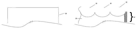
As shown in FIG. 5 e, the support molds 52 are formed in the sacrificial material 26 and may be etched by conventional methods, such as by applying a chemical etching solution followed by a rinse. Preferably, an anisotropic chemical etch is used to etch columnar support molds 52, that correspond to the width and length of the support openings 51 in the surface plane, and that are etched through the sacrificial material 26 to the second micro-lens array 12.
As illustrated in FIG. 5 f, lens molds 29 are also formed in the sacrificial material 26. In a preferred embodiment of the invention, the lens molds 29 may be etched by applying a chemical etching solution followed by a rinse to stop the etching process. Preferably, the chemical etching solution is an isotropic etch solution. An isotropic chemical etch forms a concave lens mold 29 of hemispherical shape.
Referring to FIG. 5 g, supports 20 are formed by filling support molds 52 (shown in FIG. 5 f) with a suitable support material. Suitable support materials are those that are a least substantially non-reflective and that are strong enough to support the upper layers of the image sensor 11 (FIG. 3). In addition, the first micro-lens array 14, including one or more first micro-lenses 15, is formed by coating the sacrificial material 26 (including the lens mold 29 formed therein), thereby filling the lens molds 29, with a first micro-lens material 30, such as for example an SiO2 layer.
In a desired embodiment, both supports 20 and first micro-lens array 14 are comprised of the first micro-lens material 30. In accordance therewith, both the supports 20 and the first micro-lens array 14 are formed by coating the sacrificial material 26 with the first micro-lens material 30. The first micro-lens material 30 fills the support molds 52 to form the supports 20, and also fills the lens molds 29 to form the first micro-lens array 14.
Alternatively, as shown in FIG. 5 h, supports 20 may be comprised of a material other than the first micro-lens material (used to form first micro-lens array 14) that is sufficiently non-reflective and strong. For example if SiO2 is the first micro-lens material, a suitable material for forming the supports 20 may be, for example, silicon nitride. In such case, supports 20 are preferably formed by filling the support molds 52 with the support material before the lens molds 29 are filled with the first micro-lens material 30.
The supports molds 52 may be located at any position such that the supports 20 will be positioned to help support the first layers of the image sensor 11 (including first micro-lens array 14) such as, for example, at edges 21 as shown in FIG. 5 f. Preferably, as shown in FIG. 5 g, the supports 20 are comprised of one or more posts 50 positioned at the edges 21 of the image sensor 11. As shown in FIGS. 5 h and 5 i, posts 50 may be interspersed at the edges 21 along a side plane 54 of the image sensor 11.
In an alternative embodiment of the invention, posts 50 may be positioned internally of edges 21 (as illustrated in FIG. 3 b) at areas within cavity 16 at least substantially outside of the areas wherein incoming light Z is directed from the first micro-lenses 15 to the second micro-lenses 13.
There may be circumstances (due to e.g., equipment limitations) in which it is not feasible to selectively control the application of chemical etching solutions to etch the support molds 52 and the lens molds 29 in a sacrificial material 26 using a sacrificial photo resist having both support openings 51 and sacrificial resist openings 28 developed therein. In such a case, it is desired to form the support openings 51 and to etch the support molds 52 (e.g., using an anisotropic etching solution) prior to forming sacrificial resist openings 28 and etching lens molds 29. After forming support molds 52, a new layer of sacrificial photo resist 27 may be applied to the sacrificial material 26 and sacrificial resist openings 28 developed in the sacrificial photo resist 27, and lens molds 29 etched there through (e.g., using an isotropic etch). The sacrificial photo resist 27 may be stripped, if needed, using known stripping techniques. It should be noted that the sacrificial resist openings 28 and lens molds 29 may alternatively be formed prior to forming the support openings 51 and etching support molds 52.
Additionally, if the support material is not the first micro-lens material 30, there may also be circumstances (such as those due to equipment limitations) in which it is not feasible to selectively control the application of the support material or the first micro-lens material 30 to a sacrificial material 26 having both the support molds 52 and the lens molds 29 formed therein. In such a case, support molds 52 are preferably formed prior to forming lens molds 29. Support molds 52 may then be filled with the support material to form supports 20, as shown in FIG. 5 h. Excess support material may be removed from the sacrificial material using conventional techniques such as by applying chemical solutions and planarization techniques. Lens molds 29 may then be formed and filled with the first micro-lens material 30 to form the first micro-lens array 14 (shown in FIG. 5 h). Alternatively, lens molds 20 may be formed and filled (and excess first micro-lens material 30 removed from the sacrificial material by conventional techniques such as by using chemical solutions or planarization) prior to forming and filling support molds 52.
Referring to FIG. 5 g, sacrificial material 26 is removed to form cavity 16 which provides the embodiment shown in FIG. 3. The sacrificial material 26 may be removed by heat or chemical removal methods such as by heating the sacrificial material 26 or, in the case of a chemical sacrificial material to which a resist has been applied, by treating sacrificial material 26 with solvents or chemicals to remove the resist and sacrificial material 26. As would be known by those of ordinary skill in the art, manufacturers of sacrificial materials may provide recommended removal methods (e.g., heat or chemical) and corresponding process conditions (e.g., temperature or time of removal treatment) for a given sacrificial material.
In a preferred embodiment of the invention, the sacrificial material 26 is removed by heating the sacrificial material to its degradation point. Such heat removal technique may produce a very clean removal such that no additional clean steps are required to remove residual particles.
There may be situations in which a single clean technique (such as heat or chemical removal) does not provide a sufficiently clean image sensor. In such cases, additional clean steps may be desired or required to remove residual sacrificial material or, to remove other residual particles (for example, particles that may remain after a chemical removal). In accordance with an alternative embodiment, additional clean steps, may be provided by the formation and use of vacuum channels 31.
The formation of vacuum channels 31 is now described with reference to FIGS. 6 a through 6 c. Referring to FIG. 6 a, vacuum openings 35 may be formed by applying a vacuum photo resist layer 34 on top of the first micro-lens array 14. The vacuum photo resist layer 34 may be applied by conventional methods, such as for example by spin coating methods.
As shown in FIG. 6 b, the vacuum photo resist layer 34 is exposed, and one or more vacuum openings 35 are developed therein. The vacuum photo resist layer 34 may be exposed by conventional methods such as by masking and developing away desired areas of the photo resist, leaving vacuum openings 35. The vacuum openings 35 should be formed above the non-collimating portions of the first micro-lens array 14. Referring to FIG. 6 c, vacuum channels 31 are formed by etching through the first micro-lens array 14 to the sacrificial material 26. The etching process may be by conventional means, such as by chemical etching. Preferably, the etching process forms vacuum channels 31 of substantially columnar shape. For example, an anisotropic chemical etch may be used to produce substantially columnar shaped vacuum channels 31. After formation of the vacuum channels 31, it is desirable to remove the vacuum photo resist 34 such as by conventional stripping.
The vacuum channels 31 may then be used to remove residual particles that remain after degrading the sacrificial material. The vacuum channels 31 are formed after forming the first micro-lens array, but preferably before cavity 16 is formed by removing sacrificial material 26 (e.g., before degrading the sacrificial material such as by heating or chemical treatment). After the sacrificial material 26 is removed to form cavity 16, it is desirable to plug the vacuum channels 31 by applying a conventional filler material 48, such as a glue, to the outer opening of the vacuum channels 31 as shown in FIG. 6 d.
The vacuum channels 31 alternatively may be located at other areas in the image sensor 11. If the vacuum channels 31 are formed by fabricating a channel or opening through a micro-lens array of the image sensor 11, the vacuum channels 31 should be located in areas that are at least substantially outside of the non-collimating and non-focusing areas of the micro-lens array.
As shown in FIG. 5 i, if the sacrificial material 26 is exposed at areas along one or more side planes 54 of the image sensor 11, then sacrificial material 26 may be removed by vacuuming through one or more exposed areas. Exposed areas of sacrificial material 26 may be formed in a side plane 54 of an image sensor 11, for example, when a series (i.e., multiple) image sensors 11 are fabricated during processing. It is common when fabricating a series of image sensors 11, that a side plane 54 of one image sensor 11 is connected to a side plane 54 of an adjacent image sensor 11 until the final stages of fabrication, at which time each image sensor 11 is separated from the adjacent image sensor 11. As a result of this separation, a side plane 54 of an image sensor 11 may have areas of exposed sacrificial material 26, as shown in FIG. 5 i, through which the sacrificial material 26 may be removed by vacuuming.
The method of fabricating the embodiment of the invention shown in FIG. 4 is now described with reference to FIG. 7 a through FIG. 7 g. As shown in FIG. 7 a, a semiconductor substrate 22 is provided having an M1 layer. As shown in FIG. 7 b, a sacrificial material 26 is applied on top of the M1 layer. It is preferred however, that the color filter array 17 is first provided on top of the M1 layer and then the sacrificial material 26 applied on top of color filter array 17. Examples of suitable sacrificial materials include materials that can be suitably etched and removed from the image sensor, such as for example photosensitive polycarbonates. The sacrificial material 26 may be applied by conventional application methods such as by spin coating the sacrificial material onto the color filter array 17.
As shown in FIG. 7 c, a sacrificial photo resist 27 is applied on top of the sacrificial material 26. The sacrificial photo resist 27 may also be applied by conventional methods such as spin coating.
Referring to FIG. 7 d, the sacrificial photo resist 27 is exposed and areas are developed away to form sacrificial resist openings 28. The sacrificial photo resist 27 may be exposed by conventional methods such as by masking and developing away desired areas of the photo resist, leaving sacrificial resist openings 28.
As also illustrated in FIG. 7 d, the sacrificial photo resist 27 is exposed and areas developed away to form one or more support openings 51. The sacrificial photo resist 27 may be exposed by conventional methods such as by masking and developing away desired areas of the photo resist, leaving support openings 51. Preferably, the support openings 51 are formed in conjunction with the step of forming sacrificial resist openings 28.
Referring to FIG. 7 e, support molds 52 are formed in the sacrificial material 26. The support molds 52 may be etched by conventional methods, such as by applying a chemical etching solution followed by a rinse. Preferably, an anisotropic chemical etch is used to etch columnar support molds, corresponding to the width and length (in the surface plane) of the support openings 51, through the sacrificial material to the adjacent lower level. Preferably this adjacent lower level is the color filter array 17 as shown in FIG. 7 e, but different configurations are also applicable. For example, the adjacent lower level may be the M1 layer.
As illustrated in 7 f, lens molds 29 are formed in the sacrificial material 26. In a preferred embodiment of the invention, lens molds 29 may be etched by applying a chemical etching solution followed by a rinse to stop the etching process. Preferably, the chemical etching solution is an isotropic etch solution (i.e, a solution that etches the sacrificial material 26 at the same rate in all directions). An isotropic chemical etch forms a concave lens molds 29 of hemispherical shape.
Referring to FIG. 7 g, supports 20 are formed by filling support molds 52 (shown in FIG. 7 f) with a suitable support material. Suitable support materials are those that are a least substantially non-reflective and that are strong enough to support the upper layers of the image sensor 11. Supports molds 52 (FIG. 7 f) may be located at any positions such that supports 20 formed thereby are capable of helping to support the first layers of the image sensor 11, including the first micro-lens array 14. As also shown in FIG. 7 g, lens molds 29 (illustrated in FIG. 7 f) are filled with the first micro-lens material 30 to form the first micro-lens array 14.
Preferably, both supports 20 and first micro-lens array 14 are comprised of the first micro-lens material 30. In such case, supports 20 and first micro-lens array 14 may be formed by coating the sacrificial material 26 with the first micro-lens material 30. The first micro-lens material 30 fills the support molds 52 to form the supports 20 and fills the lens molds 29 and to form the first micro-lens array 14. Preferably, the first micro-lens material 30 is SiO2.
Alternatively, supports 20 may be formed separately of the first micro-lens array 14. For example, supports 20 may be formed before the lens molds 29 are filled with the first micro-lens material 30, in which case, supports 20 may be comprised of a material other than the first micro-lens material 30. Suitable materials are those that are at least substantially non-reflective and that have sufficient strength to support the upper layers of the image device 11 including the first micro-lens array 14. Where, for example, the first micro-lens material 30 is SiO2, a different suitable support material such as silicon nitride may be used.
Preferably, as shown in FIG. 7 g, the supports 20 are comprised of one or more posts 50 positioned at the edges 21 of the image sensor 11. If supports 20 are located internally of the edges 21, support molds 52 (shown in FIG. 7 f) should be positioned at locations that are at least substantially outside of the areas through which light is directed from the first micro-lens array 14 to the lower levels of the image sensor 11 (e.g., to the color filter array 17).
In fabricating the embodiment shown in FIG. 4, the sacrificial material 26 (shown in FIG. 7 g) is removed by heat or chemical treatment to form the cavity 16 illustrated in FIG. 4. If additional clean techniques are necessary or desired, vacuum channels 31 may be formed by etching through the first micro-lens array to the sacrificial material as previously described with reference to FIGS. 6 a6 d, or to FIG. 5 i.
The fabrication of the lens molds 29 and support molds 52 of the embodiments shown in FIG. 3 and FIG. 4 has been described by photo resist and etching steps. Another method suitable for fabricating the lens molds 29 and support molds 52 of the FIG. 3 and FIG. 4 embodiments is now described with reference to FIGS. 8 a8 b. According to this method, a sacrificial photo resist and subsequent masking and etching of a sacrificial photo resist are not required. As shown in FIG. 8 a, the sacrificial material 26 is applied to the image sensor (e.g., to the second micro-lens layer when fabricating the embodiment of FIG. 3, or to the color filter array when fabricating the embodiment illustrated in FIG. 4). As shown in FIG. 8 b, the sacrificial material may then be etched using conventional controlled laser etching techniques, such as for example stereo lithography techniques, to form lens molds 29 and support molds 52.
The present invention provides a simple apparatus and method for focusing light on a photo sensor without decreasing the depth of the photo sensor in the semiconductor wafer. Examples of suitable applications include digital imaging applications wherein light is transmitted to a light device of a pixel cell, and in digital image display applications wherein light is transferred from a pixel cell of a display device. The invention is particularly suitable for use in integrated circuit applications using semiconductor devices such as for example CMOS or CCD devices.
The method of forming micro-lens arrays through use of a sacrificial material 26 provides micro-lenses with a desired geometry, and provides a cavity of a desired depth, such that the focal point of the micro-lenses is at a desired point in the substrate (i.e., is at the photo sensors). For example, when using an isotropic etch to form first micro-lenses 15 of a concave shape, the geometry of such micro-lenses may be adjusted by varying the size of the sacrificial resist openings 28 through which the lens molds are etched in the sacrificial material 26, and by controlling the exposure time of the chemical etching solution used to etch said lens molds 29. When using an isotropic etch, the amount of sacrificial material etched in the surface plane of the sacrificial material may be varied by varying the size of the sacrificial resist opening 28. Applying the chemical etching solution to a narrower sacrificial resist opening 28 a will form a lens mold 29 a (shown in FIG. 9 a) that is narrower in the surface plane of the sacrificial material 26, but that is at the same depth perpendicular to the surface plane, relative to a lens mold 29 b (shown in FIG. 9 b) that is formed when the resist solution is applied to a wider sacrificial resist opening 28 b.
The amount of sacrificial material 26 applied during fabrication can be controlled to provide a desired cavity depth, and a desired distance between the first micro-lens array 14 and the lower levels of the image sensor 11 (e.g., the color filter array 17 in the FIG. 4 embodiment or the second micro-lens array 12 in the FIG. 3 embodiment). For example, in a multi-array configuration like that shown in FIG. 3, using more sacrificial material 26 can create a first micro-lens array 14 that is located further away from the second micro-lens array 12 than if less sacrificial material 26 were used. Thus, an image sensor 11 having a desired focal point to which the first micro-lens array 14 and the second micro-lens array 12 direct light within the substrate 22 the micro-lenses can be provided.
Additionally, the depth of the lens molds 29 (and the depth of the cavity 16 that remains after the lens molds 29 are filled and sacrificial material 26 is removed), may be controlled by controlling the exposure time of the etching process.
The lens configurations of the present invention are preferably concave configurations, but can include other lens configurations, such as for example the convex configuration shown in FIG. 10. FIG. 10 is a single array configuration that comprises a first micro-lens array 14 having convex first micro-lenses 15.
Convex first micro-lenses 15 may be formed by controlled laser etching (for example by stereo lithography) of the sacrificial material 26 after it is applied to the image sensor. The embodiment illustrated in FIG. 10 is formed by applying the sacrificial material 26 to the upper layer (e.g., the M1 layer) of a substrate 22 (shown in FIG. 10 a), then forming convex lens molds 29 (such as by controlled laser etching) in the sacrificial material (shown in FIG. 10 b), and forming a convex first micro-lens array 14 by filling the lens molds 29 with first micro-lens material 30 (shown in FIG. 10 c), then removing the sacrificial material 26 to produce the image sensor of FIG. 10.
If multiple micro-lens arrays are desired for the image sensor 11, a second micro-lens array 12 having convex second micro-lenses 13 may be formed prior to applying the sacrificial material 26. Convex micro-lens arrays may be formed by known micro-lens fabrication methods (not illustrated herein). A known method for forming second micro-lenses of convex shape is by applying a lower photo resist 24 to the second micro-lens material 23, then masking and exposing away part of the lower photo resist 24 to develop first openings therein, then heating the second micro-lens material 23 and lower photo resist 24 according to conventional methods such that the surface tension caused by the presence of the undeveloped lower photo resist 24 causes the underlying second micro-lens material 23 to form a second micro-lens array 12 of convex micro-lenses 13. A sacrificial material 26 may be applied to the second micro-lens array 12. Then first micro-lens array 14 and cavity 16 a may then be formed in the manner described with reference to FIGS. 10, and 10 a10 c (except that sacrificial material 26 is applied to the second micro-lens array rather than to the upper layer (e.g., M1 layer) of substrate 22).
FIG. 11 illustrates an exemplary processing system 600 that may utilize the image sensor of the invention. For example, the image sensor 11 of FIG. 3, incorporating first micro-lens array 14 and second micro-lens array 12 constructed in accordance with the embodiment of the invention illustrated in FIGS. 5 a5 i may be part of the processing system 600. Other image sensors may be used in accordance with the present invention, for example, the image sensor 11 of FIG. 4, incorporating first micro-lens array 14 (constructed in accordance with the embodiment of the invention illustrated in FIGS. 7 a7 g) may be used. Any one of the electronic components shown in FIG. 11, including CPU 601 and image sensor 11, may be fabricated as an integrated circuit for use in processing images.
The processing system 600 includes one or more processors 601 coupled to a local bus 604. A memory controller 602 and a primary bus bridge 603 are also coupled to the local bus 604. The processing system 600 may include multiple memory controllers 602 and/or multiple primary bus bridges 603. The memory controller 602 and the primary bus bridge 603 may be integrated as a single device 606.
The memory controller 602 is also coupled to one or more memory buses 607. Each memory bus accepts memory components 608 which include at least one memory device 110. The memory components 608 may be a memory card or a memory module. Examples of memory modules include single inline memory modules (SIMMs) and dual inline memory modules (DIMMs). The memory components 608 may include one or more additional devices 609. For example, in a SIMM or DIMM, the additional device 609 might be a configuration memory, such as a serial presence detect (SPD) memory. The memory controller 602 may also be coupled to a cache memory 605. The cache memory 605 may be the only cache memory in the processing system. Alternatively, other devices, for example, processors 601 may also include cache memories, which may form a cache hierarchy with cache memory 605. If the processing system 600 includes peripherals or controllers which are bus masters or which support direct memory access (DMA), the memory controller 602 may implement a cache coherency protocol. If the memory controller 602 is coupled to a plurality of memory buses 607, each memory bus 607 may be operated in parallel, or different address ranges may be mapped to different memory buses 607.
The primary bus bridge 603 is coupled to at least one peripheral bus 610. Various devices, such as peripherals or additional bus bridges may be coupled to the peripheral bus 610. These devices may include a storage controller 611, a miscellaneous I/O device 614, a secondary bus bridge 615, a multimedia processor 618, and a legacy device interface 620. The primary bus bridge 603 may also be coupled to one or more special purpose high speed ports 622. In a personal computer, for example, the special purpose port might be the Accelerated Graphics Port (AGP), used to couple a high performance video card to the processing system 600.
The storage controller 611 couples one or more storage devices 613, via a storage bus 612, to the peripheral bus 610. For example, the storage controller 611 may be a SCSI controller and storage devices 613 may be SCSI discs. The I/O device 614 may be any sort of peripheral. For example, the I/O device 614 may be a local area network interface, such as an Ethernet card. The secondary bus bridge may be used to interface additional devices via another bus to the processing system. For example, the secondary bus bridge 616 may be a universal serial port (USB) controller used to couple USB devices 617 via to the processing system 600. The multimedia processor 618 may be a sound card, a video capture card, or any other type of media interface, which may also be coupled to one additional device such as speakers 619. The legacy device interface 620 is used to couple legacy devices 621, for example, older styled keyboards and mice, to the processing system 600.
The processing system 600 illustrated in FIG. 11 is only an exemplary processing system with which the invention may be used. While FIG. 11 illustrates a processing architecture especially suitable for a general purpose computer, such as a personal computer or a workstation, it should be recognized that well known modifications can be made to configure the processing system 600 to become more suitable for use in a variety of applications. For example, many electronic devices which require processing may be implemented using a simpler architecture which relies on a CPU 601 coupled to memory components 608 and/or memory devices 110. These electronic devices may include, but are not limited to audio/video processors and recorders, gaming consoles, digital television sets, wired or wireless telephones, navigation devices (including system based on the global positioning system (GPS) and/or inertial navigation), and digital cameras and/or recorders. The imaging devices of the present invention, when coupled to a pixel processor, for example, may be implemented in digital cameras and video processors and recorders. Modifications may include, for example, elimination of unnecessary components, addition of specialized devices or circuits, and/or integration of a plurality of devices.
It should again be noted that although the invention has been described with specific references to CMOS pixel cells having a strained silicon layer, the invention has broader applicability and may be used in any image sensor device. For example, the present invention may be used in conjunction with CCD imagers. Similarly, the processes described above are but only a few methods of many that may be used. The above description and drawings illustrate preferred embodiments which achieve the objects, features, and advantages of the present invention. Although certain advantages and preferred embodiments have been described above, those skilled in the art will recognize that substitutions, additions, deletions, modifications and/or other changes may be made without departing from the spirit or scope of the invention. Accordingly, the invention is not limited by the foregoing description but is only limited by the scope of the appended claims.

Claims (25)

1. A method of fabricating an image sensor, the method comprising:
providing a substrate comprising a plurality of photosensitive regions having photo sensors, and an upper substrate layer;
providing a color filter array on top of the upper substrate layer;
applying a sacrificial material to the upper substrate layer;
forming support molds in the sacrificial material;
forming lens molds in the sacrificial material;
forming supports by filling the support molds with a support material;
forming a first micro-lens array having first micro-lenses by filling the lens molds with a first micro-lens material; and
removing the sacrificial material.
2. The method of claim 1 wherein said step of forming the support molds further comprises:
applying a sacrificial photo resist to the sacrificial material;
applying a mask to the sacrificial photo resist and exposing support openings in the sacrificial photo resist; and
etching the sacrificial material by applying an chemical etching solution to form support molds by etching through the support openings.
3. The method of claim 2 wherein the chemical etching solution is an anisotropic etching solution.
4. The method of claim 1 wherein the step of forming the lens molds further comprises:
applying a sacrificial photo resist to the sacrificial material;
applying a mask to the sacrificial photo resist and exposing sacrificial resist openings in the sacrificial photo resist;
etching the sacrificial material by applying chemical etching solution to form lens molds by etching through the sacrificial resist openings; and
applying a rinse to stop the etching process.
5. The method of claim 4 wherein the chemical etching solution is an isotropic etching solution.
6. The method of claim 1 wherein the step the forming the support molds further comprises etching the support molds in the sacrificial material by controlled laser etching.
7. The method of claim 1 wherein the step the forming the lens molds further comprises etching the lens molds in the sacrificial material by controlled laser etching.
8. The method of claim 1 wherein said sacrificial material degrades upon heating to a degradation point, and the step of removing the sacrificial material comprises heating the sacrificial material to at least the degradation point.
9. The method of claim 1 wherein said removing the sacrificial material comprises treating the sacrificial material with chemical resist solvents.
10. The method of claim 1 wherein the support material is the first micro-lens material.
11. A method of fabricating an image sensor, the method comprising:
providing a substrate comprising a plurality of photosensitive regions having photo sensors, and an upper substrate layer;
applying a sacrificial material above the upper substrate layer;
forming lens molds in the sacrificial material;
forming a micro-lens array having micro-lenses by filling the lens molds with a micro-lens material; and
removing the sacrificial material.
12. The method of claim 11 further comprising:
forming support molds in the sacrificial material; and
forming supports by filling the support molds with a support material.
13. The method of claim 12 wherein said step of forming the support molds further comprises:
applying a sacrificial photo resist to the sacrificial material;
applying a mask to the sacrificial photo resist and exposing support openings in the sacrificial photo resist; and
etching the sacrificial material by applying an chemical etching solution to form support molds by etching through the support openings.
14. The method of claim 13 wherein the chemical etching solution is an anisotropic etching solution.
15. The method of claim 11 wherein the step of forming the lens molds further comprises:
applying a sacrificial photo resist to the sacrificial material;
applying a mask to the sacrificial photo resist and exposing sacrificial resist openings in the sacrificial photo resist;
etching the sacrificial material by applying chemical etching solution to form lens molds by etching through the sacrificial resist openings; and
applying a rinse to stop the etching process.
16. The method of claim 15 wherein the chemical etching solution is an isotropic etching solution.
17. The method of claim 11 wherein the step the forming the lens molds further comprises etching the lens molds in the sacrificial material by controlled laser etching.
18. The method of claim 11 wherein said sacrificial material degrades upon heating to a degradation point, and the step of removing the sacrificial material comprises heating the sacrificial material to at least the degradation point.
19. The method of claim 12 wherein the step of the forming the support molds further comprises etching the support molds in the sacrificial material by controlled laser etching.
20. The method of claim 12 wherein the support material is the micro-lens material.
21. A method of fabricating an image sensor, the method comprising:
providing a substrate comprising a plurality of photosensitive regions having photo sensors, and an upper substrate layer;
providing a color filter array on top of the upper substrate layer;
applying a sacrificial material to the upper substrate layer;
forming support molds in the sacrificial material;
forming lens molds in the sacrificial material;
forming supports by filling the support molds with a support material;
forming a first micro-lens array having first micro-lenses by filling the lens molds with a first micro-lens material;
removing the sacrificial material;
forming vacuum channels through the first micro-lens array, wherein the distal ends of the vacuum channels are adjacent the sacrificial material; and
using the vacuum channels to remove residual particles that remain in the image sensor after the step of removing the sacrificial material.
22. The method of claim 21 wherein the vacuum channels are formed prior to the step of removing the sacrificial material.
23. The method of claim 21 wherein the step of forming vacuum channels further comprises:
applying a vacuum photo resist to the first micro-lens array;
masking the vacuum photo resist and developing vacuum openings therein; and
etching the first micro-lens array through to the sacrificial material with a chemical etching solution.
24. The method of claim 23 wherein the chemical etching solution is an anisotropic etching solution.
25. A method of fabricating an image sensor, the method comprising:
providing a substrate comprising a plurality of photosensitive regions having photo sensors, and an upper substrate layer;
applying a sacrificial material above the upper substrate layer;
forming lens molds in the sacrificial material;
forming a micro-lens array having micro-lenses by filling the lens molds with a micro-lens material;
removing the sacrificial material;
forming support molds in the sacrificial material;
forming supports by filling the support molds with a support material;
forming vacuum channels through the micro-lens array, wherein the distal ends of the vacuum channels are adjacent the sacrificial material; and
using the vacuum channels to remove residual particles that remain in the image sensor after the step of removing the sacrificial material.
US10/667,390 2003-09-23 2003-09-23 Micro-lens configuration for small lens focusing in digital imaging devices Expired - Lifetime US7115853B2 (en)

Priority Applications (3)

Application Number Priority Date Filing Date Title
US10/667,390 US7115853B2 (en) 2003-09-23 2003-09-23 Micro-lens configuration for small lens focusing in digital imaging devices
US11/257,039 US7405385B2 (en) 2003-09-23 2005-10-25 Micro-lens configuration for small lens focusing in digital imaging devices
US11/257,041 US7557337B2 (en) 2003-09-23 2005-10-25 Micro-lens configuration for small lens focusing in digital imaging devices

Applications Claiming Priority (1)

Application Number Priority Date Filing Date Title
US10/667,390 US7115853B2 (en) 2003-09-23 2003-09-23 Micro-lens configuration for small lens focusing in digital imaging devices

Related Child Applications (2)

Application Number Title Priority Date Filing Date
US11/257,041 Division US7557337B2 (en) 2003-09-23 2005-10-25 Micro-lens configuration for small lens focusing in digital imaging devices
US11/257,039 Division US7405385B2 (en) 2003-09-23 2005-10-25 Micro-lens configuration for small lens focusing in digital imaging devices

Publications (2)

Publication Number Publication Date
US20050061950A1 US20050061950A1 (en) 2005-03-24
US7115853B2 true US7115853B2 (en) 2006-10-03

Family

ID=34313287

Family Applications (3)

Application Number Title Priority Date Filing Date
US10/667,390 Expired - Lifetime US7115853B2 (en) 2003-09-23 2003-09-23 Micro-lens configuration for small lens focusing in digital imaging devices
US11/257,041 Expired - Lifetime US7557337B2 (en) 2003-09-23 2005-10-25 Micro-lens configuration for small lens focusing in digital imaging devices
US11/257,039 Active 2024-08-24 US7405385B2 (en) 2003-09-23 2005-10-25 Micro-lens configuration for small lens focusing in digital imaging devices

Family Applications After (2)

Application Number Title Priority Date Filing Date
US11/257,041 Expired - Lifetime US7557337B2 (en) 2003-09-23 2005-10-25 Micro-lens configuration for small lens focusing in digital imaging devices
US11/257,039 Active 2024-08-24 US7405385B2 (en) 2003-09-23 2005-10-25 Micro-lens configuration for small lens focusing in digital imaging devices

Country Status (1)

Country Link
US (3) US7115853B2 (en)

Cited By (23)

* Cited by examiner, † Cited by third party
Publication number Priority date Publication date Assignee Title
US20050275741A1 (en) * 2004-06-15 2005-12-15 Fujitsu Limited Image pickup device and production method thereof
US20060039044A1 (en) * 2004-08-20 2006-02-23 Dongbuanam Semiconductor Inc. Self-aligned image sensor and method for fabricating the same
US20060097295A1 (en) * 2004-11-09 2006-05-11 Donganam Semiconductor Inc. CMOS image sensor and method for fabricating the same
US20060128051A1 (en) * 2004-12-14 2006-06-15 Kim Yeong S Method of fabricating CMOS image sensor
US20060236721A1 (en) * 2005-04-20 2006-10-26 United States Of America As Represented By The Dept Of The Army Method of manufacture for a compound eye
US20070002159A1 (en) * 2005-07-01 2007-01-04 Olsen Richard I Method and apparatus for use in camera and systems employing same
US20070019306A1 (en) * 2001-04-10 2007-01-25 President And Fellows Of Harvard College Microlens for projection lithography and method of preparation thereof
US20070211164A1 (en) * 2004-08-25 2007-09-13 Olsen Richard I Imager module optical focus and assembly method
US20070257184A1 (en) * 2005-08-25 2007-11-08 Olsen Richard I Large dynamic range cameras
US20070258006A1 (en) * 2005-08-25 2007-11-08 Olsen Richard I Solid state camera optics frame and assembly
US20070296835A1 (en) * 2005-08-25 2007-12-27 Olsen Richard I Digital cameras with direct luminance and chrominance detection
US20070295893A1 (en) * 2004-08-25 2007-12-27 Olsen Richard I Lens frame and optical focus assembly for imager module
US20080023734A1 (en) * 2006-07-31 2008-01-31 Eun-Sang Cho Microlenses of cmos image sensor and method for fabricating the same
US20080030597A1 (en) * 2004-08-25 2008-02-07 Newport Imaging Corporation Digital camera with multiple pipeline signal processors
US20080029714A1 (en) * 2005-08-25 2008-02-07 Newport Imaging Corporation Digital camera with integrated infrared (IR) response
US20080174670A1 (en) * 2004-08-25 2008-07-24 Richard Ian Olsen Simultaneous multiple field of view digital cameras
US20080278820A1 (en) * 2007-05-08 2008-11-13 Micron Technology, Inc. Tetraform microlenses and method of forming the same
US20080290435A1 (en) * 2007-05-21 2008-11-27 Micron Technology, Inc. Wafer level lens arrays for image sensor packages and the like, image sensor packages, and related methods
US20090224343A1 (en) * 2008-03-06 2009-09-10 Micron Technology, Inc. Methods of forming imager devices, imager devices configured for back side illumination, and systems including the same
US20090256228A1 (en) * 2003-11-26 2009-10-15 Boettiger Ulrich C Micro-lenses for cmos imagers and method for manufacturing micro-lenses
US20090315201A1 (en) * 2003-11-17 2009-12-24 Jin Li Method of forming micro-lenses
US20110059341A1 (en) * 2008-06-12 2011-03-10 Junichi Matsumoto Electric vehicle
US8704935B2 (en) 2011-01-25 2014-04-22 Aptina Imaging Corporation Imaging systems with arrays of aligned lenses

Families Citing this family (33)

* Cited by examiner, † Cited by third party
Publication number Priority date Publication date Assignee Title
US7511749B2 (en) * 2003-12-18 2009-03-31 Aptina Imaging Corporation Color image sensor having imaging element array forming images on respective regions of sensor elements
US7851837B2 (en) * 2003-12-18 2010-12-14 Panasonic Corporation Light-collecting device and solid-state imaging apparatus
US7425933B2 (en) * 2004-04-14 2008-09-16 Samsung Semiconductor Israel R&D Center (Sirc) Systems and methods for correcting green disparity in imager sensors
JP4830306B2 (en) * 2004-06-23 2011-12-07 凸版印刷株式会社 Manufacturing method of solid-state imaging device
KR100649019B1 (en) * 2004-08-11 2006-11-24 동부일렉트로닉스 주식회사 CMOS Image sensor and Method for fabricating of the same
US7329856B2 (en) * 2004-08-24 2008-02-12 Micron Technology, Inc. Image sensor having integrated infrared-filtering optical device and related method
EP1785750A1 (en) * 2004-09-01 2007-05-16 Matsushita Electric Industrial Co., Ltd. Condensing element, solid-state imaging device and method for fabricating the same
JP4822683B2 (en) * 2004-10-08 2011-11-24 パナソニック株式会社 Solid-state imaging device and manufacturing method thereof
US7829965B2 (en) * 2005-05-18 2010-11-09 International Business Machines Corporation Touching microlens structure for a pixel sensor and method of fabrication
US7553689B2 (en) * 2005-07-13 2009-06-30 Taiwan Semiconductor Manufacturing Co., Ltd. Semiconductor device with micro-lens and method of making the same
JP4561726B2 (en) * 2006-01-18 2010-10-13 セイコーエプソン株式会社 Manufacturing method of member with recess and manufacturing method of lens substrate
KR101255275B1 (en) 2006-10-13 2013-04-15 엘지디스플레이 주식회사 Steroscopic Liquid Crystal Display Device, method for Manufacturing the same and Bonding Apparatus for the same
US20080142685A1 (en) * 2006-12-13 2008-06-19 Gazeley William G Integrated image sensor having a color-filtering microlens, and related system and method
US9153614B2 (en) * 2007-08-15 2015-10-06 Micron Technology, Inc. Method and apparatus for lens alignment for optically sensitive devices and systems implementing same
US20090101947A1 (en) * 2007-10-17 2009-04-23 Visera Technologies Company Limited Image sensor device and fabrication method thereof
US8003425B2 (en) * 2008-05-14 2011-08-23 International Business Machines Corporation Methods for forming anti-reflection structures for CMOS image sensors
US7759755B2 (en) 2008-05-14 2010-07-20 International Business Machines Corporation Anti-reflection structures for CMOS image sensors
US8129764B2 (en) 2008-06-11 2012-03-06 Aptina Imaging Corporation Imager devices having differing gate stack sidewall spacers, method for forming such imager devices, and systems including such imager devices
US8450821B2 (en) * 2009-03-26 2013-05-28 Micron Technology, Inc. Method and apparatus providing combined spacer and optical lens element
WO2010139343A1 (en) 2009-06-02 2010-12-09 Fraunhofer-Gesellschaft zur Förderung der angewandten Forschung e.V. Lens and method for manufacturing same
WO2010139342A1 (en) * 2009-06-02 2010-12-09 Fraunhofer-Gesellschaft zur Förderung der angewandten Forschung e. V. Lens and method for manufacturing same
US20100321640A1 (en) * 2009-06-22 2010-12-23 Industrial Technology Research Institute Projection display chip
CN102130138B (en) * 2010-01-12 2013-01-02 中芯国际集成电路制造(上海)有限公司 Image sensor and forming method thereof
US10190960B2 (en) 2013-03-14 2019-01-29 Cytonome/St, Llc Micro-lens systems for particle processing systems
US9547231B2 (en) * 2013-06-12 2017-01-17 Avago Technologies General Ip (Singapore) Pte. Ltd. Device and method for making photomask assembly and photodetector device having light-collecting optical microstructure
US10115757B2 (en) * 2014-08-22 2018-10-30 SK Hynix Inc. Image sensor and electronic device having the same
JP6519355B2 (en) * 2015-06-30 2019-05-29 株式会社デンソー Camera apparatus and in-vehicle system
US10304811B2 (en) * 2015-09-04 2019-05-28 Hong Kong Beida Jade Bird Display Limited Light-emitting diode display panel with micro lens array
US9977152B2 (en) * 2016-02-24 2018-05-22 Hong Kong Beida Jade Bird Display Limited Display panels with integrated micro lens array
US10304375B2 (en) 2016-09-23 2019-05-28 Hong Kong Beida Jade Bird Display Limited Micro display panels with integrated micro-reflectors
DE102017218772A1 (en) * 2017-10-20 2019-04-25 Infineon Technologies Dresden Gmbh Microlens with a strapless optical interference filter
JP7305310B2 (en) * 2018-05-25 2023-07-10 デクセリアルズ株式会社 Optical unit, light irradiation device, image display device, and method for manufacturing optical unit
US20210140764A1 (en) * 2019-11-07 2021-05-13 Spectricity Collimating array for an optical sensing device

Citations (7)

* Cited by examiner, † Cited by third party
Publication number Priority date Publication date Assignee Title
US5672519A (en) 1994-02-23 1997-09-30 Lg Semicon Co., Ltd. Method of fabricating solid state image sensing elements
US5877040A (en) * 1995-08-10 1999-03-02 Lg Semicon Co., Ltd. Method of making charge-coupled device with microlens
US5976907A (en) * 1995-05-02 1999-11-02 Matsushita Electronics Corporation Solid state imaging device and production method for the same
US6030852A (en) * 1995-05-22 2000-02-29 Matsushita Electronics Corporation Solid-state imaging device and method of manufacturing the same
US6066511A (en) * 1995-08-23 2000-05-23 Sony Corporation Manufacturing method for a solid state imaging device
US6381072B1 (en) * 1998-01-23 2002-04-30 Proxemics Lenslet array systems and methods
US20030168679A1 (en) * 2002-02-05 2003-09-11 Junichi Nakai Semiconductor device and method of manufacturing the same

Family Cites Families (13)

* Cited by examiner, † Cited by third party
Publication number Priority date Publication date Assignee Title
JP2833941B2 (en) * 1992-10-09 1998-12-09 三菱電機株式会社 Solid-state imaging device and method of manufacturing the same
JP2821421B2 (en) * 1996-05-21 1998-11-05 日本電気株式会社 Solid-state imaging device
GB9618717D0 (en) * 1996-09-07 1996-10-16 Philips Electronics Nv Image sensor
JP3447510B2 (en) * 1997-04-09 2003-09-16 Necエレクトロニクス株式会社 Solid-state imaging device, manufacturing method thereof, and solid-state imaging device
JP3938253B2 (en) * 1997-12-26 2007-06-27 日本板硝子株式会社 Resin erecting equal-magnification lens array and manufacturing method thereof
KR100310102B1 (en) * 1998-03-05 2001-12-17 윤종용 Solid-state color imaging device and method for fabricating the same
JP3571909B2 (en) * 1998-03-19 2004-09-29 キヤノン株式会社 Solid-state imaging device and method of manufacturing the same
JPH11284158A (en) * 1998-03-27 1999-10-15 Sony Corp Solid image pick-up element and manufacture of solid image pick-up element
JP4232213B2 (en) * 1998-04-15 2009-03-04 ソニー株式会社 Solid-state image sensor
WO2000045199A1 (en) * 1999-01-29 2000-08-03 Rohm Co., Ltd. Lens unit for image formation, and image reader having lens unit
US6171885B1 (en) * 1999-10-12 2001-01-09 Taiwan Semiconductor Manufacturing Company High efficiency color filter process for semiconductor array imaging devices
US6646807B2 (en) * 2001-06-19 2003-11-11 Rohm Co., Ltd. Lens array unit and process for making lens array
US6624444B1 (en) * 2002-03-28 2003-09-23 Intel Corporation Electrical-optical package with capacitor DC shunts and associated methods

Patent Citations (7)

* Cited by examiner, † Cited by third party
Publication number Priority date Publication date Assignee Title
US5672519A (en) 1994-02-23 1997-09-30 Lg Semicon Co., Ltd. Method of fabricating solid state image sensing elements
US5976907A (en) * 1995-05-02 1999-11-02 Matsushita Electronics Corporation Solid state imaging device and production method for the same
US6030852A (en) * 1995-05-22 2000-02-29 Matsushita Electronics Corporation Solid-state imaging device and method of manufacturing the same
US5877040A (en) * 1995-08-10 1999-03-02 Lg Semicon Co., Ltd. Method of making charge-coupled device with microlens
US6066511A (en) * 1995-08-23 2000-05-23 Sony Corporation Manufacturing method for a solid state imaging device
US6381072B1 (en) * 1998-01-23 2002-04-30 Proxemics Lenslet array systems and methods
US20030168679A1 (en) * 2002-02-05 2003-09-11 Junichi Nakai Semiconductor device and method of manufacturing the same

Non-Patent Citations (3)

* Cited by examiner, † Cited by third party
Title
Air-Channel Fabrication for Microelectromechanical Systems Via Sacrificial Photosensitive Polycarbonates, Joseph Paul Jayachandran, Hollie A. Reed, Hongshi Zhen, Larry F. Rhodes, Clifford L. Henderson, Sue Ann Bidstrup Allen, and Paul A. Kohl, School of Chemical Engineering, Georgia Institute of Technology, Atlanta, GA (b) Promerus LLC, Brecksville, OH.
Fabrication of Air-Channel Structures for Microfluidic, Microelectromechanical, and Microelectronic Applications, Dhananjay Bhusari, Hollie A. Reed, Michael Wedlake, Agnes M. Padovani, Sue Ann Bidstrup Allen, and Paul A. Kohl, Member, IEEE, Journal of Microelectromechanical System, vol. 10, No. 3, Sep. 2001.
Fabrication of microchannels using polycarbonates as sacrificial materials, Hollie A. Reed, Celesta E. White, Vikram Rao, Sue Ann Bidstrup Allen, Clifford L. Henderson and Paul A. Kohl, School of Chemical Engineering, Georgia Institute of Technology, Atlanta, GA, Oct. 12, 2001, Journal of Micromechanics and Microengineering, Institute of Physics Publishing, J. Micromech, Microeng. 11 (2001) 733-737.

Cited By (66)

* Cited by examiner, † Cited by third party
Publication number Priority date Publication date Assignee Title
US7403338B2 (en) 2001-04-10 2008-07-22 President & Fellows Of Harvard College Microlens for projection lithography and method of preparation thereof
US20070019306A1 (en) * 2001-04-10 2007-01-25 President And Fellows Of Harvard College Microlens for projection lithography and method of preparation thereof
US8361332B2 (en) 2003-11-17 2013-01-29 Micron Technology, Inc. Method of forming micro-lenses
US20090315201A1 (en) * 2003-11-17 2009-12-24 Jin Li Method of forming micro-lenses
US8390931B2 (en) 2003-11-26 2013-03-05 Aptina Imaging Corporation Micro-lenses for CMOS imagers and method for manufacturing micro-lenses
US20090256228A1 (en) * 2003-11-26 2009-10-15 Boettiger Ulrich C Micro-lenses for cmos imagers and method for manufacturing micro-lenses
US8411197B2 (en) * 2004-06-15 2013-04-02 Fujitsu Semiconductor Limited Image pickup device and production method thereof
US20050275741A1 (en) * 2004-06-15 2005-12-15 Fujitsu Limited Image pickup device and production method thereof
US20060039044A1 (en) * 2004-08-20 2006-02-23 Dongbuanam Semiconductor Inc. Self-aligned image sensor and method for fabricating the same
US20080174670A1 (en) * 2004-08-25 2008-07-24 Richard Ian Olsen Simultaneous multiple field of view digital cameras
US8415605B2 (en) 2004-08-25 2013-04-09 Protarius Filo Ag, L.L.C. Digital camera with multiple pipeline signal processors
US20070295893A1 (en) * 2004-08-25 2007-12-27 Olsen Richard I Lens frame and optical focus assembly for imager module
US10142548B2 (en) 2004-08-25 2018-11-27 Callahan Cellular L.L.C. Digital camera with multiple pipeline signal processors
US20080030597A1 (en) * 2004-08-25 2008-02-07 Newport Imaging Corporation Digital camera with multiple pipeline signal processors
US8198574B2 (en) 2004-08-25 2012-06-12 Protarius Filo Ag, L.L.C. Large dynamic range cameras
US10009556B2 (en) 2004-08-25 2018-06-26 Callahan Cellular L.L.C. Large dynamic range cameras
US9313393B2 (en) 2004-08-25 2016-04-12 Callahan Cellular L.L.C. Digital camera with multiple pipeline signal processors
US9232158B2 (en) 2004-08-25 2016-01-05 Callahan Cellular L.L.C. Large dynamic range cameras
US8334494B2 (en) 2004-08-25 2012-12-18 Protarius Filo Ag, L.L.C. Large dynamic range cameras
US7916180B2 (en) 2004-08-25 2011-03-29 Protarius Filo Ag, L.L.C. Simultaneous multiple field of view digital cameras
US8664579B2 (en) 2004-08-25 2014-03-04 Protarius Filo Ag, L.L.C. Digital camera with multiple pipeline signal processors
US8598504B2 (en) 2004-08-25 2013-12-03 Protarius Filo Ag, L.L.C. Large dynamic range cameras
US7884309B2 (en) 2004-08-25 2011-02-08 Richard Ian Olsen Digital camera with multiple pipeline signal processors
US8436286B2 (en) 2004-08-25 2013-05-07 Protarius Filo Ag, L.L.C. Imager module optical focus and assembly method
US8124929B2 (en) 2004-08-25 2012-02-28 Protarius Filo Ag, L.L.C. Imager module optical focus and assembly method
US7795577B2 (en) 2004-08-25 2010-09-14 Richard Ian Olsen Lens frame and optical focus assembly for imager module
US20070211164A1 (en) * 2004-08-25 2007-09-13 Olsen Richard I Imager module optical focus and assembly method
US20090268043A1 (en) * 2004-08-25 2009-10-29 Richard Ian Olsen Large dynamic range cameras
US20090302205A9 (en) * 2004-08-25 2009-12-10 Olsen Richard I Lens frame and optical focus assembly for imager module
US20100208100A9 (en) * 2004-08-25 2010-08-19 Newport Imaging Corporation Digital camera with multiple pipeline signal processors
US20100060746A9 (en) * 2004-08-25 2010-03-11 Richard Ian Olsen Simultaneous multiple field of view digital cameras
US20060097295A1 (en) * 2004-11-09 2006-05-11 Donganam Semiconductor Inc. CMOS image sensor and method for fabricating the same
US7538374B2 (en) * 2004-11-09 2009-05-26 Dongbu Electronics Co., Inc. CMOS image sensor and method for fabricating the same
US20060128051A1 (en) * 2004-12-14 2006-06-15 Kim Yeong S Method of fabricating CMOS image sensor
US20080237671A1 (en) * 2004-12-14 2008-10-02 Yeong Sil Kim Method of Fabricating CMOS Image Sensor
US7416914B2 (en) 2004-12-14 2008-08-26 Dongbu Electronics Co., Ltd. Method of fabricating CMOS image sensor
US20060236721A1 (en) * 2005-04-20 2006-10-26 United States Of America As Represented By The Dept Of The Army Method of manufacture for a compound eye
US7714262B2 (en) 2005-07-01 2010-05-11 Richard Ian Olsen Digital camera with integrated ultraviolet (UV) response
US7772532B2 (en) 2005-07-01 2010-08-10 Richard Ian Olsen Camera and method having optics and photo detectors which are adjustable with respect to each other
US20070002159A1 (en) * 2005-07-01 2007-01-04 Olsen Richard I Method and apparatus for use in camera and systems employing same
US20080029708A1 (en) * 2005-07-01 2008-02-07 Newport Imaging Corporation Digital camera with integrated ultraviolet (UV) response
US7566855B2 (en) 2005-08-25 2009-07-28 Richard Ian Olsen Digital camera with integrated infrared (IR) response
US11412196B2 (en) 2005-08-25 2022-08-09 Intellectual Ventures Ii Llc Digital cameras with direct luminance and chrominance detection
US20110205407A1 (en) * 2005-08-25 2011-08-25 Richard Ian Olsen Digital cameras with direct luminance and chrominance detection
US11706535B2 (en) 2005-08-25 2023-07-18 Intellectual Ventures Ii Llc Digital cameras with direct luminance and chrominance detection
US8304709B2 (en) 2005-08-25 2012-11-06 Protarius Filo Ag, L.L.C. Digital cameras with direct luminance and chrominance detection
US7964835B2 (en) 2005-08-25 2011-06-21 Protarius Filo Ag, L.L.C. Digital cameras with direct luminance and chrominance detection
US11425349B2 (en) 2005-08-25 2022-08-23 Intellectual Ventures Ii Llc Digital cameras with direct luminance and chrominance detection
US9294745B2 (en) 2005-08-25 2016-03-22 Callahan Cellular L.L.C. Digital cameras with direct luminance and chrominance detection
US10694162B2 (en) 2005-08-25 2020-06-23 Callahan Cellular L.L.C. Digital cameras with direct luminance and chrominance detection
US20070296835A1 (en) * 2005-08-25 2007-12-27 Olsen Richard I Digital cameras with direct luminance and chrominance detection
US7564019B2 (en) 2005-08-25 2009-07-21 Richard Ian Olsen Large dynamic range cameras
US10148927B2 (en) 2005-08-25 2018-12-04 Callahan Cellular L.L.C. Digital cameras with direct luminance and chrominance detection
US8629390B2 (en) 2005-08-25 2014-01-14 Protarius Filo Ag, L.L.C. Digital cameras with direct luminance and chrominance detection
US20080029714A1 (en) * 2005-08-25 2008-02-07 Newport Imaging Corporation Digital camera with integrated infrared (IR) response
US20070258006A1 (en) * 2005-08-25 2007-11-08 Olsen Richard I Solid state camera optics frame and assembly
US20070257184A1 (en) * 2005-08-25 2007-11-08 Olsen Richard I Large dynamic range cameras
US20080023734A1 (en) * 2006-07-31 2008-01-31 Eun-Sang Cho Microlenses of cmos image sensor and method for fabricating the same
US7638348B2 (en) * 2006-07-31 2009-12-29 Dongbu Hitek Co., Ltd. Microlenses of CMOS image sensor and method for fabricating the same
US20080278820A1 (en) * 2007-05-08 2008-11-13 Micron Technology, Inc. Tetraform microlenses and method of forming the same
US20110234883A1 (en) * 2007-05-08 2011-09-29 Jin Li Tetraform microlenses and method of forming the same
US7978411B2 (en) 2007-05-08 2011-07-12 Micron Technology, Inc. Tetraform microlenses and method of forming the same
US20080290435A1 (en) * 2007-05-21 2008-11-27 Micron Technology, Inc. Wafer level lens arrays for image sensor packages and the like, image sensor packages, and related methods
US20090224343A1 (en) * 2008-03-06 2009-09-10 Micron Technology, Inc. Methods of forming imager devices, imager devices configured for back side illumination, and systems including the same
US20110059341A1 (en) * 2008-06-12 2011-03-10 Junichi Matsumoto Electric vehicle
US8704935B2 (en) 2011-01-25 2014-04-22 Aptina Imaging Corporation Imaging systems with arrays of aligned lenses

Also Published As

Publication number Publication date
US20060033010A1 (en) 2006-02-16
US20050061950A1 (en) 2005-03-24
US7405385B2 (en) 2008-07-29
US20060038112A1 (en) 2006-02-23
US7557337B2 (en) 2009-07-07

Similar Documents

Publication Publication Date Title
US7115853B2 (en) Micro-lens configuration for small lens focusing in digital imaging devices
US11843015B2 (en) Image sensors
US7683407B2 (en) Structure and method for building a light tunnel for use with imaging devices
US6995442B2 (en) Total internal reflection (TIR) CMOS imager
CN102034842B (en) Solid-state imaging device, solid-state imaging device manufacturing method, electronic device, and lens array
US20070014019A1 (en) Sharing of microlenses among pixels in image sensors
US20090160983A1 (en) Method and apparatus providing light traps for optical crosstalk reduction
US20060267121A1 (en) Microlenses for imaging devices
EP1705706B1 (en) Solid-state imaging device
KR100504563B1 (en) Method for fabricating an image sensor
US10804306B2 (en) Solid-state imaging devices having flat microlenses
TWI389330B (en) Backside illuminated imager and method of fabricating the same
CN101404289B (en) Image sensor and method of fabricating the same
CN102637707B (en) Method of producing semiconductor device and method of producing solid-state image pickup device
US20090224343A1 (en) Methods of forming imager devices, imager devices configured for back side illumination, and systems including the same
KR20010061308A (en) Method for fabricating thin film image sensor
KR100906558B1 (en) Image Sensor and Method for Manufacturing Thereof
KR100788375B1 (en) Method of manufacturing image sensor
US7972891B2 (en) Image sensor and method for manufacturing the same
KR100741920B1 (en) method for fabricating CMOS image sensor
KR100729744B1 (en) Method of manufacturing cmos image sensor
KR20030039712A (en) Image sensor and method of fabricating the same
KR20030039713A (en) Image sensor and method of fabricating the same
KR100959442B1 (en) Image Sensor and Method for Manufacturing Thereof
TWI308226B (en) Microlens structure and fabricating method thereof

Legal Events

Date Code Title Description
AS Assignment

Owner name: MICRON TECHNOLOGY, INC., IDAHO

Free format text: ASSIGNMENT OF ASSIGNORS INTEREST;ASSIGNORS:JIANG, TONGBI;CONNELL, MICHAEL;LI, JIN;REEL/FRAME:014536/0335

Effective date: 20030902

STCF Information on status: patent grant

Free format text: PATENTED CASE

CC Certificate of correction
FEPP Fee payment procedure

Free format text: PAYOR NUMBER ASSIGNED (ORIGINAL EVENT CODE: ASPN); ENTITY STATUS OF PATENT OWNER: LARGE ENTITY

AS Assignment

Owner name: APTINA IMAGING CORPORATION, CAYMAN ISLANDS

Free format text: ASSIGNMENT OF ASSIGNORS INTEREST;ASSIGNOR:MICRON TECHNOLOGY, INC.;REEL/FRAME:022368/0501

Effective date: 20080926

FPAY Fee payment

Year of fee payment: 4

FPAY Fee payment

Year of fee payment: 8

MAFP Maintenance fee payment

Free format text: PAYMENT OF MAINTENANCE FEE, 12TH YEAR, LARGE ENTITY (ORIGINAL EVENT CODE: M1553)

Year of fee payment: 12