US6853129B1 - Protected substrate structure for a field emission display device - Google Patents
Protected substrate structure for a field emission display device Download PDFInfo
- Publication number
- US6853129B1 US6853129B1 US10/412,196 US41219603A US6853129B1 US 6853129 B1 US6853129 B1 US 6853129B1 US 41219603 A US41219603 A US 41219603A US 6853129 B1 US6853129 B1 US 6853129B1
- Authority
- US
- United States
- Prior art keywords
- present
- faceplate
- display device
- field emission
- emission display
- Prior art date
- Legal status (The legal status is an assumption and is not a legal conclusion. Google has not performed a legal analysis and makes no representation as to the accuracy of the status listed.)
- Expired - Fee Related
Links
Images


Classifications
-
- H—ELECTRICITY
- H01—ELECTRIC ELEMENTS
- H01J—ELECTRIC DISCHARGE TUBES OR DISCHARGE LAMPS
- H01J1/00—Details of electrodes, of magnetic control means, of screens, or of the mounting or spacing thereof, common to two or more basic types of discharge tubes or lamps
- H01J1/02—Main electrodes
- H01J1/30—Cold cathodes, e.g. field-emissive cathode
- H01J1/304—Field-emissive cathodes
-
- H—ELECTRICITY
- H01—ELECTRIC ELEMENTS
- H01J—ELECTRIC DISCHARGE TUBES OR DISCHARGE LAMPS
- H01J29/00—Details of cathode-ray tubes or of electron-beam tubes of the types covered by group H01J31/00
- H01J29/02—Electrodes; Screens; Mounting, supporting, spacing or insulating thereof
- H01J29/06—Screens for shielding; Masks interposed in the electron stream
-
- H—ELECTRICITY
- H01—ELECTRIC ELEMENTS
- H01J—ELECTRIC DISCHARGE TUBES OR DISCHARGE LAMPS
- H01J29/00—Details of cathode-ray tubes or of electron-beam tubes of the types covered by group H01J31/00
- H01J29/02—Electrodes; Screens; Mounting, supporting, spacing or insulating thereof
- H01J29/08—Electrodes intimately associated with a screen on or from which an image or pattern is formed, picked-up, converted or stored, e.g. backing-plates for storage tubes or collecting secondary electrons
- H01J29/085—Anode plates, e.g. for screens of flat panel displays
-
- H—ELECTRICITY
- H01—ELECTRIC ELEMENTS
- H01J—ELECTRIC DISCHARGE TUBES OR DISCHARGE LAMPS
- H01J2201/00—Electrodes common to discharge tubes
- H01J2201/02—Arrangements for eliminating deleterious effects
-
- H—ELECTRICITY
- H01—ELECTRIC ELEMENTS
- H01J—ELECTRIC DISCHARGE TUBES OR DISCHARGE LAMPS
- H01J2211/00—Plasma display panels with alternate current induction of the discharge, e.g. AC-PDPs
- H01J2211/20—Constructional details
- H01J2211/34—Vessels, containers or parts thereof, e.g. substrates
- H01J2211/36—Spacers, barriers, ribs, partitions or the like
-
- H—ELECTRICITY
- H01—ELECTRIC ELEMENTS
- H01J—ELECTRIC DISCHARGE TUBES OR DISCHARGE LAMPS
- H01J2329/00—Electron emission display panels, e.g. field emission display panels
Definitions
- the present claimed invention relates to the field of flat panel displays. More particularly, the present claimed invention relates to the “black matrix” of a flat panel display screen structure.
- Sub-pixel regions on the faceplate of a flat panel display are typically separated by an opaque mesh-like structure commonly referred to as a matrix or “black matrix”.
- black matrix By separating sub-pixel regions, the black matrix prevents electrons directed at one sub-pixel from being overlapping another sub-pixel. In so doing, a conventional black matrix helps maintain color purity in a flat panel display.
- the black matrix is also used as a base on which to locate structures such as, for example, support walls.
- the black matrix is three dimensional (i.e. it extends above the level of the light emitting phosphors), then the black matrix can prevent some of the electrons back scattered from the phosphors of one sub-pixel from impinging on another, thereby improving color purity.
- Polyimide material may be used to form the matrix. It is known that polyimide material contains numerous components such as nitrogen, hydrogen, carbon, and oxygen. While contained within the polyimide material, these aforementioned constituents do not negatively affect the vacuum environment of the flat panel display. Unfortunately, conventional polyimide matrices and the constituents thereof do not always remain confined within the polyimide material. That is, under certain conditions, the polyimide constituents, and combinations thereof, are released from the polyimide material of the matrix. As a result, the vacuum environment of the flat panel display is compromised.
- Polyimide (or other black matrix material) constituent contamination occurs in various ways.
- thermally treating or heating a conventional polyimide matrix can cause low molecular weight components (fragments, monomers or groups of monomers) of the polyimide material to migrate to the surface of the matrix. These low molecular weight components can then move out of the matrix and onto the faceplate. When energetic electrons strike the contaminant-coated faceplate, polymerization of the contaminants can occur. This polymerization, in turn, results in the formation of a dark coating on the faceplate. The dark coating reduces brightness of the display thereby degrading overall performance of the flat panel display.
- conventional polyimide matrices In addition to thermally induced contamination, conventional polyimide matrices also suffer from electron stimulated desorption of contaminants. That is, during operation, a cathode portion of the flat panel display emits electrons which are directed towards sub-pixel regions on the faceplate. However, some of these emitted electrons will eventually strike the matrix. This electron bombardment of the conventional polyimide matrix results in electron-stimulated desorption of contaminants (i.e. constituents or decomposition products of the polyimide matrix). These emitted contaminants arising from the polyimide matrix are then deleteriously introduced into the vacuum environment of the flat panel display. The contaminants emitted into the vacuum environment degrade the vacuum, can induce sputtering, and may also coat the surface of the field emitters.
- contaminants i.e. constituents or decomposition products of the polyimide matrix
- conventional polyimide matrices also suffer from X-ray stimulated desorption of contaminants. That is, during operation, X-rays (i.e. high energy photons) are generated by, for example, electrons striking the phosphors. Some of these generated X-rays will eventually strike the matrix. Such X-ray bombardment of the conventional polyimide matrix results in X-ray stimulated desorption of contaminants (i.e. constituents or decomposition products of the polyimide matrix). As described above, these emitted contaminants arising from the polyimide matrix are then deleteriously introduced into the vacuum environment of the flat panel display. Like electron stimulated contaminants, these constituents degrade the vacuum, can induce sputtering, and may also coat the surface of the field emitters.
- X-rays i.e. high energy photons
- contaminants i.e. constituents or decomposition products of the polyimide matrix
- the faceplate of a field emission cathode ray tube requires a conductive anode electrode to carry the current used to illuminate the display.
- a conductive black matrix structure also provides a uniform potential surface, reducing the likelihood of electrical arcing.
- conventional polyimide matrices are not conductive. Therefore, local charging of the black matrix surface may occur and arcing may be induced between the cathode and a conventional matrix structure.
- electron bombardment of the faceplate may also cause conventional faceplates to outgas constituents thereof.
- inexpensive high-sodium glass for the faceplate.
- electron bombardment of such inexpensive high-sodium glass causes unwanted migration of contaminants (e.g. sodium) from the faceplate into the active region of the field emission display device. Such migration of contaminants can result in harmful contamination of sensitive device elements (e.g. field emitters).
- electron bombardment can also degrade the cathode substrate structure of the field emission display device. This degradation is due to electron bombardment by electrons originating from electron emitting structures wherein the electrons are in some way deflected against the cathode substrate structure.
- inexpensive high-sodium glass for the cathode substrate structure.
- electron bombardment of such inexpensive high-sodium glass causes unwanted migration of contaminants (e.g. sodium) from the cathode substrate structure into the active region of the field emission display device. Such migration of contaminants can result in harmful contamination of sensitive device elements (e.g. field emitters).
- the present invention provides in one embodiment, a method and apparatus for preventing electron bombardment and subsequent degradation of a faceplate of a field emission display device.
- the present invention further provides in one embodiment, a method and apparatus for preventing electron bombardment and subsequent degradation of a cathode substrate structure of a field emission display device.
- the present invention further provides in one embodiment, a method and apparatus which prevents the migration of contaminants from a substrate structure (e.g. the faceplate or the cathode substrate structure) into the active region of the field emission display device.
- the present invention recites a faceplate of a field emission display device wherein the faceplate of the field emission display device is adapted to have phosphor containing areas disposed above one side thereof.
- the present embodiment is further comprised of a barrier layer which is disposed over the one side of said faceplate which is adapted to have phosphor containing areas disposed thereabove.
- the barrier layer of the present embodiment is adapted to prevent degradation of the faceplate.
- the barrier layer of the present embodiment is adapted to prevent degradation of the faceplate due to electron bombardment by electrons directed towards the phosphor containing areas.
- the present invention includes a cathode substrate structure having a barrier layer disposed thereon.
- the barrier layer of the present embodiment is adapted to prevent degradation of the cathode substrate structure.
- the barrier layer of the present embodiment is adapted to prevent degradation of the cathode substrate structure due to electron bombardment by electrons originating from field emitters of the field emission display device.
- FIG. 1A is a perspective view of a faceplate of a flat panel display device having a matrix structure disposed thereon in accordance with one embodiment of the present claimed invention.
- FIG. 1B is a perspective view of a support structure of a flat panel display device wherein the support structure is to be encapsulated in accordance with one embodiment of the present claimed invention.
- FIG. 1C is a side sectional view of a focus structure of a flat panel display device wherein the focus structure is to be encapsulated in accordance with one embodiment of the present claimed invention.
- FIG. 2 is a side sectional view of the faceplate and matrix structure of FIG. 1A taken along line A—A wherein the matrix structure has a contaminant prevention structure disposed thereover in accordance with one embodiment of the present claimed invention.
- FIG. 3 is a side sectional view of the faceplate and matrix structure of FIG. 1A taken along line A—A wherein the matrix structure has a multi-layer contaminant prevention structure disposed thereover in accordance with one embodiment of the present claimed invention.
- FIG. 4 is a side sectional view of a contaminant prevention structure disposed covering a matrix structure and the sub-pixel regions of a faceplate in accordance with one embodiment of the present claimed invention.
- FIG. 5A is a side sectional view of the faceplate and matrix structure of FIG. 2 having a conductive coating disposed thereover in accordance with one embodiment of the present claimed invention.
- FIG. 5B is a side sectional view of the faceplate and matrix structure of FIG. 3 having a conductive coating disposed thereover in accordance with one embodiment of the present claimed invention.
- FIG. 5C is a side sectional view of the faceplate and matrix structure of FIG. 4 having a conductive coating disposed thereover in accordance with one embodiment of the present claimed invention.
- FIG. 6A is a side sectional view of the faceplate and matrix structure of FIG. 1A taken along line A—A wherein the matrix structure has a contaminant prevention structure comprised of a porous material disposed thereover in accordance with one embodiment of the present claimed invention.
- FIG. 6B is a side sectional view of the faceplate and matrix structure of FIG. 1A taken along line A—A wherein the matrix structure has a contaminant prevention structure comprised of a plurality of layers of porous material disposed thereover in accordance with one embodiment of the present claimed invention.
- FIG. 6C is a side sectional view of the faceplate and matrix structure of FIG. 6B having a conductive coating disposed thereover in accordance with one embodiment of the present claimed invention.
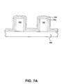
- FIG. 7A is a side sectional view of the faceplate and matrix structure of FIG. 1A taken along line A—A wherein the matrix structure has a contaminant prevention structure comprised of a layer of porous material and a layer of non-porous material disposed thereover in accordance with one embodiment of the present claimed invention.
- FIG. 7B is a side sectional view of the faceplate and matrix structure of FIG. 7A having a conductive coating disposed thereover in accordance with one embodiment of the present claimed invention.
- FIG. 8 is a side sectional view of the faceplate and matrix structure wherein the matrix structure has a dye/pigment-containing contaminant prevention structure disposed thereover in accordance with one embodiment of the present claimed invention.
- FIG. 9 is a side sectional view of a protected faceplate structure in which is shown a faceplate having a barrier layer disposed thereover in accordance with one embodiment of the present claimed invention.
- FIG. 10 is a side sectional view of a protected cathode substrate structure in which is shown a cathode substrate having a barrier layer disposed thereover in accordance with one embodiment of the present claimed invention.
- FIG. 11 is a flow chart of steps performed to provide a protected substrate structure in accordance with one embodiment of the present claimed invention.
- FIG. 1A shows a perspective view of a faceplate 100 of a flat panel display device having a matrix structure 102 coupled thereto.
- matrix structure 102 is located on faceplate 100 such that the row and columns of matrix structure 102 separate adjacent sub-pixel regions, typically shown as 104 .
- matrix structure 102 is formed of polyimide material.
- matrix structure 102 is formed of polyimide material in the present embodiment, the present invention is also well suited to use with various other matrix forming materials which may cause deleterious contamination.
- the present invention is also well suited for use with a matrix structure which is comprised of a photosensitive polyimide formulation containing components other than polyimide.
- matrix structure 102 is a “multi-level” matrix structure. That is, the rows of matrix structure 102 have a different height than the columns of matrix structure 102 .
- Such a multi-level matrix structure is shown in the embodiment of FIG. 1A in order to more clearly show sub-pixel regions 104 .
- the present invention is, however, well suited to use with a matrix structure which is not multi-level.
- the matrix structure of the present invention is sometimes referred to as a black matrix, it will be understood that the term “black” refers to the opaque characteristic of the matrix structure. That is, the present invention is also well suited to having a color other than black.
- the present invention is also well suited for use with various other physical components of a flat panel display device.
- some embodiments of the present invention refer to a matrix structure for defining pixel and/or sub-pixel regions of the flat panel display, the present invention is also well suited to an embodiment in which the pixel/sub-pixel defining structure is not a “matrix” structure. Therefore, for purposes of the present application, the term matrix structure refers to a pixel and/or sub-pixel defining structure and not to a particular physical shape of the structure.
- FIG. 1B a perspective view of a support structure 150 adapted to be encapsulated by a contaminant prevention structure in accordance with one embodiment of the present claimed invention is shown.
- support structure 150 is encapsulated by a contaminant prevention structure. That is, the contaminant prevention structure has a physical structure such that contaminants originating within support structure 150 are confined within support structure 150 . Thus, the contaminant prevention structure prevents contaminants which are generated within support structure 150 from migrating outside of support structure 150 .
- support structure 150 In addition to confining contaminants within support structure 150 , the material comprising the contaminant prevention structure of the present invention does not outgas contaminants when struck by electrons emitted from a cathode portion of the flat panel display.
- support structure 150 is a wall in the embodiment of FIG. 1B
- the present invention is also well suited to an embodiment in which the support structure is comprised, for example, of pins, balls, columns, or various other supporting structures.
- focus structure 160 is encapsulated by a contaminant prevention structure. That is, the contaminant prevention structure has a physical structure such that contaminants originating within focus structure 160 are confined within focus structure 160 . Thus, the contaminant prevention structure prevents contaminants which are generated within focus structure 160 from migrating outside of focus structure 160 .
- the material comprising the contaminant prevention structure of the present invention does not outgas contaminants when struck by electrons emitted from a cathode portion of the flat panel display.
- focus structure 160 is a waffle-like structure in the embodiment of FIG. 1C
- the present invention is also well suited to an embodiment in which the focus structure has a different shape.
- FIG. 2 a side sectional view of faceplate 100 and matrix structure 102 taken along line A—A of FIG. 1A is shown.
- the side sectional view only a portion of matrix structure 102 is shown for purposes of clarity. It will be understood, however, that the following steps are performed over a much larger portion of matrix structure 102 and are not limited only to those portion of matrix structure 102 shown in FIG. 2 . Additionally, the following steps used in the formation of the present invention are also well suited to an approach in which a preliminary bake-out step is used to initially purge some of the contaminants from the matrix. In a bake-out step, the matrix is heated prior to placing the matrix in the sealed vacuum environment of the flat panel display.
- a contaminant prevention structure 106 is disposed covering matrix structure 102 .
- contaminant prevention structure 106 is comprised of a layer of substantially non-porous material. That is, matrix structure 102 has a physical structure such that contaminants originating within matrix structure 102 are confined within matrix structure 102 . Thus, contaminant prevention structure 106 prevents contaminants which are generated within matrix structure 102 from migrating outside of matrix structure 102 .
- the material comprising contaminant prevention structure 106 of the present invention does not outgas contaminants when struck by electrons emitted from a cathode portion of the flat panel display.
- arrow 108 depicts the path of a contaminant generated within matrix structure 102 .
- contaminants include species such as, for example, N 2 , H 2 , CH 4 , CO, CO 2 , O 2 , and H 2 O.
- contaminant prevention structure 106 prevents contaminants from being emitted from matrix structure 102 .
- contaminant prevention structure 106 is comprised of a substantially non-porous material.
- the substantially non-porous material of contaminant prevention structure 106 is selected from the group consisting of: silicon oxide, a metal film, an inorganic solid, and the like.
- the substantially nonporous material of contaminant prevention structure 106 is comprised of an oxide, or oxides, of the lanthanide series. Moreover, in one embodiment, the substantially non-porous material of contaminant prevention structure 106 is selected from the group consisting of: Y 2 O 3 , La 2 O 3 , CeO 2 , Pr 4 O 11 , Nd 2 O 3 , Pm 2 O 3 , Sm 2 O 3 , EuO 2 , Gd 2 O 3 , TbO 2 , Dy 2 O 3 , Ho 2 O 3 , Er 2 O 3 , Tm 2 O 3 , Yb 2 O 3 , Yb 2 O 3 and Lu 2 O 3 , and their mixtures.
- the stoichiometries presented herein are exemplary and the present invention is well suited to the use of various other stoichiometries.
- the contaminant prevention structure 106 is comprised of an oxide, or oxides, of the lanthanide series
- oxides of the lanthanide series are transparent to visible light due to a wide band gap (e.g. approximately 5 eV).
- oxides of the lanthanide series have a lower oxygen loss/emission under electron bombardment because of stronger oxygen-metal bonding.
- oxides of the lanthanide series exhibit oxygen-metal bonding which is approximately 40 percent greater than the oxygen-metal bonding associated with silicon dioxide.
- the thickness of the contaminant structure can be reduced by a factor of four. That is, because of the higher atomic number and densities, the electron stopping distance in the lanthanide oxide-based contaminant structure is reduced by a factor of four compared to a contaminant structure formed of silicon dioxide.
- the substantially non-porous material of contaminant prevention structure 106 is comprised of a material selected from the group consisting of: high density oxides, nitride, Gd 2 O 3 , Yb 2 O 3 , HfO 2 , GdN x , HfN x , and their mixtures.
- the stoichiometries presented herein are exemplary and the present invention is well suited to the use of various other stoichiometries. Compared with materials such as, for example, SiO 2 and SiN x , the above listed materials are far more efficient in blocking electrons at energies greater than 10 keV.
- the above-listed materials match more closely to that of the D263 glass in coefficients of thermal expansion (CTE), As a result, the above-listed materials alleviate problems associated with glass cracking and bending. Also in the present embodiment, the materials used may be semi transparent as opposed to transparent such that transmission is greater than approximately 50 percent for optical wavelengths.
- the present embodiment is also well suited to the use of material such as aluminum, beryllium, and chemical vapor deposited silicon oxide for non-porous prevention structure 106 .
- the present invention is well suited to an embodiment in which the material of non-porous prevention structure 106 is a solid with a melting point of greater than approximately 500 degrees Celsius.
- the substantially non-porous material is deposited over matrix structure 102 by chemical vapor deposition (CVD), evaporation, sputtering, or other means, to a thickness of approximately 50-500 nanometers.
- CVD chemical vapor deposition
- evaporation evaporation
- sputtering or other means, to a thickness of approximately 50-500 nanometers.
- the present invention is well suited to the use of various other substantially non-porous materials which are suited to confining contaminants within matrix structure 102 .
- the present invention is also well suited to varying the thickness of contaminant prevention structure 106 to greater than or less than the thickness range
- contaminant prevention structure 106 has a thickness which is sufficient to prevent penetration by electrons directed towards faceplate 100 .
- contaminant prevention structure 106 is comprised of a layer of silicon dioxide deposited covering matrix 102 by CVD, evaporation, sputtering, or other means, to a thickness of approximately 100-500 nanometers.
- the contaminant prevention structure prevents penetration therethrough by electrons
- the contaminant prevention structure does not hermetically seal the underlying component.
- silicon dioxide is specifically recited as the barrier layer material in one embodiment
- an oxide or oxides of the lanthanide series are recited in another embodiment
- the present invention (including each of the above-listed embodiments, and each of the below listed embodiments is also well suited to the use of Al 2 O 3 , CrO x , ZnO, Si 3 N 4 , SiO 2 , TaO 5 , Tin Oxide, ITO, ZrO 2 , Y 2 O 3 , TiO 2 , and MgO and combinations thereof as the barrier layer material.
- contaminant prevention structure 106 again has a thickness which is sufficient to prevent penetration by electrons directed towards faceplate 100 .
- contaminant prevention structure 106 is comprised of a layer of oxide or oxides of the lanthanide series (e.g.
- the stoichiometries presented herein are exemplary and the present invention is well suited to the use of various other stoichiometries.
- such an embodiment confines thermally generated contaminants within or on the surface of matrix structure 102 , and further prevents contaminants from being formed by electron stimulated desorption. That is, the present embodiment substantially eliminates a major deleterious condition associated with electron bombardment of matrix structure 102 .
- the contaminant prevention structure prevents penetration therethrough by electrons, the contaminant prevention structure does not hermetically seal the underlying component.
- the present invention (including each of the above-listed embodiments, and each of the below listed embodiments is also well suited to the use of Al 2 O 3 , CrO x , ZnO, Si 3 N 4 , SiO 2 , TaO 5 , Tin Oxide, ITO, ZrO 2 , Y 2 O 3 , TiO 2 , and MgO and combinations thereof as the barrier layer material.
- contaminant prevention structure 106 is comprised of a material selected from the group consisting of: high density oxides, nitride, Gd 2 O 3 , Yb 2 O 3 , HfO 2 , GdN x , HfN x , and their mixtures.
- a material selected from the group consisting of: high density oxides, nitride, Gd 2 O 3 , Yb 2 O 3 , HfO 2 , GdN x , HfN x , and their mixtures.
- the stoichiometries presented herein are exemplary and the present invention is well suited to the use of various other stoichiometries.
- the above listed materials are far more efficient in blocking electrons at energies greater than 10 keV.
- the above-listed materials match more closely to that of the D263 glass in coefficients of thermal expansion (CTE).
- CTE coefficients of thermal expansion
- the above-listed materials alleviate problems associated with glass cracking and bending
- a multi-layer contaminant prevention structure is disposed covering matrix structure 102 .
- the multi-layer contaminant prevention structure is comprised of a plurality of layers, 106 and 110 , of substantially non-porous material. That is, matrix structure 102 has a physical structure such that contaminants originating within matrix structure 102 are confined within matrix structure 102 .
- the present multi-layer contaminant prevention structure prevents contaminants which are generated within matrix structure 102 from migrating outside of matrix structure 102 .
- layers 106 and 110 comprising the multi-layer contaminant prevention structure of the present invention do not outgas contaminants when struck by electrons emitted from a cathode portion of the flat panel display.
- arrow 108 depicts the path of a contaminant generated within matrix structure 102 .
- contaminants include species such as, for example, N 2 , H 2 , CH 4 , CO, CO 2 , O 2 , and H 2 O.
- the present multi-layer contaminant prevention structure prevents contaminants from being emitted from matrix structure 102 .
- multi-layer contaminant prevention structure is comprised of a plurality of layers of substantially non-porous material.
- at least one of the substantially non-porous layers of material, 106 and 110 , of the multi-layer contaminant prevention structure is selected from the group consisting of: silicon dioxide; a metal film; an inorganic solid, Al 2 O 3 , CrO x , ZnO, Si 3 N 4 , SiO 2 , TaO 5 , Tin Oxide, ITO, ZrO 2 , Y 2 O 3 , TiO 2 , and MgO, a layer of oxide, or oxides, of the lanthanide series, and combinations thereof and the like.
- the present embodiment is also well suited to the use of material such as aluminum, beryllium, and chemical vapor deposited silicon oxide for at least one of the substantially non-porous layers of material 106 and 110 .
- the present invention is well suited to an embodiment in which at least one of the non-porous layers of material 106 and 110 is comprised of a solid with a melting point of greater than approximately 500 degrees Celsius.
- at least one of layers 106 and 110 is deposited over matrix structure 102 by chemical vapor deposition (CVD), evaporation, sputtering, or other means.
- the multi-layer contaminant prevention structure has a total thickness of approximately 50-2000 nanometers.
- the present invention is well suited to the use of various other substantially non-porous materials which are suited to confining contaminants within matrix structure 102 .
- the present invention is also well suited to varying the total thickness of the multi-layer contaminant prevention structure to greater than or less than the thickness range listed above.
- the present invention is also well suited to varying the number of layers of substantially non-porous material which comprise the multi-layer contaminant prevention structure.
- the multi-layer contaminant prevention structure has a thickness which is sufficient to prevent penetration by electrons directed towards faceplate 100 .
- the multi-layer contaminant prevention structure includes a layer of silicon dioxide deposited covering matrix 102 by CVD to a thickness of approximately 100-2000 nanometers.
- the multi-layer contaminant prevention structure has a thickness which is sufficient to prevent penetration by electrons directed towards faceplate 100 .
- the multi-layer contaminant prevention structure includes a layer comprised of an oxide, or oxides, of the lanthanide series deposited covering matrix 102 by CVD to a thickness of approximately 25-125 nanometers.
- a contaminant prevention structure 112 is disposed covering matrix structure 102 and the sub-pixel regions 114 of faceplate 100 .
- the substantially non-porous material is a transparent material such as an oxide, or oxides of the lanthanide series, silicon dioxide, or indium tin oxide which is deposited over matrix structure 102 and sub-pixel regions 114 by chemical vapor deposition (CVD), evaporation, sputtering, or other means, to a thickness of approximately 10-500 nanometers.
- CVD chemical vapor deposition
- contaminant prevention structure 112 extends into sub-pixel regions 114 , the presence of, for example, the oxide or oxides of the lanthanide series material in sub-pixel regions 114 does not adversely affect the formation or operation of the flat panel display. It will be understood, however, that the present invention is well suited to the use of various other substantially non-porous materials which are suited to confining contaminants within matrix structure 102 and which do not adversely affect the formation or operation of the flat panel display. The present invention is also well suited to varying the thickness of contaminant prevention structure 112 to greater than or less than the thickness range listed above.
- the contaminant prevention structure 112 has a thickness which is sufficient to prevent penetration by electrons directed towards faceplate 100 .
- the present embodiment confines thermally generated contaminants within matrix structure 102 , and further prevents contaminants from being formed by electron stimulated desorption. That is, the present embodiment substantially eliminates a major deleterious condition associated with electron bombardment of matrix structure 102 .
- conductive coating 116 is disposed covering a contaminant prevention structure 106 .
- the present embodiment depicts the embodiment of FIG. 2 , having conductive coating 116 disposed thereover.
- conductive coating is preferably comprised of a low atomic number material.
- a low atomic number material refers to a material comprised of elements having atomic numbers of less than 18. Additionally, a low atomic number material will reduce the electron scattering compared to a high atomic number material.
- conductive coating 116 is comprised, for example, of a CB800A DAG made by Acheson Colloids of Port Huron, Mich.
- conductive coating 116 is comprised of a carbon-based conductive material.
- the layer of carbon-based conductive material is applied as a semi-dry spray to reduce shrinkage of conductive coating 116 .
- the present invention allows for improved control over the final depth of conductive coating 116 .
- deposition methods are recited above, it will be understood that the present invention is also well suited to using various other deposition methods to deposit various other conductive coatings over contaminant prevention structure 106 .
- the present invention is also well suited to the use of an aluminum coating which is applied by an angled evaporation.
- the top surface of matrix structure 102 is physically closer to the field emitter than is faceplate 100 .
- the present embodiment provides a constant potential surface.
- the present embodiment reduces the possibility of potential arcing.
- the present embodiment helps to ensure that the integrity of the phosphors and the overlying aluminum layer (not yet deposited in the embodiment of FIG. 5A ) is maintained.
- the conductive encapsulating layer can be made more electrically or thermally conductive than the aluminum layer over the phosphor by making it thicker or of a more conductive material, thereby enabling the encapsulating material to readily prevent localized voltage spikes by carrying off high electrical currents of potential arcs and to better physically withstand any arcs that may occur.
- the conductive coating can be a single layer (as in FIG. 2 ) on the black matrix and need not be a double layer as drawn.
- a conductive coating 116 is disposed covering layers 106 and 110 of a multi-layer contaminant prevention structure.
- the present embodiment depicts the embodiment of FIG. 3 , having conductive coating 116 disposed thereover.
- conductive coating is preferably comprised of a low atomic number material, or a material comprised predominantly of low atomic number elements.
- a low atomic number material refers to a material comprised of elements having atomic numbers of less than 18.
- conductive coating 116 is comprised, for example, of a CB800A DAG made by Acheson Colloids of Port Huron, Mich.
- conductive coating 116 is comprised of a carbon-based conductive material.
- the layer of carbon-based conductive material is applied as a semidry spray to reduce shrinkage of conductive coating 116 .
- the present invention allows for improved control over the final depth of conductive coating 116 .
- deposition methods are recited above, it will be understood that the present invention is also well suited to using various other deposition methods to deposit various other conductive coatings over layers 106 and 110 of the multi-layer contaminant prevention structure.
- the present invention is also well suited to the use of an aluminum coating which is applied by an angled evaporation.
- the present embodiment provides a constant potential surface and decreases the chances that any electrical arcing will occur. As a result, the present embodiment helps to ensure that the integrity of the phosphors and the overlying aluminum layer (not yet deposited in the embodiment of FIG. 5B ) is maintained.
- conductive coating 116 is disposed over contaminant prevention structure 112 .
- the present embodiment depicts the embodiment of FIG. 4 , having conductive coating 116 disposed thereover.
- conductive coating is preferably comprised of a low atomic number material. More specifically, in one embodiment, conductive coating 116 is comprised, for example, of a CB800A DAG made by Acheson Colloids of Port Huron, Mich. In another embodiment, conductive coating 116 is comprised of a carbon-based conductive material. In still another embodiment, the layer of carbon-based conductive material is applied as a semidry spray to reduce shrinkage of conductive coating 116 .
- the present invention allows for improved control over the final depth of conductive coating 116 .
- deposition methods are recited above, it will be understood that the present invention is also well suited to using various other deposition methods to deposit various other conductive coatings over contaminant prevention structure 112 .
- the present invention is also well suited to the use of an aluminum coating which is applied by an angled evaporation.
- the present embodiment provides a constant potential surface and decreases the chances that any electrical arcing will occur. As result, the present embodiment helps to ensure that the integrity of the phosphors and the overlying aluminum layer (not yet deposited in the embodiment of FIG. 5C ) is maintained.
- the present invention eliminates deleterious browning and outgassing associated with prior art polyimide based black matrix structures. Additionally, by preventing contaminants from being emitted by the matrix structure, the present invention prevents coating of the field emitters by the released contaminants. Additionally, by reducing the number and energy of electrons striking the polyimide, electron desorption of contaminants is reduced. As a result, the present invention extends the life of the field emitters. As yet an additional advantage, the contaminant prevention structure of the present invention also protects the matrix structure from potential damage during subsequent processing steps, and electrical arcs.
- matrix structure 102 is formed of polyimide material in the present embodiment.
- the present invention is also well suited to use with various other matrix forming materials which may cause deleterious contamination.
- the present invention is also well suited for use with a matrix structure which is comprised of a photosensitive polyimide formulation containing components other than polyimide.
- the present invention is also well suited for use with various other physical components such as, for example, support structures and/or focus structures.
- a contaminant prevention structure 602 is disposed covering matrix structure 102 and the sub-pixel regions 114 of faceplate 100 .
- contaminant prevention structure 602 extends into sub-pixel or pixel regions 114 , the presence of the transparent porous or non-porous material in sub-pixel or pixel regions 114 does not adversely affect the formation or operation of the flat panel display. It will be understood, however, that the present invention is well suited to an embodiment in which the porous material of contaminant prevention structure 602 does not extend into sub pixel regions 114 .
- contaminant prevention structure 106 is comprised of a layer of porous material.
- the porous material comprising contaminant prevention structure 602 prevents electrons and X-rays generated within the flat panel display from striking matrix structure 102 . Additionally, the material comprising contaminant prevention structure 602 of the present invention does not outgas contaminants when struck by electrons or X-rays generated within the flat panel display. It will be understood that such contaminants include species such as, for example, N 2 , H 2 , CH 4 , CO, CO 2 , O 2 , and H 2 O.
- contaminant prevention structure 602 is comprised of a porous material.
- the porous material of contaminant prevention structure 602 is selected from the group consisting of: colloidal silica; silicon oxide; chemical vapor deposited silicon oxide, and an oxide or oxides of the lanthanide series (e.g.
- porous contaminant prevention structure 602 is a solid with a melting point of greater than approximately 500 degrees Celsius.
- the porous material of contaminant prevention structure 602 is comprised of a material selected from the group consisting of: high density oxides, nitride, Gd 2 O 3 , Yb 2 O 3 , HfO 2 , GdN x , HfN x , and their mixtures.
- the stoichiometries presented herein are exemplary and the present invention is well suited to the use of various other stoichiometries. Compared with materials such as, for example, SiO 2 and SiN x , the above listed materials are far more efficient in blocking electrons at energies greater than 10 keV.
- the above-listed materials match more closely to that of the D263 glass in coefficients of thermal expansion (CTE).
- CTE coefficients of thermal expansion
- the above-listed materials alleviate problems associated with glass cracking and bending.
- the materials used may be semi transparent as opposed to transparent such that transmission is greater than approximately 50 percent for optical wavelengths.
- the porous material is silicon dioxide which is deposited over matrix structure 102 by atmospheric pressure physical vapor deposition (APPVD) or atmospheric pressure chemical vapor deposition (APCVD) to a thickness of approximately 3-10,000 nanometers.
- APSVD atmospheric pressure physical vapor deposition
- APCVD atmospheric pressure chemical vapor deposition
- the present invention is well suited to the use of various other porous materials which are suited to preventing electron and/or X-ray penetration therethrough by electrons and/or X-rays generated in the flat panel display.
- the present invention is also well suited to an embodiment in which the layer of porous material is applied, for example, by sputtering, e-beam evaporation, spraying methods; dip-coating methods, and the like.
- the present invention is also well suited to varying the thickness of contaminant prevention structure 602 to greater than or less than the thickness range listed above. More specifically, at 6 keV, the vast majority of electrons will not penetrate farther than 600 nanometers into silicon dioxide. At 10 keV, the vast majority of electrons will not penetrate farther than 1,000 nanometers into silicon dioxide. Therefore, in the present embodiment, the depth of the porous material comprising contaminant prevention structure 602 is adjusted so as to ensure that matrix structure 102 is not bombarded by electrons and/or X-rays generated within the flat panel display.
- the porous material is an oxide or oxides of the lanthanide series which is deposited over matrix structure 102 by atmospheric pressure physical vapor deposition (APPVD) or atmospheric pressure chemical vapor deposition (APCVD) to a thickness of approximately 7-250 nanometers.
- APPVD atmospheric pressure physical vapor deposition
- APCVD atmospheric pressure chemical vapor deposition
- the present invention is also well suited to an embodiment in which the layer of porous material is applied, for example, by sputtering, e-beam evaporation, spraying methods, dip-coating methods, and the like.
- the present invention is also well suited to varying the thickness of contaminant prevention structure 602 to greater than or less than the thickness range listed above. More specifically, at 6 keV, the vast majority of electrons will not penetrate farther than 600 nanometers into silicon dioxide. At 10 keV, the vast majority of electrons will not penetrate farther than 250 nanometers into an oxide or oxides of the lanthanide series. Therefore, in the present embodiment, the depth of the porous material comprising contaminant prevention structure 602 is adjusted so as to ensure that matrix structure 102 is not bombarded by electrons and/or X-rays generated within the flat panel display.
- a multi-layer contaminant prevention structure is disposed covering matrix structure 102 .
- the multi-layer contaminant prevention structure is comprised of a plurality of layers, 602 and 604 , of porous material.
- the present embodiment prevents electrons and X-rays generated within the flat panel display from striking matrix structure 102 .
- the material comprising the contaminant prevention structure of the present invention does not outgas contaminants when struck by electrons or X-rays generated within the flat panel display.
- multi-layer contaminant prevention structure is comprised of a plurality of layers of porous material.
- at least one of the layers of porous material, 602 and 604 , of the multi-layer contaminant prevention structure is selected from the group consisting of: colloidal silica; silicon oxide; chemical vapor deposited silicon oxide; and an oxide or oxides of the lanthanide series.
- colloidal silica silicon oxide
- chemical vapor deposited silicon oxide silicon oxide
- oxide or oxides of the lanthanide series oxide or oxides of the lanthanide series.
- the present invention is also well suited to use with various other porous materials such as, for example, silicon, oxides, nitrides, carbides, graphite, aluminum, diamond, and the like.
- the present invention is well suited to an embodiment in which at least one of the layers of porous material 602 and 604 is a solid with a melting point of greater than approximately 500 degrees Celsius.
- the porous material of at least one of layers 602 and 604 is silicon dioxide which is deposited over matrix structure 102 by atmospheric pressure physical vapor deposition (APPVD) or atmospheric pressure chemical vapor deposition (APCVD) to a thickness of approximately 3-10,000 nanometers.
- APSVD atmospheric pressure physical vapor deposition
- APCVD atmospheric pressure chemical vapor deposition
- the present invention is also well suited to an embodiment in which the layer of porous material is applied, for example, by sputtering, e-beam evaporation, spraying methods, dip-coating methods, and the like.
- the present invention is also well suited to varying the thickness of contaminant prevention structure to greater than or less than the thickness range listed above.
- the combined depth of the layers of porous material 602 and 604 comprising the contaminant prevention structure is adjusted so as to ensure that matrix structure 102 is not bombarded by electrons and/or X-rays generated within the flat panel display.
- the porous material of at least one of layers 602 and 604 is an oxide, or oxides, of the lanthanide series which is deposited over matrix structure 102 by atmospheric pressure physical vapor deposition (APPVD) or atmospheric pressure chemical vapor deposition (APCVD) to a thickness of approximately 7-250 nanometers.
- APPVD atmospheric pressure physical vapor deposition
- APCVD atmospheric pressure chemical vapor deposition
- the present invention is also well suited to an embodiment in which the layer of porous material is applied, for example, by sputtering, e-beam evaporation, spraying methods, dip-coating methods, and the like.
- the present invention is also well suited to varying the thickness of contaminant prevention structure to greater than or less than the thickness range listed above.
- the combined depth of the layers of porous material 602 and 604 comprising the contaminant prevention structure is adjusted so as to ensure that matrix structure 102 is not bombarded by electrons and/or X-rays generated within the flat panel display.
- conductive coating 606 is disposed over a contaminant prevention structure.
- the present embodiment depicts the embodiment of FIG. 6B having conductive coating 606 disposed thereover.
- the present invention is, however, well suited to an embodiment in which conductive coating 606 is disposed over, for example, the embodiment of FIG. 6 A.
- conductive coating is preferably comprised of a low atomic number material. More specifically, in one embodiment, conductive coating 606 is comprised, for example, of a CB800A DAG made by Acheson Colloids of Port Huron, Mich. In another embodiment, conductive coating 606 is comprised of a carbon-based conductive material.
- the layer of carbon-based conductive material is applied as a semi-dry spray to reduce shrinkage of conductive coating 606 .
- the present invention allows for improved control over the final depth of conductive coating 606 .
- conductive coating 606 is deposited to a depth of 100-500 nanometers.
- the present embodiment provides a constant potential surface and decreases the chances that any electrical arcing will occur. As result, the present embodiment helps to ensure that the integrity of the phosphors and the overlying aluminum layer (not yet deposited in the embodiment of FIG. 6C ) is maintained.
- a multi-layer contaminant prevention structure is disposed covering matrix structure 102 .
- the multi-layer contaminant prevention structure is comprised of a plurality of layers, 702 and 704 .
- layer 702 is comprised of a porous material
- layer 704 is comprised of a layer of substantially non-porous material.
- the present embodiment prevents electrons and X-rays generated within the flat panel display from striking matrix structure 102 . This embodiment further confines thermally generated contaminants within matrix structure 102 .
- the material comprising the contaminant prevention structure of the present invention does not outgas contaminants when struck by electrons or X-rays generated within the flat panel display.
- the multi-layer contaminant prevention structure is comprised of a plurality of layers of material.
- porous material, 702 of the multi-layer contaminant prevention structure is selected from the group consisting of: colloidal silica; silicon oxide; and chemical vapor deposited silicon oxide. It will be understood, however, that the present invention is also well suited to use with various other porous materials such as, for example, silicon, oxides, nitrides, carbides, diamond, and the like. Moreover, the present invention is well suited to an embodiment in which at least one of the layers of material 702 and 704 is a solid with a melting point of greater than approximately 500 degrees Celsius.
- the plurality of layers of material are defined as follows.
- Layer 702 is comprised of a layer of indium tin oxide which is deposited to a depth of approximately 100-1,000 nanometers.
- Layer 704 is comprised of a silicon oxide which is deposited over matrix structure 102 to a thickness of approximately 30-1,000 nanometers. It will be understood, however, that the present invention is well suited to the use of various other porous and non-porous materials. The present invention is also well suited to an embodiment in which the layer of porous material is applied, for example, by sputtering, e-beam evaporation, spraying methods, dip-coating methods, and the like.
- the present invention is also well suited to varying the thickness of the contaminant prevention structure to greater than or less than the thickness range listed above.
- the combined depth of the layers of material 702 and 704 comprising the contaminant prevention structure is adjusted so as to ensure that matrix structure 102 is not bombarded by electrons and/or X-rays generated within the flat panel display.
- the plurality of layers of material are defined as follows.
- Layer 702 is comprised of a layer of indium tin oxide which is deposited to a depth of approximately 100-1,000 nanometers.
- Layer 704 is comprised of an oxide, or oxides, of the lanthanide series which is deposited over matrix structure 102 to a thickness of approximately 7-250 nanometers. It will be understood, however, that the present invention is well suited to the use of various other porous and non-porous materials. The present invention is also well suited to an embodiment in which the layer of porous material is applied, for example, by sputtering, e-beam evaporation, spraying methods, dip-coating methods, and the like.
- the present invention is also well suited to varying the thickness of the contaminant prevention structure to greater than or less than the thickness range listed above.
- the combined depth of the layers of material 702 and 704 comprising the contaminant prevention structure is adjusted so as to ensure that matrix structure 102 is not bombarded by electrons and/or X-rays generated within the flat panel display.
- FIG. 7B another embodiment of the present invention is shown in which a conductive coating 706 is disposed over a contaminant prevention structure.
- the present embodiment depicts one embodiment of FIG. 7A having conductive coating 706 disposed thereover.
- layer 702 is comprised of a layer of indium tin oxide which is deposited to a depth of approximately 100-1,000 nanometers.
- Layer 704 is comprised of a silicon oxide which is deposited over matrix structure 102 to a thickness of approximately 30-1,000 nanometers.
- Layer 706 of this embodiment is comprised of a layer of aluminum which is deposited to a depth of approximately 30-200 nanometers.
- the conductive coating is preferably comprised of a low atomic number material.
- conductive coating 606 is comprised, for example, of a CB800A DAG made by Acheson Colloids of Port Huron, Mich.
- conductive coating 606 is comprised of a carbon-based conductive material.
- the layer of carbon-based conductive material is applied as a semi-dry spray to reduce shrinkage of conductive coating 606 .
- the present invention allows for improved control over the final depth of conductive coating 606 .
- deposition methods are recited above, it will be understood that the present invention is also well suited to using various other deposition methods to deposit various other conductive coatings (e.g. aluminum) over the contaminant prevention structure.
- conductive coating 706 is again disposed over a contaminant prevention structure.
- the present embodiment depicts one embodiment of FIG. 7A having conductive coating 706 disposed thereover.
- layer 702 is comprised of a layer of indium tin oxide which is deposited to a depth of approximately 100-1,000 nanometers.
- layer 704 is comprised of an oxide or oxides of the lanthanide series which is deposited over matrix structure 102 to a thickness of approximately 7-250 nanometers.
- Layer 706 of this embodiment is comprised of a layer of aluminum which is deposited to a depth of approximately 30-200 nanometers.
- the conductive coating is preferably comprised of a low atomic number material. More specifically, in one embodiment, conductive coating 606 is comprised, for example, of a CB800A DAG made by Acheson Colloids of Port Huron, Mich. In another embodiment, conductive coating 606 is comprised of a carbon-based conductive material. In still another embodiment, the layer of carbon-based conductive material is applied as a semi-dry spray to reduce shrinkage of conductive coating 606 . In so doing, the present invention allows for improved control over the final depth of conductive coating 606 . Although such deposition methods are recited above, it will be understood that the present invention is also well suited to using various other deposition methods to deposit various other conductive coatings (e.g. aluminum) over the contaminant prevention structure.
- conductive coating 606 is comprised, for example, of a CB800A DAG made by Acheson Colloids of Port Huron, Mich.
- conductive coating 606 is comprised of a carbon-based conductive material.
- the contaminant structure is comprised of two distinct layers of material 702 and 704 .
- the contaminant prevention structure is comprised of a layer of porous material (e.g. layer 704 of silicon oxide) having non-porous material (e.g. the indium tin oxide of layer 702 ) impregnated therein. That is, the present invention is also well suited to an embodiment in which a layer of substantially porous material has substantially non-porous material impregnated therein. In one such embodiment, the layer of substantially porous material is deposited as is described above in detail.
- substantially nonporous material is impregnated within the layer of substantially non-porous material by, for example, sputtering, physical vapor deposition, and the like.
- present embodiment is also well suited to having a conductive coating disposed thereover as is describe above in great detail.
- the contaminant structure is comprised of two distinct layers of material 702 and 704 .
- the contaminant prevention structure is comprised of a layer of porous material (e.g. layer 704 of an oxide or oxides of the lanthanide series) having non-porous material (e.g. the indium tin oxide of layer 702 ) impregnated therein. That is, the present invention is also well suited to an embodiment in which a layer of substantially porous material has substantially non-porous material impregnated therein. In one such embodiment, the layer of substantially porous material is deposited as is described above in detail.
- substantially non-porous material is impregnated within the layer of substantially non-porous material by, for example, sputtering, physical vapor deposition, and the like.
- present embodiment is also well suited to having a conductive coating disposed thereover as is describe above in great detail.
- matrix structure 102 is formed of polyimide material in the present embodiment.
- the present invention is also well suited to use with various other matrix forming materials which may cause deleterious contamination.
- the present invention is also well suited for use with a matrix structure which is comprised of a photosensitive polyimide formulation containing components other than polyimide.
- the present invention is also well suited for use with various other physical components such as, for example, support structures and/or focus structures.
- contaminant prevention structure 802 is disposed over matrix structure 102 and into sub-pixel regions 114 .
- Contaminant prevention structure 802 further includes a selectively light absorbing components (e.g. a dye or pigment) typically shown as 804 .
- contaminant prevention structure 802 is comprised of silicon oxide doped with dye/pigment material.
- the present embodiment provides a color filter which enhances display contrast by reducing reflected ambient light.
- the present embodiment is well suited to having the dye/pigment disposed only in those portions of contaminant prevention structure 802 which reside above sub-pixel regions 114 .
- the present embodiment is also well suited to having the dye/pigment disposed in the entire contaminant prevention structure 802 .
- matrix structure 102 is formed of polyimide material in the present embodiment.
- the present invention is also well suited to use with various other matrix forming materials which may cause deleterious contamination.
- the present invention is also well suited for use with a matrix structure which is comprised of a photosensitive polyimide formulation containing components other than polyimide.
- the present invention is also well suited for use with various other physical components such as, for example, support structures and/or focus structures.
- contaminant prevention structure 802 is disposed over matrix structure 102 and into sub-pixel regions 114 .
- Contaminant prevention structure 802 further includes a selectively light absorbing components (e.g. a dye or pigment) typically shown as 804 .
- contaminant prevention structure 802 is comprised of an oxide or oxides of the lanthanide series doped with dye/pigment material.
- the present embodiment provides a color filter which enhances display contrast by reducing reflected ambient light.
- the present embodiment is well suited to having the dye/pigment disposed only in those portions of contaminant prevention structure 802 which reside above sub-pixel regions 114 .
- the present embodiment is also well suited to having the dye/pigment disposed in the entire contaminant prevention structure 802 .
- the present embodiment provides a constant potential surface and decreases the chances that any electrical arcing will occur. As result, the present embodiment helps to ensure that the integrity of the phosphors and the overlying aluminum layer (not yet deposited in the embodiment of FIG. 7B ) is maintained.
- the present invention provides a matrix structure which does not deleteriously outgas when subjected to thermal variations.
- the present invention also provides an embodiment in which a matrix structure meets the above-listed need and which reduces unwanted electron stimulated desorption of contaminants.
- the present invention provides a matrix structure which meets both of the above needs and which also achieves electrical robustness in the faceplate by providing a constant potential surface which reduces the possibility of potential arcing.
- the conductive matrix structure of the present invention is applicable in numerous types of flat panel displays.
- a faceplate 100 has a barrier layer 902 disposed over one side thereof.
- matrix structure 102 defines phosphor containing area (also referred to as sub-pixel regions) which are shown as areas 114 .
- phosphor containing area also referred to as sub-pixel regions
- a potential field Upon being impinged by the electrons, the phosphors within phosphor containing areas 114 generate light.
- barrier layer 902 prevents degradation of faceplate 100 by electron bombardment.
- barrier layer 902 is comprised of a substantially transparent, electron-damage resistant material.
- barrier layer 902 is deposited over faceplate 100 as one of the initial process steps performed in the formation of the field emission display device. That is, barrier layer 902 of the present embodiment is disposed above faceplate 100 prior to the formation of matrix 102 , and prior to the formation of phosphor containing areas 114 .
- the present invention is also well suited to varying the order in which the barrier layer and the various other features of the field emission display are fabricated.
- barrier layer 902 has a thickness sufficient to prevent substantial penetration of electrons through barrier layer 902 such that the electrons do not impinge faceplate 100 .
- barrier layer 902 is comprised of silicon dioxide having a thickness of approximately 100 nanometers.
- the present invention is well suited to the use of various other materials and/or to various (e.g. greater or lesser) thicknesses of material.
- the combination of material or materials and the thickness thereof provides a barrier layer which does not significantly reduce the transmission of light through the faceplate, and which protects the faceplate from electron bombardment induced degradation.
- barrier layer 902 is comprised of an oxide or oxides of the lanthanide series having a thickness of approximately 25 nanometers.
- the present invention is well suited to the use of various other materials and/or to various (e.g. greater or lesser) thicknesses of material.
- the combination of material or materials and the thickness thereof provides a barrier layer which does not significantly reduce the transmission of light through the faceplate, and which protects the faceplate from electron bombardment induced degradation.
- barrier layer 902 prevents the migration of contaminants from faceplate 100 into the field emission display device.
- faceplate 100 is no longer a potentially substantial source of contaminants which can damage sensitive features of the field emission display device.
- barrier layer 902 enables use of a desirable and inexpensive high-sodium glass substrate as faceplate 100 .
- the present embodiment prevents the migration of sodium from faceplate 100 into the field emission display device.
- barrier layer 902 in addition to preventing substantial impingement of electrons against faceplate 100 , and in addition to preventing the migration of contaminants from faceplate 100 into the field emission display device, barrier layer 902 is also electrically conductive. In so doing, barrier layer 902 can be used to bleed excess charge from faceplate 100 .
- a cathode substrate 1001 has a barrier layer 1002 disposed over one side thereof.
- field emitters typically shown as 1004
- field emitters 1004 are shown disposed above cathode substrate 1001 and between focus structure 160 .
- electrons are emitted from field emitters 1004 .
- These emitted electrons are then accelerated, using a potential field, towards phosphor containing areas, not shown.
- the phosphors within phosphor containing areas generate light.
- barrier layer 1002 prevents degradation of cathode substrate 1001 by electron bombardment.
- barrier layer 1002 is comprised of a substantially transparent, electron-damage resistant material.
- barrier layer 1002 is deposited over cathode substrate 1001 as one of the initial process steps performed in the formation of the field emission display device. That is, barrier layer 1002 of the present embodiment is disposed above cathode substrate 1001 prior to the formation of matrix field emitters 1004 , and prior to the formation of focus structure 160 .
- the present invention is also well suited to varying the order in which the barrier layer and the various other features of the field emission display are fabricated.
- barrier layer 1002 has a thickness sufficient to prevent substantial penetration of electrons through barrier layer 1002 such that the electrons do not impinge cathode substrate 1001 .
- barrier layer 1002 is comprised of silicon dioxide having a thickness of approximately 100 nanometers. Although such a specific type of material and thickness of material is recited in the present embodiment, the present invention is well suited to the use of various other materials and/or to various (e.g. greater or lesser) thicknesses of material.
- barrier layer 1002 is comprised of an oxide or oxides of the lanthanide series having a thickness of approximately 25 nanometers.
- barrier layer 1002 prevents the migration of contaminants from cathode substrate 1001 into the field emission display device.
- cathode substrate 1001 is no longer a potentially substantial source of contaminants which can damage sensitive features of the field emission display device.
- barrier layer 1002 enables use of a desirable and inexpensive high-sodium glass substrate as cathode substrate 1001 .
- barrier layer 1002 is also electrically conductive. In so doing, barrier layer 1002 can be used to bleed excess charge from cathode substrate 1001 .
- the present embodiment recites a method for protecting a substrate structure of a field emission display device.
- the present invention comprises at step 1102 , providing a substrate structure of a field emission display device.
- a substrate structure includes, for example, faceplate 100 of FIG. 9 or cathode substrate 1001 of FIG. 10 .
- the present invention enables the use of a high-sodium glass substrate structure for the field emission display device in one embodiment.
- barrier layer 1002 is comprised of a substantially transparent, electron-damage resistant material (e.g. silicon dioxide, Al 2 O 3 , CrO x , ZnO, Si 3 N 4 , SiO 2 , TaO 5 , Tin Oxide, ITO, ZrO 2 , Y 2 O 3 , TiO 2 , and MgO and combinations thereof) having a thickness (e.g. 100 nanometers) sufficient to prevent substantial penetration of electrons therethrough.
- a substantially transparent, electron-damage resistant material e.g. silicon dioxide, Al 2 O 3 , CrO x , ZnO, Si 3 N 4 , SiO 2 , TaO 5 , Tin Oxide, ITO, ZrO 2 , Y 2 O 3 , TiO 2 , and MgO and combinations thereof
- barrier layer 1002 is comprised of a substantially transparent, electron-damage resistant material (e.g. an oxide, or oxides, of the lanthanide series such as Y 2 O 3 , La 2 O 3 , CeO 2 , Pr 4 O 11 , Nd 2 O 3 , Pm 2 O 3 , Sm 2 O 3 , EuO 2 , Gd 2 O 3 , TbO 2 , Dy 2 O 3 , Ho 2 O 3 , Er 2 O 3 , Tm 2 O 3 , Yb 2 O 3 , Yb 2 O 3 and Lu 2 O 3 , and their mixtures) having a thickness (e.g. 25 nanometers) sufficient to prevent substantial penetration of electrons therethrough.
- a substantially transparent, electron-damage resistant material e.g. an oxide, or oxides, of the lanthanide series such as Y 2 O 3 , La 2 O 3 , CeO 2 , Pr 4 O 11 , Nd 2 O 3 , Pm 2 O 3 , Sm 2
- the barrier layer prevents the migration of contaminants from the substrate into the active region.
- the barrier layer is conductive such that it can be used to bleed excess charge from the substrate structure.
- the material of barrier layer 1002 is comprised of a material selected from the group consisting of: high density oxides, nitride, Gd 2 O 3 , Yb 2 O 3 , HfO 2 , GdN x , HfN x , and their mixtures.
- the stoichiometries presented herein are exemplary and the present invention is well suited to the use of various other stoichiometries.
- the above listed materials are far more efficient in blocking electrons at energies greater than 10 keV.
- the above-listed materials match more closely to that of the D263 glass in coefficients of thermal expansion (CTE).
- CTE coefficients of thermal expansion
- the above-listed materials alleviate problems associated with glass cracking and bending.
- the materials used may be semi transparent as opposed to transparent such that transmission is greater than approximately 50 percent for optical wavelengths.
Abstract
Description
Claims (12)
Priority Applications (1)
| Application Number | Priority Date | Filing Date | Title |
|---|---|---|---|
| US10/412,196 US6853129B1 (en) | 2000-07-28 | 2003-04-11 | Protected substrate structure for a field emission display device |
Applications Claiming Priority (3)
| Application Number | Priority Date | Filing Date | Title |
|---|---|---|---|
| US09/627,355 US7002287B1 (en) | 1998-05-29 | 2000-07-28 | Protected substrate structure for a field emission display device |
| US09/895,699 US6741027B1 (en) | 1998-05-29 | 2001-06-29 | Protected substrate structure for a field emission display device |
| US10/412,196 US6853129B1 (en) | 2000-07-28 | 2003-04-11 | Protected substrate structure for a field emission display device |
Related Parent Applications (1)
| Application Number | Title | Priority Date | Filing Date |
|---|---|---|---|
| US09/895,699 Continuation US6741027B1 (en) | 1998-05-29 | 2001-06-29 | Protected substrate structure for a field emission display device |
Publications (1)
| Publication Number | Publication Date |
|---|---|
| US6853129B1 true US6853129B1 (en) | 2005-02-08 |
Family
ID=34108158
Family Applications (1)
| Application Number | Title | Priority Date | Filing Date |
|---|---|---|---|
| US10/412,196 Expired - Fee Related US6853129B1 (en) | 2000-07-28 | 2003-04-11 | Protected substrate structure for a field emission display device |
Country Status (1)
| Country | Link |
|---|---|
| US (1) | US6853129B1 (en) |
Cited By (163)
| Publication number | Priority date | Publication date | Assignee | Title |
|---|---|---|---|---|
| US20020075555A1 (en) * | 1994-05-05 | 2002-06-20 | Iridigm Display Corporation | Interferometric modulation of radiation |
| US20040058532A1 (en) * | 2002-09-20 | 2004-03-25 | Miles Mark W. | Controlling electromechanical behavior of structures within a microelectromechanical systems device |
| US20040209192A1 (en) * | 2003-04-21 | 2004-10-21 | Prime View International Co., Ltd. | Method for fabricating an interference display unit |
| US20040240032A1 (en) * | 1994-05-05 | 2004-12-02 | Miles Mark W. | Interferometric modulation of radiation |
| US20040263944A1 (en) * | 2003-06-24 | 2004-12-30 | Miles Mark W. | Thin film precursor stack for MEMS manufacturing |
| US20050036095A1 (en) * | 2003-08-15 | 2005-02-17 | Jia-Jiun Yeh | Color-changeable pixels of an optical interference display panel |
| US20050046922A1 (en) * | 2003-09-03 | 2005-03-03 | Wen-Jian Lin | Interferometric modulation pixels and manufacturing method thereof |
| US20050046948A1 (en) * | 2003-08-26 | 2005-03-03 | Wen-Jian Lin | Interference display cell and fabrication method thereof |
| US20050078348A1 (en) * | 2003-09-30 | 2005-04-14 | Wen-Jian Lin | Structure of a micro electro mechanical system and the manufacturing method thereof |
| US20050122560A1 (en) * | 2003-12-09 | 2005-06-09 | Sampsell Jeffrey B. | Area array modulation and lead reduction in interferometric modulators |
| US20050142684A1 (en) * | 2002-02-12 | 2005-06-30 | Miles Mark W. | Method for fabricating a structure for a microelectromechanical system (MEMS) device |
| US20050168431A1 (en) * | 2004-02-03 | 2005-08-04 | Clarence Chui | Driver voltage adjuster |
| US20050247477A1 (en) * | 2004-05-04 | 2005-11-10 | Manish Kothari | Modifying the electro-mechanical behavior of devices |
| US20050249966A1 (en) * | 2004-05-04 | 2005-11-10 | Ming-Hau Tung | Method of manufacture for microelectromechanical devices |
| US20050250235A1 (en) * | 2002-09-20 | 2005-11-10 | Miles Mark W | Controlling electromechanical behavior of structures within a microelectromechanical systems device |
| US20050254115A1 (en) * | 2004-05-12 | 2005-11-17 | Iridigm Display Corporation | Packaging for an interferometric modulator |
| US20050277277A1 (en) * | 2000-10-13 | 2005-12-15 | Taiwan Semiconductor Manufacturing Company, Ltd. | Dual damascene process |
| US20050286113A1 (en) * | 1995-05-01 | 2005-12-29 | Miles Mark W | Photonic MEMS and structures |
| US20050286114A1 (en) * | 1996-12-19 | 2005-12-29 | Miles Mark W | Interferometric modulation of radiation |
| US20060001942A1 (en) * | 2004-07-02 | 2006-01-05 | Clarence Chui | Interferometric modulators with thin film transistors |
| US20060007517A1 (en) * | 2004-07-09 | 2006-01-12 | Prime View International Co., Ltd. | Structure of a micro electro mechanical system |
| US20060024880A1 (en) * | 2004-07-29 | 2006-02-02 | Clarence Chui | System and method for micro-electromechanical operation of an interferometric modulator |
| US20060044928A1 (en) * | 2004-08-27 | 2006-03-02 | Clarence Chui | Drive method for MEMS devices |
| US20060044246A1 (en) * | 2004-08-27 | 2006-03-02 | Marc Mignard | Staggered column drive circuit systems and methods |
| US20060057754A1 (en) * | 2004-08-27 | 2006-03-16 | Cummings William J | Systems and methods of actuating MEMS display elements |
| US20060066936A1 (en) * | 2004-09-27 | 2006-03-30 | Clarence Chui | Interferometric optical modulator using filler material and method |
| US20060065940A1 (en) * | 2004-09-27 | 2006-03-30 | Manish Kothari | Analog interferometric modulator device |
| US20060066503A1 (en) * | 2004-09-27 | 2006-03-30 | Sampsell Jeffrey B | Controller and driver features for bi-stable display |
| US20060066863A1 (en) * | 2004-09-27 | 2006-03-30 | Cummings William J | Electro-optical measurement of hysteresis in interferometric modulators |
| US20060066864A1 (en) * | 2004-09-27 | 2006-03-30 | William Cummings | Process control monitors for interferometric modulators |
| US20060067641A1 (en) * | 2004-09-27 | 2006-03-30 | Lauren Palmateer | Method and device for packaging a substrate |
| US20060066600A1 (en) * | 2004-09-27 | 2006-03-30 | Lauren Palmateer | System and method for display device with reinforcing substance |
| US20060066560A1 (en) * | 2004-09-27 | 2006-03-30 | Gally Brian J | Systems and methods of actuating MEMS display elements |
| US20060065436A1 (en) * | 2004-09-27 | 2006-03-30 | Brian Gally | System and method for protecting microelectromechanical systems array using back-plate with non-flat portion |
| US20060066938A1 (en) * | 2004-09-27 | 2006-03-30 | Clarence Chui | Method and device for multistate interferometric light modulation |
| US20060066856A1 (en) * | 2004-09-27 | 2006-03-30 | William Cummings | Systems and methods for measuring color and contrast in specular reflective devices |
| US20060066598A1 (en) * | 2004-09-27 | 2006-03-30 | Floyd Philip D | Method and device for electrically programmable display |
| US20060066601A1 (en) * | 2004-09-27 | 2006-03-30 | Manish Kothari | System and method for providing a variable refresh rate of an interferometric modulator display |
| US20060066541A1 (en) * | 2004-09-27 | 2006-03-30 | Gally Brian J | Method and device for manipulating color in a display |
| US20060067644A1 (en) * | 2004-09-27 | 2006-03-30 | Clarence Chui | Method of fabricating interferometric devices using lift-off processing techniques |
| US20060066595A1 (en) * | 2004-09-27 | 2006-03-30 | Sampsell Jeffrey B | Method and system for driving a bi-stable display |
| US20060067651A1 (en) * | 2004-09-27 | 2006-03-30 | Clarence Chui | Photonic MEMS and structures |
| US20060066559A1 (en) * | 2004-09-27 | 2006-03-30 | Clarence Chui | Method and system for writing data to MEMS display elements |
| US20060067648A1 (en) * | 2004-09-27 | 2006-03-30 | Clarence Chui | MEMS switches with deforming membranes |
| US20060065366A1 (en) * | 2004-09-27 | 2006-03-30 | Cummings William J | Portable etch chamber |
| US20060067600A1 (en) * | 2004-09-27 | 2006-03-30 | Gally Brian J | Display element having filter material diffused in a substrate of the display element |
| US20060067649A1 (en) * | 2004-09-27 | 2006-03-30 | Ming-Hau Tung | Apparatus and method for reducing slippage between structures in an interferometric modulator |
| US20060067643A1 (en) * | 2004-09-27 | 2006-03-30 | Clarence Chui | System and method for multi-level brightness in interferometric modulation |
| US20060066594A1 (en) * | 2004-09-27 | 2006-03-30 | Karen Tyger | Systems and methods for driving a bi-stable display element |
| US20060066599A1 (en) * | 2004-09-27 | 2006-03-30 | Clarence Chui | Reflective display pixels arranged in non-rectangular arrays |
| US20060066596A1 (en) * | 2004-09-27 | 2006-03-30 | Sampsell Jeffrey B | System and method of transmitting video data |
| US20060067646A1 (en) * | 2004-09-27 | 2006-03-30 | Clarence Chui | MEMS device fabricated on a pre-patterned substrate |
| US20060067642A1 (en) * | 2004-09-27 | 2006-03-30 | Karen Tyger | Method and device for providing electronic circuitry on a backplate |
| US20060065622A1 (en) * | 2004-09-27 | 2006-03-30 | Floyd Philip D | Method and system for xenon fluoride etching with enhanced efficiency |
| US20060066543A1 (en) * | 2004-09-27 | 2006-03-30 | Gally Brian J | Ornamental display device |
| US20060066937A1 (en) * | 2004-09-27 | 2006-03-30 | Idc, Llc | Mems switch with set and latch electrodes |
| US20060067652A1 (en) * | 2004-09-27 | 2006-03-30 | Cummings William J | Methods for visually inspecting interferometric modulators for defects |
| US20060066504A1 (en) * | 2004-09-27 | 2006-03-30 | Sampsell Jeffrey B | System with server based control of client device display features |
| US20060066932A1 (en) * | 2004-09-27 | 2006-03-30 | Clarence Chui | Method of selective etching using etch stop layer |
| US20060066597A1 (en) * | 2004-09-27 | 2006-03-30 | Sampsell Jeffrey B | Method and system for reducing power consumption in a display |
| US20060066876A1 (en) * | 2004-09-27 | 2006-03-30 | Manish Kothari | Method and system for sensing light using interferometric elements |
| US20060066542A1 (en) * | 2004-09-27 | 2006-03-30 | Clarence Chui | Interferometric modulators having charge persistence |
| US20060067650A1 (en) * | 2004-09-27 | 2006-03-30 | Clarence Chui | Method of making a reflective display device using thin film transistor production techniques |
| US20060065043A1 (en) * | 2004-09-27 | 2006-03-30 | William Cummings | Method and system for detecting leak in electronic devices |
| US20060077515A1 (en) * | 2004-09-27 | 2006-04-13 | Cummings William J | Method and device for corner interferometric modulation |
| US20060077617A1 (en) * | 2004-09-27 | 2006-04-13 | Floyd Philip D | Selectable capacitance circuit |
| US20060077508A1 (en) * | 2004-09-27 | 2006-04-13 | Clarence Chui | Method and device for multistate interferometric light modulation |
| US20060076637A1 (en) * | 2004-09-27 | 2006-04-13 | Gally Brian J | Method and system for packaging a display |
| US20060077502A1 (en) * | 2004-09-27 | 2006-04-13 | Ming-Hau Tung | Methods of fabricating interferometric modulators by selectively removing a material |
| US20060077152A1 (en) * | 2004-09-27 | 2006-04-13 | Clarence Chui | Device and method for manipulation of thermal response in a modulator |
| US20060079098A1 (en) * | 2004-09-27 | 2006-04-13 | Floyd Philip D | Method and system for sealing a substrate |
| US20060077155A1 (en) * | 2004-09-27 | 2006-04-13 | Clarence Chui | Reflective display device having viewable display on both sides |
| US20060076634A1 (en) * | 2004-09-27 | 2006-04-13 | Lauren Palmateer | Method and system for packaging MEMS devices with incorporated getter |
| US20060077512A1 (en) * | 2004-09-27 | 2006-04-13 | Cummings William J | Display device having an array of spatial light modulators with integrated color filters |
| US20060079048A1 (en) * | 2004-09-27 | 2006-04-13 | Sampsell Jeffrey B | Method of making prestructure for MEMS systems |
| US20060077518A1 (en) * | 2004-09-27 | 2006-04-13 | Clarence Chui | Mirror and mirror layer for optical modulator and method |
| US20060077523A1 (en) * | 2004-09-27 | 2006-04-13 | Cummings William J | Electrical characterization of interferometric modulators |
| US20060077151A1 (en) * | 2004-09-27 | 2006-04-13 | Clarence Chui | Method and device for a display having transparent components integrated therein |
| US20060077524A1 (en) * | 2004-09-27 | 2006-04-13 | Lauren Palmateer | System and method for display device with end-of-life phenomena |
| US20060077393A1 (en) * | 2004-09-27 | 2006-04-13 | Gally Brian J | System and method for implementation of interferometric modulator displays |
| US20060077145A1 (en) * | 2004-09-27 | 2006-04-13 | Floyd Philip D | Device having patterned spacers for backplates and method of making the same |
| US20060077156A1 (en) * | 2004-09-27 | 2006-04-13 | Clarence Chui | MEMS device having deformable membrane characterized by mechanical persistence |
| US20060077529A1 (en) * | 2004-09-27 | 2006-04-13 | Clarence Chui | Method of fabricating a free-standing microstructure |
| US20060077516A1 (en) * | 2004-09-27 | 2006-04-13 | Manish Kothari | Device having a conductive light absorbing mask and method for fabricating same |
| US20060077527A1 (en) * | 2004-09-27 | 2006-04-13 | Cummings William J | Methods and devices for inhibiting tilting of a mirror in an interferometric modulator |
| US20060077503A1 (en) * | 2004-09-27 | 2006-04-13 | Lauren Palmateer | System and method of providing MEMS device with anti-stiction coating |
| US20060077528A1 (en) * | 2004-09-27 | 2006-04-13 | Floyd Philip D | Device and method for modifying actuation voltage thresholds of a deformable membrane in an interferometric modulator |
| US20060077507A1 (en) * | 2004-09-27 | 2006-04-13 | Clarence Chui | Conductive bus structure for interferometric modulator array |
| US20060077126A1 (en) * | 2004-09-27 | 2006-04-13 | Manish Kothari | Apparatus and method for arranging devices into an interconnected array |
| US20060077504A1 (en) * | 2004-09-27 | 2006-04-13 | Floyd Philip D | Method and device for protecting interferometric modulators from electrostatic discharge |
| US20060077510A1 (en) * | 2004-09-27 | 2006-04-13 | Clarence Chui | System and method of illuminating interferometric modulators using backlighting |
| US20060077505A1 (en) * | 2004-09-27 | 2006-04-13 | Clarence Chui | Device and method for display memory using manipulation of mechanical response |
| US20060077521A1 (en) * | 2004-09-27 | 2006-04-13 | Gally Brian J | System and method of implementation of interferometric modulators for display mirrors |
| US20060103643A1 (en) * | 2004-09-27 | 2006-05-18 | Mithran Mathew | Measuring and modeling power consumption in displays |
| US20060103613A1 (en) * | 2004-09-27 | 2006-05-18 | Clarence Chui | Interferometric modulator array with integrated MEMS electrical switches |
| US20060132383A1 (en) * | 2004-09-27 | 2006-06-22 | Idc, Llc | System and method for illuminating interferometric modulator display |
| US20060177950A1 (en) * | 2005-02-04 | 2006-08-10 | Wen-Jian Lin | Method of manufacturing optical interferance color display |
| US20060198013A1 (en) * | 2004-03-05 | 2006-09-07 | Sampsell Jeffrey B | Integrated modulator illumination |
| US20060250350A1 (en) * | 2005-05-05 | 2006-11-09 | Manish Kothari | Systems and methods of actuating MEMS display elements |
| US20060250335A1 (en) * | 2005-05-05 | 2006-11-09 | Stewart Richard A | System and method of driving a MEMS display device |
| US20060262380A1 (en) * | 1998-04-08 | 2006-11-23 | Idc, Llc A Delaware Limited Liability Company | MEMS devices with stiction bumps |
| US20060277486A1 (en) * | 2005-06-02 | 2006-12-07 | Skinner David N | File or user interface element marking system |
| US20060274074A1 (en) * | 1994-05-05 | 2006-12-07 | Miles Mark W | Display device having a movable structure for modulating light and method thereof |
| EP1742247A2 (en) * | 2005-07-05 | 2007-01-10 | LG Electronics Inc. | Plasma display panel |
| US20070019922A1 (en) * | 2005-07-22 | 2007-01-25 | Teruo Sasagawa | Support structure for MEMS device and methods therefor |
| US20070035805A1 (en) * | 2003-12-09 | 2007-02-15 | Clarence Chui | System and method for addressing a MEMS display |
| US20070053652A1 (en) * | 2005-09-02 | 2007-03-08 | Marc Mignard | Method and system for driving MEMS display elements |
| US20070058095A1 (en) * | 1994-05-05 | 2007-03-15 | Miles Mark W | System and method for charge control in a MEMS device |
| US20070096300A1 (en) * | 2005-10-28 | 2007-05-03 | Hsin-Fu Wang | Diffusion barrier layer for MEMS devices |
| US20070170540A1 (en) * | 2006-01-18 | 2007-07-26 | Chung Won Suk | Silicon-rich silicon nitrides as etch stops in MEMS manufature |
| US20070177129A1 (en) * | 2006-01-06 | 2007-08-02 | Manish Kothari | System and method for providing residual stress test structures |
| US20070182707A1 (en) * | 2006-02-09 | 2007-08-09 | Manish Kothari | Method and system for writing data to MEMS display elements |
| US20070189654A1 (en) * | 2006-01-13 | 2007-08-16 | Lasiter Jon B | Interconnect structure for MEMS device |
| US20070194630A1 (en) * | 2006-02-23 | 2007-08-23 | Marc Mignard | MEMS device having a layer movable at asymmetric rates |
| US20070194414A1 (en) * | 2006-02-21 | 2007-08-23 | Chen-Jean Chou | Method for providing and removing discharging interconnect for chip-on-glass output leads and structures thereof |
| US20070196944A1 (en) * | 2006-02-22 | 2007-08-23 | Chen-Jean Chou | Electrical conditioning of MEMS device and insulating layer thereof |
| US20070206267A1 (en) * | 2006-03-02 | 2007-09-06 | Ming-Hau Tung | Methods for producing MEMS with protective coatings using multi-component sacrificial layers |
| US20070242008A1 (en) * | 2006-04-17 | 2007-10-18 | William Cummings | Mode indicator for interferometric modulator displays |
| US20070249079A1 (en) * | 2006-04-19 | 2007-10-25 | Teruo Sasagawa | Non-planar surface structures and process for microelectromechanical systems |
| US20070249081A1 (en) * | 2006-04-19 | 2007-10-25 | Qi Luo | Non-planar surface structures and process for microelectromechanical systems |
| US20070247419A1 (en) * | 2006-04-24 | 2007-10-25 | Sampsell Jeffrey B | Power consumption optimized display update |
| US20070249078A1 (en) * | 2006-04-19 | 2007-10-25 | Ming-Hau Tung | Non-planar surface structures and process for microelectromechanical systems |
| US20070258123A1 (en) * | 2006-05-03 | 2007-11-08 | Gang Xu | Electrode and interconnect materials for MEMS devices |
| US20070279753A1 (en) * | 2006-06-01 | 2007-12-06 | Ming-Hau Tung | Patterning of mechanical layer in MEMS to reduce stresses at supports |
| US20070279729A1 (en) * | 2006-06-01 | 2007-12-06 | Manish Kothari | Analog interferometric modulator device with electrostatic actuation and release |
| US20070290961A1 (en) * | 2006-06-15 | 2007-12-20 | Sampsell Jeffrey B | Method and apparatus for low range bit depth enhancement for MEMS display architectures |
| US20080003710A1 (en) * | 2006-06-28 | 2008-01-03 | Lior Kogut | Support structure for free-standing MEMS device and methods for forming the same |
| US20080002210A1 (en) * | 2006-06-30 | 2008-01-03 | Kostadin Djordjev | Determination of interferometric modulator mirror curvature and airgap variation using digital photographs |
| US20080003737A1 (en) * | 2006-06-30 | 2008-01-03 | Ming-Hau Tung | Method of manufacturing MEMS devices providing air gap control |
| US20080032439A1 (en) * | 2006-08-02 | 2008-02-07 | Xiaoming Yan | Selective etching of MEMS using gaseous halides and reactive co-etchants |
| US20080030825A1 (en) * | 2006-04-19 | 2008-02-07 | Qualcomm Incorporated | Microelectromechanical device and method utilizing a porous surface |
| US20080043315A1 (en) * | 2006-08-15 | 2008-02-21 | Cummings William J | High profile contacts for microelectromechanical systems |
| US20080055707A1 (en) * | 2006-06-28 | 2008-03-06 | Lior Kogut | Support structure for free-standing MEMS device and methods for forming the same |
| US20080115569A1 (en) * | 2004-09-27 | 2008-05-22 | Idc, Llc | System and method of testing humidity in a sealed mems device |
| US20090190373A1 (en) * | 2006-10-06 | 2009-07-30 | Qualcomm Mems Technologies, Inc. | Illumination device with built-in light coupler |
| US20090207159A1 (en) * | 2008-02-11 | 2009-08-20 | Qualcomm Mems Technologies, Inc. | Method and apparatus for sensing, measurement or characterization of display elements integrated with the display drive scheme, and system and applications using the same |
| US7675669B2 (en) | 2004-09-27 | 2010-03-09 | Qualcomm Mems Technologies, Inc. | Method and system for driving interferometric modulators |
| US7679627B2 (en) | 2004-09-27 | 2010-03-16 | Qualcomm Mems Technologies, Inc. | Controller and driver features for bi-stable display |
| US7702192B2 (en) | 2006-06-21 | 2010-04-20 | Qualcomm Mems Technologies, Inc. | Systems and methods for driving MEMS display |
| US7706044B2 (en) | 2003-05-26 | 2010-04-27 | Qualcomm Mems Technologies, Inc. | Optical interference display cell and method of making the same |
| US7711239B2 (en) | 2006-04-19 | 2010-05-04 | Qualcomm Mems Technologies, Inc. | Microelectromechanical device and method utilizing nanoparticles |
| US20100157406A1 (en) * | 2008-12-19 | 2010-06-24 | Qualcomm Mems Technologies, Inc. | System and method for matching light source emission to display element reflectivity |
| US7763546B2 (en) | 2006-08-02 | 2010-07-27 | Qualcomm Mems Technologies, Inc. | Methods for reducing surface charges during the manufacture of microelectromechanical systems devices |
| US7777715B2 (en) | 2006-06-29 | 2010-08-17 | Qualcomm Mems Technologies, Inc. | Passive circuits for de-multiplexing display inputs |
| US7795061B2 (en) | 2005-12-29 | 2010-09-14 | Qualcomm Mems Technologies, Inc. | Method of creating MEMS device cavities by a non-etching process |
| US20100245311A1 (en) * | 2009-03-27 | 2010-09-30 | Qualcomm Mems Technologies, Inc. | Low voltage driver scheme for interferometric modulators |
| US7813026B2 (en) | 2004-09-27 | 2010-10-12 | Qualcomm Mems Technologies, Inc. | System and method of reducing color shift in a display |
| USRE42119E1 (en) | 2002-02-27 | 2011-02-08 | Qualcomm Mems Technologies, Inc. | Microelectrochemical systems device and method for fabricating same |
| US7893919B2 (en) | 2004-09-27 | 2011-02-22 | Qualcomm Mems Technologies, Inc. | Display region architectures |
| US8174469B2 (en) | 2005-05-05 | 2012-05-08 | Qualcomm Mems Technologies, Inc. | Dynamic driver IC and display panel configuration |
| US8310441B2 (en) | 2004-09-27 | 2012-11-13 | Qualcomm Mems Technologies, Inc. | Method and system for writing data to MEMS display elements |
| US8391630B2 (en) | 2005-12-22 | 2013-03-05 | Qualcomm Mems Technologies, Inc. | System and method for power reduction when decompressing video streams for interferometric modulator displays |
| US8439546B2 (en) | 2009-01-13 | 2013-05-14 | Qualcomm Mems Technologies, Inc. | Large area light panel and screen |
| US8817357B2 (en) | 2010-04-09 | 2014-08-26 | Qualcomm Mems Technologies, Inc. | Mechanical layer and methods of forming the same |
| US8830557B2 (en) | 2007-05-11 | 2014-09-09 | Qualcomm Mems Technologies, Inc. | Methods of fabricating MEMS with spacers between plates and devices formed by same |
| US8848294B2 (en) | 2010-05-20 | 2014-09-30 | Qualcomm Mems Technologies, Inc. | Method and structure capable of changing color saturation |
| US8885244B2 (en) | 2004-09-27 | 2014-11-11 | Qualcomm Mems Technologies, Inc. | Display device |
| US8928967B2 (en) | 1998-04-08 | 2015-01-06 | Qualcomm Mems Technologies, Inc. | Method and device for modulating light |
| US20150047784A1 (en) * | 2012-12-21 | 2015-02-19 | Ev Group E. Thallner Gmbh | Method for applying a temporary bonding layer |
| US8963159B2 (en) | 2011-04-04 | 2015-02-24 | Qualcomm Mems Technologies, Inc. | Pixel via and methods of forming the same |
| US9001412B2 (en) | 2004-09-27 | 2015-04-07 | Qualcomm Mems Technologies, Inc. | Electromechanical device with optical function separated from mechanical and electrical function |
| CN104568708A (en) * | 2015-01-30 | 2015-04-29 | 扬州大学 | Simulation device for treating runoff pollution of road ecological percolation system and realization method of simulation device |
| US9134527B2 (en) | 2011-04-04 | 2015-09-15 | Qualcomm Mems Technologies, Inc. | Pixel via and methods of forming the same |
Citations (12)
| Publication number | Priority date | Publication date | Assignee | Title |
|---|---|---|---|---|
| WO1990000808A1 (en) | 1988-07-06 | 1990-01-25 | Innovative Display Development Partners | Field emission cathode based flat panel display having polyimide spacers |
| EP0496450A1 (en) | 1991-01-25 | 1992-07-29 | Koninklijke Philips Electronics N.V. | Display device |
| EP0546198A1 (en) | 1991-06-28 | 1993-06-16 | Dai Nippon Printing Co., Ltd. | Black matrix base board and manufacturing method therefor, and liquid crystal display panel and manufacturing method therefor |
| US5336121A (en) | 1991-06-27 | 1994-08-09 | Thomson Tubes Electroniques | Electrically insulating elements for plasma panels and method for producing such elements |
| WO1996016429A2 (en) | 1994-11-21 | 1996-05-30 | Candescent Technologies Corporation | Field emission device with internal structure for aligning phosphor pixels with corresponding field emitters |
| EP0762463A2 (en) | 1995-08-25 | 1997-03-12 | Fujitsu Limited | A surface discharge plasma display panel and a manufacturing method therefor |
| WO1997022961A1 (en) | 1995-12-18 | 1997-06-26 | Philips Electronics N.V. | Plasma addressed liquid crystal display with organic-walled plasma channels |
| US5663611A (en) | 1995-02-08 | 1997-09-02 | Smiths Industries Public Limited Company | Plasma display Panel with field emitters |
| US5811919A (en) * | 1994-07-18 | 1998-09-22 | U.S. Philips Corporation | Thin-panel picture display device |
| US5909081A (en) * | 1995-02-06 | 1999-06-01 | Idemitsu Kosan Co., Ltd. | Multi-color light emission apparatus with organic electroluminescent device |
| US6037712A (en) * | 1996-06-10 | 2000-03-14 | Tdk Corporation | Organic electroluminescence display device and producing method thereof |
| US6144155A (en) * | 1997-05-15 | 2000-11-07 | Pioneer Electronic Corporation | Electron emission device and display device using the same |
-
2003
- 2003-04-11 US US10/412,196 patent/US6853129B1/en not_active Expired - Fee Related
Patent Citations (12)
| Publication number | Priority date | Publication date | Assignee | Title |
|---|---|---|---|---|
| WO1990000808A1 (en) | 1988-07-06 | 1990-01-25 | Innovative Display Development Partners | Field emission cathode based flat panel display having polyimide spacers |
| EP0496450A1 (en) | 1991-01-25 | 1992-07-29 | Koninklijke Philips Electronics N.V. | Display device |
| US5336121A (en) | 1991-06-27 | 1994-08-09 | Thomson Tubes Electroniques | Electrically insulating elements for plasma panels and method for producing such elements |
| EP0546198A1 (en) | 1991-06-28 | 1993-06-16 | Dai Nippon Printing Co., Ltd. | Black matrix base board and manufacturing method therefor, and liquid crystal display panel and manufacturing method therefor |
| US5811919A (en) * | 1994-07-18 | 1998-09-22 | U.S. Philips Corporation | Thin-panel picture display device |
| WO1996016429A2 (en) | 1994-11-21 | 1996-05-30 | Candescent Technologies Corporation | Field emission device with internal structure for aligning phosphor pixels with corresponding field emitters |
| US5909081A (en) * | 1995-02-06 | 1999-06-01 | Idemitsu Kosan Co., Ltd. | Multi-color light emission apparatus with organic electroluminescent device |
| US5663611A (en) | 1995-02-08 | 1997-09-02 | Smiths Industries Public Limited Company | Plasma display Panel with field emitters |
| EP0762463A2 (en) | 1995-08-25 | 1997-03-12 | Fujitsu Limited | A surface discharge plasma display panel and a manufacturing method therefor |
| WO1997022961A1 (en) | 1995-12-18 | 1997-06-26 | Philips Electronics N.V. | Plasma addressed liquid crystal display with organic-walled plasma channels |
| US6037712A (en) * | 1996-06-10 | 2000-03-14 | Tdk Corporation | Organic electroluminescence display device and producing method thereof |
| US6144155A (en) * | 1997-05-15 | 2000-11-07 | Pioneer Electronic Corporation | Electron emission device and display device using the same |
Cited By (239)
| Publication number | Priority date | Publication date | Assignee | Title |
|---|---|---|---|---|
| US20020075555A1 (en) * | 1994-05-05 | 2002-06-20 | Iridigm Display Corporation | Interferometric modulation of radiation |
| US20020126364A1 (en) * | 1994-05-05 | 2002-09-12 | Iridigm Display Corporation, A Delaware Corporation | Interferometric modulation of radiation |
| US20040240032A1 (en) * | 1994-05-05 | 2004-12-02 | Miles Mark W. | Interferometric modulation of radiation |
| US20060274074A1 (en) * | 1994-05-05 | 2006-12-07 | Miles Mark W | Display device having a movable structure for modulating light and method thereof |
| US20070058095A1 (en) * | 1994-05-05 | 2007-03-15 | Miles Mark W | System and method for charge control in a MEMS device |
| US8059326B2 (en) | 1994-05-05 | 2011-11-15 | Qualcomm Mems Technologies Inc. | Display devices comprising of interferometric modulator and sensor |
| US7692844B2 (en) | 1994-05-05 | 2010-04-06 | Qualcomm Mems Technologies, Inc. | Interferometric modulation of radiation |
| US20050231790A1 (en) * | 1994-05-05 | 2005-10-20 | Miles Mark W | Method and device for modulating light with a time-varying signal |
| US8014059B2 (en) | 1994-05-05 | 2011-09-06 | Qualcomm Mems Technologies, Inc. | System and method for charge control in a MEMS device |
| US20050244949A1 (en) * | 1994-05-05 | 2005-11-03 | Miles Mark W | Method and device for modulating light |
| US20050286113A1 (en) * | 1995-05-01 | 2005-12-29 | Miles Mark W | Photonic MEMS and structures |
| US20060033975A1 (en) * | 1995-05-01 | 2006-02-16 | Miles Mark W | Photonic MEMS and structures |
| US20050286114A1 (en) * | 1996-12-19 | 2005-12-29 | Miles Mark W | Interferometric modulation of radiation |
| US20110170166A1 (en) * | 1998-04-08 | 2011-07-14 | Qualcomm Mems Technologies, Inc. | Device for modulating light with multiple electrodes |
| US8928967B2 (en) | 1998-04-08 | 2015-01-06 | Qualcomm Mems Technologies, Inc. | Method and device for modulating light |
| US20060262380A1 (en) * | 1998-04-08 | 2006-11-23 | Idc, Llc A Delaware Limited Liability Company | MEMS devices with stiction bumps |
| US9110289B2 (en) | 1998-04-08 | 2015-08-18 | Qualcomm Mems Technologies, Inc. | Device for modulating light with multiple electrodes |
| US7830586B2 (en) | 1999-10-05 | 2010-11-09 | Qualcomm Mems Technologies, Inc. | Transparent thin films |
| US20060250337A1 (en) * | 1999-10-05 | 2006-11-09 | Miles Mark W | Photonic MEMS and structures |
| US20050277277A1 (en) * | 2000-10-13 | 2005-12-15 | Taiwan Semiconductor Manufacturing Company, Ltd. | Dual damascene process |
| US20050142684A1 (en) * | 2002-02-12 | 2005-06-30 | Miles Mark W. | Method for fabricating a structure for a microelectromechanical system (MEMS) device |
| US20080026328A1 (en) * | 2002-02-12 | 2008-01-31 | Idc, Llc | Method for fabricating a structure for a microelectromechanical systems (mems) device |
| USRE42119E1 (en) | 2002-02-27 | 2011-02-08 | Qualcomm Mems Technologies, Inc. | Microelectrochemical systems device and method for fabricating same |
| US7781850B2 (en) | 2002-09-20 | 2010-08-24 | Qualcomm Mems Technologies, Inc. | Controlling electromechanical behavior of structures within a microelectromechanical systems device |
| US20050250235A1 (en) * | 2002-09-20 | 2005-11-10 | Miles Mark W | Controlling electromechanical behavior of structures within a microelectromechanical systems device |
| US20040058532A1 (en) * | 2002-09-20 | 2004-03-25 | Miles Mark W. | Controlling electromechanical behavior of structures within a microelectromechanical systems device |
| US20040209192A1 (en) * | 2003-04-21 | 2004-10-21 | Prime View International Co., Ltd. | Method for fabricating an interference display unit |
| US7706044B2 (en) | 2003-05-26 | 2010-04-27 | Qualcomm Mems Technologies, Inc. | Optical interference display cell and method of making the same |
| US20040263944A1 (en) * | 2003-06-24 | 2004-12-30 | Miles Mark W. | Thin film precursor stack for MEMS manufacturing |
| US20050036095A1 (en) * | 2003-08-15 | 2005-02-17 | Jia-Jiun Yeh | Color-changeable pixels of an optical interference display panel |
| US20050046948A1 (en) * | 2003-08-26 | 2005-03-03 | Wen-Jian Lin | Interference display cell and fabrication method thereof |
| US20060006138A1 (en) * | 2003-08-26 | 2006-01-12 | Wen-Jian Lin | Interference display cell and fabrication method thereof |
| US20050046922A1 (en) * | 2003-09-03 | 2005-03-03 | Wen-Jian Lin | Interferometric modulation pixels and manufacturing method thereof |
| US20050078348A1 (en) * | 2003-09-30 | 2005-04-14 | Wen-Jian Lin | Structure of a micro electro mechanical system and the manufacturing method thereof |
| US20070035804A1 (en) * | 2003-12-09 | 2007-02-15 | Clarence Chui | System and method for addressing a MEMS display |
| US20070035805A1 (en) * | 2003-12-09 | 2007-02-15 | Clarence Chui | System and method for addressing a MEMS display |
| US20050122560A1 (en) * | 2003-12-09 | 2005-06-09 | Sampsell Jeffrey B. | Area array modulation and lead reduction in interferometric modulators |
| US20050168431A1 (en) * | 2004-02-03 | 2005-08-04 | Clarence Chui | Driver voltage adjuster |
| US7880954B2 (en) | 2004-03-05 | 2011-02-01 | Qualcomm Mems Technologies, Inc. | Integrated modulator illumination |
| US20060198013A1 (en) * | 2004-03-05 | 2006-09-07 | Sampsell Jeffrey B | Integrated modulator illumination |
| US7706050B2 (en) | 2004-03-05 | 2010-04-27 | Qualcomm Mems Technologies, Inc. | Integrated modulator illumination |
| US20060219435A1 (en) * | 2004-05-04 | 2006-10-05 | Manish Kothari | Modifying the electro-mechanical behavior of devices |
| US20050247477A1 (en) * | 2004-05-04 | 2005-11-10 | Manish Kothari | Modifying the electro-mechanical behavior of devices |
| US20050249966A1 (en) * | 2004-05-04 | 2005-11-10 | Ming-Hau Tung | Method of manufacture for microelectromechanical devices |
| US20110053304A1 (en) * | 2004-05-12 | 2011-03-03 | Qualcomm Mems Technologies, Inc. | Method of making an electronic device with a curved backplate |
| US8853747B2 (en) | 2004-05-12 | 2014-10-07 | Qualcomm Mems Technologies, Inc. | Method of making an electronic device with a curved backplate |
| US20050254115A1 (en) * | 2004-05-12 | 2005-11-17 | Iridigm Display Corporation | Packaging for an interferometric modulator |
| US20060001942A1 (en) * | 2004-07-02 | 2006-01-05 | Clarence Chui | Interferometric modulators with thin film transistors |
| US20060007517A1 (en) * | 2004-07-09 | 2006-01-12 | Prime View International Co., Ltd. | Structure of a micro electro mechanical system |
| US20060024880A1 (en) * | 2004-07-29 | 2006-02-02 | Clarence Chui | System and method for micro-electromechanical operation of an interferometric modulator |
| US20060057754A1 (en) * | 2004-08-27 | 2006-03-16 | Cummings William J | Systems and methods of actuating MEMS display elements |
| US20060044246A1 (en) * | 2004-08-27 | 2006-03-02 | Marc Mignard | Staggered column drive circuit systems and methods |
| US20070024550A1 (en) * | 2004-08-27 | 2007-02-01 | Clarence Chui | Drive method for MEMS devices |
| US20060044928A1 (en) * | 2004-08-27 | 2006-03-02 | Clarence Chui | Drive method for MEMS devices |
| US7889163B2 (en) | 2004-08-27 | 2011-02-15 | Qualcomm Mems Technologies, Inc. | Drive method for MEMS devices |
| US7928940B2 (en) | 2004-08-27 | 2011-04-19 | Qualcomm Mems Technologies, Inc. | Drive method for MEMS devices |
| US20060065622A1 (en) * | 2004-09-27 | 2006-03-30 | Floyd Philip D | Method and system for xenon fluoride etching with enhanced efficiency |
| US7916103B2 (en) | 2004-09-27 | 2011-03-29 | Qualcomm Mems Technologies, Inc. | System and method for display device with end-of-life phenomena |
| US20060067642A1 (en) * | 2004-09-27 | 2006-03-30 | Karen Tyger | Method and device for providing electronic circuitry on a backplate |
| US20060066596A1 (en) * | 2004-09-27 | 2006-03-30 | Sampsell Jeffrey B | System and method of transmitting video data |
| US20060066543A1 (en) * | 2004-09-27 | 2006-03-30 | Gally Brian J | Ornamental display device |
| US20060066937A1 (en) * | 2004-09-27 | 2006-03-30 | Idc, Llc | Mems switch with set and latch electrodes |
| US20060067652A1 (en) * | 2004-09-27 | 2006-03-30 | Cummings William J | Methods for visually inspecting interferometric modulators for defects |
| US20060066504A1 (en) * | 2004-09-27 | 2006-03-30 | Sampsell Jeffrey B | System with server based control of client device display features |
| US20060066871A1 (en) * | 2004-09-27 | 2006-03-30 | William Cummings | Process control monitors for interferometric modulators |
| US20060066932A1 (en) * | 2004-09-27 | 2006-03-30 | Clarence Chui | Method of selective etching using etch stop layer |
| US20060066597A1 (en) * | 2004-09-27 | 2006-03-30 | Sampsell Jeffrey B | Method and system for reducing power consumption in a display |
| US20060066876A1 (en) * | 2004-09-27 | 2006-03-30 | Manish Kothari | Method and system for sensing light using interferometric elements |
| US20060066542A1 (en) * | 2004-09-27 | 2006-03-30 | Clarence Chui | Interferometric modulators having charge persistence |
| US20060067650A1 (en) * | 2004-09-27 | 2006-03-30 | Clarence Chui | Method of making a reflective display device using thin film transistor production techniques |
| US20060065043A1 (en) * | 2004-09-27 | 2006-03-30 | William Cummings | Method and system for detecting leak in electronic devices |
| US20060077515A1 (en) * | 2004-09-27 | 2006-04-13 | Cummings William J | Method and device for corner interferometric modulation |
| US20060077617A1 (en) * | 2004-09-27 | 2006-04-13 | Floyd Philip D | Selectable capacitance circuit |
| US20060077508A1 (en) * | 2004-09-27 | 2006-04-13 | Clarence Chui | Method and device for multistate interferometric light modulation |
| US20060076637A1 (en) * | 2004-09-27 | 2006-04-13 | Gally Brian J | Method and system for packaging a display |
| US20060077502A1 (en) * | 2004-09-27 | 2006-04-13 | Ming-Hau Tung | Methods of fabricating interferometric modulators by selectively removing a material |
| US20060077152A1 (en) * | 2004-09-27 | 2006-04-13 | Clarence Chui | Device and method for manipulation of thermal response in a modulator |
| US20060079098A1 (en) * | 2004-09-27 | 2006-04-13 | Floyd Philip D | Method and system for sealing a substrate |
| US20060077155A1 (en) * | 2004-09-27 | 2006-04-13 | Clarence Chui | Reflective display device having viewable display on both sides |
| US20060076634A1 (en) * | 2004-09-27 | 2006-04-13 | Lauren Palmateer | Method and system for packaging MEMS devices with incorporated getter |
| US20060077512A1 (en) * | 2004-09-27 | 2006-04-13 | Cummings William J | Display device having an array of spatial light modulators with integrated color filters |
| US20060079048A1 (en) * | 2004-09-27 | 2006-04-13 | Sampsell Jeffrey B | Method of making prestructure for MEMS systems |
| US20060077518A1 (en) * | 2004-09-27 | 2006-04-13 | Clarence Chui | Mirror and mirror layer for optical modulator and method |
| US20060077523A1 (en) * | 2004-09-27 | 2006-04-13 | Cummings William J | Electrical characterization of interferometric modulators |
| US20060076311A1 (en) * | 2004-09-27 | 2006-04-13 | Ming-Hau Tung | Methods of fabricating interferometric modulators by selectively removing a material |
| US20060077151A1 (en) * | 2004-09-27 | 2006-04-13 | Clarence Chui | Method and device for a display having transparent components integrated therein |
| US20060077524A1 (en) * | 2004-09-27 | 2006-04-13 | Lauren Palmateer | System and method for display device with end-of-life phenomena |
| US20060077393A1 (en) * | 2004-09-27 | 2006-04-13 | Gally Brian J | System and method for implementation of interferometric modulator displays |
| US20060077145A1 (en) * | 2004-09-27 | 2006-04-13 | Floyd Philip D | Device having patterned spacers for backplates and method of making the same |
| US20060077156A1 (en) * | 2004-09-27 | 2006-04-13 | Clarence Chui | MEMS device having deformable membrane characterized by mechanical persistence |
| US20060077529A1 (en) * | 2004-09-27 | 2006-04-13 | Clarence Chui | Method of fabricating a free-standing microstructure |
| US20060077516A1 (en) * | 2004-09-27 | 2006-04-13 | Manish Kothari | Device having a conductive light absorbing mask and method for fabricating same |
| US20060077527A1 (en) * | 2004-09-27 | 2006-04-13 | Cummings William J | Methods and devices for inhibiting tilting of a mirror in an interferometric modulator |
| US20060077503A1 (en) * | 2004-09-27 | 2006-04-13 | Lauren Palmateer | System and method of providing MEMS device with anti-stiction coating |
| US20060077528A1 (en) * | 2004-09-27 | 2006-04-13 | Floyd Philip D | Device and method for modifying actuation voltage thresholds of a deformable membrane in an interferometric modulator |
| US20060077507A1 (en) * | 2004-09-27 | 2006-04-13 | Clarence Chui | Conductive bus structure for interferometric modulator array |
| US20060077126A1 (en) * | 2004-09-27 | 2006-04-13 | Manish Kothari | Apparatus and method for arranging devices into an interconnected array |
| US20060077504A1 (en) * | 2004-09-27 | 2006-04-13 | Floyd Philip D | Method and device for protecting interferometric modulators from electrostatic discharge |
| US20060077510A1 (en) * | 2004-09-27 | 2006-04-13 | Clarence Chui | System and method of illuminating interferometric modulators using backlighting |
| US20060077505A1 (en) * | 2004-09-27 | 2006-04-13 | Clarence Chui | Device and method for display memory using manipulation of mechanical response |
| US20060077381A1 (en) * | 2004-09-27 | 2006-04-13 | William Cummings | Process control monitors for interferometric modulators |
| US20060077521A1 (en) * | 2004-09-27 | 2006-04-13 | Gally Brian J | System and method of implementation of interferometric modulators for display mirrors |
| US20060103643A1 (en) * | 2004-09-27 | 2006-05-18 | Mithran Mathew | Measuring and modeling power consumption in displays |
| US20060103613A1 (en) * | 2004-09-27 | 2006-05-18 | Clarence Chui | Interferometric modulator array with integrated MEMS electrical switches |
| US20060132383A1 (en) * | 2004-09-27 | 2006-06-22 | Idc, Llc | System and method for illuminating interferometric modulator display |
| US20060066936A1 (en) * | 2004-09-27 | 2006-03-30 | Clarence Chui | Interferometric optical modulator using filler material and method |
| US20060066872A1 (en) * | 2004-09-27 | 2006-03-30 | William Cummings | Process control monitors for interferometric modulators |
| US20060209384A1 (en) * | 2004-09-27 | 2006-09-21 | Clarence Chui | System and method of illuminating interferometric modulators using backlighting |
| US20060066599A1 (en) * | 2004-09-27 | 2006-03-30 | Clarence Chui | Reflective display pixels arranged in non-rectangular arrays |
| US20060066594A1 (en) * | 2004-09-27 | 2006-03-30 | Karen Tyger | Systems and methods for driving a bi-stable display element |
| US9097885B2 (en) | 2004-09-27 | 2015-08-04 | Qualcomm Mems Technologies, Inc. | Device having a conductive light absorbing mask and method for fabricating same |
| US9086564B2 (en) | 2004-09-27 | 2015-07-21 | Qualcomm Mems Technologies, Inc. | Conductive bus structure for interferometric modulator array |
| US20060067643A1 (en) * | 2004-09-27 | 2006-03-30 | Clarence Chui | System and method for multi-level brightness in interferometric modulation |
| US9001412B2 (en) | 2004-09-27 | 2015-04-07 | Qualcomm Mems Technologies, Inc. | Electromechanical device with optical function separated from mechanical and electrical function |
| US20060067649A1 (en) * | 2004-09-27 | 2006-03-30 | Ming-Hau Tung | Apparatus and method for reducing slippage between structures in an interferometric modulator |
| US8970939B2 (en) | 2004-09-27 | 2015-03-03 | Qualcomm Mems Technologies, Inc. | Method and device for multistate interferometric light modulation |
| US20060065940A1 (en) * | 2004-09-27 | 2006-03-30 | Manish Kothari | Analog interferometric modulator device |
| US20060067600A1 (en) * | 2004-09-27 | 2006-03-30 | Gally Brian J | Display element having filter material diffused in a substrate of the display element |
| US20060065366A1 (en) * | 2004-09-27 | 2006-03-30 | Cummings William J | Portable etch chamber |
| US20060067648A1 (en) * | 2004-09-27 | 2006-03-30 | Clarence Chui | MEMS switches with deforming membranes |
| US20070041079A1 (en) * | 2004-09-27 | 2007-02-22 | Clarence Chui | Interferometric modulators having charge persistence |
| US8885244B2 (en) | 2004-09-27 | 2014-11-11 | Qualcomm Mems Technologies, Inc. | Display device |
| US20060066559A1 (en) * | 2004-09-27 | 2006-03-30 | Clarence Chui | Method and system for writing data to MEMS display elements |
| US8878771B2 (en) | 2004-09-27 | 2014-11-04 | Qualcomm Mems Technologies, Inc. | Method and system for reducing power consumption in a display |
| US8878825B2 (en) | 2004-09-27 | 2014-11-04 | Qualcomm Mems Technologies, Inc. | System and method for providing a variable refresh rate of an interferometric modulator display |
| US20060066503A1 (en) * | 2004-09-27 | 2006-03-30 | Sampsell Jeffrey B | Controller and driver features for bi-stable display |
| US8791897B2 (en) | 2004-09-27 | 2014-07-29 | Qualcomm Mems Technologies, Inc. | Method and system for writing data to MEMS display elements |
| US8735225B2 (en) | 2004-09-27 | 2014-05-27 | Qualcomm Mems Technologies, Inc. | Method and system for packaging MEMS devices with glass seal |
| US8682130B2 (en) | 2004-09-27 | 2014-03-25 | Qualcomm Mems Technologies, Inc. | Method and device for packaging a substrate |
| US8638491B2 (en) | 2004-09-27 | 2014-01-28 | Qualcomm Mems Technologies, Inc. | Device having a conductive light absorbing mask and method for fabricating same |
| US8310441B2 (en) | 2004-09-27 | 2012-11-13 | Qualcomm Mems Technologies, Inc. | Method and system for writing data to MEMS display elements |
| US8124434B2 (en) | 2004-09-27 | 2012-02-28 | Qualcomm Mems Technologies, Inc. | Method and system for packaging a display |
| US20060066863A1 (en) * | 2004-09-27 | 2006-03-30 | Cummings William J | Electro-optical measurement of hysteresis in interferometric modulators |
| US8040588B2 (en) | 2004-09-27 | 2011-10-18 | Qualcomm Mems Technologies, Inc. | System and method of illuminating interferometric modulators using backlighting |
| US20060066864A1 (en) * | 2004-09-27 | 2006-03-30 | William Cummings | Process control monitors for interferometric modulators |
| US8008736B2 (en) | 2004-09-27 | 2011-08-30 | Qualcomm Mems Technologies, Inc. | Analog interferometric modulator device |
| US20060067641A1 (en) * | 2004-09-27 | 2006-03-30 | Lauren Palmateer | Method and device for packaging a substrate |
| US7936497B2 (en) | 2004-09-27 | 2011-05-03 | Qualcomm Mems Technologies, Inc. | MEMS device having deformable membrane characterized by mechanical persistence |
| US20060066600A1 (en) * | 2004-09-27 | 2006-03-30 | Lauren Palmateer | System and method for display device with reinforcing substance |
| US7920135B2 (en) | 2004-09-27 | 2011-04-05 | Qualcomm Mems Technologies, Inc. | Method and system for driving a bi-stable display |
| US20060067646A1 (en) * | 2004-09-27 | 2006-03-30 | Clarence Chui | MEMS device fabricated on a pre-patterned substrate |
| US7911428B2 (en) | 2004-09-27 | 2011-03-22 | Qualcomm Mems Technologies, Inc. | Method and device for manipulating color in a display |
| US20060066560A1 (en) * | 2004-09-27 | 2006-03-30 | Gally Brian J | Systems and methods of actuating MEMS display elements |
| US7893919B2 (en) | 2004-09-27 | 2011-02-22 | Qualcomm Mems Technologies, Inc. | Display region architectures |
| US20060065436A1 (en) * | 2004-09-27 | 2006-03-30 | Brian Gally | System and method for protecting microelectromechanical systems array using back-plate with non-flat portion |
| US20060067651A1 (en) * | 2004-09-27 | 2006-03-30 | Clarence Chui | Photonic MEMS and structures |
| US20060066938A1 (en) * | 2004-09-27 | 2006-03-30 | Clarence Chui | Method and device for multistate interferometric light modulation |
| US20060066856A1 (en) * | 2004-09-27 | 2006-03-30 | William Cummings | Systems and methods for measuring color and contrast in specular reflective devices |
| US7843410B2 (en) | 2004-09-27 | 2010-11-30 | Qualcomm Mems Technologies, Inc. | Method and device for electrically programmable display |
| US20060066598A1 (en) * | 2004-09-27 | 2006-03-30 | Floyd Philip D | Method and device for electrically programmable display |
| US20080115569A1 (en) * | 2004-09-27 | 2008-05-22 | Idc, Llc | System and method of testing humidity in a sealed mems device |
| US20080115596A1 (en) * | 2004-09-27 | 2008-05-22 | Idc, Llc | System and method of testing humidity in a sealed mems device |
| US7813026B2 (en) | 2004-09-27 | 2010-10-12 | Qualcomm Mems Technologies, Inc. | System and method of reducing color shift in a display |
| US7808703B2 (en) | 2004-09-27 | 2010-10-05 | Qualcomm Mems Technologies, Inc. | System and method for implementation of interferometric modulator displays |
| US7807488B2 (en) | 2004-09-27 | 2010-10-05 | Qualcomm Mems Technologies, Inc. | Display element having filter material diffused in a substrate of the display element |
| US20060066601A1 (en) * | 2004-09-27 | 2006-03-30 | Manish Kothari | System and method for providing a variable refresh rate of an interferometric modulator display |
| US7653371B2 (en) | 2004-09-27 | 2010-01-26 | Qualcomm Mems Technologies, Inc. | Selectable capacitance circuit |
| US7667884B2 (en) | 2004-09-27 | 2010-02-23 | Qualcomm Mems Technologies, Inc. | Interferometric modulators having charge persistence |
| US7668415B2 (en) | 2004-09-27 | 2010-02-23 | Qualcomm Mems Technologies, Inc. | Method and device for providing electronic circuitry on a backplate |
| US7675669B2 (en) | 2004-09-27 | 2010-03-09 | Qualcomm Mems Technologies, Inc. | Method and system for driving interferometric modulators |
| US7679627B2 (en) | 2004-09-27 | 2010-03-16 | Qualcomm Mems Technologies, Inc. | Controller and driver features for bi-stable display |
| US7684104B2 (en) | 2004-09-27 | 2010-03-23 | Idc, Llc | MEMS using filler material and method |
| US20060066595A1 (en) * | 2004-09-27 | 2006-03-30 | Sampsell Jeffrey B | Method and system for driving a bi-stable display |
| US7692839B2 (en) | 2004-09-27 | 2010-04-06 | Qualcomm Mems Technologies, Inc. | System and method of providing MEMS device with anti-stiction coating |
| US7701631B2 (en) | 2004-09-27 | 2010-04-20 | Qualcomm Mems Technologies, Inc. | Device having patterned spacers for backplates and method of making the same |
| US7724993B2 (en) | 2004-09-27 | 2010-05-25 | Qualcomm Mems Technologies, Inc. | MEMS switches with deforming membranes |
| US20060067644A1 (en) * | 2004-09-27 | 2006-03-30 | Clarence Chui | Method of fabricating interferometric devices using lift-off processing techniques |
| US20060066541A1 (en) * | 2004-09-27 | 2006-03-30 | Gally Brian J | Method and device for manipulating color in a display |
| US7710629B2 (en) | 2004-09-27 | 2010-05-04 | Qualcomm Mems Technologies, Inc. | System and method for display device with reinforcing substance |
| US7710632B2 (en) | 2004-09-27 | 2010-05-04 | Qualcomm Mems Technologies, Inc. | Display device having an array of spatial light modulators with integrated color filters |
| US7719500B2 (en) | 2004-09-27 | 2010-05-18 | Qualcomm Mems Technologies, Inc. | Reflective display pixels arranged in non-rectangular arrays |
| US20080157413A1 (en) * | 2005-02-04 | 2008-07-03 | Qualcomm Mems Technologies, Inc. | Method of manufacturing optical interference color display |
| US20060177950A1 (en) * | 2005-02-04 | 2006-08-10 | Wen-Jian Lin | Method of manufacturing optical interferance color display |
| US20060250350A1 (en) * | 2005-05-05 | 2006-11-09 | Manish Kothari | Systems and methods of actuating MEMS display elements |
| US20060250335A1 (en) * | 2005-05-05 | 2006-11-09 | Stewart Richard A | System and method of driving a MEMS display device |
| US7920136B2 (en) | 2005-05-05 | 2011-04-05 | Qualcomm Mems Technologies, Inc. | System and method of driving a MEMS display device |
| US7948457B2 (en) | 2005-05-05 | 2011-05-24 | Qualcomm Mems Technologies, Inc. | Systems and methods of actuating MEMS display elements |
| US8174469B2 (en) | 2005-05-05 | 2012-05-08 | Qualcomm Mems Technologies, Inc. | Dynamic driver IC and display panel configuration |
| US20060277486A1 (en) * | 2005-06-02 | 2006-12-07 | Skinner David N | File or user interface element marking system |
| EP1742247A2 (en) * | 2005-07-05 | 2007-01-10 | LG Electronics Inc. | Plasma display panel |
| EP1742247A3 (en) * | 2005-07-05 | 2007-10-24 | LG Electronics Inc. | Plasma display panel |
| US20070019922A1 (en) * | 2005-07-22 | 2007-01-25 | Teruo Sasagawa | Support structure for MEMS device and methods therefor |
| US20070053652A1 (en) * | 2005-09-02 | 2007-03-08 | Marc Mignard | Method and system for driving MEMS display elements |
| US20070096300A1 (en) * | 2005-10-28 | 2007-05-03 | Hsin-Fu Wang | Diffusion barrier layer for MEMS devices |
| US8391630B2 (en) | 2005-12-22 | 2013-03-05 | Qualcomm Mems Technologies, Inc. | System and method for power reduction when decompressing video streams for interferometric modulator displays |
| US20100271688A1 (en) * | 2005-12-29 | 2010-10-28 | Qualcomm Mems Technologies, Inc. | Method of creating mems device cavities by a non-etching process |
| US7795061B2 (en) | 2005-12-29 | 2010-09-14 | Qualcomm Mems Technologies, Inc. | Method of creating MEMS device cavities by a non-etching process |
| US8394656B2 (en) | 2005-12-29 | 2013-03-12 | Qualcomm Mems Technologies, Inc. | Method of creating MEMS device cavities by a non-etching process |
| US20070177129A1 (en) * | 2006-01-06 | 2007-08-02 | Manish Kothari | System and method for providing residual stress test structures |
| US8971675B2 (en) | 2006-01-13 | 2015-03-03 | Qualcomm Mems Technologies, Inc. | Interconnect structure for MEMS device |
| US20070189654A1 (en) * | 2006-01-13 | 2007-08-16 | Lasiter Jon B | Interconnect structure for MEMS device |
| US7916980B2 (en) | 2006-01-13 | 2011-03-29 | Qualcomm Mems Technologies, Inc. | Interconnect structure for MEMS device |
| US20070170540A1 (en) * | 2006-01-18 | 2007-07-26 | Chung Won Suk | Silicon-rich silicon nitrides as etch stops in MEMS manufature |
| US20070182707A1 (en) * | 2006-02-09 | 2007-08-09 | Manish Kothari | Method and system for writing data to MEMS display elements |
| US8194056B2 (en) | 2006-02-09 | 2012-06-05 | Qualcomm Mems Technologies Inc. | Method and system for writing data to MEMS display elements |
| US20070194414A1 (en) * | 2006-02-21 | 2007-08-23 | Chen-Jean Chou | Method for providing and removing discharging interconnect for chip-on-glass output leads and structures thereof |
| US20070196944A1 (en) * | 2006-02-22 | 2007-08-23 | Chen-Jean Chou | Electrical conditioning of MEMS device and insulating layer thereof |
| US20070194630A1 (en) * | 2006-02-23 | 2007-08-23 | Marc Mignard | MEMS device having a layer movable at asymmetric rates |
| US20070206267A1 (en) * | 2006-03-02 | 2007-09-06 | Ming-Hau Tung | Methods for producing MEMS with protective coatings using multi-component sacrificial layers |
| US7903047B2 (en) | 2006-04-17 | 2011-03-08 | Qualcomm Mems Technologies, Inc. | Mode indicator for interferometric modulator displays |
| US20070242008A1 (en) * | 2006-04-17 | 2007-10-18 | William Cummings | Mode indicator for interferometric modulator displays |
| US20070249078A1 (en) * | 2006-04-19 | 2007-10-25 | Ming-Hau Tung | Non-planar surface structures and process for microelectromechanical systems |
| US20070249081A1 (en) * | 2006-04-19 | 2007-10-25 | Qi Luo | Non-planar surface structures and process for microelectromechanical systems |
| US20070249079A1 (en) * | 2006-04-19 | 2007-10-25 | Teruo Sasagawa | Non-planar surface structures and process for microelectromechanical systems |
| US20080030825A1 (en) * | 2006-04-19 | 2008-02-07 | Qualcomm Incorporated | Microelectromechanical device and method utilizing a porous surface |
| US7711239B2 (en) | 2006-04-19 | 2010-05-04 | Qualcomm Mems Technologies, Inc. | Microelectromechanical device and method utilizing nanoparticles |
| US8049713B2 (en) | 2006-04-24 | 2011-11-01 | Qualcomm Mems Technologies, Inc. | Power consumption optimized display update |
| US20070247419A1 (en) * | 2006-04-24 | 2007-10-25 | Sampsell Jeffrey B | Power consumption optimized display update |
| US20070258123A1 (en) * | 2006-05-03 | 2007-11-08 | Gang Xu | Electrode and interconnect materials for MEMS devices |
| US7649671B2 (en) | 2006-06-01 | 2010-01-19 | Qualcomm Mems Technologies, Inc. | Analog interferometric modulator device with electrostatic actuation and release |
| US20070279753A1 (en) * | 2006-06-01 | 2007-12-06 | Ming-Hau Tung | Patterning of mechanical layer in MEMS to reduce stresses at supports |
| US20070279729A1 (en) * | 2006-06-01 | 2007-12-06 | Manish Kothari | Analog interferometric modulator device with electrostatic actuation and release |
| US20070290961A1 (en) * | 2006-06-15 | 2007-12-20 | Sampsell Jeffrey B | Method and apparatus for low range bit depth enhancement for MEMS display architectures |
| US7702192B2 (en) | 2006-06-21 | 2010-04-20 | Qualcomm Mems Technologies, Inc. | Systems and methods for driving MEMS display |
| US7835061B2 (en) | 2006-06-28 | 2010-11-16 | Qualcomm Mems Technologies, Inc. | Support structures for free-standing electromechanical devices |
| US20080003710A1 (en) * | 2006-06-28 | 2008-01-03 | Lior Kogut | Support structure for free-standing MEMS device and methods for forming the same |
| US20080055707A1 (en) * | 2006-06-28 | 2008-03-06 | Lior Kogut | Support structure for free-standing MEMS device and methods for forming the same |
| US7777715B2 (en) | 2006-06-29 | 2010-08-17 | Qualcomm Mems Technologies, Inc. | Passive circuits for de-multiplexing display inputs |
| US20080002210A1 (en) * | 2006-06-30 | 2008-01-03 | Kostadin Djordjev | Determination of interferometric modulator mirror curvature and airgap variation using digital photographs |
| US20080003737A1 (en) * | 2006-06-30 | 2008-01-03 | Ming-Hau Tung | Method of manufacturing MEMS devices providing air gap control |
| US8964280B2 (en) | 2006-06-30 | 2015-02-24 | Qualcomm Mems Technologies, Inc. | Method of manufacturing MEMS devices providing air gap control |
| US7763546B2 (en) | 2006-08-02 | 2010-07-27 | Qualcomm Mems Technologies, Inc. | Methods for reducing surface charges during the manufacture of microelectromechanical systems devices |
| US20080032439A1 (en) * | 2006-08-02 | 2008-02-07 | Xiaoming Yan | Selective etching of MEMS using gaseous halides and reactive co-etchants |
| US20080043315A1 (en) * | 2006-08-15 | 2008-02-21 | Cummings William J | High profile contacts for microelectromechanical systems |
| US8061882B2 (en) | 2006-10-06 | 2011-11-22 | Qualcomm Mems Technologies, Inc. | Illumination device with built-in light coupler |
| US20090190373A1 (en) * | 2006-10-06 | 2009-07-30 | Qualcomm Mems Technologies, Inc. | Illumination device with built-in light coupler |
| US8830557B2 (en) | 2007-05-11 | 2014-09-09 | Qualcomm Mems Technologies, Inc. | Methods of fabricating MEMS with spacers between plates and devices formed by same |
| US20090207159A1 (en) * | 2008-02-11 | 2009-08-20 | Qualcomm Mems Technologies, Inc. | Method and apparatus for sensing, measurement or characterization of display elements integrated with the display drive scheme, and system and applications using the same |
| US20100157406A1 (en) * | 2008-12-19 | 2010-06-24 | Qualcomm Mems Technologies, Inc. | System and method for matching light source emission to display element reflectivity |
| US8439546B2 (en) | 2009-01-13 | 2013-05-14 | Qualcomm Mems Technologies, Inc. | Large area light panel and screen |
| US20100245311A1 (en) * | 2009-03-27 | 2010-09-30 | Qualcomm Mems Technologies, Inc. | Low voltage driver scheme for interferometric modulators |
| US8736590B2 (en) | 2009-03-27 | 2014-05-27 | Qualcomm Mems Technologies, Inc. | Low voltage driver scheme for interferometric modulators |
| US8817357B2 (en) | 2010-04-09 | 2014-08-26 | Qualcomm Mems Technologies, Inc. | Mechanical layer and methods of forming the same |
| US8848294B2 (en) | 2010-05-20 | 2014-09-30 | Qualcomm Mems Technologies, Inc. | Method and structure capable of changing color saturation |
| US8963159B2 (en) | 2011-04-04 | 2015-02-24 | Qualcomm Mems Technologies, Inc. | Pixel via and methods of forming the same |
| US9134527B2 (en) | 2011-04-04 | 2015-09-15 | Qualcomm Mems Technologies, Inc. | Pixel via and methods of forming the same |
| US20150047784A1 (en) * | 2012-12-21 | 2015-02-19 | Ev Group E. Thallner Gmbh | Method for applying a temporary bonding layer |
| CN104568708A (en) * | 2015-01-30 | 2015-04-29 | 扬州大学 | Simulation device for treating runoff pollution of road ecological percolation system and realization method of simulation device |
| CN104568708B (en) * | 2015-01-30 | 2017-06-23 | 扬州大学 | The analogue means and its implementation of Road ecology filtration system punishment runoff pollution |
Similar Documents
| Publication | Publication Date | Title |
|---|---|---|
| US6853129B1 (en) | Protected substrate structure for a field emission display device | |
| US6215241B1 (en) | Flat panel display with encapsulated matrix structure | |
| US7629736B2 (en) | Method and device for preventing junction leakage in field emission devices | |
| US6414442B1 (en) | Field emission display device with conductive layer disposed between light emitting layer and cathode | |
| US5684356A (en) | Hydrogen-rich, low dielectric constant gate insulator for field emission device | |
| US6353286B1 (en) | Field emission display having a multi-layered barrier structure | |
| US5717286A (en) | Electron excited luminous element with an anode substrate having a glass exposed subface provided with a hydrophobic property | |
| US6741027B1 (en) | Protected substrate structure for a field emission display device | |
| US6400075B2 (en) | Faceplate for field emission display | |
| US6169358B1 (en) | Method and apparatus for flashover control, including a high voltage spacer for parallel plate electron beam array devices and method of making thereof | |
| US20060238457A1 (en) | Field emitter devices with emitters having implanted layer | |
| KR100845433B1 (en) | Protected structure of flat panel display | |
| US20060232190A1 (en) | Electron emission device and method for manufacturing the same | |
| JPH0836976A (en) | Display device | |
| JPH0789470B2 (en) | Image display tube manufacturing method |
Legal Events
| Date | Code | Title | Description |
|---|---|---|---|
| AS | Assignment |
Owner name: CANDESCENT INTELLECTUAL PROPERTY SERVICES, INC., C Free format text: ASSIGNMENT OF ASSIGNORS INTEREST;ASSIGNOR:CANDESCENT TECHNOLOGIES CORPORATION;REEL/FRAME:014216/0915 Effective date: 20001205 Owner name: CANDESCENT TECHNOLOGIES CORPORATION, CALIFORNIA Free format text: ASSIGNMENT OF ASSIGNORS INTEREST;ASSIGNOR:CANDESCENT TECHNOLOGIES CORPORATION;REEL/FRAME:014216/0915 Effective date: 20001205 |
|
| AS | Assignment |
Owner name: CANDESCENT TECHNOLOGIES CORPORATION, CALIFORNIA Free format text: DOCUMENT PREVIOUSLY RECORDED AT REEL 014216 FRAME 0915 CONTAINED ERRORS IN PATENT APPLICATION NUMBER 09/995,755. DOCUMENT RERECORDED TO CORRECT ERRORS STATED REEL.;ASSIGNOR:CANDESCENT TECHNOLOGIES CORPORATION;REEL/FRAME:018497/0796 Effective date: 20001205 Owner name: CANDESCENT INTELLECTUAL PROPERTY SERVICES, INC., C Free format text: DOCUMENT PREVIOUSLY RECORDED AT REEL 014216 FRAME 0915 CONTAINED ERRORS IN PATENT APPLICATION NUMBER 09/995,755. DOCUMENT RERECORDED TO CORRECT ERRORS STATED REEL.;ASSIGNOR:CANDESCENT TECHNOLOGIES CORPORATION;REEL/FRAME:018497/0796 Effective date: 20001205 |
|
| AS | Assignment |
Owner name: CANON KABUSHIKI KAISHA, JAPAN Free format text: ASSIGNMENT OF ASSIGNORS INTEREST;ASSIGNOR:CANDESCENT INTELLECTUAL PROPERTY SERVICES, INC.;REEL/FRAME:019028/0705 Effective date: 20060801 |
|
| AS | Assignment |
Owner name: CANON KABUSHIKI KAISHA, JAPAN Free format text: NUNC PRO TUNC ASSIGNMENT;ASSIGNOR:CANDESCENT TECHNOLOGIES CORPORATION;REEL/FRAME:019466/0517 Effective date: 20061207 |
|
| FPAY | Fee payment |
Year of fee payment: 4 |
|
| FPAY | Fee payment |
Year of fee payment: 8 |
|
| REMI | Maintenance fee reminder mailed | ||
| LAPS | Lapse for failure to pay maintenance fees | ||
| STCH | Information on status: patent discontinuation |
Free format text: PATENT EXPIRED DUE TO NONPAYMENT OF MAINTENANCE FEES UNDER 37 CFR 1.362 |
|
| FP | Lapsed due to failure to pay maintenance fee |
Effective date: 20170208 |