US5808350A - Integrated IR, visible and NIR sensor and methods of fabricating same - Google Patents
Integrated IR, visible and NIR sensor and methods of fabricating same Download PDFInfo
- Publication number
- US5808350A US5808350A US08/778,934 US77893497A US5808350A US 5808350 A US5808350 A US 5808350A US 77893497 A US77893497 A US 77893497A US 5808350 A US5808350 A US 5808350A
- Authority
- US
- United States
- Prior art keywords
- layer
- imaging device
- set forth
- readout circuitry
- semiconductor material
- Prior art date
- Legal status (The legal status is an assumption and is not a legal conclusion. Google has not performed a legal analysis and makes no representation as to the accuracy of the status listed.)
- Expired - Fee Related
Links
- 238000000034 method Methods 0.000 title description 13
- 239000000463 material Substances 0.000 claims abstract description 42
- 230000005855 radiation Effects 0.000 claims abstract description 41
- 238000003384 imaging method Methods 0.000 claims abstract description 38
- 239000004065 semiconductor Substances 0.000 claims abstract description 34
- 229910052710 silicon Inorganic materials 0.000 claims abstract description 34
- 239000010703 silicon Substances 0.000 claims abstract description 34
- 239000002800 charge carrier Substances 0.000 claims abstract description 27
- 230000005670 electromagnetic radiation Effects 0.000 claims abstract description 15
- 239000000758 substrate Substances 0.000 claims description 17
- 230000005684 electric field Effects 0.000 claims description 8
- 230000000295 complement effect Effects 0.000 claims 2
- 229910044991 metal oxide Inorganic materials 0.000 claims 2
- 150000004706 metal oxides Chemical class 0.000 claims 2
- 229910000530 Gallium indium arsenide Inorganic materials 0.000 abstract description 6
- 229910000661 Mercury cadmium telluride Inorganic materials 0.000 abstract description 4
- XUIMIQQOPSSXEZ-UHFFFAOYSA-N Silicon Chemical compound [Si] XUIMIQQOPSSXEZ-UHFFFAOYSA-N 0.000 description 30
- 230000003287 optical effect Effects 0.000 description 10
- 238000009792 diffusion process Methods 0.000 description 7
- 238000005530 etching Methods 0.000 description 4
- 230000010354 integration Effects 0.000 description 4
- 238000001465 metallisation Methods 0.000 description 4
- 229910001218 Gallium arsenide Inorganic materials 0.000 description 3
- 238000010521 absorption reaction Methods 0.000 description 3
- 230000003321 amplification Effects 0.000 description 3
- 238000010276 construction Methods 0.000 description 3
- 238000001514 detection method Methods 0.000 description 3
- 238000005516 engineering process Methods 0.000 description 3
- 238000002347 injection Methods 0.000 description 3
- 239000007924 injection Substances 0.000 description 3
- 238000004519 manufacturing process Methods 0.000 description 3
- 238000003199 nucleic acid amplification method Methods 0.000 description 3
- 125000006850 spacer group Chemical group 0.000 description 3
- 230000003595 spectral effect Effects 0.000 description 3
- 238000004458 analytical method Methods 0.000 description 2
- 230000005540 biological transmission Effects 0.000 description 2
- 239000003990 capacitor Substances 0.000 description 2
- 239000002131 composite material Substances 0.000 description 2
- 238000010586 diagram Methods 0.000 description 2
- GNPVGFCGXDBREM-UHFFFAOYSA-N germanium atom Chemical compound [Ge] GNPVGFCGXDBREM-UHFFFAOYSA-N 0.000 description 2
- 238000005286 illumination Methods 0.000 description 2
- 229910052738 indium Inorganic materials 0.000 description 2
- APFVFJFRJDLVQX-UHFFFAOYSA-N indium atom Chemical compound [In] APFVFJFRJDLVQX-UHFFFAOYSA-N 0.000 description 2
- 238000002955 isolation Methods 0.000 description 2
- 229910021420 polycrystalline silicon Inorganic materials 0.000 description 2
- 229920005591 polysilicon Polymers 0.000 description 2
- 238000005070 sampling Methods 0.000 description 2
- YBNMDCCMCLUHBL-UHFFFAOYSA-N (2,5-dioxopyrrolidin-1-yl) 4-pyren-1-ylbutanoate Chemical compound C=1C=C(C2=C34)C=CC3=CC=CC4=CC=C2C=1CCCC(=O)ON1C(=O)CCC1=O YBNMDCCMCLUHBL-UHFFFAOYSA-N 0.000 description 1
- 229910000927 Ge alloy Inorganic materials 0.000 description 1
- UFHFLCQGNIYNRP-UHFFFAOYSA-N Hydrogen Chemical compound [H][H] UFHFLCQGNIYNRP-UHFFFAOYSA-N 0.000 description 1
- 229910002665 PbTe Inorganic materials 0.000 description 1
- 229910000676 Si alloy Inorganic materials 0.000 description 1
- 229910052581 Si3N4 Inorganic materials 0.000 description 1
- 238000003491 array Methods 0.000 description 1
- 238000005513 bias potential Methods 0.000 description 1
- 239000000969 carrier Substances 0.000 description 1
- 230000015556 catabolic process Effects 0.000 description 1
- 239000003086 colorant Substances 0.000 description 1
- 239000012141 concentrate Substances 0.000 description 1
- 238000001816 cooling Methods 0.000 description 1
- 238000006731 degradation reaction Methods 0.000 description 1
- 238000000151 deposition Methods 0.000 description 1
- 230000008021 deposition Effects 0.000 description 1
- 230000000694 effects Effects 0.000 description 1
- 230000002708 enhancing effect Effects 0.000 description 1
- 230000004927 fusion Effects 0.000 description 1
- 229910052732 germanium Inorganic materials 0.000 description 1
- 229910052739 hydrogen Inorganic materials 0.000 description 1
- 239000001257 hydrogen Substances 0.000 description 1
- 238000002513 implantation Methods 0.000 description 1
- 229910052751 metal Inorganic materials 0.000 description 1
- 239000002184 metal Substances 0.000 description 1
- 230000005693 optoelectronics Effects 0.000 description 1
- 238000000206 photolithography Methods 0.000 description 1
- 230000000717 retained effect Effects 0.000 description 1
- SBIBMFFZSBJNJF-UHFFFAOYSA-N selenium;zinc Chemical compound [Se]=[Zn] SBIBMFFZSBJNJF-UHFFFAOYSA-N 0.000 description 1
- 238000000926 separation method Methods 0.000 description 1
- 230000006641 stabilisation Effects 0.000 description 1
- 238000011105 stabilization Methods 0.000 description 1
- OCGWQDWYSQAFTO-UHFFFAOYSA-N tellanylidenelead Chemical compound [Pb]=[Te] OCGWQDWYSQAFTO-UHFFFAOYSA-N 0.000 description 1
- 238000001931 thermography Methods 0.000 description 1
Images


Classifications
-
- H—ELECTRICITY
- H10—SEMICONDUCTOR DEVICES; ELECTRIC SOLID-STATE DEVICES NOT OTHERWISE PROVIDED FOR
- H10N—ELECTRIC SOLID-STATE DEVICES NOT OTHERWISE PROVIDED FOR
- H10N15/00—Thermoelectric devices without a junction of dissimilar materials; Thermomagnetic devices, e.g. using the Nernst-Ettingshausen effect
- H10N15/10—Thermoelectric devices using thermal change of the dielectric constant, e.g. working above and below the Curie point
-
- G—PHYSICS
- G01—MEASURING; TESTING
- G01J—MEASUREMENT OF INTENSITY, VELOCITY, SPECTRAL CONTENT, POLARISATION, PHASE OR PULSE CHARACTERISTICS OF INFRARED, VISIBLE OR ULTRAVIOLET LIGHT; COLORIMETRY; RADIATION PYROMETRY
- G01J5/00—Radiation pyrometry, e.g. infrared or optical thermometry
- G01J5/10—Radiation pyrometry, e.g. infrared or optical thermometry using electric radiation detectors
- G01J5/34—Radiation pyrometry, e.g. infrared or optical thermometry using electric radiation detectors using capacitors, e.g. pyroelectric capacitors
-
- H—ELECTRICITY
- H01—ELECTRIC ELEMENTS
- H01L—SEMICONDUCTOR DEVICES NOT COVERED BY CLASS H10
- H01L27/00—Devices consisting of a plurality of semiconductor or other solid-state components formed in or on a common substrate
- H01L27/14—Devices consisting of a plurality of semiconductor or other solid-state components formed in or on a common substrate including semiconductor components sensitive to infrared radiation, light, electromagnetic radiation of shorter wavelength or corpuscular radiation and specially adapted either for the conversion of the energy of such radiation into electrical energy or for the control of electrical energy by such radiation
- H01L27/144—Devices controlled by radiation
- H01L27/146—Imager structures
- H01L27/14643—Photodiode arrays; MOS imagers
- H01L27/14649—Infrared imagers
- H01L27/14652—Multispectral infrared imagers, having a stacked pixel-element structure, e.g. npn, npnpn or MQW structures
Definitions
- This invention relates generally to detectors of electromagnetic radiation and, in particular, imaging devices constructed with semiconductor materials and to methods for fabricating same.
- Image intensifiers and conventional backside illuminated silicon-based charge coupled devices are commonly used as detectors of electromagnetic radiation.
- these conventional devices are limited in wavelength response to, typically, the visible range (i.e., approximately 0.4 micrometers to approximately 0.8 micrometers).
- these conventional detectors are not sensitive to the infrared radiation (IR) range, such as the near-IR (NIR) (i.e., approximately 0.8 micrometers to 1.8 micrometers).
- IR infrared radiation
- NIR near-IR
- LNL low light level
- conventional CCD detectors do provide the advantage of a relatively simple, low noise read-out structure, wherein the low noise read-out is inherent in the direct collection of charge under an integrating gate. More particularly, conventional CMOS or CCD imagers collect charge carriers directly under a photogate structure, which enables the resetting of each pixel element by a "noiseless" transfer of charge, rather than a conventional voltage mode resetting operation that is employed in conventional IR detectors. Such a charge collection scheme is not possible to implement in conventional hybrid IR Focal Plane Array (FPA) technology, except by direct injection through a transistor. However, the direct injection technique fails at very low light levels where transistor resistances become exceedingly high, with a resulting degradation of injection efficiency.
- FPA hybrid IR Focal Plane Array
- spectral bands such as the visible/NIR, visible/long wave IR (IWIR), visible/mid wave IR (MWIR), visible/NIR/LWIR, etc.
- spectral bands such as the visible/NIR, visible/LWIR, visible/MWIR, visible/NIR/LWIR, etc.
- the LLL visible/NIR imager preferably utilizes a charge mode architecture for collection and transfer in the charge domain, thus avoiding reset noise generated by resetting capacitors for circuits that operate in a voltage mode, and thus enabling detection down to the few electron level.
- thermal LWIR sensor portion of the integrated imager preferably utilizes readout designs for voltage or current mode circuits which monitor the effective resistance (for bolometric sensors); it is within the scope of the teaching of this invention to also employ a change in voltage on a capacitor (for pyroelectric sensors); or a change in voltage on a bimetal junction (for thermopile-based sensors).
- a multispectral imager includes a low cost, monolithic silicon-based sensor to simultaneously (or sequentially) detect LWIR (uncooled), visible and NIR radiation at low light levels.
- Integrated optical elements can-be employed to simultaneously concentrate both the IR and visible/NIR radiation onto the respective detective elements within a unit cell, thereby enhancing the performance of the multispectral imager.
- an imaging device having a plurality of unit cells that contribute to forming an image of a scene.
- the imaging device includes a layer of semiconductor material, for example silicon, that has low noise photogate charge-mode readout circuitry or, alternatively, voltage-mode readout circuitry.
- the photogenerated charge produced in the silicon or NIR layer may be collected on a diode (produced by an N+ diffusion into silicon), with the resulting voltage being readout and the diffusion reset. This latter implementation may enable response to larger signals without saturation.
- a second, opposing surface of the layer is a radiation admitting surface of the layer.
- the layer has a bandgap selected for absorbing electromagnetic radiation having wavelengths shorter than about one micrometer and for generating charge carriers from the absorbed radiation.
- the generated charge carriers are collected by the photogate charge-mode readout circuitry.
- the imaging device further includes a thermal sensing element that is disposed above and that is thermally isolated from the first surface of the layer.
- the thermal sensing element may be, by example, one of a bolometer element, a pyroelectric element, or a thermopile element.
- a plurality of thermal reflectors can be provided, wherein individual ones of the thermal reflectors are disposed above the first surface for concentrating incident thermal radiation, that passes through the layer, onto the thermal sensing element.
- An array of microlenses can also be provided, the array being disposed relative to the radiation admitting surface for focussing onto the layer any incident electromagnetic radiation having wavelengths shorter than about one micrometer, and for focussing onto the thermal sensing element and electromagnetic radiation having wavelengths longer than about one micrometer.
- a layer of narrower bandgap semiconductor material can also be employed with this invention.
- the layer of narrower bandgap semiconductor material (such as InGaAs or HgCdTe) is atomically bonded to the second surface along a heterojunction interface that is continuous or apertured across the second surface.
- the bonded layer is used to absorb NIR and visible light, and the resulting charge carriers are transported across the heterojunction interface to be collected by the low noise photogates.
- the layer of narrower bandgap semiconductor material has a plurality of openings formed therein in registration with selected ones of the unit cells for admitting electromagnetic radiation, having it wavelengths less than about one micrometer, into the selected ones of the unit cells.
- a monolithic visible/LWIR or MWIR/NIR sensor array that includes a substrate having an atomically bonded, narrower bandgap layer on a first, radiation-receiving surface; and a plurality of detector sites disposed on a second, opposite surface of the substrate. Each of said sites includes readout circuitry; a MWIR or LWIR-responsive detector disposed over the second surface of the substrate; and a plurality (e.g., four) visible/NIR detectors interposed between the MWIR or LWIR detector and the second surface.
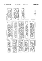
- FIG. 1a is simplified enlarged, cross-sectional view of an integrated LWIR/VIS/NIR imager that utilizes a silicon microbolometer cell (SMC) and current sampling readout and a CCD photogate and CCD column readout to achieve low noise operation;
- SMC silicon microbolometer cell
- FIG. 1b i is a more detailed cross-sectional view of the LWIR silicon microbolometer cell (SMC) of FIG. 1a;
- FIG. 1c is a top view of the SMC of FIG. 1b;
- FIG. 2 is an enlarged, cross-sectional view of an integrated LWIR/VIS/NIR imager that utilizes a CMOS column readout to achieve low noise operation;
- FIG. 3 is an enlarged, cross-sectional view of an integrated LWIR/VIS/NIR imager that employs optical enhancement using a microlens array that is optimized for high transmission and focusing both LWIR and VIS/NIR radiation within the sensor;
- FIG. 4a is an enlarged, cross-sectional view of an integrated imager that employs optical enhancement using a shaped reflective optical element as an optical concentrator;
- FIG. 4b illustrates an embodiment wherein the shaped reflector elements are incorporated into a vacuum lid of a package that encloses the imager;
- FIG. 5 is an enlarged, cross-sectional view of a three color LWIR/Visible/NIR imager, wherein color separation is achieved by selective etching of an atomically bonded NIR absorbing layer to provide an apertured layer;
- FIGS. 6a and 6b are plane and cross-sectional views, respectively, of the apertured LWIR/Visible/NIR imager of FIG. 5;
- FIG. 7 is an enlarged, cross-sectional view of a three color NWIR or LWIR/Visible/NIR imager having a 4:1 difference in resolution between the visible/NIR detectors and the MWIR or LWIR detector;
- FIGS. 8 and 9 are process flow diagrams that illustrate fabrication techniques for non-NIR and NIR responsive visible/LWIR sensor arrays, respectively.
- FIG. 1a illustrates a backside illuminated, CCD embodiment of a heterojunction bonded LWIR/VIS/NIR imager 10.
- the imager 10 includes a NIR-responsive detecting layer 12, a heterojunction atomic bonding layer or interface 14, and a silicon (or InP or GaAs) layer 16.
- the detecting layer 12 may be comprised of InP, GaAs or InGaAs.
- the detecting layer 12 may be comprised of HgCdTe.
- a suitable thickness for the detecting layer 12 is in the range of about one to ten micrometers, the actual thickness being a function at least in part of the IR wavelength band that is desired to be detected, while ten micrometers is a suitable thickness for the silicon layer 16.
- the NIR detecting layer may be provided on a surface of a transparent (at the wavelengths of interest) substrate, upon which the NIR detecting layer 12 has been previously epitaxially grown. The transparent substrate may be retained, or subsequently removed after the detecting layer 12 is atomically bonded to the silicon layer 16.
- NIR detecting layer 12 and atomic bonding interface 14
- atomic bonding interface 14 is optional (see, for example, FIGS. 3 and 4).
- the top surface 18 of the silicon layer 16, in this embodiment of this invention, is processed and patterned into a low noise CCD read-out structure and a bolometer readout (current or voltage mode).
- the CCD read-out structure includes photogate metalization 20a, under which charge carriers are collected, and transfer gate metalization 20b, which transfers the collected charge carriers to a column register 20c which then routes the collected charge to amplifying circuitry of known construction.
- Each photogate 20a can be considered to define one pixel or unit cell of the imager 10.
- FIG. 1a a buried channel (21) CCD implementation is depicted wherein photo-induced charge is transferred by applying a large positive potential to the transfer gate 20b for moving the charge from the photogate 20a to the receiving phase (electrode 20c) of the column CCD.
- the bolometer readout (current mode) employs a voltage bias and single switching transistor which when on enables current to flow from the bias supply through the bolometer and to be sampled and integrated by a column CTIA (capacitive transimpedance amplifier).
- Visible and IR radiation are incident on the backside of the imager 10 and pass substantially unabsorbed through the substrate (if present).
- NIR and visible radiation is absorbed in the narrower bandgap detecting layer 12.
- the LWIR (and/or MWIR) radiation is absorbed by a bolometer element 22 which is spaced away from the surface 18 by a thermal isolation bridge or spacer 22a.
- the bridge 22a may include a layer of thermal isolation material 24.
- the bolometer element 22 may be replaced by a pyroelectric element or by a thermopile element, or by any suitable thermal sensing element.
- Photoinduced charge carriers from the visible/NIR detecting layer 12 pass through the thin atomic bonding interface layer 14, and are swept by an electric field to respective ones of the photogates 20a for collection and integration. The collected charge is then subsequently transferred out of the photogates 20a by the associated transfer gates 20b.
- Gate 28a represents a current sampling disposed over a column output diffusion 28b. LWIR and/or MWIR radiation heats the thermally isolated thermal detector causing a change in its temperature. This temperature change in turn causes a change in the electrical characteristics of the sensing element; resistance, charge, or Seebeck voltage for bolometric, pyroelectric, and thermopile sensing elements, respectively.
- the change in the resistance is typically read as a change in the current for a constant voltage bias.
- This LWIR-induced current change can be read-out simultaneously with the charge from the photogate 20a, or sequentially therewith.
- the atomic bonding of the NIR detecting layer 12 is preferably accomplished after the processing of the low noise silicon circuits, i.e., CMOS or CCD, that are employed for collection, amplification and multiplexing of the photogenerated charge carriers.
- CMOS complementary metal-oxide-semiconductor
- CCD complementary metal-oxide-semiconductor
- the atomic bonding layer 14 enables the two dissimilar semiconductor material types (e.g., silicon and HgCdTe or InGaAs) to be physically and electrically coupled together, while compensating for lattice and energy bandgap mismatches between the two dissimilar semiconductor materials.
- the use of atomic bonding to join dissimilar semiconductor materials for constructing optical detectors and sources is known in the art, as evidenced by, for example, the following publications: L. H. Tan et al., "High quantum efficiency and narrow absorption bandwidth of the wafer-fused resonant In 0 .53 Ga 0 .47 As photodetectors", IEEE Photon. Technol. Lett., vol. 6, pp. 811-813, 1994; Z. L.
- any MWIR and LWIR radiation passes through the silicon layer 16 substantially unattenuated.
- the photogate 20a which collects photoelectrons generated by the visible and/or NIR radiation can be held at a DC bias, the polysilicon photogate doping is preferably adjusted so that free carrier absorption of the LWIR radiation is small (e.g., ⁇ 5%).
- the essentially unattenuated LWIR (or MWIR radiation) thus impinges on the thermal detecting material of element 22 (i.e., bolometer, pyroelectric or thermopile).
- a shaped reflector, as shown in FIGS. 4a, 4b, and 5, may be used to provide multiple passes of the LWIR while also concentrating the LWIR radiation onto the element 22.
- FIG. 1b illustrates, in cross-section, the LWIR silicon microbolometer cell (SMC) in greater detail, while FIG. 1c is a top view of same.
- Diffusion 28c is a voltage bias diffusion
- structures 29a and 29b a silicon nitride bridge and bridge legs, respectively
- the region 31 is region of undercut that provides a space (e.g., approximately 2-10 microns) beneath the bridge 29a and the overlying VO 2 microbolometer element 22, and metalization 33 provides low thermal conductivity SMC electrical contacts.
- the photogate 20a is shown disposed above an oxide layer 23b.
- FIG. 2 is similar to the embodiment of FIG. 1a, and illustrates an imager 10' implemented with low noise CMOS readout technology instead of the low noise CCD readout technology of FIG. 1.
- a visible/NIR column output diffusion 23 is located in the top surface 18 of the silicon layer 16, and the collected charge from the photogate 20a is transferred to the diffusion 23 by the transfer gate 20b resulting in a voltage change which can be optionally amplified within the unit cell and passed by a row address transistor to the column amplifier.
- the unit cell circuits depicted in Figs. 1a, 1b and 2 provide simultaneous or sequential readout of the thermal and visible/NIR detectors.
- Charge generated by the visible/NIR radiation is collected under the photogate 20a for the desired integration time, typically at video rates of 30 milliseconds or 60 milliseconds. After integration the charge is transferred to known types of external circuits for amplification, column readout, and serial multiplexing.
- CMOS amplifier within the unit cell (not shown) or to a column amplifier (not shown), such as a capacitive transimpedance amplifier (CTIA).
- CTIA capacitive transimpedance amplifier
- a low noise readout is obtained in this embodiment by several techniques. First, KTC noise is cancelled at the column by alternately reading the output amplifier after applying a reset signal, and before and after the photointegrated charge is transferred. Second, this embodiment makes use of low noise MOSFETs, buried channel FETS, and, where desired, JFETs, all constructed using conventional fabrication techniques.
- FIGS. 3, 4a and 4b illustrate optical enhancements to the imagers 10 and 10' of FIGS. 1 and 2, the optical enhancements being compatible with the low noise operation of these imagers.
- the enhancements enable collection of the majority of the photogenerated charge (i.e., photogenerated electrons (PE)) to be collected under the photogate 20a (visible sensor) or thermal radiation by the element 22 (IR sensor).
- PE photogenerated electrons
- FIG. 3 a microlens array 30, fabricated on a separate transparent substrate 32, is aligned to the imager chip and spaced apart from same by spacers 34 (such as indium columns).
- the microlens array 30 provides optical gain, focusing the incident radiation simultaneously on both the silicon layer 16 (visible focus (VF)) and the thermally isolated element 22 (IR focus (IRF)).
- the use of the microlens array 30 to implement an F2 system can enable gains in excess of four.
- the selection of material for the substrate 32 is important in order to attain a high transmission in both the visible and IR bands. Suitable materials for this purpose include, but are not limited to, ZnSe, ZnS, and CaF. It should be noted that the substrate 32 may actually be an entrance window of an enclosure or housing that contains the imager 10 or 10', along with related components, such as a thermoelectric (TE) cooler.
- TE thermoelectric
- microlens array 30 within the radiation receiving surface of the silicon layer 16, such as by photolithographically defining and then etching diffractive binary lens elements into the surface.
- a reflective microlens array formed on a dielectric substrate, is positioned over the top surface of the imager.
- dielectric or metallic spacers such as Indium
- the reflector is shaped for concentrating any IR radiation passing through or around a sensing element back onto the sensing element.
- an imager that is responsive to three separate bands of wavelengths, or "colors", can also be realized by the teachings of this invention.
- the backside, radiation-receiving surface of the imager is provided with a plurality of NIR absorbing layers 12 that are atomically bonded at heterojunction atomic bonding interfaces 14 to the silicon layer 16.
- the imager when viewed from the radiation receiving surface (FIG. 6a) the imager is seen as a checkerboard or strip pattern, with the LWIR/NIR-responsive unit cells alternating in a row/column manner with LWIR/VIS responsive unit cells.
- the NIR absorbing layer is selectively etched off the backside surface exposing the visible detection layer.
- Backside contact to both layers is made at the edges of the chip in the case of continuous rows (or columns), or through the deposition of a thin transparent conducting layer such as In-Sn oxide.
- a thin transparent conducting layer such as In-Sn oxide.
- the electric field lines sweep out charge generated only by the visible radiation, while in the regions where the NIR absorbing layer is present the photogenerated carriers from NIR and visible radiation are collected.
- charge carriers generated in the NIR (and visible) absorbing layers 12 are transported across the interface 14 and into the silicon layer 16 where they are collected beneath suitably biased photogates 20a.
- Those unit cells that do not include the NIR layer 12 admit visible light directly into the silicon layer 16.
- the charge carriers beneath the associated photogates 20a thus include photoelectrons that are generated within the In silicon layer 20 by the absorption of the visible light.
- the longer wavelength IR passes through the NIR layers 12 and the silicon layer 16, and may be focussed and detected as was described above with reference to FIG. 4. In this manner the NIR and visible components, with a LWIR (or MWIR) radiation component, can be spatially segregated and separately detected by the imager.
- the contribution of the visible radiation induced charge carriers can be removed, leaving only the contribution from the NIR radiation induced charge carriers.
- Alternative architectures improve the resolution in the visible, and provides multiple CCD pixels which collect electrons generated by visible radiation located within the extent of one larger pixel which responds to LWIR (or MWIR) radiation. This enables registration with but does not require oversampling of the LWIR signal.
- pixel sizes of the CCD may be as small as nine microns (center to center), whereas the LWIR blur size for 10 micron radiation with F1 optics is approximately 24 microns.
- a 4:1 ratio is shown, e.g., the CCD cell size is nine microns while the LWIR pixel size is 36 microns. Other ratios can be employed as desired.
- the single chip imager described above can be packaged in a low cost integrated vacuum housing and, as was also described above, a window of the housing may also provide pixel-based optical concentration, such as is shown in FIG. 3.
- Low cost temperature stabilization and cooling can be achieved using a single stage thermoelectric cooler operating from 250K to 300K.
- Imager formats exceeding 1000 ⁇ 1000 unit cells can be employed.
- a portion of the package can also be employed to support microreflectors.
- the construction of the imager 10 includes the doping of the silicon layer 16 and the doping and grading of the detecting layer 12 to facilitate charge transfer between these two layers at low illumination levels.
- the construction further includes the thinning of the silicon CCD layer 16, the bonding to the detecting layer 12 (in a hydrogen environment), and the final processing of the composite structure which can include photolithography and the etching of contacts, metallization, etc.
- FIG. 8 is a process flow diagram illustrating a method for fabricating a monolithic visible/LWIR bolometer sensor, without NIR capability.
- This method includes the following steps.
- Step A fabricate in a wafer (e.g., a standard Si 4" or 6" wafer) the CCD (or CMOS) readout circuits and gate structures using conventional metal, polysilicon and oxide layers and implantation.
- Step B fabricate the bolometer on the full thickness wafer, leaving the pixels unreleased.
- Step C mount the wafer front (WFR) surface on a temporary carrier and thin to a desired thickness.
- Step D produce an inverted lens array shape in the silicon surface.
- WFR wafer front
- Step E dope the wafer back-surface by ion implantation and low temperature annealing.
- Step F deposit cold (or hot) weld solder contacts (i.e. Indium) at the array edge.
- Step G fabricate the lens array in IR transparent material (i.e. ZnSe).
- Step H pattern the lens array with solder cold or hot weld contacts (i.e. Indium).
- Step I align and hybridize the ZnSe lens array to the silicon array, bringing the two surfaces into intimate contact and thus providing the wfr carrier.
- Step J the temporary carrier is removed, and the bolometer pixels are released (i.e., etching out the support structure such that the bolometer, resting on the thin nitride layer (bridge 29a) is supported by the (two) bridge legs 29b).
- FIG. 9 is a process flow diagram illustrating a method for fabricating a monolithic visible/LWIR sensor (employing ZnSe), with NIR capability.
- This method includes the following steps.
- Step A fabricate the CCD or CMOS readout circuits on a full thickness silicon wafer.
- Step B mount the front side of the wafer onto a temporary carrier and thin the silicon back side to the desired thickness.
- Step C contact bond the back side of the wafer to an InGaAs layer that has been grown on an InP substrate.
- Step D remove the temporary carrier and complete the wafer fusing process.
- Step E fabricate the bolometer layers on the front side, up to the pixel release step.
- Step F mount the front side onto a temporary carrier; selectively remove the InP substrate from the back side, and selectively remove the NIR layer as required (see, for example FIGS. 6a and 6b.
- Step G deposit cold or hot weld solder contacts (i.e. Indium) at the array edge.
- Step H pattern an IR transparent substrate, such as ZnSe, with matching cold or hot weld contacts and hybridize to the back side so as to bring the two surfaces into intimate contact.
- Step I remove the temporary carrier from the front side.
- Step J fabricate one or more reflector arrays using the same microlens fabrication technique (i.e. photosculpture) in a Si (or other) substrate.
- Step K deposit cold or hot weld solder contacts (i.e. Indium) at the edge of the reflector array.
- Step L align/hybridize the reflector array to the sensor array front, thereby providing a proximity reflector.
- Step M release the bolometer pixels.
- the thinned silicon layer 16 is bonded to the detecting layer 12 in an H 2 or Hg atmosphere (or in vacuum) by the application of pressure at a temperature greater than >400 C to effect chemical bonding.
- a H 2 atmosphere may be desirable for use when bonding an InGaAs layer 12 to the silicon layer 16.
- the imager 10 may be operated as an Avalanche Photodiode Imager (API) wherein amplification of the charge carrier signal is achieved through avalanche multiplication.
- API Avalanche Photodiode Imager
- An electric field strength in excess of 200 kV/cm is believed to be adequate to achieve the avalanche multiplication effect in the silicon layer 16.
- a low noise avalanche gain (excess noise factor, F ⁇ 4) can thus be achieved.
- Group IV materials such as germanium or germanium/silicon alloys
- Group IV-VI materials such as Pb-salt semiconductors, e.g., PbSe, PbS, PbTe, etc.
- PbSe, PbS, PbTe, etc. can also be employed.
Abstract
Description
Claims (29)
Priority Applications (1)
| Application Number | Priority Date | Filing Date | Title |
|---|---|---|---|
| US08/778,934 US5808350A (en) | 1997-01-03 | 1997-01-03 | Integrated IR, visible and NIR sensor and methods of fabricating same |
Applications Claiming Priority (1)
| Application Number | Priority Date | Filing Date | Title |
|---|---|---|---|
| US08/778,934 US5808350A (en) | 1997-01-03 | 1997-01-03 | Integrated IR, visible and NIR sensor and methods of fabricating same |
Publications (1)
| Publication Number | Publication Date |
|---|---|
| US5808350A true US5808350A (en) | 1998-09-15 |
Family
ID=25114807
Family Applications (1)
| Application Number | Title | Priority Date | Filing Date |
|---|---|---|---|
| US08/778,934 Expired - Fee Related US5808350A (en) | 1997-01-03 | 1997-01-03 | Integrated IR, visible and NIR sensor and methods of fabricating same |
Country Status (1)
| Country | Link |
|---|---|
| US (1) | US5808350A (en) |
Cited By (148)
| Publication number | Priority date | Publication date | Assignee | Title |
|---|---|---|---|---|
| EP1022551A2 (en) * | 1999-01-12 | 2000-07-26 | Nec Corporation | Thermal infrared array sensor for detecting a plurality of infrared wavelength bands |
| WO2001009579A1 (en) * | 1999-07-30 | 2001-02-08 | Xactix, Inc. | Thermal isolation using vertical structures |
| US6232602B1 (en) | 1999-03-05 | 2001-05-15 | Flir Systems, Inc. | Enhanced vision system sensitive to infrared radiation |
| US6242740B1 (en) * | 1997-09-16 | 2001-06-05 | Metorex International Oy | Imaging system functioning on submillimeter waves |
| US6307194B1 (en) | 1999-06-07 | 2001-10-23 | The Boeing Company | Pixel structure having a bolometer with spaced apart absorber and transducer layers and an associated fabrication method |
| US6313457B1 (en) | 1999-01-25 | 2001-11-06 | Gentex Corporation | Moisture detecting system using semiconductor light sensor with integral charge collection |
| US20020030163A1 (en) * | 2000-08-09 | 2002-03-14 | Zhang Evan Y.W. | Image intensifier and LWIR fusion/combination system |
| US6359274B1 (en) | 1999-01-25 | 2002-03-19 | Gentex Corporation | Photodiode light sensor |
| US6379013B1 (en) | 1999-01-25 | 2002-04-30 | Gentex Corporation | Vehicle equipment control with semiconductor light sensors |
| WO2002037146A1 (en) * | 2000-11-03 | 2002-05-10 | Mems Optical Inc. | Anti-reflective structures |
| US6392234B2 (en) * | 1998-08-05 | 2002-05-21 | Drager Sicherheitstechnik Gmbh | Infrared optical gas sensor |
| US6402328B1 (en) | 1999-01-25 | 2002-06-11 | Gentex Corporation | Automatic dimming mirror using semiconductor light sensor with integral charge collection |
| EP1215729A2 (en) * | 2000-12-18 | 2002-06-19 | Canon Kabushiki Kaisha | Image pickup apparatus |
| US6433326B1 (en) | 1999-07-14 | 2002-08-13 | Sarnoff Corporation | CMOS/CCD line transfer imager with low dark current |
| US20030001093A1 (en) * | 2001-06-27 | 2003-01-02 | Honeywell Inc. | Sensor for dual wavelength bands |
| US6561693B1 (en) * | 2000-09-21 | 2003-05-13 | Lockheed Martin Corporation | Remote temperature sensing long wave length modulated focal plane array |
| US20030123159A1 (en) * | 2001-03-09 | 2003-07-03 | Masayuki Morita | Diffraction lens element and lighting system using the lens element |
| US6638837B1 (en) * | 2002-09-20 | 2003-10-28 | Taiwan Semiconductor Manufacturing Company | Method for protecting the front side of semiconductor wafers |
| US6646799B1 (en) | 2000-08-30 | 2003-11-11 | Science Applications International Corporation | System and method for combining multiple energy bands to improve scene viewing |
| US20040005086A1 (en) * | 2002-07-03 | 2004-01-08 | Equinox Corporation | Method and apparatus for using thermal infrared for face recognition |
| US6709985B1 (en) * | 1999-08-26 | 2004-03-23 | Advanced Micro Devices, Inc. | Arrangement and method for providing an imaging path using a silicon-crystal damaging laser |
| US20040140429A1 (en) * | 2002-12-02 | 2004-07-22 | Raytheon Company | Passive millimeter wave sensor using high temperature superconducting leads |
| US6781127B1 (en) | 2000-06-08 | 2004-08-24 | Equinox Corporation | Common aperture fused reflective/thermal emitted sensor and system |
| US6811085B2 (en) * | 2001-10-26 | 2004-11-02 | Symbol Technologies, Inc. | Miniature imager |
| US20050024729A1 (en) * | 2002-01-10 | 2005-02-03 | Ockerse Harold C. | Dimmable rearview assembly having a glare sensor |
| US6872992B2 (en) * | 1999-04-13 | 2005-03-29 | Hamamatsu Photonics K.K. | Semiconductor device for detecting wide wavelength ranges |
| WO2005094460A3 (en) * | 2004-03-23 | 2005-12-29 | Bae Systems Information | Multi-spectral uncooled microbolometer detectors |
| EP1612528A2 (en) * | 2004-06-24 | 2006-01-04 | Robert Bosch Gmbh | Microstructured infrared sensor and process for its manufacture |
| US7084010B1 (en) | 2003-10-17 | 2006-08-01 | Raytheon Company | Integrated package design and method for a radiation sensing device |
| US7105821B1 (en) | 2003-12-15 | 2006-09-12 | Raytheon Company | Thermally stabilized radiation detector utilizing temperature controlled radiation filter |
| US20060249679A1 (en) * | 2004-12-03 | 2006-11-09 | Johnson Kirk R | Visible light and ir combined image camera |
| WO2006122529A2 (en) * | 2005-05-17 | 2006-11-23 | Heimann Sensor Gmbh | Thermopile infrared sensor array |
| US20060274431A1 (en) * | 2005-06-07 | 2006-12-07 | Honeywell International Inc. | Multi-band lens |
| US20070040119A1 (en) * | 2005-08-16 | 2007-02-22 | Institut National D'optique | Fast microbolometer pixels with integrated micro-optical focusing elements |
| US20070259463A1 (en) * | 2006-05-02 | 2007-11-08 | Youssef Abedini | Wafer-level method for thinning imaging sensors for backside illumination |
| US20080068478A1 (en) * | 2006-09-14 | 2008-03-20 | Fujifilm Corporation | Image sensor and digital camera |
| US20080093554A1 (en) * | 2006-10-24 | 2008-04-24 | Raytheon Company | Dual band imager with visible or SWIR detectors combined with uncooled LWIR detectors |
| US20080099678A1 (en) * | 2004-12-03 | 2008-05-01 | Johnson Kirk R | Camera with visible light and infrared image blending |
| WO2009013418A1 (en) * | 2007-07-26 | 2009-01-29 | Commissariat A L'energie Atomique | Bispectral detection device and bispectral detector including such device |
| US20090050806A1 (en) * | 2004-12-03 | 2009-02-26 | Fluke Corporation | Visible light and ir combined image camera with a laser pointer |
| US20090050947A1 (en) * | 2007-08-24 | 2009-02-26 | Micron Technology, Inc. | Apparatus, system, and method providing backside illuminated imaging device |
| US20090152475A1 (en) * | 2006-01-20 | 2009-06-18 | Sumitomo Electric Industries, Ltd. | Analyzer, Authenticity Judging Device, Authenticity Judging Method, and Underground Searching Method |
| US20090284404A1 (en) * | 2008-05-14 | 2009-11-19 | Electronics And Telecommunications Research Institute | Electromagnetic wave absorber using resistive material |
| WO2009151903A2 (en) * | 2008-05-20 | 2009-12-17 | Pelican Imaging Corporation | Capturing and processing of images using monolithic camera array with hetergeneous imagers |
| US20100123504A1 (en) * | 2008-11-14 | 2010-05-20 | Lauxtermann Stefan C | Adaptive low noise offset subtraction for imagers with long integration times |
| US20100156695A1 (en) * | 2008-12-22 | 2010-06-24 | Dong-Uk Sim | Electromagnetic absorber using resistive material |
| FR2941329A1 (en) * | 2009-01-19 | 2010-07-23 | Ulis | Visible/infrared radiation detector for e.g. monitoring field, has control circuit to control connection of units to control simultaneous integration of currents from pixels and maintenance of charges stored in units till end of integration |
| US20100187580A1 (en) * | 2008-07-28 | 2010-07-29 | Yang Xiao Charles | Method and structure of monolithically integrated infrared sensing device |
| US20110057285A1 (en) * | 2009-09-10 | 2011-03-10 | Thorsten Mueller | Sensor for detecting thermal radiation |
| US20110147573A1 (en) * | 2007-08-20 | 2011-06-23 | Perkinelmer Optoelectronics Gmbh & Co. Kg | Sensor cap assembly sensor circuit |
| WO2011129856A2 (en) | 2010-02-02 | 2011-10-20 | Raytheon Company | Transparent silicon detector and multimode seeker using the detector |
| US20110266443A1 (en) * | 2010-04-28 | 2011-11-03 | Schimert Thomas R | Pixel-level optical elements for uncooled infrared detector devices |
| FR2966977A1 (en) * | 2010-11-03 | 2012-05-04 | Commissariat Energie Atomique | VISIBLE AND NEAR INFRARED RADIATION DETECTOR |
| WO2012059656A1 (en) | 2010-11-03 | 2012-05-10 | Commissariat A L'energie Atomique Et Aux Energies Alternatives | Visible and near-infrared radiation detector |
| US20120161001A1 (en) * | 2010-12-23 | 2012-06-28 | Flir Systems, Inc. | Monolithic electro-optical polymer infrared focal plane array |
| WO2012121526A3 (en) * | 2011-03-04 | 2012-12-27 | 한국과학기술원 | Infrared sensor chip, infrared detector and an operating method and test method therefor |
| WO2013064753A1 (en) | 2010-11-03 | 2013-05-10 | Commissariat A L'energie Atomique Et Aux Energies Alternatives | Monolithic multispectral visible-and-infrared imager |
| US20130206990A1 (en) * | 2011-08-22 | 2013-08-15 | ISC8 Inc. | Background Limited Focal Plane Array Assembly |
| US8514491B2 (en) | 2009-11-20 | 2013-08-20 | Pelican Imaging Corporation | Capturing and processing of images using monolithic camera array with heterogeneous imagers |
| US8513605B2 (en) | 2010-04-28 | 2013-08-20 | L-3 Communications Corporation | Optically transitioning thermal detector structures |
| US8620523B2 (en) | 2011-06-24 | 2013-12-31 | Gentex Corporation | Rearview assembly with multiple ambient light sensors |
| US8619082B1 (en) | 2012-08-21 | 2013-12-31 | Pelican Imaging Corporation | Systems and methods for parallax detection and correction in images captured using array cameras that contain occlusions using subsets of images to perform depth estimation |
| US8692893B2 (en) | 2011-05-11 | 2014-04-08 | Pelican Imaging Corporation | Systems and methods for transmitting and receiving array camera image data |
| US8704238B2 (en) | 2008-07-08 | 2014-04-22 | MCube Inc. | Method and structure of monolithically integrated IC-MEMS oscillator using IC foundry-compatible processes |
| US8804255B2 (en) | 2011-06-28 | 2014-08-12 | Pelican Imaging Corporation | Optical arrangements for use with an array camera |
| US8831367B2 (en) | 2011-09-28 | 2014-09-09 | Pelican Imaging Corporation | Systems and methods for decoding light field image files |
| US8866912B2 (en) | 2013-03-10 | 2014-10-21 | Pelican Imaging Corporation | System and methods for calibration of an array camera using a single captured image |
| US8866920B2 (en) | 2008-05-20 | 2014-10-21 | Pelican Imaging Corporation | Capturing and processing of images using monolithic camera array with heterogeneous imagers |
| US8878950B2 (en) | 2010-12-14 | 2014-11-04 | Pelican Imaging Corporation | Systems and methods for synthesizing high resolution images using super-resolution processes |
| FR3005367A1 (en) * | 2013-05-06 | 2014-11-07 | Vence Innovation | COMPACT DETECTOR OF HUMAN PRESENCE |
| US20140332665A1 (en) * | 2010-04-21 | 2014-11-13 | Sionyx, Inc. | Photosensitive imaging devices and associated methods |
| US8928793B2 (en) | 2010-05-12 | 2015-01-06 | Pelican Imaging Corporation | Imager array interfaces |
| US8937361B2 (en) | 2011-02-03 | 2015-01-20 | Digitaloptics Corporation | BSI image sensor package with variable-height silicon for even reception of different wavelengths |
| US8999835B2 (en) | 2008-07-28 | 2015-04-07 | MCube Inc. | Method and structure of monolithically integrated ESD supperssion device |
| US9041133B2 (en) | 2011-02-03 | 2015-05-26 | Nan Chang O-Film Optoelectronics Technology Ltd | BSI image sensor package with embedded absorber for even reception of different wavelengths |
| US20150171234A1 (en) * | 2013-12-12 | 2015-06-18 | Raytheon Company | Broadband graphene-based optical limiter for the protection of backside illuminated cmos detectors |
| US9100635B2 (en) | 2012-06-28 | 2015-08-04 | Pelican Imaging Corporation | Systems and methods for detecting defective camera arrays and optic arrays |
| US9100586B2 (en) | 2013-03-14 | 2015-08-04 | Pelican Imaging Corporation | Systems and methods for photometric normalization in array cameras |
| US9106784B2 (en) | 2013-03-13 | 2015-08-11 | Pelican Imaging Corporation | Systems and methods for controlling aliasing in images captured by an array camera for use in super-resolution processing |
| US9124831B2 (en) | 2013-03-13 | 2015-09-01 | Pelican Imaging Corporation | System and methods for calibration of an array camera |
| US9143711B2 (en) | 2012-11-13 | 2015-09-22 | Pelican Imaging Corporation | Systems and methods for array camera focal plane control |
| US9185276B2 (en) | 2013-11-07 | 2015-11-10 | Pelican Imaging Corporation | Methods of manufacturing array camera modules incorporating independently aligned lens stacks |
| US9210392B2 (en) | 2012-05-01 | 2015-12-08 | Pelican Imaging Coporation | Camera modules patterned with pi filter groups |
| US9207116B2 (en) | 2013-02-12 | 2015-12-08 | Gentex Corporation | Light sensor |
| US9214013B2 (en) | 2012-09-14 | 2015-12-15 | Pelican Imaging Corporation | Systems and methods for correcting user identified artifacts in light field images |
| US9224889B2 (en) | 2011-08-05 | 2015-12-29 | Gentex Corporation | Optical assembly for a light sensor, light sensor assembly using the optical assembly, and vehicle rearview assembly using the light sensor assembly |
| US9247117B2 (en) | 2014-04-07 | 2016-01-26 | Pelican Imaging Corporation | Systems and methods for correcting for warpage of a sensor array in an array camera module by introducing warpage into a focal plane of a lens stack array |
| US9253380B2 (en) | 2013-02-24 | 2016-02-02 | Pelican Imaging Corporation | Thin form factor computational array cameras and modular array cameras |
| US9373733B2 (en) * | 2014-06-16 | 2016-06-21 | Sumitomo Electric Industries, Ltd. | Semiconductor light-receiving device and semiconductor light-receiving device array |
| EP1963798A4 (en) * | 2005-12-21 | 2016-06-22 | Searete Llc | Multi-stage waveform detector |
| US9412206B2 (en) | 2012-02-21 | 2016-08-09 | Pelican Imaging Corporation | Systems and methods for the manipulation of captured light field image data |
| US9426361B2 (en) | 2013-11-26 | 2016-08-23 | Pelican Imaging Corporation | Array camera configurations incorporating multiple constituent array cameras |
| US9438888B2 (en) | 2013-03-15 | 2016-09-06 | Pelican Imaging Corporation | Systems and methods for stereo imaging with camera arrays |
| US9445003B1 (en) | 2013-03-15 | 2016-09-13 | Pelican Imaging Corporation | Systems and methods for synthesizing high resolution images using image deconvolution based on motion and depth information |
| US9462164B2 (en) | 2013-02-21 | 2016-10-04 | Pelican Imaging Corporation | Systems and methods for generating compressed light field representation data using captured light fields, array geometry, and parallax information |
| US9496308B2 (en) | 2011-06-09 | 2016-11-15 | Sionyx, Llc | Process module for increasing the response of backside illuminated photosensitive imagers and associated methods |
| US9497429B2 (en) | 2013-03-15 | 2016-11-15 | Pelican Imaging Corporation | Extended color processing on pelican array cameras |
| US9497370B2 (en) | 2013-03-15 | 2016-11-15 | Pelican Imaging Corporation | Array camera architecture implementing quantum dot color filters |
| US9516222B2 (en) | 2011-06-28 | 2016-12-06 | Kip Peli P1 Lp | Array cameras incorporating monolithic array camera modules with high MTF lens stacks for capture of images used in super-resolution processing |
| US9521319B2 (en) | 2014-06-18 | 2016-12-13 | Pelican Imaging Corporation | Array cameras and array camera modules including spectral filters disposed outside of a constituent image sensor |
| US9521416B1 (en) | 2013-03-11 | 2016-12-13 | Kip Peli P1 Lp | Systems and methods for image data compression |
| US9519972B2 (en) | 2013-03-13 | 2016-12-13 | Kip Peli P1 Lp | Systems and methods for synthesizing images from image data captured by an array camera using restricted depth of field depth maps in which depth estimation precision varies |
| US9536917B2 (en) * | 2013-11-19 | 2017-01-03 | Raytheon Company | Two color detector leveraging resonant cavity enhancement for performance improvement |
| US9578259B2 (en) | 2013-03-14 | 2017-02-21 | Fotonation Cayman Limited | Systems and methods for reducing motion blur in images or video in ultra low light with array cameras |
| US9595479B2 (en) | 2008-07-08 | 2017-03-14 | MCube Inc. | Method and structure of three dimensional CMOS transistors with hybrid crystal orientations |
| US9635287B2 (en) | 2011-10-11 | 2017-04-25 | Raytheon Company | Method and apparatus for integrated sensor to provide higher resolution, lower frame rate and lower resolution, higher frame rate imagery simultaneously |
| US9633442B2 (en) | 2013-03-15 | 2017-04-25 | Fotonation Cayman Limited | Array cameras including an array camera module augmented with a separate camera |
| US9638883B1 (en) | 2013-03-04 | 2017-05-02 | Fotonation Cayman Limited | Passive alignment of array camera modules constructed from lens stack arrays and sensors based upon alignment information obtained during manufacture of array camera modules using an active alignment process |
| US9673250B2 (en) | 2013-06-29 | 2017-06-06 | Sionyx, Llc | Shallow trench textured regions and associated methods |
| US9673243B2 (en) | 2009-09-17 | 2017-06-06 | Sionyx, Llc | Photosensitive imaging devices and associated methods |
| US9761739B2 (en) | 2010-06-18 | 2017-09-12 | Sionyx, Llc | High speed photosensitive devices and associated methods |
| US9762830B2 (en) | 2013-02-15 | 2017-09-12 | Sionyx, Llc | High dynamic range CMOS image sensor having anti-blooming properties and associated methods |
| US9766380B2 (en) | 2012-06-30 | 2017-09-19 | Fotonation Cayman Limited | Systems and methods for manufacturing camera modules using active alignment of lens stack arrays and sensors |
| US9774789B2 (en) | 2013-03-08 | 2017-09-26 | Fotonation Cayman Limited | Systems and methods for high dynamic range imaging using array cameras |
| US9794476B2 (en) | 2011-09-19 | 2017-10-17 | Fotonation Cayman Limited | Systems and methods for controlling aliasing in images captured by an array camera for use in super resolution processing using pixel apertures |
| US9813616B2 (en) | 2012-08-23 | 2017-11-07 | Fotonation Cayman Limited | Feature based high resolution motion estimation from low resolution images captured using an array source |
| US9870753B2 (en) | 2013-02-12 | 2018-01-16 | Gentex Corporation | Light sensor having partially opaque optic |
| US9881966B2 (en) * | 2015-07-17 | 2018-01-30 | International Business Machines Corporation | Three-dimensional integrated multispectral imaging sensor |
| US9888194B2 (en) | 2013-03-13 | 2018-02-06 | Fotonation Cayman Limited | Array camera architecture implementing quantum film image sensors |
| US9898856B2 (en) | 2013-09-27 | 2018-02-20 | Fotonation Cayman Limited | Systems and methods for depth-assisted perspective distortion correction |
| US9905599B2 (en) | 2012-03-22 | 2018-02-27 | Sionyx, Llc | Pixel isolation elements, devices and associated methods |
| US9911781B2 (en) | 2009-09-17 | 2018-03-06 | Sionyx, Llc | Photosensitive imaging devices and associated methods |
| US9939251B2 (en) | 2013-03-15 | 2018-04-10 | Sionyx, Llc | Three dimensional imaging utilizing stacked imager devices and associated methods |
| US9942474B2 (en) | 2015-04-17 | 2018-04-10 | Fotonation Cayman Limited | Systems and methods for performing high speed video capture and depth estimation using array cameras |
| US10044922B1 (en) | 2017-07-06 | 2018-08-07 | Arraiy, Inc. | Hardware system for inverse graphics capture |
| US10089740B2 (en) | 2014-03-07 | 2018-10-02 | Fotonation Limited | System and methods for depth regularization and semiautomatic interactive matting using RGB-D images |
| US10122993B2 (en) | 2013-03-15 | 2018-11-06 | Fotonation Limited | Autofocus system for a conventional camera that uses depth information from an array camera |
| US10119808B2 (en) | 2013-11-18 | 2018-11-06 | Fotonation Limited | Systems and methods for estimating depth from projected texture using camera arrays |
| US10244188B2 (en) | 2011-07-13 | 2019-03-26 | Sionyx, Llc | Biometric imaging devices and associated methods |
| US10250871B2 (en) | 2014-09-29 | 2019-04-02 | Fotonation Limited | Systems and methods for dynamic calibration of array cameras |
| US10361083B2 (en) | 2004-09-24 | 2019-07-23 | President And Fellows Of Harvard College | Femtosecond laser-induced formation of submicrometer spikes on a semiconductor substrate |
| US10374109B2 (en) | 2001-05-25 | 2019-08-06 | President And Fellows Of Harvard College | Silicon-based visible and near-infrared optoelectric devices |
| US10390005B2 (en) | 2012-09-28 | 2019-08-20 | Fotonation Limited | Generating images from light fields utilizing virtual viewpoints |
| US10482618B2 (en) | 2017-08-21 | 2019-11-19 | Fotonation Limited | Systems and methods for hybrid depth regularization |
| WO2020074785A1 (en) * | 2018-10-11 | 2020-04-16 | Emberion Oy | Multispectral photodetector array |
| US10666929B2 (en) | 2017-07-06 | 2020-05-26 | Matterport, Inc. | Hardware system for inverse graphics capture |
| US11270110B2 (en) | 2019-09-17 | 2022-03-08 | Boston Polarimetrics, Inc. | Systems and methods for surface modeling using polarization cues |
| US11290658B1 (en) | 2021-04-15 | 2022-03-29 | Boston Polarimetrics, Inc. | Systems and methods for camera exposure control |
| US11302012B2 (en) | 2019-11-30 | 2022-04-12 | Boston Polarimetrics, Inc. | Systems and methods for transparent object segmentation using polarization cues |
| US20220214223A1 (en) * | 2019-05-21 | 2022-07-07 | Nextinput, Inc. | Combined near and mid infrared sensor in a chip scale package |
| US11496697B2 (en) | 2020-02-28 | 2022-11-08 | Samsung Electronics Co., Ltd. | LWIR sensor with capacitive microbolometer and hybrid visible/LWIR sensor |
| US11525906B2 (en) | 2019-10-07 | 2022-12-13 | Intrinsic Innovation Llc | Systems and methods for augmentation of sensor systems and imaging systems with polarization |
| US11580667B2 (en) | 2020-01-29 | 2023-02-14 | Intrinsic Innovation Llc | Systems and methods for characterizing object pose detection and measurement systems |
| US11689813B2 (en) | 2021-07-01 | 2023-06-27 | Intrinsic Innovation Llc | Systems and methods for high dynamic range imaging using crossed polarizers |
| US11792538B2 (en) | 2008-05-20 | 2023-10-17 | Adeia Imaging Llc | Capturing and processing of images including occlusions focused on an image sensor by a lens stack array |
| US11797863B2 (en) | 2020-01-30 | 2023-10-24 | Intrinsic Innovation Llc | Systems and methods for synthesizing data for training statistical models on different imaging modalities including polarized images |
| US11954886B2 (en) | 2021-04-15 | 2024-04-09 | Intrinsic Innovation Llc | Systems and methods for six-degree of freedom pose estimation of deformable objects |
| US11953700B2 (en) | 2020-05-27 | 2024-04-09 | Intrinsic Innovation Llc | Multi-aperture polarization optical systems using beam splitters |
Citations (8)
| Publication number | Priority date | Publication date | Assignee | Title |
|---|---|---|---|---|
| US4213137A (en) * | 1976-11-16 | 1980-07-15 | Hughes Aircraft Company | Monolithic variable size detector |
| US4257057A (en) * | 1979-05-07 | 1981-03-17 | Rockwell International Corporation | Self-multiplexed monolithic intrinsic infrared detector |
| US4258376A (en) * | 1976-03-30 | 1981-03-24 | U.S. Philips Corporation | Charge coupled circuit arrangement using a punch-through charge introduction effect |
| US4626675A (en) * | 1982-02-22 | 1986-12-02 | International Standard Electric Corporation | Demultiplexing photodiode sensitive to plural wavelength bands |
| US5373182A (en) * | 1993-01-12 | 1994-12-13 | Santa Barbara Research Center | Integrated IR and visible detector |
| US5432374A (en) * | 1993-02-08 | 1995-07-11 | Santa Barbara Research Center | Integrated IR and mm-wave detector |
| US5559336A (en) * | 1994-07-05 | 1996-09-24 | Santa Barbara Research Center | Integrated LPE-grown structure for simultaneous detection of infrared radiation in two bands |
| US5567975A (en) * | 1994-06-30 | 1996-10-22 | Santa Barbara Research Center | Group II-VI radiation detector for simultaneous visible and IR detection |
-
1997
- 1997-01-03 US US08/778,934 patent/US5808350A/en not_active Expired - Fee Related
Patent Citations (8)
| Publication number | Priority date | Publication date | Assignee | Title |
|---|---|---|---|---|
| US4258376A (en) * | 1976-03-30 | 1981-03-24 | U.S. Philips Corporation | Charge coupled circuit arrangement using a punch-through charge introduction effect |
| US4213137A (en) * | 1976-11-16 | 1980-07-15 | Hughes Aircraft Company | Monolithic variable size detector |
| US4257057A (en) * | 1979-05-07 | 1981-03-17 | Rockwell International Corporation | Self-multiplexed monolithic intrinsic infrared detector |
| US4626675A (en) * | 1982-02-22 | 1986-12-02 | International Standard Electric Corporation | Demultiplexing photodiode sensitive to plural wavelength bands |
| US5373182A (en) * | 1993-01-12 | 1994-12-13 | Santa Barbara Research Center | Integrated IR and visible detector |
| US5432374A (en) * | 1993-02-08 | 1995-07-11 | Santa Barbara Research Center | Integrated IR and mm-wave detector |
| US5567975A (en) * | 1994-06-30 | 1996-10-22 | Santa Barbara Research Center | Group II-VI radiation detector for simultaneous visible and IR detection |
| US5559336A (en) * | 1994-07-05 | 1996-09-24 | Santa Barbara Research Center | Integrated LPE-grown structure for simultaneous detection of infrared radiation in two bands |
Non-Patent Citations (14)
| Title |
|---|
| "Analysis of wafer fusing for 1.3pm vertical cavity surface emitting lasers", R.J. Ram et al, Appl. Phys. Lett. 62, May 17, 1993, pp. 2474-2476. |
| "High Quantum Efficiency and Narrow Absorption Bandwidth of the Wafer-Fused Resonant In0.53 Ga0.47 As Photodetectors", I-Hsing Tan et al., IEEE Photonics Technology Letters, vol. 6, No. 7, Jul. 1994. |
| "Low threshold, wafer fused long wavelength vertical cavity lasers", J. J. Dudley et al.,Appl. Phys. Lett. 64, Mar. 21, 1994, pp. 1463-1465. |
| Analysis of wafer fusing for 1.3pm vertical cavity surface emitting lasers , R.J. Ram et al, Appl. Phys. Lett. 62, May 17, 1993, pp. 2474 2476. * |
| Electrical characteristics of directly bonded GaAs and InP, Hiroshi Wada et al., Appl. Phys. Lett. 62, Feb. 15, 1993, pp. 738 740. * |
| Electrical characteristics of directly-bonded GaAs and InP, Hiroshi Wada et al., Appl. Phys. Lett. 62, Feb. 15, 1993, pp. 738-740. |
| High Quantum Efficiency and Narrow Absorption Bandwidth of the Wafer Fused Resonant In 0.53 Ga 0.47 As Photodetectors , I Hsing Tan et al., IEEE Photonics Technology Letters, vol. 6, No. 7, Jul. 1994. * |
| Leos 95, IEEE Lasers and Electro Optics Society 1995 Annual Meeting, 8th Annual Meeting, Conference Proceedings (Cat. No. 95CH35739) Part vol. 1, pp. 29 30 vol. 1. * |
| Leos '95, IEEE Lasers and Electro-Optics Society 1995 Annual Meeting, 8th Annual Meeting, Conference Proceedings (Cat. No. 95CH35739) Part vol. 1, pp. 29-30 vol. 1. |
| Low threshold, wafer fused long wavelength vertical cavity lasers , J. J. Dudley et al.,Appl. Phys. Lett. 64, Mar. 21, 1994, pp. 1463 1465. * |
| Modeling and Performance of Wafer Fused Resonant Cavity Enhanced Photodetectors, I Hsing Tan et al. IEEE Journal of Quantum Electronics, vol. 31, No. 10, Oct. 1995. * |
| Modeling and Performance of Wafer-Fused Resonant-Cavity Enhanced Photodetectors, I-Hsing Tan et al. IEEE Journal of Quantum Electronics, vol. 31, No. 10, Oct. 1995. |
| Wafer fusion: A novel technique for optoelectronic device fabrication and monolithic integration, Z. L. Liau et al., Appl. Phys. Lett. 56, Feb. 19, 1990, pp. 737 739. * |
| Wafer fusion: A novel technique for optoelectronic device fabrication and monolithic integration, Z. L. Liau et al., Appl. Phys. Lett. 56, Feb. 19, 1990, pp. 737-739. |
Cited By (378)
| Publication number | Priority date | Publication date | Assignee | Title |
|---|---|---|---|---|
| US6242740B1 (en) * | 1997-09-16 | 2001-06-05 | Metorex International Oy | Imaging system functioning on submillimeter waves |
| US6392234B2 (en) * | 1998-08-05 | 2002-05-21 | Drager Sicherheitstechnik Gmbh | Infrared optical gas sensor |
| EP1022551A3 (en) * | 1999-01-12 | 2004-03-17 | Nec Corporation | Thermal infrared array sensor for detecting a plurality of infrared wavelength bands |
| EP1022551A2 (en) * | 1999-01-12 | 2000-07-26 | Nec Corporation | Thermal infrared array sensor for detecting a plurality of infrared wavelength bands |
| US7378633B2 (en) | 1999-01-25 | 2008-05-27 | Gentex Corporation | Vehicle rearview assembly having a light sensor with two or more transducers |
| US20060268416A1 (en) * | 1999-01-25 | 2006-11-30 | Nixon Robert H | Light Sensor |
| US7361875B2 (en) | 1999-01-25 | 2008-04-22 | Gentex Corporation | Vehicle headlamp control utilizing a light sensor having at least two light transducers |
| US6359274B1 (en) | 1999-01-25 | 2002-03-19 | Gentex Corporation | Photodiode light sensor |
| US20040218277A1 (en) * | 1999-01-25 | 2004-11-04 | Bechtel Jon H. | Automatic dimming mirror using semiconductor glare sensor |
| US6379013B1 (en) | 1999-01-25 | 2002-04-30 | Gentex Corporation | Vehicle equipment control with semiconductor light sensors |
| US20040222359A1 (en) * | 1999-01-25 | 2004-11-11 | Nixon Robert H. | Light sensor |
| US6755542B2 (en) | 1999-01-25 | 2004-06-29 | Gentex Corporation | Automatic dimming mirror using semiconductor light sensor with integral charge collection |
| US6402328B1 (en) | 1999-01-25 | 2002-06-11 | Gentex Corporation | Automatic dimming mirror using semiconductor light sensor with integral charge collection |
| US7087878B2 (en) | 1999-01-25 | 2006-08-08 | Gentex Corporation | Rearview assembly for a vehicle including a light sensor having first and second light transducers that are not exposed to the same optical spectrum |
| US20020093741A1 (en) * | 1999-01-25 | 2002-07-18 | Bechtel Jon H. | Vehicle equipment control with semiconductor light sensors |
| US6863405B2 (en) | 1999-01-25 | 2005-03-08 | Gentex Corporation | Automatic dimming mirror using semiconductor glare sensor |
| US6742904B2 (en) | 1999-01-25 | 2004-06-01 | Gentex Corporation | Vehicle equipment control with semiconductor light sensors |
| US7550703B2 (en) | 1999-01-25 | 2009-06-23 | Gentex Corporation | Apparatus including at least one light sensor with an input pin for receiving an integration period signal |
| US6469291B2 (en) | 1999-01-25 | 2002-10-22 | Gentex Corporation | Moisture detecting system using semiconductor light sensor with integral charge collection |
| US6313457B1 (en) | 1999-01-25 | 2001-11-06 | Gentex Corporation | Moisture detecting system using semiconductor light sensor with integral charge collection |
| US6504142B2 (en) | 1999-01-25 | 2003-01-07 | Gentex Corporation | Photodiode light sensor |
| US6737629B2 (en) | 1999-01-25 | 2004-05-18 | Gentex Corporation | Light sensor |
| US20030122060A1 (en) * | 1999-01-25 | 2003-07-03 | Nixon Robert H. | Light sensor |
| US20050146791A1 (en) * | 1999-01-25 | 2005-07-07 | Bechtel Jon H. | Automatic dimming mirror using semiconductor glare sensor |
| US20050002103A1 (en) * | 1999-01-25 | 2005-01-06 | Bechtel Jon H. | Vehicle equipment control with semiconductor light sensors |
| US7655908B2 (en) | 1999-03-05 | 2010-02-02 | Flir Systems, Inc. | Enhanced vision system sensitive to infrared radiation |
| US20100207026A1 (en) * | 1999-03-05 | 2010-08-19 | Janes Richard Kerr | Enhanced vision system sensitive to infrared radiation |
| US20070075244A1 (en) * | 1999-03-05 | 2007-04-05 | Kerr Jones R | Enhanced vision system sensitive to infrared radiation |
| US6232602B1 (en) | 1999-03-05 | 2001-05-15 | Flir Systems, Inc. | Enhanced vision system sensitive to infrared radiation |
| US20050161603A1 (en) * | 1999-03-05 | 2005-07-28 | Kerr Jones R. | Enhanced vision system sensitive to infrared radiation |
| US6806469B2 (en) | 1999-03-05 | 2004-10-19 | Flir Systems, Inc. | Enhanced vision system sensitive to infrared radiation |
| US7102130B2 (en) | 1999-03-05 | 2006-09-05 | Flir Systems, Inc. | Enhanced vision system sensitive to infrared radiation |
| US6373055B1 (en) | 1999-03-05 | 2002-04-16 | Flir Systems, Inc. | Enhanced vision system sensitive to infrared radiation |
| US6872992B2 (en) * | 1999-04-13 | 2005-03-29 | Hamamatsu Photonics K.K. | Semiconductor device for detecting wide wavelength ranges |
| US6307194B1 (en) | 1999-06-07 | 2001-10-23 | The Boeing Company | Pixel structure having a bolometer with spaced apart absorber and transducer layers and an associated fabrication method |
| US6433326B1 (en) | 1999-07-14 | 2002-08-13 | Sarnoff Corporation | CMOS/CCD line transfer imager with low dark current |
| WO2001009579A1 (en) * | 1999-07-30 | 2001-02-08 | Xactix, Inc. | Thermal isolation using vertical structures |
| US6709985B1 (en) * | 1999-08-26 | 2004-03-23 | Advanced Micro Devices, Inc. | Arrangement and method for providing an imaging path using a silicon-crystal damaging laser |
| US6781127B1 (en) | 2000-06-08 | 2004-08-24 | Equinox Corporation | Common aperture fused reflective/thermal emitted sensor and system |
| US7345277B2 (en) | 2000-08-09 | 2008-03-18 | Evan Zhang | Image intensifier and LWIR fusion/combination system |
| US20020030163A1 (en) * | 2000-08-09 | 2002-03-14 | Zhang Evan Y.W. | Image intensifier and LWIR fusion/combination system |
| US6646799B1 (en) | 2000-08-30 | 2003-11-11 | Science Applications International Corporation | System and method for combining multiple energy bands to improve scene viewing |
| US6909539B2 (en) | 2000-08-30 | 2005-06-21 | Science Applications International Corporation | System and method for combining multiple energy bands to improve scene viewing |
| US20050205784A1 (en) * | 2000-08-30 | 2005-09-22 | Science Applications International Corporation | System and method for combining multiple energy bands to improve scene viewing |
| US6561693B1 (en) * | 2000-09-21 | 2003-05-13 | Lockheed Martin Corporation | Remote temperature sensing long wave length modulated focal plane array |
| US20020135869A1 (en) * | 2000-11-03 | 2002-09-26 | Michele Banish | Anti-reflective structures |
| US7145721B2 (en) | 2000-11-03 | 2006-12-05 | Mems Optical, Inc. | Anti-reflective structures |
| WO2002037146A1 (en) * | 2000-11-03 | 2002-05-10 | Mems Optical Inc. | Anti-reflective structures |
| EP1215729A3 (en) * | 2000-12-18 | 2004-01-14 | Canon Kabushiki Kaisha | Image pickup apparatus |
| US20020113888A1 (en) * | 2000-12-18 | 2002-08-22 | Kazuhiro Sonoda | Image pickup apparatus |
| EP1215729A2 (en) * | 2000-12-18 | 2002-06-19 | Canon Kabushiki Kaisha | Image pickup apparatus |
| US20030123159A1 (en) * | 2001-03-09 | 2003-07-03 | Masayuki Morita | Diffraction lens element and lighting system using the lens element |
| US10374109B2 (en) | 2001-05-25 | 2019-08-06 | President And Fellows Of Harvard College | Silicon-based visible and near-infrared optoelectric devices |
| US7075079B2 (en) | 2001-06-27 | 2006-07-11 | Wood Roland A | Sensor for dual wavelength bands |
| US20030001093A1 (en) * | 2001-06-27 | 2003-01-02 | Honeywell Inc. | Sensor for dual wavelength bands |
| US6811085B2 (en) * | 2001-10-26 | 2004-11-02 | Symbol Technologies, Inc. | Miniature imager |
| US7543946B2 (en) | 2002-01-10 | 2009-06-09 | Gentex Corporation | Dimmable rearview assembly having a glare sensor |
| US20050024729A1 (en) * | 2002-01-10 | 2005-02-03 | Ockerse Harold C. | Dimmable rearview assembly having a glare sensor |
| US7406184B2 (en) | 2002-07-03 | 2008-07-29 | Equinox Corporation | Method and apparatus for using thermal infrared for face recognition |
| US20040005086A1 (en) * | 2002-07-03 | 2004-01-08 | Equinox Corporation | Method and apparatus for using thermal infrared for face recognition |
| US6638837B1 (en) * | 2002-09-20 | 2003-10-28 | Taiwan Semiconductor Manufacturing Company | Method for protecting the front side of semiconductor wafers |
| US7132655B2 (en) | 2002-12-02 | 2006-11-07 | Raytheon Company | Passive millimeter wave sensor using high temperature superconducting leads |
| US20040140429A1 (en) * | 2002-12-02 | 2004-07-22 | Raytheon Company | Passive millimeter wave sensor using high temperature superconducting leads |
| US7084010B1 (en) | 2003-10-17 | 2006-08-01 | Raytheon Company | Integrated package design and method for a radiation sensing device |
| US7105821B1 (en) | 2003-12-15 | 2006-09-12 | Raytheon Company | Thermally stabilized radiation detector utilizing temperature controlled radiation filter |
| US7491938B2 (en) * | 2004-03-23 | 2009-02-17 | Bae Systems Information And Electronic Systems Integration Inc. | Multi-spectral uncooled microbolometer detectors |
| US20070176104A1 (en) * | 2004-03-23 | 2007-08-02 | Jeannie Geneczko | Multi-spectral uncooled microbolometer detectors |
| WO2005094460A3 (en) * | 2004-03-23 | 2005-12-29 | Bae Systems Information | Multi-spectral uncooled microbolometer detectors |
| EP1612528A3 (en) * | 2004-06-24 | 2007-05-30 | Robert Bosch Gmbh | Microstructured infrared sensor and process for its manufacture |
| EP1612528A2 (en) * | 2004-06-24 | 2006-01-04 | Robert Bosch Gmbh | Microstructured infrared sensor and process for its manufacture |
| US20060016995A1 (en) * | 2004-06-24 | 2006-01-26 | Nils Kummer | Microstructured infrared sensor and method for its manufacture |
| US10361083B2 (en) | 2004-09-24 | 2019-07-23 | President And Fellows Of Harvard College | Femtosecond laser-induced formation of submicrometer spikes on a semiconductor substrate |
| US10741399B2 (en) | 2004-09-24 | 2020-08-11 | President And Fellows Of Harvard College | Femtosecond laser-induced formation of submicrometer spikes on a semiconductor substrate |
| US7538326B2 (en) | 2004-12-03 | 2009-05-26 | Fluke Corporation | Visible light and IR combined image camera with a laser pointer |
| US9635282B2 (en) | 2004-12-03 | 2017-04-25 | Fluke Corporation | Visible light and IR combined image camera |
| US20060289772A1 (en) * | 2004-12-03 | 2006-12-28 | Johnson Kirk R | Visible light and IR combined image camera with a laser pointer |
| US7994480B2 (en) | 2004-12-03 | 2011-08-09 | Fluke Corporation | Visible light and IR combined image camera |
| US11032492B2 (en) | 2004-12-03 | 2021-06-08 | Fluke Corporation | Visible light and IR combined image camera |
| US20060249679A1 (en) * | 2004-12-03 | 2006-11-09 | Johnson Kirk R | Visible light and ir combined image camera |
| US8466422B2 (en) | 2004-12-03 | 2013-06-18 | Fluke Corporation | Visible light and IR combined image camera |
| US20080099678A1 (en) * | 2004-12-03 | 2008-05-01 | Johnson Kirk R | Camera with visible light and infrared image blending |
| US20090050806A1 (en) * | 2004-12-03 | 2009-02-26 | Fluke Corporation | Visible light and ir combined image camera with a laser pointer |
| US8531562B2 (en) | 2004-12-03 | 2013-09-10 | Fluke Corporation | Visible light and IR combined image camera with a laser pointer |
| US7535002B2 (en) | 2004-12-03 | 2009-05-19 | Fluke Corporation | Camera with visible light and infrared image blending |
| US20090302219A1 (en) * | 2004-12-03 | 2009-12-10 | Fluke Corporation | Visible light and ir combined image camera |
| DE112006000959B4 (en) * | 2005-05-17 | 2012-03-29 | Heimann Sensor Gmbh | Thermopile infrared sensor array |
| US20080216883A1 (en) * | 2005-05-17 | 2008-09-11 | Heimann Sensor Gmbh | Thermopile Infrared Sensor Array |
| WO2006122529A3 (en) * | 2005-05-17 | 2007-01-25 | Heimann Sensor Gmbh | Thermopile infrared sensor array |
| WO2006122529A2 (en) * | 2005-05-17 | 2006-11-23 | Heimann Sensor Gmbh | Thermopile infrared sensor array |
| US7842922B2 (en) | 2005-05-17 | 2010-11-30 | Heimann Sensor Gmbh | Thermopile infrared sensor array |
| US20060274431A1 (en) * | 2005-06-07 | 2006-12-07 | Honeywell International Inc. | Multi-band lens |
| US8059344B2 (en) | 2005-06-07 | 2011-11-15 | Honeywell International Inc. | Multi-band lens |
| US7439513B2 (en) * | 2005-08-16 | 2008-10-21 | Institut National D'optique | Fast microbolometer pixels with integrated micro-optical focusing elements |
| US20070040119A1 (en) * | 2005-08-16 | 2007-02-22 | Institut National D'optique | Fast microbolometer pixels with integrated micro-optical focusing elements |
| EP1963798A4 (en) * | 2005-12-21 | 2016-06-22 | Searete Llc | Multi-stage waveform detector |
| US20090152475A1 (en) * | 2006-01-20 | 2009-06-18 | Sumitomo Electric Industries, Ltd. | Analyzer, Authenticity Judging Device, Authenticity Judging Method, and Underground Searching Method |
| US20070259463A1 (en) * | 2006-05-02 | 2007-11-08 | Youssef Abedini | Wafer-level method for thinning imaging sensors for backside illumination |
| US7538311B2 (en) * | 2006-09-14 | 2009-05-26 | Fujifilm Corporation | Image sensor and digital camera |
| US20080068478A1 (en) * | 2006-09-14 | 2008-03-20 | Fujifilm Corporation | Image sensor and digital camera |
| US7629582B2 (en) | 2006-10-24 | 2009-12-08 | Raytheon Company | Dual band imager with visible or SWIR detectors combined with uncooled LWIR detectors |
| WO2008127297A3 (en) * | 2006-10-24 | 2008-12-18 | Raytheon Co | Dual band imager with visible or swir detectors combined with uncooled lwir detectors |
| US20080093554A1 (en) * | 2006-10-24 | 2008-04-24 | Raytheon Company | Dual band imager with visible or SWIR detectors combined with uncooled LWIR detectors |
| FR2919387A1 (en) * | 2007-07-26 | 2009-01-30 | Commissariat Energie Atomique | BISPECTRAL DETECTION DEVICE AND BISPECTRAL SENSOR COMPRISING SUCH A DEVICE. |
| US20100065744A1 (en) * | 2007-07-26 | 2010-03-18 | Commissariat A L'energie Atomique | Bispectral detection device and bispectral detector comprising said device |
| US7943904B2 (en) * | 2007-07-26 | 2011-05-17 | Commissariat A L'energie Atomique | Bispectral detection device and bispectral detector comprising said device |
| WO2009013418A1 (en) * | 2007-07-26 | 2009-01-29 | Commissariat A L'energie Atomique | Bispectral detection device and bispectral detector including such device |
| US20110147573A1 (en) * | 2007-08-20 | 2011-06-23 | Perkinelmer Optoelectronics Gmbh & Co. Kg | Sensor cap assembly sensor circuit |
| US20090050947A1 (en) * | 2007-08-24 | 2009-02-26 | Micron Technology, Inc. | Apparatus, system, and method providing backside illuminated imaging device |
| US7755123B2 (en) * | 2007-08-24 | 2010-07-13 | Aptina Imaging Corporation | Apparatus, system, and method providing backside illuminated imaging device |
| US20090284404A1 (en) * | 2008-05-14 | 2009-11-19 | Electronics And Telecommunications Research Institute | Electromagnetic wave absorber using resistive material |
| US8013777B2 (en) * | 2008-05-14 | 2011-09-06 | Electronics And Telecommunications Research Institute | Electromagnetic wave absorber using resistive material |
| US9188765B2 (en) | 2008-05-20 | 2015-11-17 | Pelican Imaging Corporation | Capturing and processing of images including occlusions focused on an image sensor by a lens stack array |
| US9049367B2 (en) | 2008-05-20 | 2015-06-02 | Pelican Imaging Corporation | Systems and methods for synthesizing higher resolution images using images captured by camera arrays |
| US8902321B2 (en) | 2008-05-20 | 2014-12-02 | Pelican Imaging Corporation | Capturing and processing of images using monolithic camera array with heterogeneous imagers |
| US8896719B1 (en) | 2008-05-20 | 2014-11-25 | Pelican Imaging Corporation | Systems and methods for parallax measurement using camera arrays incorporating 3 x 3 camera configurations |
| US9124815B2 (en) | 2008-05-20 | 2015-09-01 | Pelican Imaging Corporation | Capturing and processing of images including occlusions captured by arrays of luma and chroma cameras |
| US9235898B2 (en) | 2008-05-20 | 2016-01-12 | Pelican Imaging Corporation | Systems and methods for generating depth maps using light focused on an image sensor by a lens element array |
| US9094661B2 (en) | 2008-05-20 | 2015-07-28 | Pelican Imaging Corporation | Systems and methods for generating depth maps using a set of images containing a baseline image |
| US9077893B2 (en) | 2008-05-20 | 2015-07-07 | Pelican Imaging Corporation | Capturing and processing of images captured by non-grid camera arrays |
| US11412158B2 (en) | 2008-05-20 | 2022-08-09 | Fotonation Limited | Capturing and processing of images including occlusions focused on an image sensor by a lens stack array |
| US9060121B2 (en) | 2008-05-20 | 2015-06-16 | Pelican Imaging Corporation | Capturing and processing of images captured by camera arrays including cameras dedicated to sampling luma and cameras dedicated to sampling chroma |
| US9060124B2 (en) | 2008-05-20 | 2015-06-16 | Pelican Imaging Corporation | Capturing and processing of images using non-monolithic camera arrays |
| US9060120B2 (en) | 2008-05-20 | 2015-06-16 | Pelican Imaging Corporation | Systems and methods for generating depth maps using images captured by camera arrays |
| US9749547B2 (en) | 2008-05-20 | 2017-08-29 | Fotonation Cayman Limited | Capturing and processing of images using camera array incorperating Bayer cameras having different fields of view |
| US9060142B2 (en) | 2008-05-20 | 2015-06-16 | Pelican Imaging Corporation | Capturing and processing of images captured by camera arrays including heterogeneous optics |
| US9055213B2 (en) | 2008-05-20 | 2015-06-09 | Pelican Imaging Corporation | Systems and methods for measuring depth using images captured by monolithic camera arrays including at least one bayer camera |
| US9055233B2 (en) | 2008-05-20 | 2015-06-09 | Pelican Imaging Corporation | Systems and methods for synthesizing higher resolution images using a set of images containing a baseline image |
| US10027901B2 (en) | 2008-05-20 | 2018-07-17 | Fotonation Cayman Limited | Systems and methods for generating depth maps using a camera arrays incorporating monochrome and color cameras |
| US9049390B2 (en) | 2008-05-20 | 2015-06-02 | Pelican Imaging Corporation | Capturing and processing of images captured by arrays including polychromatic cameras |
| US9712759B2 (en) | 2008-05-20 | 2017-07-18 | Fotonation Cayman Limited | Systems and methods for generating depth maps using a camera arrays incorporating monochrome and color cameras |
| US9191580B2 (en) | 2008-05-20 | 2015-11-17 | Pelican Imaging Corporation | Capturing and processing of images including occlusions captured by camera arrays |
| US9049381B2 (en) | 2008-05-20 | 2015-06-02 | Pelican Imaging Corporation | Systems and methods for normalizing image data captured by camera arrays |
| WO2009151903A3 (en) * | 2008-05-20 | 2010-03-04 | Pelican Imaging Corporation | Capturing and processing of images using monolithic camera array with hetergeneous imagers |
| US9049391B2 (en) | 2008-05-20 | 2015-06-02 | Pelican Imaging Corporation | Capturing and processing of near-IR images including occlusions using camera arrays incorporating near-IR light sources |
| US9049411B2 (en) | 2008-05-20 | 2015-06-02 | Pelican Imaging Corporation | Camera arrays incorporating 3×3 imager configurations |
| US9041823B2 (en) | 2008-05-20 | 2015-05-26 | Pelican Imaging Corporation | Systems and methods for performing post capture refocus using images captured by camera arrays |
| US9041829B2 (en) | 2008-05-20 | 2015-05-26 | Pelican Imaging Corporation | Capturing and processing of high dynamic range images using camera arrays |
| US10142560B2 (en) | 2008-05-20 | 2018-11-27 | Fotonation Limited | Capturing and processing of images including occlusions focused on an image sensor by a lens stack array |
| WO2009151903A2 (en) * | 2008-05-20 | 2009-12-17 | Pelican Imaging Corporation | Capturing and processing of images using monolithic camera array with hetergeneous imagers |
| US8885059B1 (en) | 2008-05-20 | 2014-11-11 | Pelican Imaging Corporation | Systems and methods for measuring depth using images captured by camera arrays |
| US9576369B2 (en) | 2008-05-20 | 2017-02-21 | Fotonation Cayman Limited | Systems and methods for generating depth maps using images captured by camera arrays incorporating cameras having different fields of view |
| US11792538B2 (en) | 2008-05-20 | 2023-10-17 | Adeia Imaging Llc | Capturing and processing of images including occlusions focused on an image sensor by a lens stack array |
| US8866920B2 (en) | 2008-05-20 | 2014-10-21 | Pelican Imaging Corporation | Capturing and processing of images using monolithic camera array with heterogeneous imagers |
| US9485496B2 (en) | 2008-05-20 | 2016-11-01 | Pelican Imaging Corporation | Systems and methods for measuring depth using images captured by a camera array including cameras surrounding a central camera |
| US9595479B2 (en) | 2008-07-08 | 2017-03-14 | MCube Inc. | Method and structure of three dimensional CMOS transistors with hybrid crystal orientations |
| US8704238B2 (en) | 2008-07-08 | 2014-04-22 | MCube Inc. | Method and structure of monolithically integrated IC-MEMS oscillator using IC foundry-compatible processes |
| US8999835B2 (en) | 2008-07-28 | 2015-04-07 | MCube Inc. | Method and structure of monolithically integrated ESD supperssion device |
| US20100187580A1 (en) * | 2008-07-28 | 2010-07-29 | Yang Xiao Charles | Method and structure of monolithically integrated infrared sensing device |
| US8120076B2 (en) * | 2008-07-28 | 2012-02-21 | Yang Xiao Charles | Method and structure of monolithically integrated infrared sensing device |
| US20100123504A1 (en) * | 2008-11-14 | 2010-05-20 | Lauxtermann Stefan C | Adaptive low noise offset subtraction for imagers with long integration times |
| US20100156695A1 (en) * | 2008-12-22 | 2010-06-24 | Dong-Uk Sim | Electromagnetic absorber using resistive material |
| US8164506B2 (en) * | 2008-12-22 | 2012-04-24 | Electronics And Telecommunications Research Institute | Electromagnetic absorber using resistive material |
| FR2941329A1 (en) * | 2009-01-19 | 2010-07-23 | Ulis | Visible/infrared radiation detector for e.g. monitoring field, has control circuit to control connection of units to control simultaneous integration of currents from pixels and maintenance of charges stored in units till end of integration |
| US20110057285A1 (en) * | 2009-09-10 | 2011-03-10 | Thorsten Mueller | Sensor for detecting thermal radiation |
| FR2949855A1 (en) * | 2009-09-10 | 2011-03-11 | Bosch Gmbh Robert | THERMAL RADIATION DETECTION SENSOR AND METHOD FOR MANUFACTURING SAME |
| US8415760B2 (en) * | 2009-09-10 | 2013-04-09 | Robert Bosch Gmbh | Sensor for detecting thermal radiation |
| US9911781B2 (en) | 2009-09-17 | 2018-03-06 | Sionyx, Llc | Photosensitive imaging devices and associated methods |
| US10361232B2 (en) | 2009-09-17 | 2019-07-23 | Sionyx, Llc | Photosensitive imaging devices and associated methods |
| US9673243B2 (en) | 2009-09-17 | 2017-06-06 | Sionyx, Llc | Photosensitive imaging devices and associated methods |
| US8514491B2 (en) | 2009-11-20 | 2013-08-20 | Pelican Imaging Corporation | Capturing and processing of images using monolithic camera array with heterogeneous imagers |
| US10306120B2 (en) | 2009-11-20 | 2019-05-28 | Fotonation Limited | Capturing and processing of images captured by camera arrays incorporating cameras with telephoto and conventional lenses to generate depth maps |
| US8861089B2 (en) | 2009-11-20 | 2014-10-14 | Pelican Imaging Corporation | Capturing and processing of images using monolithic camera array with heterogeneous imagers |
| US9264610B2 (en) | 2009-11-20 | 2016-02-16 | Pelican Imaging Corporation | Capturing and processing of images including occlusions captured by heterogeneous camera arrays |
| WO2011129856A2 (en) | 2010-02-02 | 2011-10-20 | Raytheon Company | Transparent silicon detector and multimode seeker using the detector |
| EP2488819A4 (en) * | 2010-02-02 | 2012-10-24 | Raytheon Co | Transparent silicon detector and multimode seeker using the detector |
| US8274027B2 (en) | 2010-02-02 | 2012-09-25 | Raytheon Company | Transparent silicon detector and multimode seeker using the detector |
| EP2488819A2 (en) * | 2010-02-02 | 2012-08-22 | Raytheon Company | Transparent silicon detector and multimode seeker using the detector |
| WO2011129856A3 (en) * | 2010-02-02 | 2012-01-05 | Raytheon Company | Transparent silicon detector and multimode seeker using the detector |
| US9741761B2 (en) * | 2010-04-21 | 2017-08-22 | Sionyx, Llc | Photosensitive imaging devices and associated methods |
| US11264371B2 (en) * | 2010-04-21 | 2022-03-01 | Sionyx, Llc | Photosensitive imaging devices and associated methods |
| US20140332665A1 (en) * | 2010-04-21 | 2014-11-13 | Sionyx, Inc. | Photosensitive imaging devices and associated methods |
| US10748956B2 (en) * | 2010-04-21 | 2020-08-18 | Sionyx, Llc | Photosensitive imaging devices and associated methods |
| US20170358621A1 (en) * | 2010-04-21 | 2017-12-14 | Sionyx, Llc | Photosensitive imaging devices and associated methods |
| US10229951B2 (en) * | 2010-04-21 | 2019-03-12 | Sionyx, Llc | Photosensitive imaging devices and associated methods |
| US20190206923A1 (en) * | 2010-04-21 | 2019-07-04 | Sionyx, Llc | Photosensitive imaging devices and associated methods |
| GB2492920B (en) * | 2010-04-28 | 2016-03-09 | L 3 Comm Corp | Pixel-level optical elements for uncooled infrared detector devices |
| US8610070B2 (en) * | 2010-04-28 | 2013-12-17 | L-3 Communications Corporation | Pixel-level optical elements for uncooled infrared detector devices |
| US9000373B2 (en) | 2010-04-28 | 2015-04-07 | L-3 Communications Corporation | Optically transitioning thermal detector structures |
| US8513605B2 (en) | 2010-04-28 | 2013-08-20 | L-3 Communications Corporation | Optically transitioning thermal detector structures |
| US20110266443A1 (en) * | 2010-04-28 | 2011-11-03 | Schimert Thomas R | Pixel-level optical elements for uncooled infrared detector devices |
| US8928793B2 (en) | 2010-05-12 | 2015-01-06 | Pelican Imaging Corporation | Imager array interfaces |
| US9936148B2 (en) | 2010-05-12 | 2018-04-03 | Fotonation Cayman Limited | Imager array interfaces |
| US10455168B2 (en) | 2010-05-12 | 2019-10-22 | Fotonation Limited | Imager array interfaces |
| US9761739B2 (en) | 2010-06-18 | 2017-09-12 | Sionyx, Llc | High speed photosensitive devices and associated methods |
| US10505054B2 (en) | 2010-06-18 | 2019-12-10 | Sionyx, Llc | High speed photosensitive devices and associated methods |
| WO2012059656A1 (en) | 2010-11-03 | 2012-05-10 | Commissariat A L'energie Atomique Et Aux Energies Alternatives | Visible and near-infrared radiation detector |
| WO2013064753A1 (en) | 2010-11-03 | 2013-05-10 | Commissariat A L'energie Atomique Et Aux Energies Alternatives | Monolithic multispectral visible-and-infrared imager |
| US9880057B2 (en) | 2010-11-03 | 2018-01-30 | Commissariat à l'Energie Atomique et aux Energies Alternatives | Visible and near-infrared radiation detector |
| US9040916B2 (en) | 2010-11-03 | 2015-05-26 | Commissariat A L'energie Atomique Et Aux Energies Alternatives | Visible and near-infrared radiation detector |
| FR2966977A1 (en) * | 2010-11-03 | 2012-05-04 | Commissariat Energie Atomique | VISIBLE AND NEAR INFRARED RADIATION DETECTOR |
| US9245915B2 (en) | 2010-11-03 | 2016-01-26 | Commissariat à l'Energie Atomique et aux Energies Alternatives | Monolithic multispectral visible and infrared imager |
| WO2012059657A1 (en) | 2010-11-03 | 2012-05-10 | Commissariat A L Energie Atomique Et Aux Energies Alternatives | Detector of visible and near-infrared radiation |
| US10366472B2 (en) | 2010-12-14 | 2019-07-30 | Fotonation Limited | Systems and methods for synthesizing high resolution images using images captured by an array of independently controllable imagers |
| US11423513B2 (en) | 2010-12-14 | 2022-08-23 | Fotonation Limited | Systems and methods for synthesizing high resolution images using images captured by an array of independently controllable imagers |
| US9361662B2 (en) | 2010-12-14 | 2016-06-07 | Pelican Imaging Corporation | Systems and methods for synthesizing high resolution images using images captured by an array of independently controllable imagers |
| US9047684B2 (en) | 2010-12-14 | 2015-06-02 | Pelican Imaging Corporation | Systems and methods for synthesizing high resolution images using a set of geometrically registered images |
| US11875475B2 (en) | 2010-12-14 | 2024-01-16 | Adeia Imaging Llc | Systems and methods for synthesizing high resolution images using images captured by an array of independently controllable imagers |
| US8878950B2 (en) | 2010-12-14 | 2014-11-04 | Pelican Imaging Corporation | Systems and methods for synthesizing high resolution images using super-resolution processes |
| US9041824B2 (en) | 2010-12-14 | 2015-05-26 | Pelican Imaging Corporation | Systems and methods for dynamic refocusing of high resolution images generated using images captured by a plurality of imagers |
| US8471204B2 (en) * | 2010-12-23 | 2013-06-25 | Flir Systems, Inc. | Monolithic electro-optical polymer infrared focal plane array |
| US20120161001A1 (en) * | 2010-12-23 | 2012-06-28 | Flir Systems, Inc. | Monolithic electro-optical polymer infrared focal plane array |
| US8937361B2 (en) | 2011-02-03 | 2015-01-20 | Digitaloptics Corporation | BSI image sensor package with variable-height silicon for even reception of different wavelengths |
| US9041133B2 (en) | 2011-02-03 | 2015-05-26 | Nan Chang O-Film Optoelectronics Technology Ltd | BSI image sensor package with embedded absorber for even reception of different wavelengths |
| WO2012121526A3 (en) * | 2011-03-04 | 2012-12-27 | 한국과학기술원 | Infrared sensor chip, infrared detector and an operating method and test method therefor |
| CN103026193B (en) * | 2011-03-04 | 2017-04-05 | 韩国科学技术院 | Infrared ray sensor chip, infrared detector and its operation method and method of testing |
| CN103026193A (en) * | 2011-03-04 | 2013-04-03 | 韩国科学技术院 | Infrared sensor chip, infrared detector and an operating method and test method therefor |
| US10742861B2 (en) | 2011-05-11 | 2020-08-11 | Fotonation Limited | Systems and methods for transmitting and receiving array camera image data |
| US8692893B2 (en) | 2011-05-11 | 2014-04-08 | Pelican Imaging Corporation | Systems and methods for transmitting and receiving array camera image data |
| US10218889B2 (en) | 2011-05-11 | 2019-02-26 | Fotonation Limited | Systems and methods for transmitting and receiving array camera image data |
| US9866739B2 (en) | 2011-05-11 | 2018-01-09 | Fotonation Cayman Limited | Systems and methods for transmitting and receiving array camera image data |
| US9197821B2 (en) | 2011-05-11 | 2015-11-24 | Pelican Imaging Corporation | Systems and methods for transmitting and receiving array camera image data |
| US9496308B2 (en) | 2011-06-09 | 2016-11-15 | Sionyx, Llc | Process module for increasing the response of backside illuminated photosensitive imagers and associated methods |
| US9666636B2 (en) | 2011-06-09 | 2017-05-30 | Sionyx, Llc | Process module for increasing the response of backside illuminated photosensitive imagers and associated methods |
| US10269861B2 (en) | 2011-06-09 | 2019-04-23 | Sionyx, Llc | Process module for increasing the response of backside illuminated photosensitive imagers and associated methods |
| US8620523B2 (en) | 2011-06-24 | 2013-12-31 | Gentex Corporation | Rearview assembly with multiple ambient light sensors |
| US9578237B2 (en) | 2011-06-28 | 2017-02-21 | Fotonation Cayman Limited | Array cameras incorporating optics with modulation transfer functions greater than sensor Nyquist frequency for capture of images used in super-resolution processing |
| US8804255B2 (en) | 2011-06-28 | 2014-08-12 | Pelican Imaging Corporation | Optical arrangements for use with an array camera |
| US9128228B2 (en) | 2011-06-28 | 2015-09-08 | Pelican Imaging Corporation | Optical arrangements for use with an array camera |
| US9516222B2 (en) | 2011-06-28 | 2016-12-06 | Kip Peli P1 Lp | Array cameras incorporating monolithic array camera modules with high MTF lens stacks for capture of images used in super-resolution processing |
| US10244188B2 (en) | 2011-07-13 | 2019-03-26 | Sionyx, Llc | Biometric imaging devices and associated methods |
| US9224889B2 (en) | 2011-08-05 | 2015-12-29 | Gentex Corporation | Optical assembly for a light sensor, light sensor assembly using the optical assembly, and vehicle rearview assembly using the light sensor assembly |
| US20130206990A1 (en) * | 2011-08-22 | 2013-08-15 | ISC8 Inc. | Background Limited Focal Plane Array Assembly |
| US10375302B2 (en) | 2011-09-19 | 2019-08-06 | Fotonation Limited | Systems and methods for controlling aliasing in images captured by an array camera for use in super resolution processing using pixel apertures |
| US9794476B2 (en) | 2011-09-19 | 2017-10-17 | Fotonation Cayman Limited | Systems and methods for controlling aliasing in images captured by an array camera for use in super resolution processing using pixel apertures |
| US9031335B2 (en) | 2011-09-28 | 2015-05-12 | Pelican Imaging Corporation | Systems and methods for encoding light field image files having depth and confidence maps |
| US10984276B2 (en) | 2011-09-28 | 2021-04-20 | Fotonation Limited | Systems and methods for encoding image files containing depth maps stored as metadata |
| US9129183B2 (en) | 2011-09-28 | 2015-09-08 | Pelican Imaging Corporation | Systems and methods for encoding light field image files |
| US10430682B2 (en) | 2011-09-28 | 2019-10-01 | Fotonation Limited | Systems and methods for decoding image files containing depth maps stored as metadata |
| US9031343B2 (en) | 2011-09-28 | 2015-05-12 | Pelican Imaging Corporation | Systems and methods for encoding light field image files having a depth map |
| US9025895B2 (en) | 2011-09-28 | 2015-05-05 | Pelican Imaging Corporation | Systems and methods for decoding refocusable light field image files |
| US20180197035A1 (en) | 2011-09-28 | 2018-07-12 | Fotonation Cayman Limited | Systems and Methods for Encoding Image Files Containing Depth Maps Stored as Metadata |
| US10019816B2 (en) | 2011-09-28 | 2018-07-10 | Fotonation Cayman Limited | Systems and methods for decoding image files containing depth maps stored as metadata |
| US9025894B2 (en) | 2011-09-28 | 2015-05-05 | Pelican Imaging Corporation | Systems and methods for decoding light field image files having depth and confidence maps |
| US9864921B2 (en) | 2011-09-28 | 2018-01-09 | Fotonation Cayman Limited | Systems and methods for encoding image files containing depth maps stored as metadata |
| US10275676B2 (en) | 2011-09-28 | 2019-04-30 | Fotonation Limited | Systems and methods for encoding image files containing depth maps stored as metadata |
| US11729365B2 (en) | 2011-09-28 | 2023-08-15 | Adela Imaging LLC | Systems and methods for encoding image files containing depth maps stored as metadata |
| US8831367B2 (en) | 2011-09-28 | 2014-09-09 | Pelican Imaging Corporation | Systems and methods for decoding light field image files |
| US9811753B2 (en) | 2011-09-28 | 2017-11-07 | Fotonation Cayman Limited | Systems and methods for encoding light field image files |
| US9042667B2 (en) | 2011-09-28 | 2015-05-26 | Pelican Imaging Corporation | Systems and methods for decoding light field image files using a depth map |
| US9031342B2 (en) | 2011-09-28 | 2015-05-12 | Pelican Imaging Corporation | Systems and methods for encoding refocusable light field image files |
| US9036928B2 (en) | 2011-09-28 | 2015-05-19 | Pelican Imaging Corporation | Systems and methods for encoding structured light field image files |
| US9036931B2 (en) | 2011-09-28 | 2015-05-19 | Pelican Imaging Corporation | Systems and methods for decoding structured light field image files |
| US9635287B2 (en) | 2011-10-11 | 2017-04-25 | Raytheon Company | Method and apparatus for integrated sensor to provide higher resolution, lower frame rate and lower resolution, higher frame rate imagery simultaneously |
| US10311649B2 (en) | 2012-02-21 | 2019-06-04 | Fotonation Limited | Systems and method for performing depth based image editing |
| US9412206B2 (en) | 2012-02-21 | 2016-08-09 | Pelican Imaging Corporation | Systems and methods for the manipulation of captured light field image data |
| US9754422B2 (en) | 2012-02-21 | 2017-09-05 | Fotonation Cayman Limited | Systems and method for performing depth based image editing |
| US9905599B2 (en) | 2012-03-22 | 2018-02-27 | Sionyx, Llc | Pixel isolation elements, devices and associated methods |
| US10224359B2 (en) | 2012-03-22 | 2019-03-05 | Sionyx, Llc | Pixel isolation elements, devices and associated methods |
| US9706132B2 (en) | 2012-05-01 | 2017-07-11 | Fotonation Cayman Limited | Camera modules patterned with pi filter groups |
| US9210392B2 (en) | 2012-05-01 | 2015-12-08 | Pelican Imaging Coporation | Camera modules patterned with pi filter groups |
| US9807382B2 (en) | 2012-06-28 | 2017-10-31 | Fotonation Cayman Limited | Systems and methods for detecting defective camera arrays and optic arrays |
| US9100635B2 (en) | 2012-06-28 | 2015-08-04 | Pelican Imaging Corporation | Systems and methods for detecting defective camera arrays and optic arrays |
| US10334241B2 (en) | 2012-06-28 | 2019-06-25 | Fotonation Limited | Systems and methods for detecting defective camera arrays and optic arrays |
| US9766380B2 (en) | 2012-06-30 | 2017-09-19 | Fotonation Cayman Limited | Systems and methods for manufacturing camera modules using active alignment of lens stack arrays and sensors |
| US11022725B2 (en) | 2012-06-30 | 2021-06-01 | Fotonation Limited | Systems and methods for manufacturing camera modules using active alignment of lens stack arrays and sensors |
| US10261219B2 (en) | 2012-06-30 | 2019-04-16 | Fotonation Limited | Systems and methods for manufacturing camera modules using active alignment of lens stack arrays and sensors |
| US9123117B2 (en) | 2012-08-21 | 2015-09-01 | Pelican Imaging Corporation | Systems and methods for generating depth maps and corresponding confidence maps indicating depth estimation reliability |
| US9147254B2 (en) | 2012-08-21 | 2015-09-29 | Pelican Imaging Corporation | Systems and methods for measuring depth in the presence of occlusions using a subset of images |
| US8619082B1 (en) | 2012-08-21 | 2013-12-31 | Pelican Imaging Corporation | Systems and methods for parallax detection and correction in images captured using array cameras that contain occlusions using subsets of images to perform depth estimation |
| US9240049B2 (en) | 2012-08-21 | 2016-01-19 | Pelican Imaging Corporation | Systems and methods for measuring depth using an array of independently controllable cameras |
| US9235900B2 (en) | 2012-08-21 | 2016-01-12 | Pelican Imaging Corporation | Systems and methods for estimating depth and visibility from a reference viewpoint for pixels in a set of images captured from different viewpoints |
| US10380752B2 (en) | 2012-08-21 | 2019-08-13 | Fotonation Limited | Systems and methods for estimating depth and visibility from a reference viewpoint for pixels in a set of images captured from different viewpoints |
| US9123118B2 (en) | 2012-08-21 | 2015-09-01 | Pelican Imaging Corporation | System and methods for measuring depth using an array camera employing a bayer filter |
| US9129377B2 (en) | 2012-08-21 | 2015-09-08 | Pelican Imaging Corporation | Systems and methods for measuring depth based upon occlusion patterns in images |
| US9858673B2 (en) | 2012-08-21 | 2018-01-02 | Fotonation Cayman Limited | Systems and methods for estimating depth and visibility from a reference viewpoint for pixels in a set of images captured from different viewpoints |
| US10462362B2 (en) | 2012-08-23 | 2019-10-29 | Fotonation Limited | Feature based high resolution motion estimation from low resolution images captured using an array source |
| US9813616B2 (en) | 2012-08-23 | 2017-11-07 | Fotonation Cayman Limited | Feature based high resolution motion estimation from low resolution images captured using an array source |
| US9214013B2 (en) | 2012-09-14 | 2015-12-15 | Pelican Imaging Corporation | Systems and methods for correcting user identified artifacts in light field images |
| US10390005B2 (en) | 2012-09-28 | 2019-08-20 | Fotonation Limited | Generating images from light fields utilizing virtual viewpoints |
| US9143711B2 (en) | 2012-11-13 | 2015-09-22 | Pelican Imaging Corporation | Systems and methods for array camera focal plane control |
| US9749568B2 (en) | 2012-11-13 | 2017-08-29 | Fotonation Cayman Limited | Systems and methods for array camera focal plane control |
| US9961746B2 (en) | 2013-02-12 | 2018-05-01 | Gentex Corporation | Light sensor |
| US9207116B2 (en) | 2013-02-12 | 2015-12-08 | Gentex Corporation | Light sensor |
| US9870753B2 (en) | 2013-02-12 | 2018-01-16 | Gentex Corporation | Light sensor having partially opaque optic |
| US11006502B2 (en) | 2013-02-12 | 2021-05-11 | Gentex Corporation | Light sensor |
| US11017741B2 (en) | 2013-02-12 | 2021-05-25 | Gentex Corporation | Light sensor having partially opaque optic |
| US9762830B2 (en) | 2013-02-15 | 2017-09-12 | Sionyx, Llc | High dynamic range CMOS image sensor having anti-blooming properties and associated methods |
| US10009538B2 (en) | 2013-02-21 | 2018-06-26 | Fotonation Cayman Limited | Systems and methods for generating compressed light field representation data using captured light fields, array geometry, and parallax information |
| US9462164B2 (en) | 2013-02-21 | 2016-10-04 | Pelican Imaging Corporation | Systems and methods for generating compressed light field representation data using captured light fields, array geometry, and parallax information |
| US9253380B2 (en) | 2013-02-24 | 2016-02-02 | Pelican Imaging Corporation | Thin form factor computational array cameras and modular array cameras |
| US9774831B2 (en) | 2013-02-24 | 2017-09-26 | Fotonation Cayman Limited | Thin form factor computational array cameras and modular array cameras |
| US9374512B2 (en) | 2013-02-24 | 2016-06-21 | Pelican Imaging Corporation | Thin form factor computational array cameras and modular array cameras |
| US9743051B2 (en) | 2013-02-24 | 2017-08-22 | Fotonation Cayman Limited | Thin form factor computational array cameras and modular array cameras |
| US9638883B1 (en) | 2013-03-04 | 2017-05-02 | Fotonation Cayman Limited | Passive alignment of array camera modules constructed from lens stack arrays and sensors based upon alignment information obtained during manufacture of array camera modules using an active alignment process |
| US9917998B2 (en) | 2013-03-08 | 2018-03-13 | Fotonation Cayman Limited | Systems and methods for measuring scene information while capturing images using array cameras |
| US9774789B2 (en) | 2013-03-08 | 2017-09-26 | Fotonation Cayman Limited | Systems and methods for high dynamic range imaging using array cameras |
| US11272161B2 (en) | 2013-03-10 | 2022-03-08 | Fotonation Limited | System and methods for calibration of an array camera |
| US9986224B2 (en) | 2013-03-10 | 2018-05-29 | Fotonation Cayman Limited | System and methods for calibration of an array camera |
| US10958892B2 (en) | 2013-03-10 | 2021-03-23 | Fotonation Limited | System and methods for calibration of an array camera |
| US9124864B2 (en) | 2013-03-10 | 2015-09-01 | Pelican Imaging Corporation | System and methods for calibration of an array camera |
| US11570423B2 (en) | 2013-03-10 | 2023-01-31 | Adeia Imaging Llc | System and methods for calibration of an array camera |
| US8866912B2 (en) | 2013-03-10 | 2014-10-21 | Pelican Imaging Corporation | System and methods for calibration of an array camera using a single captured image |
| US10225543B2 (en) | 2013-03-10 | 2019-03-05 | Fotonation Limited | System and methods for calibration of an array camera |
| US9521416B1 (en) | 2013-03-11 | 2016-12-13 | Kip Peli P1 Lp | Systems and methods for image data compression |
| US9888194B2 (en) | 2013-03-13 | 2018-02-06 | Fotonation Cayman Limited | Array camera architecture implementing quantum film image sensors |
| US9519972B2 (en) | 2013-03-13 | 2016-12-13 | Kip Peli P1 Lp | Systems and methods for synthesizing images from image data captured by an array camera using restricted depth of field depth maps in which depth estimation precision varies |
| US9733486B2 (en) | 2013-03-13 | 2017-08-15 | Fotonation Cayman Limited | Systems and methods for controlling aliasing in images captured by an array camera for use in super-resolution processing |
| US10127682B2 (en) | 2013-03-13 | 2018-11-13 | Fotonation Limited | System and methods for calibration of an array camera |
| US9800856B2 (en) | 2013-03-13 | 2017-10-24 | Fotonation Cayman Limited | Systems and methods for synthesizing images from image data captured by an array camera using restricted depth of field depth maps in which depth estimation precision varies |
| US9106784B2 (en) | 2013-03-13 | 2015-08-11 | Pelican Imaging Corporation | Systems and methods for controlling aliasing in images captured by an array camera for use in super-resolution processing |
| US9124831B2 (en) | 2013-03-13 | 2015-09-01 | Pelican Imaging Corporation | System and methods for calibration of an array camera |
| US9741118B2 (en) | 2013-03-13 | 2017-08-22 | Fotonation Cayman Limited | System and methods for calibration of an array camera |
| US10412314B2 (en) | 2013-03-14 | 2019-09-10 | Fotonation Limited | Systems and methods for photometric normalization in array cameras |
| US9100586B2 (en) | 2013-03-14 | 2015-08-04 | Pelican Imaging Corporation | Systems and methods for photometric normalization in array cameras |
| US9787911B2 (en) | 2013-03-14 | 2017-10-10 | Fotonation Cayman Limited | Systems and methods for photometric normalization in array cameras |
| US9578259B2 (en) | 2013-03-14 | 2017-02-21 | Fotonation Cayman Limited | Systems and methods for reducing motion blur in images or video in ultra low light with array cameras |
| US10091405B2 (en) | 2013-03-14 | 2018-10-02 | Fotonation Cayman Limited | Systems and methods for reducing motion blur in images or video in ultra low light with array cameras |
| US10547772B2 (en) | 2013-03-14 | 2020-01-28 | Fotonation Limited | Systems and methods for reducing motion blur in images or video in ultra low light with array cameras |
| US9939251B2 (en) | 2013-03-15 | 2018-04-10 | Sionyx, Llc | Three dimensional imaging utilizing stacked imager devices and associated methods |
| US9497429B2 (en) | 2013-03-15 | 2016-11-15 | Pelican Imaging Corporation | Extended color processing on pelican array cameras |
| US10638099B2 (en) | 2013-03-15 | 2020-04-28 | Fotonation Limited | Extended color processing on pelican array cameras |
| US10182216B2 (en) | 2013-03-15 | 2019-01-15 | Fotonation Limited | Extended color processing on pelican array cameras |
| US9497370B2 (en) | 2013-03-15 | 2016-11-15 | Pelican Imaging Corporation | Array camera architecture implementing quantum dot color filters |
| US9955070B2 (en) | 2013-03-15 | 2018-04-24 | Fotonation Cayman Limited | Systems and methods for synthesizing high resolution images using image deconvolution based on motion and depth information |
| US10455218B2 (en) | 2013-03-15 | 2019-10-22 | Fotonation Limited | Systems and methods for estimating depth using stereo array cameras |
| US9438888B2 (en) | 2013-03-15 | 2016-09-06 | Pelican Imaging Corporation | Systems and methods for stereo imaging with camera arrays |
| US10122993B2 (en) | 2013-03-15 | 2018-11-06 | Fotonation Limited | Autofocus system for a conventional camera that uses depth information from an array camera |
| US10674138B2 (en) | 2013-03-15 | 2020-06-02 | Fotonation Limited | Autofocus system for a conventional camera that uses depth information from an array camera |
| US9602805B2 (en) | 2013-03-15 | 2017-03-21 | Fotonation Cayman Limited | Systems and methods for estimating depth using ad hoc stereo array cameras |
| US9633442B2 (en) | 2013-03-15 | 2017-04-25 | Fotonation Cayman Limited | Array cameras including an array camera module augmented with a separate camera |
| US10542208B2 (en) | 2013-03-15 | 2020-01-21 | Fotonation Limited | Systems and methods for synthesizing high resolution images using image deconvolution based on motion and depth information |
| US9445003B1 (en) | 2013-03-15 | 2016-09-13 | Pelican Imaging Corporation | Systems and methods for synthesizing high resolution images using image deconvolution based on motion and depth information |
| US9800859B2 (en) | 2013-03-15 | 2017-10-24 | Fotonation Cayman Limited | Systems and methods for estimating depth using stereo array cameras |
| FR3005367A1 (en) * | 2013-05-06 | 2014-11-07 | Vence Innovation | COMPACT DETECTOR OF HUMAN PRESENCE |
| US9948873B2 (en) | 2013-05-06 | 2018-04-17 | Irlynx | Compact human presence detector |
| WO2014180783A1 (en) | 2013-05-06 | 2014-11-13 | Vence Innovation | Compact human presence detector |
| US9673250B2 (en) | 2013-06-29 | 2017-06-06 | Sionyx, Llc | Shallow trench textured regions and associated methods |
| US10347682B2 (en) | 2013-06-29 | 2019-07-09 | Sionyx, Llc | Shallow trench textured regions and associated methods |
| US11069737B2 (en) | 2013-06-29 | 2021-07-20 | Sionyx, Llc | Shallow trench textured regions and associated methods |
| US9898856B2 (en) | 2013-09-27 | 2018-02-20 | Fotonation Cayman Limited | Systems and methods for depth-assisted perspective distortion correction |
| US10540806B2 (en) | 2013-09-27 | 2020-01-21 | Fotonation Limited | Systems and methods for depth-assisted perspective distortion correction |
| US9185276B2 (en) | 2013-11-07 | 2015-11-10 | Pelican Imaging Corporation | Methods of manufacturing array camera modules incorporating independently aligned lens stacks |
| US9264592B2 (en) | 2013-11-07 | 2016-02-16 | Pelican Imaging Corporation | Array camera modules incorporating independently aligned lens stacks |
| US9426343B2 (en) | 2013-11-07 | 2016-08-23 | Pelican Imaging Corporation | Array cameras incorporating independently aligned lens stacks |
| US9924092B2 (en) | 2013-11-07 | 2018-03-20 | Fotonation Cayman Limited | Array cameras incorporating independently aligned lens stacks |
| US11486698B2 (en) | 2013-11-18 | 2022-11-01 | Fotonation Limited | Systems and methods for estimating depth from projected texture using camera arrays |
| US10119808B2 (en) | 2013-11-18 | 2018-11-06 | Fotonation Limited | Systems and methods for estimating depth from projected texture using camera arrays |
| US10767981B2 (en) | 2013-11-18 | 2020-09-08 | Fotonation Limited | Systems and methods for estimating depth from projected texture using camera arrays |
| US9536917B2 (en) * | 2013-11-19 | 2017-01-03 | Raytheon Company | Two color detector leveraging resonant cavity enhancement for performance improvement |
| US9813617B2 (en) | 2013-11-26 | 2017-11-07 | Fotonation Cayman Limited | Array camera configurations incorporating constituent array cameras and constituent cameras |
| US9426361B2 (en) | 2013-11-26 | 2016-08-23 | Pelican Imaging Corporation | Array camera configurations incorporating multiple constituent array cameras |
| US10708492B2 (en) | 2013-11-26 | 2020-07-07 | Fotonation Limited | Array camera configurations incorporating constituent array cameras and constituent cameras |
| US9456134B2 (en) | 2013-11-26 | 2016-09-27 | Pelican Imaging Corporation | Array camera configurations incorporating constituent array cameras and constituent cameras |
| US10217875B2 (en) | 2013-12-12 | 2019-02-26 | Raytheon Company | Broadband graphene-based optical limiter for the protection of backside illuminated CMOS detectors |
| US20150171234A1 (en) * | 2013-12-12 | 2015-06-18 | Raytheon Company | Broadband graphene-based optical limiter for the protection of backside illuminated cmos detectors |
| US9397237B2 (en) * | 2013-12-12 | 2016-07-19 | Raytheon Company | Broadband graphene-based optical limiter for the protection of backside illuminated CMOS detectors |
| US10089740B2 (en) | 2014-03-07 | 2018-10-02 | Fotonation Limited | System and methods for depth regularization and semiautomatic interactive matting using RGB-D images |
| US10574905B2 (en) | 2014-03-07 | 2020-02-25 | Fotonation Limited | System and methods for depth regularization and semiautomatic interactive matting using RGB-D images |
| US9247117B2 (en) | 2014-04-07 | 2016-01-26 | Pelican Imaging Corporation | Systems and methods for correcting for warpage of a sensor array in an array camera module by introducing warpage into a focal plane of a lens stack array |
| US9373733B2 (en) * | 2014-06-16 | 2016-06-21 | Sumitomo Electric Industries, Ltd. | Semiconductor light-receiving device and semiconductor light-receiving device array |
| US9521319B2 (en) | 2014-06-18 | 2016-12-13 | Pelican Imaging Corporation | Array cameras and array camera modules including spectral filters disposed outside of a constituent image sensor |
| US11546576B2 (en) | 2014-09-29 | 2023-01-03 | Adeia Imaging Llc | Systems and methods for dynamic calibration of array cameras |
| US10250871B2 (en) | 2014-09-29 | 2019-04-02 | Fotonation Limited | Systems and methods for dynamic calibration of array cameras |
| US9942474B2 (en) | 2015-04-17 | 2018-04-10 | Fotonation Cayman Limited | Systems and methods for performing high speed video capture and depth estimation using array cameras |
| US9881966B2 (en) * | 2015-07-17 | 2018-01-30 | International Business Machines Corporation | Three-dimensional integrated multispectral imaging sensor |
| US10666929B2 (en) | 2017-07-06 | 2020-05-26 | Matterport, Inc. | Hardware system for inverse graphics capture |
| US10044922B1 (en) | 2017-07-06 | 2018-08-07 | Arraiy, Inc. | Hardware system for inverse graphics capture |
| US10818026B2 (en) | 2017-08-21 | 2020-10-27 | Fotonation Limited | Systems and methods for hybrid depth regularization |
| US11562498B2 (en) | 2017-08-21 | 2023-01-24 | Adela Imaging LLC | Systems and methods for hybrid depth regularization |
| US10482618B2 (en) | 2017-08-21 | 2019-11-19 | Fotonation Limited | Systems and methods for hybrid depth regularization |
| US11852536B2 (en) | 2018-10-11 | 2023-12-26 | Emberion Oy | Multispectral photodetector array |
| WO2020074785A1 (en) * | 2018-10-11 | 2020-04-16 | Emberion Oy | Multispectral photodetector array |
| US11953380B2 (en) * | 2019-05-21 | 2024-04-09 | Nextinput, Inc. | Combined near and mid infrared sensor in a chip scale package |
| EP3973260A4 (en) * | 2019-05-21 | 2023-12-20 | Nextinput, Inc. | Combined near and mid infrared sensor in a chip scale package |
| US20220214223A1 (en) * | 2019-05-21 | 2022-07-07 | Nextinput, Inc. | Combined near and mid infrared sensor in a chip scale package |
| US11699273B2 (en) | 2019-09-17 | 2023-07-11 | Intrinsic Innovation Llc | Systems and methods for surface modeling using polarization cues |
| US11270110B2 (en) | 2019-09-17 | 2022-03-08 | Boston Polarimetrics, Inc. | Systems and methods for surface modeling using polarization cues |
| US11525906B2 (en) | 2019-10-07 | 2022-12-13 | Intrinsic Innovation Llc | Systems and methods for augmentation of sensor systems and imaging systems with polarization |
| US11842495B2 (en) | 2019-11-30 | 2023-12-12 | Intrinsic Innovation Llc | Systems and methods for transparent object segmentation using polarization cues |
| US11302012B2 (en) | 2019-11-30 | 2022-04-12 | Boston Polarimetrics, Inc. | Systems and methods for transparent object segmentation using polarization cues |
| US11580667B2 (en) | 2020-01-29 | 2023-02-14 | Intrinsic Innovation Llc | Systems and methods for characterizing object pose detection and measurement systems |
| US11797863B2 (en) | 2020-01-30 | 2023-10-24 | Intrinsic Innovation Llc | Systems and methods for synthesizing data for training statistical models on different imaging modalities including polarized images |
| US11496697B2 (en) | 2020-02-28 | 2022-11-08 | Samsung Electronics Co., Ltd. | LWIR sensor with capacitive microbolometer and hybrid visible/LWIR sensor |
| US11953700B2 (en) | 2020-05-27 | 2024-04-09 | Intrinsic Innovation Llc | Multi-aperture polarization optical systems using beam splitters |
| US11290658B1 (en) | 2021-04-15 | 2022-03-29 | Boston Polarimetrics, Inc. | Systems and methods for camera exposure control |
| US11954886B2 (en) | 2021-04-15 | 2024-04-09 | Intrinsic Innovation Llc | Systems and methods for six-degree of freedom pose estimation of deformable objects |
| US11683594B2 (en) | 2021-04-15 | 2023-06-20 | Intrinsic Innovation Llc | Systems and methods for camera exposure control |
| US11689813B2 (en) | 2021-07-01 | 2023-06-27 | Intrinsic Innovation Llc | Systems and methods for high dynamic range imaging using crossed polarizers |
Similar Documents
| Publication | Publication Date | Title |
|---|---|---|
| US5808350A (en) | Integrated IR, visible and NIR sensor and methods of fabricating same | |
| Rogalski | Infrared detectors: status and trends | |
| Rogalski | Infrared detectors: an overview | |
| Rogalski | History of infrared detectors | |
| US9076702B2 (en) | Frontside-illuminated barrier infrared photodetector device and methods of fabricating the same | |
| Gunapala et al. | 640/spl times/486 long-wavelength two-color GaAs/AlGaAs quantum well infrared photodetector (QWIP) focal plane array camera | |
| Scribner et al. | Infrared focal plane array technology | |
| Gunapala et al. | 15-/spl mu/m 128/spl times/128 GaAs/Al/sub x/Ga/sub 1-x/As quantum well infrared photodetector focal plane array camera | |
| JP3256470B2 (en) | Low light level image detector having extended wavelength response range using atomically bonded (fused) semiconductor material | |
| Gunapala et al. | Demonstration of megapixel dual-band QWIP focal plane array | |
| US9379158B2 (en) | Optical detector unit | |
| US7501636B1 (en) | Nanotunneling junction-based hyperspectal polarimetric photodetector and detection method | |
| JP2004510352A (en) | High-performance UV imager that operates at room temperature | |
| Gunapala et al. | 640/spl times/512 pixel long-wavelength infrared narrowband, multiband, and broadband QWIP focal plane arrays | |
| Gunapala et al. | Long-wavelength 256/spl times/256 GaAs/AlGaAs quantum well infrared photodetector (QWIP) palm-size camera | |
| Sood et al. | Characterization of SiGe-detector arrays for visible-NIR imaging sensor applications | |
| US11381761B2 (en) | Phononically-enhanced imager (PEI) pixel | |
| Sood et al. | Development of SiGe arrays for visible-near IR applications | |
| US11521994B2 (en) | Open circuit voltage photodetector | |
| Gunapala et al. | Demonstration of 1024x1024 pixel dual-band QWIP focal plane array | |
| Destefanis et al. | Advanced MCT technologies in France | |
| Hobbs et al. | Astro2020 activity, project of state of the profession consideration (APC) white paper: All-sky near infrared space astrometry. State of the profession considerations: Development of scanning NIR detectors for astronomy | |
| Özer | InSb and InAsSb infrared photodiodes on alternative substrates and InP/InGaAs quantum well infrared photodetectors: pixel and focal plane array performance | |
| Rogalski | Photon detectors | |
| Stobie et al. | 1.0 to 2.5 Micrometer Short Wavelength Infrared (SWIR) Linear Array Technology For Low Background Applications |
Legal Events
| Date | Code | Title | Description |
|---|---|---|---|
| AS | Assignment |
Owner name: HE HOLDINGS, INC. DBA HUGHES ELECTRONICS, CALIFORN Free format text: ASSIGNMENT OF ASSIGNORS INTEREST;ASSIGNORS:JACK, MICHAEL D.;RAY, MICHAEL;WYLES, RICHARD H.;REEL/FRAME:008363/0611 Effective date: 19961220 |
|
| AS | Assignment |
Owner name: RAYTHEON COMPANY, MASSACHUSETTS Free format text: CHANGE OF NAME;ASSIGNOR:HE HOLDINGS COMPANY, INC.;REEL/FRAME:009270/0746 Effective date: 19971217 |
|
| FEPP | Fee payment procedure |
Free format text: PAYOR NUMBER ASSIGNED (ORIGINAL EVENT CODE: ASPN); ENTITY STATUS OF PATENT OWNER: LARGE ENTITY |
|
| FPAY | Fee payment |
Year of fee payment: 4 |
|
| REMI | Maintenance fee reminder mailed | ||
| LAPS | Lapse for failure to pay maintenance fees | ||
| STCH | Information on status: patent discontinuation |
Free format text: PATENT EXPIRED DUE TO NONPAYMENT OF MAINTENANCE FEES UNDER 37 CFR 1.362 |
|
| FP | Lapsed due to failure to pay maintenance fee |
Effective date: 20060915 |