US4922308A - Method of and apparatus for detecting foreign substance - Google Patents
Method of and apparatus for detecting foreign substance Download PDFInfo
- Publication number
- US4922308A US4922308A US07/067,136 US6713687A US4922308A US 4922308 A US4922308 A US 4922308A US 6713687 A US6713687 A US 6713687A US 4922308 A US4922308 A US 4922308A
- Authority
- US
- United States
- Prior art keywords
- light
- foreign substance
- pattern
- signal
- mask
- Prior art date
- Legal status (The legal status is an assumption and is not a legal conclusion. Google has not performed a legal analysis and makes no representation as to the accuracy of the status listed.)
- Expired - Lifetime
Links
Images


Classifications
-
- G—PHYSICS
- G01—MEASURING; TESTING
- G01N—INVESTIGATING OR ANALYSING MATERIALS BY DETERMINING THEIR CHEMICAL OR PHYSICAL PROPERTIES
- G01N21/00—Investigating or analysing materials by the use of optical means, i.e. using sub-millimetre waves, infrared, visible or ultraviolet light
- G01N21/84—Systems specially adapted for particular applications
- G01N21/88—Investigating the presence of flaws or contamination
- G01N21/94—Investigating contamination, e.g. dust
-
- G—PHYSICS
- G01—MEASURING; TESTING
- G01N—INVESTIGATING OR ANALYSING MATERIALS BY DETERMINING THEIR CHEMICAL OR PHYSICAL PROPERTIES
- G01N21/00—Investigating or analysing materials by the use of optical means, i.e. using sub-millimetre waves, infrared, visible or ultraviolet light
- G01N21/17—Systems in which incident light is modified in accordance with the properties of the material investigated
- G01N21/47—Scattering, i.e. diffuse reflection
- G01N2021/4792—Polarisation of scatter light
Definitions
- the present invention relates to a method of and an apparatus for detecting contaminating particles (a foreign substance) on a reticle (or photo-mask), before a circuit pattern on the reticle is projected on a wafer (or substrate) to form the circuit pattern thereon.
- JA-P-59-65,428 discloses a foreign substance detecting apparatus which includes a laser device for emitting a linearly-polarized laser beam, means for causing the laser beam to impinge upon a reticle at a specified incident angle, and a focusing optical system made of a polarizer and a lens.
- a laser device for emitting a linearly-polarized laser beam
- a focusing optical system made of a polarizer and a lens.
- JP-A-54-101,390 discloses a foreign substance detecting apparatus which includes a laser device for emitting a laser beam, means for irradiating a specimen obliquely with the laser beam, a Fourier transform optical system formed of a lens, a spatial filter disposed in a Fourier transform plane, and a focusing optical system.
- a laser device for emitting a laser beam
- means for irradiating a specimen obliquely with the laser beam a Fourier transform optical system formed of a lens
- a spatial filter disposed in a Fourier transform plane a Fourier transform plane
- a focusing optical system based on a fact that the greater part of a circuit pattern in a field of view is usually made up of pattern portions extended in one or a few directions, the diffracted light from the pattern portions is eliminated by the spatial filter disposed in the Fourier transform plane, to emphasize and take out only the reflected light from a foreign substance on the specimen.
- LSI large scale integration circuit
- wiring pattern of the LSI has been made very fine.
- a fine foreign substance has become a serious problem.
- a filmy foreign substance is formed of the remainder of a resist film in fabricating a reticle, the residue of chromium or chromium oxide for forming a pattern, or the condensate of impurities dissolved in a cleaning solution for a reticle.
- the above filmy foreign substance also has become a serious problem.
- JP-A-54-101,390 It is impossible for the techniques disclosed in JP-A-54-101,390 to discriminate a fine massive (or lump) foreign substance and a filmy foreign substance from a circuit pattern, since the reflective light from these foreign substances is very weak.
- the fine massive foreign substance can be emphasized by the techniques disclosed in JP-A-59-65,428, but the number of eliminable circuit patterns is limited. That is, it is impossible to eliminate all the circuit patterns by the same spatial filter.
- a specimen is irradiated with a linearly-polarized laser beam, and through a focusing optical system comprising a polarization filter disposed so as to cut-off or intercept a light present on the polarization plane of the linearly-polarized laser beam and a spatial filter disposed so as to completely cut-off a light present on the rest of the above mentioned polarization plane area, the diffracted light from the pattern is cut-off or intercepted to emphasize the reflected light from a fine massive foreign substance.
- a phase contrast microscope is used for light passing through a specimen in such a manner that transmitted light from a filmy foreign substance is made stronger than background light due to the pattern or others.
- a polarization filter is disposed at the above area so as to intercept the diffracted light from the pattern edges.
- the reflected light rays from a fine massive foreign substance have planes of polarization of various directions, and thus can pass through the polarization filter.
- the light incident on the remaining area of the Fourier transform plane is intercepted by the spatial filter capable of intercepting light completely. Thus, only the scattered light from the foreign substance appears on the rear side of these filters, and is emphasized by the focusing optical system, to be detected.
- a filmy foreign substance is formed in such a manner that a substance different in refractive index from a specimen (for example, a reticle substrate made of SiO 2 ) is deposited on the reticle substrate, that is, a metal or ferroelectric substance is deposited on the reticle substrate in the form of a film. Accordingly, the phase of the light having passed through the filmy foreign substance lags only a little behind the phase of the light having passed through that portion of the reticle substrate which does not have a foreign substance.
- a specimen for example, a reticle substrate made of SiO 2
- a fine massive foreign substance is detected in such a manner that information on edges of a circuit pattern is extracted from a detection signal based upon the transmitted light from a specimen by a pattern extracting circuit, and a signal portion based upon the scattered light from the foreign substance is taken out of a detection signal based upon the reflected light from the specimen by a foreign substance judging circuit.
- a filmy foreign substance is detected from the detection signal based upon the transmitted light from a specimen by a filmy foreign substance detecting circuit, for example, a differentiating circuit for emphasizing edge portions of the filmy foreign substance.
- a filmy foreign substance detecting circuit for example, a differentiating circuit for emphasizing edge portions of the filmy foreign substance.
- a phase contrast microscope is used for light passing through a reticle in such a manner that transmitted light from the filmy foreign substance is made stronger than background light due to a circuit pattern or others.
- the detection signal based upon light which is scattered from a specimen when the specimen is irradiated obliquely with a light beam contains a signal component based upon the scattered light from a fine massive foreign substance and another signal component based upon the scattered light from edge portions of a circuit pattern.
- the pattern extracting circuit extracts information with respect to pattern edges from the detection signal based upon the transmitted light from the specimen, and the foreign substance judging circuit eliminates the signal component based upon the scattered light from the pattern edges, from the detection signal based upon the scattered light from the specimen, to extract only the signal component based upon the scattered light from the fine massive foreign substance, thereby detecting the foreign substance without being affected by the scattered light from the pattern edges.
- the filmy foreign substance detecting circuit performs a differentiating operation for the detection signal based upon the transmitted light from a specimen, to emphasize signal portions based upon edges of a filmy foreign substance, thereby detecting the filmy foreign substance.
- filmy foreign substances including a semi-transparent one which does not exhibit a pronounced contrast with the specimen, can be surely detected.
- scattered light rays from a fine massive foreign substance have planes of polarization of various directions, and hence can pass through the polarization filter. Further, a spatial filter for intercepting light completely is disposed for the remaining area of the Fourier transform plane, and thus only the scattered light from the fine massive foreign substance can reach the rear side of these filters. The scattered light from the foreign substance is then emphasized and focused by a focusing optical system, to detect the foreign substance.
- a filmy foreign substance is formed in such a manner that a metal or ferroelectric substance is deposited on a specimen in the form of a film. Accordingly, the phase of the light having passed through the filmy foreign substance lags only a little behind the phase of the light having passed through a specimen portion with no foreign substance.
- the amplitude of the light having passed through the specimen portion with no foreign substance is made small at a Fourier transform plane in a phase contrast microscope, and the phase of transmitted light from the specimen is delayed by a phase angle of ⁇ /4, only the transmitted light from the filmy foreign substance is clearly observed, that is, only the filmy foreign substance is emphasized, and thus the filmy foreign substance can be readily detected.
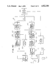
- FIG. 1 is a block diagram showing an embodiment of a foreign substance detecting apparatus according to the present invention.
- FIGS. 2a and 2b are perspective views for explaining how to detect a foreign substance.
- FIGS. 3a to 3e are plan views showing examples of positional relation between picture elements of a photodetector and foreign substances.
- FIGS. 4a and 4b show the shape of foreign substances and the waveform of a detection signal resulting from the foreign substances, respectively.
- FIGS. 5a to 5d are waveform charts showing the outputs of foreign substance detecting circuits.
- FIG. 6 is a graph showing a relation between a pattern angle ⁇ and the output of a detector which receives scattered light from a pattern.
- FIG. 7 is a waveform chart showing the outputs of a detector for various foreign substances.
- FIGS. 8 and 11 are block diagrams showing massive foreign substance judging circuits.
- FIGS. 9 and 10 are graphs for explaining the operations of the judging circuits of FIGS. 8 and 11, respectively.
- FIGS. 12a to 12c are plan views showing the picture element of a detector and the image of a pattern.
- FIG. 13 is a diagram showing an algorithm for determining a pattern angle.
- FIGS. 14, 15a, 15b, 16a and 16b are plan views showing picture elements of a detector and the image of a pattern edge portion.
- FIG. 17 is a plan view showing picture elements of a detector.
- FIG. 18 is a schematic diagram for explaining how foreign substances on a photo-mask are projected onto a wafer.
- FIG. 19a and 19b show the waveform of a detection signal due to transmitted light from a photo-mask and the differentiated one of the detection signal.
- FIGS. 20a to 20f show how a circuit pattern can be detected from a detection signal due to transmitted light.
- FIG. 21 shows how only foreign substances can be extracted from a detection signal due to transmitted light.
- FIG. 22 is a block diagram showing a filmy foreign substance detecting circuit.
- FIG. 23 is a perspective view showing the formation of a defect common to all chips.
- FIG. 24 is a sectional view showing a specimen irradiated obliquely with a light beam.
- FIGS. 25 to 72 are block diagrams showing examples of the fundamental construction of a foreign substance detecting apparatus according to the present invention.
- FIGS. 73 and 84 are block diagrams showing massive foreign substance detecting systems.
- FIG 74 is a perspective view showing a portion of a photo-mask.
- FIG. 75 is a perspective view showing diffracted light from a circuit pattern.
- FIGS. 76 and 78 are plan view showing diffracted light from various circuit patterns.
- FIGS. 77, 79 to 81, 85, 86 and 88 are plan views showing various spatial filters.
- FIGS. 82 and 83 are sectional and plan views showing a photo-mask.
- FIG. 87 is a plan view showing a circuit pattern on a photo-mask.
- FIG. 89 is a sectional view showing a specimen holding stage different from the X-Y-Z stage of FIG. 1.
- FIG. 1 shows the whole construction of the present embodiment.
- the present embodiment is made up of a specimen holding unit 4, an oblique illumination unit 9, a scattered light detection unit 16, a transmitted-light producing illumination unit 21, a transmitted light detection unit 22, and a control unit 35.
- the specimen holding unit 4 includes an X-Y-Z stage 1, a driving system 2 for driving the X-Y-Z stage 1, and holding means 3 for fixing a photomask (or a reticle) 36 which is provided with a pellicle film 37 (for preventing a foreign substance from being deposited on the reticle 36) if necessary, to the stage 1 by the suction method in a state that the photo-mask (or the reticle) 36 is accurately located in relation to and pressed against a positioning pin 3'.
- the oblique illumination unit 9 includes a laser device 5 for emitting a linearly-polarized laser beam, a beam expander 6, a focusing lens 7, and setting means 8 for adjusting the direction and position of the laser beam manually so that the laser beam impinges on the photomask 36 at a predetermined position thereof and has a predetermined incident angle.
- the scattered light detection unit 16 includes an objective lens 10, a half mirror 11, relay lenses 12 and 38, an analyzer 13, an interference filter 14, a spatial filter 26, a one-dimensional solid state pick-up device 15, and a signal amplifier 42.
- the transmitted-light producing illumination unit 21 includes a mercury lamp 17, a ring diaphragm 28, a condenser lens 18, an interference filter 19 and a focusing lens 20.
- the transmitted light detection unit 22 includes the objective lens 10, relay lenses 12 and 39, a phase plate 27, an interference filter 40, and a one-dimensional solid state pick-up device 41.
- the control unit 35 includes a pattern portion extracting circuit (or a specified pattern extracting circuit which will be explained later) 23, a massive foreign substance judging circuit 24, a differentiating circuit 25 for differentiating a detection signal due to transmitted light, a filmy foreign substance judging circuit 30, a stage control system 31, a CRT (cathode ray tube) display 32, a printer 33 and a microcomputer 34.
- the photo-mask 36 is fixed to the X-Y-Z stage 1 by the holding means 3, and the stage 1 can be moved in the Z-direction, to inspect not only the surface of the photo-mask 36 but also the pellicle film 37 provided over the photo-mask.
- the pellicle film 37 is a thin transparent film and prevents a foreign substance from getting near the photo-mask 36.
- the X-stage carries out a periodical motion in the X-direction in such a manner that one-half period includes an accelerating time of about 0.1 sec, a constant velocity time of 0.1 sec and a decelerating time of 0.1 sec, a maximum velocity is about 1 m/sec, and the periodic motion has an amplitude of 200 mm.
- a central portion of the amplitude having a length of 100 mm corresponds to the constant-velocity time
- end portions on both sides of the central portion each having a length of 50 mm correspond to the accelerating or decelerating time.
- the Y-stage moves in a Y-direction by a length of 0.15 mm in synchronism with the beginning of each accelerating time and each decelerating time of the X-stage.
- a time of about 130 seconds is necessary for moving the Y-stage by 100 mm. That is, it takes about 130 seconds to inspect an area of 100 mm ⁇ 100 mm.
- the linearly-polarized beam emitted from the laser device 5 impinges on the photo-mask 36 through the beam expander 6 and the focusing lens 7.
- an incident angle i is set by the setting means 8.
- Scattered light from the photo-mask 36 travels in the scattered light detection unit 16. That is, the scattered light passes through the objective lens 10 and the relay lens 12, and is then reflected from the half mirror 11. The reflected light from the half mirror 11 passes through the interference filter 14 (for intercepting light from the transmitted-light producing illumination unit 21), the spatial filter 26 and the analyzer 13, and is then focused on the one-dimensional solid state pick-up device 15 by the relay lens 38.
- a detection signal from the pick-up device 15 is amplified by the amplifier 42, and then applied to the massive foreign substance judging circuit 24 of the control unit 35.
- the relay lens 12 is set so that light from the center of the exit pupil of the objective lens 10 is focused on the spatial filter 26.
- FIGS. 2a and 2b show how to detect the scattered light from the photo-mask 36 having been subjected to the oblique illumination.
- FIG. 2a shows a case where a single photodetector 29 is used
- FIG. 2b shows a case where a one-dimensional solid state pick-up array 43 is used.
- Each light receiving element of the pick-up array 43 is formed of a silicon photodiode or a GaAsP photodiode.
- the photodiode of the PIN junction type is excellent in response and sensitivity, and hence is suitable for use in the pick-up array of the present embodiment.
- FIGS. 3a to 3b show examples of the positional relation between the light receiving elements (that is, picture elements) of the solid state pick-up array 43 and the images of foreign substances.
- an insensitive region exists between adjacent picture elements of the array 43.
- the array 43 is made up of rectangular picture elements as shown in FIGS. 3a and 3b, when images 44 and 45 of foreign substances are moved on the insensitive regions in a direction perpendicular to one side of a picture element, the image 45 larger than the width of the insensitive region can be detected but the image 44 smaller than the width of the insensitive region cannot be detected as shown in FIG. 3b.
- the array 43 is made up of parallelogrammic picture elements as shown in FIGS.
- FIG. 4a shows a case where a pattern edge 48 and a massive foreign substance 49 each subjected to oblique illumination 47 are scanned with a scattered light detector 50
- FIG. 4b shows the waveform of the output V o of the detector 50.
- peak values V a of the output V o such as shown in FIG. 5a are used.
- the peak value V a can be detected in such a manner that the value of the output V o at a point where the differentiated value V o ' of the output V o changes from positive to negative, is used as the peak value.
- FIG. 5a shows a manner that the value of the output V o at a point where the differentiated value V o ' of the output V o changes from positive to negative
- the output V o is applied to a peak hold circuit which is reset when a predetermined time t has elasped, and the output V b of the peak hold circuit at a reset time is used as the peak value V a .
- the peak value V a may be detected in the following manner. Referring to FIG. 5d, the output V o is applied to a peak hold circuit which is reset when the output V o becomes lower than a predetermined threshold level, and the output V c of the peak hold circuit at a reset time is used as the peak value V a . Referring back to FIGS.
- the S-polarized light from the laser device 5 impinges on the photo-mask 36 at an incident angle i which is set so that a pellicle frame on the photo-mask 36 does not interfere with the S-polarized light as described in JP-A-59-82,727.
- Scattered light from the photo-mask passes through the objective lens 10 and a P-analyzer 13, and is then focused on the detector 29 or 43 by a relay lens (not shown).
- a relay lens not shown.
- FIG. 6 shows a relation between a pattern angle and the detected quantity of light scattered from a pattern edge.
- an angle ⁇ between a direction perpendicular to the traveling direction of the laser beam from the laser device 5 in the oblique illumination unit and a pattern edge 48 is used as the pattern angle.
- the outputs V 2 .0, V 1 .0 and V 0 .5 of a detector for standard foreign substances having diameters of 2 ⁇ m, 1 ⁇ m and 0.5 ⁇ m are also described in the graph of FIG. 6. As can be seen from FIG.
- FIG. 7 shows the output V o of the scattered light detection unit 16 due to the scattered light from each of a large isolated foreign substance 7a, an isolated foreign substance 7b having a diameter of 0.5 ⁇ m, a foreign substance 7c kept in contact with a non-specified pattern and having a diameter of 0.5 ⁇ m, a foreign substance 7d kept in contact with a specified pattern and having a diameter of 0.5 ⁇ m, a non-specified pattern 7e and a specified pattern 7f. Further, two threshold levels V H and V L are set as shown in FIG. 7.
- the output V o of the detection unit When the output V o of the detection unit is not lower than the threshold level V H , the large foreign substance 7a or the foreign substance 7d kept in contact with a specified pattern exists, and thus it is judged that a foreign substance is present.
- the output V o When the output V o is lower than the threshold level V L , it is judged that no foreign substance is present. Further, in a case where the output V o lies in a range from V L to V H and any specified pattern is not detected, it is judged that a foreign substance is present. In a case where the output V o lies in the range from V L to V H and a specified pattern is present, it is judged that no foreign substance is present. That is, when the presence of a specified pattern is expressed by P, the presence D of a foreign substance is given by the following equation:
- FIG. 8 shows an example of a circuit for the above algorithm.
- the output V o of the scattered light detection unit 16 is applied to a comparator 51, to be compared with the threshold level V H , and is also applied to another comparator 52, to be compared with the threshold level V L .
- the output of the comparator 51 is applied to an OR circuit 56 and a NOT circuit 54.
- the output of the transmitted light detection unit 22 is applied to a specified pattern extracting circuit 23, which delivers a signal having a level "1" when a specified pattern is detected.
- the output of the specified pattern extracting circuit 23 is polarity-inverted by a NOT circuit 53, and then applied to an AND circuit 55.
- the AND circuit 55 is also applied with the outputs of the comparator 52 and the NOT circuit 54.
- the output of the AND circuit 55 is applied to the OR circuit 56.
- FIG. 9 shows the output V.sub. ⁇ of the scattered light detection unit for the scattered light from a pattern having a pattern angle of 0° to ⁇ 45°, the output V 0 .5 for the scattered light from a standard foreign substance having a diameter of 0.5 ⁇ m, the output V 0 +V 0 .5 for the scattered light from a 0.5 ⁇ m diameter standard foreign substance which exists in close proximity to a pattern having a pattern angle of 0° to ⁇ 45°, and the threshold levels V H and V L .
- the distance ⁇ V L between the output V 0 .5 and the threshold level V L is a margin for preventing the foreign substance from being missed
- the distance ⁇ V H between the peak value of the output V 74 and the threshold level V H is a margin for preventing the erroneous detection of the pattern.
- the detected quantity of light scattered from a pattern varies with a pattern angle ⁇ .
- a foreign substance is detected by the following algorithm. That is, a pattern angle ⁇ on the photo-mask is first detected by using transmitted light. Then, a threshold level V M is varied as shown in FIG. 10 on the basis of the output V R of the detection unit corresponding to the detected pattern angle and previously stored in a memory.
- the output V o of the scattered light detection unit 16 is not lower than the threshold level V M , it is judged that a foreign substance is present.
- the output V o is lower than the threshold level V M , it is judged that no foreign substance is present.
- FIG. 11 shows an example of a circuit for the present algorithm.
- the output V o of the scattered light detection unit 16 is applied to a comparator 58, to be compared with the threshold level V M .
- the output of the transmitted light detection unit 22 is applied to the pattern portion extracting circuit 23, which detects the pattern angle ⁇ of an inputted pattern.
- the detected pattern angle ⁇ is applied to a V M -level generating circuit 57, and the output V M of the circuit 57 is applied to the comparator 58.
- a specified pattern can be detected by checking whether or not an image of pattern formed by the transmitted light agrees with one of those images of specific patterns which are previously stored in a memory.
- this method it is necessary to extract the image of pattern very accurately, and hence the picture elements of the image pick-up device are required to be small in size. Accordingly, it is necessary to scan a specimen with a light beam a large number of times, and thus a time required for inspecting the specimen becomes long.
- the picture element 63 In a case where a pattern edge 48 is projected onto a rectangular picture element 63 (which may be replaced by a square picture element) of an image pick-up array as shown in FIG. 12a, the picture element 63, as shown in FIG. 12b, delivers an output V o ⁇ A/(A+B) corresponding to the mean position 64 of the pattern edge 48 at the picture element 63 in directions parallel to the longer sides thereof (namely, the position of the pattern edge 48 on that center line of the picture element 63 which is parallel to the longer sides thereof). Accordingly, when a plurality of picture elements are used as shown in FIG. 12c, a pattern angle ⁇ of the edge 48 can be detected from the outputs of the picture elements. As mentioned above, according to this method, a specified pattern can be detected accurately even when large picture elements are used. Accordingly, this method is suitable for the high-speed detection of a foreign substance.
- FIG. 13 shows an example of the detection of a pattern angle according to the above method.
- a block 13a shows an image of a pattern 48 which is formed on the light receiving surface of an image pick-up array by transmitted light, or is formed by scanning a specimen surface with a single photodetector for receiving the transmitted light
- a block 13b shows 3 ⁇ 3 picture elements including a central picture elements 45 for detecting the pattern angle of the pattern 48.
- a block 13c shows respective outputs of the picture elements shown in the block 13b. It is to be noted that the saturation output of a picture element is supposed to be 100 and the actual output of the picture element is normalized on the basis of the saturation output thereof.
- a block 13d shows the sum of the outputs of three picture elements arranged in an X-direction, and the above sum corresponds to the output of the picture element of FIG. 12b.
- a pattern angle ⁇ can be determined from the sum of outputs of three picture elements arranged in one of two adjacent rows and the sum of outputs of three picture elements arranged in the other row.
- a block 13i shows that the pattern angle calculated from the values of the block 13d is used as a pattern angle ⁇ .
- the image of the pattern edge 48 is inclined at a small angle to the long side of the picture element 63 as shown in FIGS. 15a and 15b, the determination of pattern angle by the above calculation is not accurate.
- another pattern angle ⁇ 2 is calculated from the sum of outputs of three picture elements arranged in a Y-direction.
- the pattern angles ⁇ 1 and ⁇ 2 thus obtained are used as follows.
- the angle ⁇ 1 is used as a pattern angle ⁇ .
- the angle ⁇ 2 is used as the pattern angle ⁇ .
- each of two adjacent picture elements has the same output for two arrangements of the image of the pattern 48, as shown in FIGS. 16a and 16b. In order to discriminate the two arrangements from each other, a decision process shown in FIG. 13 is used.
- a pattern has been detected by using transmitted light.
- the pattern may be detected by other illumination methods.
- the laser device 5 is mounted in the oblique illumination unit 9 by the setting means 8.
- the linearly-polarized light 74 emitted from the laser device 5 passes through the beam expander 6 and the focusing lens 7, and then impinges on the photo-mask 36 at an incident angle i.
- Light reflected and diffracted from the photo-mask 36 passes through the objective lens 10 and the relay lens 12, and is then focused on the spatial filter 26. That is, the real image of the light source of the linearly-polarized light is formed on the spatial filter 26 by the beam expander 6, the focusing lens 7, the objective lens 10 and the relay lens 12.
- the Fraunhofer diffraction image of the pattern 48 provided on the photo-mask 36 is formed in a plane which contains the spatial filter 26.
- the plane of polarization of the linearly-polarized light 74 is made perpendicular to the plane of incidence defined by the linealy-polarized light 74 and an optical axis 75, to obtain P-polarized light, or is made parallel to the plane of incidence to obtain S-polarized light.
- the above optical arrangement may be modified as follows. That is, the diameter dp of the light beam incident upon the focusing lens 7 is put in a range from 0.5 to 2 mm and the distance Lp between the focusing lens 7 and the photo-mask 36 is put in a range from 30 to 100 mm, to form the image of the light source of the above light beam on the photo-mask 36. Further, the spatial filter 26 is disposed in a Fourier transform plane which is formed only by the objective lens 10 and the relay lens 12. According to this optical arrangement, light rays incident upon the photo-mask 36 are substantially parallel to each other, and hence it can be considered that the light rays are Fourier-transformed only by the objective lens 10 and the relay lens 12. In this case, an illuminated portion on the photo-mask 36 has the form of an ellipse, and the length a i of the minor axis of the ellipse is given by the following equation:
- the length a i is determined in accordance with a light intensity necessary for the detection of a foreign substance and an area to be illuminated.
- the beam diameter dp is made equal to 1 mm and the distance Lp is made equal to 50 mm, to make the length a i equal to 40 ⁇ m.
- the images of the pattern 48 and the foreign substance 49 which exist on the photo-mask 36 are formed on the one-dimensional pick-up device 15 by the objective lens 10 and the relay lenses 12 and 38.
- the spatial filter 26 is placed in an image formation plane, on which the image of the light source of the beam 74 is formed by the beam expander 6, the focusing lens 7, the relay lens 12 and the objective lens 10.
- the analyzer 13 (that is, a polarization filter) is disposed at substantially the same position as the spatial filter 26.
- the plane of polarization of the analyzer 13 is directed so that the analyzer 13 intercepts the light beam 74. That is, for the S-polarized light beam, the plane of polarization of the analyzer 13 is made perpendicular to the above-mentioned plane of incidence. For the P-polarized light beam, the plane of polarization of the analyzer 13 is made parallel to the plane of incidence.
- the analyzer 13 may be disposed at a desired position between the photo-mask 36 and the one-dimensional solid state pick-up device 15.
- the spatial filter 26 may be disposed at a position which exists between the photo-mask 36 and the objective lens 10 and is close to the objective lens 10. The reason for this is as follows.
- the light beam 74 is substantially formed of parallel light rays and the pattern 48 on the photo-mask 36 is very fine. Accordingly, the Fraunhofer diffraction image of the pattern can be formed without using the objective lens 10 and others. In a case where a filmy foreign substance is to be detected, however, it is desirable that an optical system for detecting the filmy foreign substance does not contain the spatial filter 26.
- a collective lens including the relay lens 12 is used as the objective lens 10 and the image of the light source of the beam 74 is formed within the objective lens 10 by the beam expander 6, the focusing lens 7 and the objective lens 10, it is required to dispose the spatial filter 26 at the image formation position existing behind the relay lens 12.
- a Fourier transform lens may be used as the relay lens 12. In this case, the Fourier transform image of the pattern 48 becomes sharp, and thus the light from the pattern 48 can be intercepted effectively by the spatial filter.
- the interference filter 14 is used for intercepting light from the transmitted-light generating illumination unit 26, and thus can extract only the light from the laser device 5.
- the shape of the spatial filter 26 is to be appropriately determined in accordance with the method of illumination and the state of polarization of light incident on the spatial filter.
- FIG. 74 is an enlarged view of a photo-mask 105.
- a pattern 107 having an edge 147 parallel to a direction 148 is formed on a substrate 146.
- the pattern 107 and the substrate 146 are made of chromium oxide and SiO 2 , respectively.
- FIG. 75 is a sketch showing a positional relation among light 155 incident on the photo-mask 105, diffracted light rays 159 and 160 from the pattern 107 parallel to the direction 148, and the aperture 164 of the objective lens 10.
- reference numerals 158, 162 and 163 designate the planes of polarization.
- the planes of polarization 162 and 163 of the diffracted light rays 159 and 160 are the planes of polarization at the intersections 161 and 198 of the spherical surface 165 and the diffracted light rays 159 and 160. Further, a circle 166 on the spherical surface 165 passes through the intersections 161 and 198.
- FIG. 76 is a plan view of the sketch of FIG. 75.
- that circle on the spherical surface 165 which passes through the intersections of the spherical surface 165 and the diffracted rays corresponding to one of four pattern directions, is indicated by one of four straight lines 199 to 202.
- the intersection of the incident light 155 and the spherical surface 165 and the intersection of the outgoing light 156 and the spherical surface 165 are indicated by points 205 and 157, respectively.
- E S and E P indicate the intensities of S- and P-polarized components of the incident light
- R S and R P indicate the intensities of S- and P-polarized components of the reflected light
- S(i) and P(i) are given by the following equations: ##EQU2##
- the plane of polarization 162 of the diffracted light ray 159 at the intersection 161 can be calculated from the equations (2) and (3).
- the edge 147 of the pattern 107 is formed of three planes 149, 150 and 152 having normal vectors 152, 153 and 154, and the reflection from each of the above planes is calculated.
- the direction and the plane of polarization of the reflected light from each of the planes 149 to 151 for a case where the P-polarized light impinges on the planes 149 to 151 are calculated by the equation (2), to be used as the direction and the plane of polarization 162 of the diffracted light ray 159.
- the planes of polarization 162 thus obtained are indicated by arrows 162 in FIG. 76.
- the diffracted light from the pattern can be intercepted effectively by setting the incident angle i of the incident light 155 appropriately and by using the spatial filter 26 and the analyzer 13.
- diffracted light within an angular range 167 does not pass through the aperture 164 of the objective lens 10. That is, when the incident angle i of the incident light is set so that the diffracted light from the pattern lies in the angular range 167, the diffracted light is intercepted. When the incident angle i is made large, the outgoing point 157 moves to a point 174 which is farther away from the aperture 164 than the point 157, and thus the diffracted light within an angular range 206 wider than the angular range 167 is intercepted.
- the diffracted light from the pattern parallel to a direction within an angular range 171 of FIG. 76 such as the pattern parallel to the direction 148 perpendicular to the circle 166 can be intercepted.
- the plane of polarization of the polarized light within an angular range 168 is substantially parallel to the plane of incidence. Meanwhile, the plane of polarization of the polarized light within angular ranges 169 and 170 is not parallel to the plane of incidence. Hence, the diffracted light within the angular range 168 is intercepted by the polarization filter (namely, analyzer) 13, and the diffracted light within angular ranges 169 and 170 is intercepted by the spatial filter 26.
- the polarization filter namely, analyzer
- FIG. 77 shows the shape of the spatial filter 26.
- the spatial filter 26 includes a light intercepting portion 175 and a light transmitting portion 176.
- An edge 208 pf the spatial filter 26 has the form of a curved line for the reason that the aperture 164 is in a plane, and the locus of the intersection of the diffracted light 159 and the aperture 164 forms a curved line.
- the aperture 164 lies in the Fourier transform plane, and hence the shape of the spatial filter 26 is determined on the basis of the intensity distribution of the diffracted light at the aperture 164. That is, the shape of the spatial filter 26 is made similar to the cross-sectional shape of the diffracted light beam at the aperture 164. At this time, it is to be noted that the aperture 164 is formed of a plane.
- the diffracted light in the angular range 168 is caused by the pattern parallel to a direction within an angular range 172, and the diffracted light in the angular ranges 169 and 170 is caused by the pattern parallel to a direction within angular ranges 173 and 174.
- the diffracted light from each of patterns having various directions can be intercepted by setting the incident angle i appropriately, setting the plane of polarization of the polarization filter (namely, analyzer) 13 appropriately and selecting the shape of the spatial filter 26 appropriately.
- the planes of polarization of scattered light rays from a foreign substance are not parallel, though the planes of polarization of diffracted light rays from a pattern are parallel to each other. Accordingly, the scattered light within the angular range 168 may have the plane of polarization which is not parallel to the plane of polarization 172, and hence can not pass through the filters 13 and 26.
- the plane of polarization of scattered light from a foreign substance is discussed on pages 652 to 656 of a publication entitled "Principle of Optics" by Born and Wolf.
- FIG. 78 shows the plane of polarization of diffracted light from the pattern for a case where S-polarized light (namely, linearly-polarized light having the electric field vector perpendicular to the plane of incidence) impinges on the photo-mask.
- S-polarized light namely, linearly-polarized light having the electric field vector perpendicular to the plane of incidence
- the diffracted light within angular ranges 178 and 210 is intercepted by the same spatial filter as shown in FIG. 77, and the diffracted light within an angular range 177 is intercepted by rotating the plane of polarization of the analyzer 13 for the diffracted light within the angular range 168 of FIG. 76, by an angle of 90°.
- FIG. 79 shows the plane of polarization 211 of linearly-polarized light incident upon the photo-mask vertically and the plane of polarization 212 of the diffracted light from a pattern.
- the diffracted light within angular ranges 179, 180, 181 and 182 can be intercepted by the spatial filter 26 having such a shape as shown in FIG. 80, and the diffracted light within ranges 183, 184, 185 and 186 can be intercepted by the analyzer 13.
- the photo-mask 105 is provided with a pellicle structure for preventing a foreign substance from being attached to the photo-mask.
- the pellicle structure is made up of a thin transparent film (namely, pellicle film) 136 and a pellicle frame 137 for holding the pellicle film 136.
- a wide area 139 on the photo-mask is not illuminated with incident light, since the incident light is intercepted by the pellicle frame 137. This problem can be solved by using two oblique illumination units 9 and 220.
- the oblique illumination units 9 and 220 equal in construction are disposed so that, as shown in FIG. 83, the incident light 138 from the unit 9 and the incident light 141 from the unit 220 are substantially symmetrical with respect to the optical axis of the present embodiment.
- the reflected light from the photo-mask is divided by a half mirror 188, and moreover a spatial filter 189, an analyzer (namely, polarization filter) 190, an interference filter 191, a relay lens 110 and a one-dimensional solid state pick-up device 192 are added to the scattered light detection unit 16 of FIG. 73.
- the 81 and the turned-up version thereof are used as the spatial filters 26 and 189 of FIG. 84, respectively.
- the incident light 141 is used, and the reflected light from the photo-mask is detected by the pick-up device 192.
- the pick-up device 192 is used to inspect the area 139 of FIG. 83.
- the area 139 of FIG. 83 may be inspected by rotating the photo-mask round the optical axis by an angle of 180°, without using the oblique illumination unit 220.
- the light 138 from the oblique illumination 9 is made different in wavelength from the light 141 from the oblique illumination unit 220. That is, the light 138 has a wavelength ⁇ 1 and the light 141 has a wavelength ⁇ 2 .
- the wavelengths ⁇ 1 and ⁇ 2 can be separated from each other by using a wavelength separation mirror in place of the half mirror 188, and moreover the light sources in the oblique illumination units 16 and 220 are not required to be alternately turned off.
- the use of two oblique illumination units produces another effect. That is, as shown in FIG. 74, an actual, fine foreign substance is not symmetrical with respect to the center axis thereof. Accordingly, the reflecting surface of the foreign substance for the incident light 138 is different in size and shape from the reflecting surface for the incident light 141, and hence the scattered light from the former reflecting surface is different in intensity and plane of polarization from the scattered light from the latter reflecting surface.
- the incident light 138 and the incident light 141 there is a fear that the foreign substance is missed.
- both of the light 138 and the light 141 are used, there is a fair chance for the foreign substance on an area 320 (shown in FIG. 83) to be detected by the light 138 or 141, and thus the reliability of the detection of foreign substance is enhanced.
- a foreign substance can be detected without requiring the members 110, 188, 189, 190, 191 and 192 in the scattered light detection unit 16.
- the reflected light from the pattern 107 can be intercepted.
- a shading plate together with the analyzer of FIG. 86.
- the pattern 107 on an actual photo-mask 105 is often formed of pattern portions having a pattern angle equal to 0° and pattern portions having a pattern angle of 90°.
- a spatial filter shown in FIG. 88 since the scattered light from the pattern portions having a pattern angle equal to 0° can be intercepted by a light intercepting portion 175.
- the scattered light from the pattern portions does not impinge on the objective lens 10.
- the plane of polarization of incident light, the incident angle i, the shape of the spatial filter, and the plane of polarization of the analyzer are to be determined on the basis of the above facts.
- the transmitted-light producing illumination unit 21 of FIG. 1 operates as follows. Light emitted from a light source 17 (for example, a mercury lamp or a mercury-xenon lamp) passes through the wavelength selection filter 19, the condenser lens 18, the ring diaphragm 28 and the focusing lens 20, and then impinges upon the photo-mask.
- the ring diaphragm 28 is used only when a phase contrast microscope is formed as mentioned later.
- the transmitted light having passed through the photo-mask 36 is converted into convergent light by the objective lens 10, and then passes through the relay lens 12, the half mirror 11, the interference filter 40 for separating the transmitted light from the scattered light, the phase plate 27 and the relay lens 39.
- the light from the lens 39 is focused on the one-dimensional solid state pick-up device 41.
- the phase plate 27 is used only when the phase contrast microscope is formed.
- a detection signal indicative of an image of the photo-mask 36 formed by the transmitted light is sent to the differentiating/emphasizing circuit 25, to emphasize the filmy foreign substance, and the filmy foreign substance is discriminated from the pattern by the filmy foreign substance judging circuit 30, to be detected.
- the filter 19 for selecting the same wavelength as that of the exposing light is included in the illumination unit 21. It is needless to say that the filter 19 may be disposed at a desired position between the light source 17 and the photo-mask 36.
- the defferentiating/emphasizing circuit 25 for the detection signal due to transmitted light will be explained below.
- the light intensity I on the wafer 59 is greatly reduced at a position corresponding to the foreign substance 60. That is, the highly opaque foreign substance 60 has a great influence on the projection of the photo-mask 36 on the wafer 59.
- the light intensity I on the wafer 59 is reduced only a little at a position corresponding to the foreign substance 61. That is, the influence of the slightly opaque foreign substance 61 on the above projection is less than that of the highly opaque foreign substance on the projection.
- the transmitted light detection unit 22 is formed of a phase contrast microscope, or a detection signal V T due to transmitted light is electrically differentiated. As shown in FIG. 19, a signal
- FIG. 20a shows the photo-mask 36 having a pattern 48, a large, filmy, slightly-opaque foreign substance 66 and a small, filmy, highly-opaque foreign substance 67.
- the pattern 48 is formed of a highly-opaque metal film, and hence the light passing through the photo-mask 36 is weakened at the pattern 48.
- FIGS. 20b to 20d show detection signals V T due to the transmitted light from the photo-mask of FIG. 20a. When the detection signal V T has such a waveform as shown in FIG.
- FIG. 20c shows a detection signal V T which has been obtained by using an optical system which is lower in resolving power than an optical system for obtaining the detection signal of FIG. 20b.
- FIG. 20d shows a detection signal V T which has been obtained by using a detector which is larger in size than a detector for obtaining the detection signal of FIG. 20b.
- detection systems for obtaining the detection signals of FIGS. 20c and 20d are both low in resolving power. In the detection signals of FIGS.
- a reduction in signal level due to the highly-opaque foreign substance 67 is less than a reduction in signal level due to the pattern 48, and hence the foreign substances 66 and 67 can be discriminated from the pattern 48 by using an appropriate threshold level V n or V g .
- a detection system having an appropriate resolving power and an appropriate threshold level
- a binary signal V p shown in FIG. 2e can be extracted from a detection signal.
- a signal V M shown in FIG. 20f is obtained. Referring now to FIG. 21, when the differentiated signal
- FIG. 22 shows the circuit configuration of the filmy foreign substance detecting circuit 30.
- a detection signal V T from a transmitted-light detecting circuit 71 is differentiated by the differentiating/emphasizing circuit 25, to obtain a differentiated signal
- the detection signal V T is also compared with a threshold level V n or V g by a comparator circuit 77, to obtain a binary signal V p , which is applied to a picture-element enlarged circuit 78 to obtain a masking signal V M .
- the masking signal V M is applied to one input terminal of an AND circuit 80 through an inverter 53, and the other input terminal of the AND circuit 80 is applied with the differentiated signal
- an output signal V S from the AND circuit 80 is the logical sum of the outputs of the differentiating circuit 25 and the inverter 59, and is not affected by the pattern.
- the signal V S is compared with a threshold level V k by a comparator circuit 79, to obtain a foreign substance detection signal D.
- the transmitted-light producing illumination unit 21 of FIG. 1 In the transmitted-light producing illumination unit 21 of FIG. 1, light from the light source 17 impinges on the ring diaphragm 28 having a ring-shaped aperture through the condenser lens 18 and the interference filter 19, and the light from the ring diaphragm 28 impinges on the back side of the photo-mask 36 through the focusing lens 20.
- the transmitted light from the photo-mask 36 passes through the objective lens 10, the relay lens 12, the half mirror 11 and the interference filter 40 for intercepting light from the oblique illumination unit 9, and is then focused on the phase plate 27.
- phase contrast microscope is explained in many publications, for example, a Japanese publication entitled “OYO-KOGAKU (Applied optics)" by H. Kubota, pages 129 to 136, and hence explanation thereof will be omitted.
- a filmy foreign substance to be detected by the phase contrast microscope is required to produce a detectable phase difference, that is, is required to a thickness of 10 nm or more.
- a thick filmy foreign substance can be detected, since variations in thickness thereof cause a phase difference.
- a filmy foreign substance having a thickness of 10 nm to 10 ⁇ m can be detected by the phase contrast microscope.
- phase contrast microscope When the phase contrast microscope is used for detecting a filmy foreign substance, only that portion of the field of view where a phase difference is generated, that is, only the portion corresponding to the foreign substance can be made bright. Accordingly, it is not required to detect the pattern in the above-mentioned manner, and thus the system for detecting the filmy foreign substance can be simplified in structure.
- FIG. 23 shows that a foreign substance 49 on a photo-mask 71 is repeatedly projected onto a wafer 59
- FIG. 24 shows that light from the oblique illumination unit is scarcely scattered from a filmy foreign substance 73.
- FIGS. 25 to 72 show examples of the circuit configuration of a foreign substance detecting apparatus according to the present invention.
- like reference numerals designate like circuits or parts.
- a specimen (for example, photo-mask) 36 is irradiated with the light from the oblique illumination unit 9 and the light from the transmitted-light producing illumination unit 21.
- An image of the photo-mask 36 formed by transmitted light is converted by the transmitted light detection unit 22 into a detection signal.
- a filmy foreign substance detecting circuit 83 performs a differentiating/emphasizing operation for the detection signal due to transmitted light, if necessary, to detect a filmy foreign substance.
- An image of the photo-mask formed by scattered light is converted by the scattered light detection unit 16 into another detection signal.
- a massive foreign substance detecting circuit 93 detects a massive foreign substance from the detection signal due to scattered light. The filmy and massive foreign substances thus detected are displayed by a foreign substance display device 82 after the double detection of each foreign substance has been prevented by an OR circuit 81.
- the circuit configuration of FIG. 26 is different from the circuit configuration of FIG. 25 in that the filmy foreign substance detected by the foreign substance detecting circuit 83 is displayed by a filmy foreign substance display device 84 before sent to the OR circuit 81, and the massive foreign substance detected by the massive foreign substance detecting circuit 93 is displayed by a massive foreign substance display device 85 before sent to the OR circuit 81.
- the circuit configuration of FIG. 27 is different from the circuit configuration of FIG. 25 in that the pattern extracting circuit 23 is additionally provided.
- false information on a pattern portion is removed from the result of judgement of a filmy foreign substance judging circuit 86 (which includes the differentiating/emphasizing circuit 25, if necessary) by a pattern portion inhibiting circuit 87 which pattern is for detecting the transmitted light, and false information on the pattern portion due to scattered light is removed from the result of judgment of a massive foreign substance judging circuit 88 by another pattern portion inhibiting circuit 89 which pattern portion is for detecting the scattered light.
- the circuit configuration of FIG. 28 is different from the circuit configuration of FIG. 26 in that the pattern extracting circuit 23 and the pattern portion inhibiting circuits 87 and 89 are provided.
- the circuit configuration of FIG. 29 is different from the circuit configuration of FIG. 27 in that the pattern portion inhibiting circuits 87 and 89 are provided before the foreign substance judging circuits 86 and 88, respectively.
- the circuit configuration of FIG. 30 is different from the circuit configuration of FIG. 28 in that the pattern portion inhibiting circuits 87 and 89 are provided before the foreign substance judging circuits 86 and 88, respectively.
- an analyzer or the combination of a spatial filter and an analyzer may be used for optically inhibiting the image of a pattern portion.
- FIGS. 31 and 32 are different from the circuit configurations of FIGS. 25 and 26, respectively, in that an optical element (that is, a spatial filter, an analyzer, or the combination of a spatial filter and an analyzer) 96 for detecting scattered light, a light source 94 for phase contrast microscope and a phase plate 95 for phase contrast microscope are used to optically inhibit the image of a pattern portion.
- an optical element that is, a spatial filter, an analyzer, or the combination of a spatial filter and an analyzer
- the circuit configurations of FIGS. 33 to 36 are different from the circuit configurations of FIGS. 27 to 30 in that the optical element (that is, the spatial filter, the analyzer, or the combination of the spatial filter and the analyzer) 96 and the phase plate 95 are used together with the pattern extracting circuit 23 and the pattern portion inhibiting circuits 87 and 89, to inhibit a pattern portion optically and electrically.
- the optical element that is, the spatial filter, the analyzer, or the combination of the spatial filter and the analyzer
- FIGS. 37, 38, 40, 41, 43, 44, 46, 47, 49, 50, 52 and 53 are different from the circuit configurations of FIGS. 25 to 36 in that a movable stage (namely, X-Y-Z stage) 1 for causing the specimen 36 to perform a scanning operation and a driving system 2 for driving the stage 1 are provided.
- a movable stage namely, X-Y-Z stage
- driving system 2 for driving the stage 1
- the curcuit configurations of FIGS. 39, 42, 45, 48, 51 and 54 are different from the circuit configurations of FIGS. 38, 41, 44, 47, 50 and 53, respectively, in that the result of detection of a filmy foreign substance and the position coordinates of the detected filmy foreign substance are displayed by the filmy foreign substance display device 84, and the result of detection of a massive foreign substance and the position coordinates of the detected massive foreign substance are displayed by the massive foreign substance display device 85.
- FIGS. 55 to 72 are different from the circuit configurations of FIGS. 37 to 54 in that the movable stage 1 and the driving system 2 are not provided, but a movable detection system 90, holding mechanism 91 for causing the detection system 90 to perform a scanning operation and a driving system 92 for driving the holding mechanism 91 are provided.
- the X-Y-Z stage 1 of FIG. 1 may be replaced by an X- ⁇ -Z stage shown in FIG. 89.
- the X- ⁇ -Z stage is made up of an X-stage 333, an X-stage driving system 2, a ⁇ -stage (namely, rotatable stage) 335, a ⁇ -stage gear 332, a ⁇ -stage driving system 331, a mask 336, clamp means 3 for fixing a specimen 36, and a Z-stage (not shown) capable of moving in a Z-direction to place a focal point on the photo-mask 36.
- the ⁇ -stage can rotate at a constant speed of four revolutions per sec, and the X-stage 333 can move at a constant speed of 0.6 mm/sec in a distance of about 70 mm. Accordingly, it takes about 120 seconds to scan an area of 100 mm ⁇ 100 mm with a light beam. Further, the light incident upon the remaining area on the specimen surface other than an area to be inspected, is intercepted by the mask 336 coupled with the ⁇ -stage 335.
- a foreign substance detecting apparatus for detecting a foreign substance on a reticle or photo-mask having a desired circuit pattern and used for forming a large scale integration circuit, in which apparatus the reflected light from the circuit pattern is eliminated, and thus only a fine massive foreign substance and a filmy foreign substance can be detected without being disturbed by the circuit pattern.
- the circuit pattern on the photo-mask is detected by transmitted light from the photo-mask, and thus the scattered light from a foreign substance can be discriminated from the scattered light from the circuit pattern. Accordingly, it is possible to detect a foreign substance of the order of submicrons which cannot be detected by the prior art.
- an edge portion of a filmy foreign substance can be emphasized by differentiating a detection signal due to transmitted light.
- a detection signal due to transmitted light.
Abstract
Description
D=(V.sub.o ≧V.sub.H)∪{(V.sub.o <V.sub.H)∩(V.sub.o ≧V.sub.L)∩P}
a.sub.i =1.22·λ·Lp/dp . . . (1)
(R.sub.S, R.sub.P)=(S(i)E.sub.S, P(i)E.sub.P) . . . (2)
Claims (12)
Applications Claiming Priority (8)
| Application Number | Priority Date | Filing Date | Title |
|---|---|---|---|
| JP14951986A JPH0752156B2 (en) | 1986-06-27 | 1986-06-27 | Foreign matter inspection device |
| JP14951786A JPH0646182B2 (en) | 1986-06-27 | 1986-06-27 | Apparatus and method for inspecting foreign matter on mask |
| JP61149520A JPS636854A (en) | 1986-06-27 | 1986-06-27 | Foreign substance inspection apparatus |
| JP61-149517 | 1986-06-27 | ||
| JP61-149516 | 1986-06-27 | ||
| JP61-149519 | 1986-06-27 | ||
| JP61-149520 | 1986-06-27 | ||
| JP61149516A JPS636442A (en) | 1986-06-27 | 1986-06-27 | Method and device for foreign matter inspection |
Publications (1)
| Publication Number | Publication Date |
|---|---|
| US4922308A true US4922308A (en) | 1990-05-01 |
Family
ID=27472938
Family Applications (1)
| Application Number | Title | Priority Date | Filing Date |
|---|---|---|---|
| US07/067,136 Expired - Lifetime US4922308A (en) | 1986-06-27 | 1987-06-29 | Method of and apparatus for detecting foreign substance |
Country Status (1)
| Country | Link |
|---|---|
| US (1) | US4922308A (en) |
Cited By (27)
| Publication number | Priority date | Publication date | Assignee | Title |
|---|---|---|---|---|
| US5185516A (en) * | 1989-12-29 | 1993-02-09 | Nippon Steel Corporation | Card-type IC-mounting board |
| US5197105A (en) * | 1990-05-30 | 1993-03-23 | Dainippon Screen Mfg. Co. Ltd. | Method of reading optical image of inspected surface and image reading system employabale therein |
| US5214712A (en) * | 1990-09-11 | 1993-05-25 | Matsushita Electric Industrial Co., Ltd. | Pattern inspection system for inspecting defect of land pattern for through-hole on printed board |
| US5301248A (en) * | 1987-11-09 | 1994-04-05 | Hitachi, Ltd. | Method for pattern inspection and apparatus therefor |
| US5300972A (en) * | 1992-02-10 | 1994-04-05 | Mitsubishi Denki Kabushiki Kaisha | Projection exposure apparatus |
| US5331396A (en) * | 1991-10-08 | 1994-07-19 | Matsushita Electric Industrial Co., Ltd. | Foreign matter detection device |
| US5365330A (en) * | 1991-11-27 | 1994-11-15 | Nikon Corporation | Foreign particle inspection apparatus |
| US5377278A (en) * | 1992-03-26 | 1994-12-27 | Sumitomo Wiring Systems, Ltd. | Method and apparatus for inspecting a solderless terminal by image processing |
| US5410400A (en) * | 1991-06-26 | 1995-04-25 | Hitachi, Ltd. | Foreign particle inspection apparatus |
| US5459794A (en) * | 1993-07-15 | 1995-10-17 | Ninomiya; Takanori | Method and apparatus for measuring the size of a circuit or wiring pattern formed on a hybrid integrated circuit chip and a wiring board respectively |
| US5539514A (en) * | 1991-06-26 | 1996-07-23 | Hitachi, Ltd. | Foreign particle inspection apparatus and method with front and back illumination |
| US6045976A (en) * | 1992-06-02 | 2000-04-04 | Fujitsu, Limited | Optical exposure method |
| US6118525A (en) * | 1995-03-06 | 2000-09-12 | Ade Optical Systems Corporation | Wafer inspection system for distinguishing pits and particles |
| US20010019625A1 (en) * | 1999-10-13 | 2001-09-06 | Boaz Kenan | Method and apparatus for reticle inspection using aerial imaging |
| US6396579B1 (en) * | 1997-03-10 | 2002-05-28 | Shin-Etsu Chemical Co., Ltd. | Method, apparatus, and system for inspecting transparent objects |
| US6486964B2 (en) * | 1998-11-30 | 2002-11-26 | Olympus Optical Co., Ltd. | Measuring apparatus |
| US20020180985A1 (en) * | 2000-09-20 | 2002-12-05 | Dan Wack | Methods and systems for determining at least one characteristic of defects on at least two sides of a specimen |
| EP1353165A2 (en) * | 1994-07-13 | 2003-10-15 | KLA-Tencor Corporation | Automated photomask inspection apparatus and method |
| US20050206887A1 (en) * | 1991-04-02 | 2005-09-22 | Hiroshi Morioka | Method and apparatus for analyzing the state of generation of foreign particles in semiconductor fabrication process |
| US7072502B2 (en) | 2001-06-07 | 2006-07-04 | Applied Materials, Inc. | Alternating phase-shift mask inspection method and apparatus |
| US20070146697A1 (en) * | 1991-04-02 | 2007-06-28 | Minori Noguchi | Apparatus and method for testing defects |
| US20070229813A1 (en) * | 2006-03-31 | 2007-10-04 | Kabushiki Kaisha Topcon | Surface inspection method and surface inspection device |
| US7349090B2 (en) | 2000-09-20 | 2008-03-25 | Kla-Tencor Technologies Corp. | Methods and systems for determining a property of a specimen prior to, during, or subsequent to lithography |
| US7751046B2 (en) | 2000-09-20 | 2010-07-06 | Kla-Tencor Technologies Corp. | Methods and systems for determining a critical dimension and overlay of a specimen |
| US20110194101A1 (en) * | 2008-10-15 | 2011-08-11 | Tachizaki Takehiro | Supersensitization of defect inspection method |
| US20120274931A1 (en) * | 2009-11-18 | 2012-11-01 | Yuko Otani | Defect detection method and defect detection device and defect observation device provided with same |
| US20130271754A1 (en) * | 2010-12-27 | 2013-10-17 | Hitachi High-Technologies Corporation | Inspection apparatus |
Citations (5)
| Publication number | Priority date | Publication date | Assignee | Title |
|---|---|---|---|---|
| US3972616A (en) * | 1974-09-09 | 1976-08-03 | Tokyo Shibaura Electric Co., Ltd. | Apparatus for detecting the defects of the mask pattern using spatial filtering |
| US4419013A (en) * | 1981-03-30 | 1983-12-06 | Tre Semiconductor Equipment Corporation | Phase contrast alignment system for a semiconductor manufacturing apparatus |
| US4595289A (en) * | 1984-01-25 | 1986-06-17 | At&T Bell Laboratories | Inspection system utilizing dark-field illumination |
| US4610541A (en) * | 1983-04-07 | 1986-09-09 | Nippon Kogaku K. K. | Foreign substance inspecting apparatus |
| US4669885A (en) * | 1982-03-23 | 1987-06-02 | Canon Kabushiki Kaisha | Apparatus for inspecting negatives |
-
1987
- 1987-06-29 US US07/067,136 patent/US4922308A/en not_active Expired - Lifetime
Patent Citations (5)
| Publication number | Priority date | Publication date | Assignee | Title |
|---|---|---|---|---|
| US3972616A (en) * | 1974-09-09 | 1976-08-03 | Tokyo Shibaura Electric Co., Ltd. | Apparatus for detecting the defects of the mask pattern using spatial filtering |
| US4419013A (en) * | 1981-03-30 | 1983-12-06 | Tre Semiconductor Equipment Corporation | Phase contrast alignment system for a semiconductor manufacturing apparatus |
| US4669885A (en) * | 1982-03-23 | 1987-06-02 | Canon Kabushiki Kaisha | Apparatus for inspecting negatives |
| US4610541A (en) * | 1983-04-07 | 1986-09-09 | Nippon Kogaku K. K. | Foreign substance inspecting apparatus |
| US4595289A (en) * | 1984-01-25 | 1986-06-17 | At&T Bell Laboratories | Inspection system utilizing dark-field illumination |
Cited By (44)
| Publication number | Priority date | Publication date | Assignee | Title |
|---|---|---|---|---|
| US5301248A (en) * | 1987-11-09 | 1994-04-05 | Hitachi, Ltd. | Method for pattern inspection and apparatus therefor |
| US5185516A (en) * | 1989-12-29 | 1993-02-09 | Nippon Steel Corporation | Card-type IC-mounting board |
| US5197105A (en) * | 1990-05-30 | 1993-03-23 | Dainippon Screen Mfg. Co. Ltd. | Method of reading optical image of inspected surface and image reading system employabale therein |
| US5214712A (en) * | 1990-09-11 | 1993-05-25 | Matsushita Electric Industrial Co., Ltd. | Pattern inspection system for inspecting defect of land pattern for through-hole on printed board |
| US7443496B2 (en) * | 1991-04-02 | 2008-10-28 | Hitachi, Ltd. | Apparatus and method for testing defects |
| US20070146697A1 (en) * | 1991-04-02 | 2007-06-28 | Minori Noguchi | Apparatus and method for testing defects |
| US7177020B2 (en) * | 1991-04-02 | 2007-02-13 | Renesas Technology Corp. | Method and apparatus for analyzing the state of generation of foreign particles in semiconductor fabrication process |
| US20050206887A1 (en) * | 1991-04-02 | 2005-09-22 | Hiroshi Morioka | Method and apparatus for analyzing the state of generation of foreign particles in semiconductor fabrication process |
| US5410400A (en) * | 1991-06-26 | 1995-04-25 | Hitachi, Ltd. | Foreign particle inspection apparatus |
| US5539514A (en) * | 1991-06-26 | 1996-07-23 | Hitachi, Ltd. | Foreign particle inspection apparatus and method with front and back illumination |
| US5331396A (en) * | 1991-10-08 | 1994-07-19 | Matsushita Electric Industrial Co., Ltd. | Foreign matter detection device |
| US5365330A (en) * | 1991-11-27 | 1994-11-15 | Nikon Corporation | Foreign particle inspection apparatus |
| US5300972A (en) * | 1992-02-10 | 1994-04-05 | Mitsubishi Denki Kabushiki Kaisha | Projection exposure apparatus |
| US5377278A (en) * | 1992-03-26 | 1994-12-27 | Sumitomo Wiring Systems, Ltd. | Method and apparatus for inspecting a solderless terminal by image processing |
| US6045976A (en) * | 1992-06-02 | 2000-04-04 | Fujitsu, Limited | Optical exposure method |
| US6420094B1 (en) | 1992-06-02 | 2002-07-16 | Fujitsu Limited | Optical exposure method |
| US5459794A (en) * | 1993-07-15 | 1995-10-17 | Ninomiya; Takanori | Method and apparatus for measuring the size of a circuit or wiring pattern formed on a hybrid integrated circuit chip and a wiring board respectively |
| EP1353165A3 (en) * | 1994-07-13 | 2004-01-28 | KLA-Tencor Corporation | Automated photomask inspection apparatus and method |
| EP1353165A2 (en) * | 1994-07-13 | 2003-10-15 | KLA-Tencor Corporation | Automated photomask inspection apparatus and method |
| US6509965B2 (en) | 1995-03-06 | 2003-01-21 | Ade Optical Systems Corporation | Wafer inspection system for distinguishing pits and particles |
| US6118525A (en) * | 1995-03-06 | 2000-09-12 | Ade Optical Systems Corporation | Wafer inspection system for distinguishing pits and particles |
| US6292259B1 (en) | 1995-03-06 | 2001-09-18 | Ade Optical Systems Corporation | Wafer inspection system for distinguishing pits and particles |
| US6396579B1 (en) * | 1997-03-10 | 2002-05-28 | Shin-Etsu Chemical Co., Ltd. | Method, apparatus, and system for inspecting transparent objects |
| US6486964B2 (en) * | 1998-11-30 | 2002-11-26 | Olympus Optical Co., Ltd. | Measuring apparatus |
| US20010019625A1 (en) * | 1999-10-13 | 2001-09-06 | Boaz Kenan | Method and apparatus for reticle inspection using aerial imaging |
| US7133548B2 (en) | 1999-10-13 | 2006-11-07 | Applied Materials, Inc. | Method and apparatus for reticle inspection using aerial imaging |
| US6806951B2 (en) * | 2000-09-20 | 2004-10-19 | Kla-Tencor Technologies Corp. | Methods and systems for determining at least one characteristic of defects on at least two sides of a specimen |
| US8179530B2 (en) | 2000-09-20 | 2012-05-15 | Kla-Tencor Technologies Corp. | Methods and systems for determining a critical dimension and overlay of a specimen |
| US8502979B2 (en) | 2000-09-20 | 2013-08-06 | Kla-Tencor Technologies Corp. | Methods and systems for determining a critical dimension and overlay of a specimen |
| US7349090B2 (en) | 2000-09-20 | 2008-03-25 | Kla-Tencor Technologies Corp. | Methods and systems for determining a property of a specimen prior to, during, or subsequent to lithography |
| US20020180985A1 (en) * | 2000-09-20 | 2002-12-05 | Dan Wack | Methods and systems for determining at least one characteristic of defects on at least two sides of a specimen |
| US7460981B2 (en) | 2000-09-20 | 2008-12-02 | Kla-Tencor Technologies Corp. | Methods and systems for determining a presence of macro and micro defects on a specimen |
| US7751046B2 (en) | 2000-09-20 | 2010-07-06 | Kla-Tencor Technologies Corp. | Methods and systems for determining a critical dimension and overlay of a specimen |
| US7072502B2 (en) | 2001-06-07 | 2006-07-04 | Applied Materials, Inc. | Alternating phase-shift mask inspection method and apparatus |
| US7477373B2 (en) * | 2006-03-31 | 2009-01-13 | Kabushiki Kaisha Topcon | Surface inspection method and surface inspection device |
| US20070229813A1 (en) * | 2006-03-31 | 2007-10-04 | Kabushiki Kaisha Topcon | Surface inspection method and surface inspection device |
| US20110194101A1 (en) * | 2008-10-15 | 2011-08-11 | Tachizaki Takehiro | Supersensitization of defect inspection method |
| US20120274931A1 (en) * | 2009-11-18 | 2012-11-01 | Yuko Otani | Defect detection method and defect detection device and defect observation device provided with same |
| US8953156B2 (en) * | 2009-11-18 | 2015-02-10 | Hitachi High-Technologies Corporation | Defect detection method and defect detection device and defect observation device provided with same |
| US9217718B2 (en) | 2009-11-18 | 2015-12-22 | Hitachi High-Technologies Corporation | Defect detection method and defect detection device and defect observation device provided with same |
| US9759666B2 (en) | 2009-11-18 | 2017-09-12 | Hitachi High-Technologies Corporation | Defect detection method and defect detection device and defect observation device provided with same |
| US10267745B2 (en) | 2009-11-18 | 2019-04-23 | Hitachi High-Technologies Corporation | Defect detection method and defect detection device and defect observation device provided with same |
| US20130271754A1 (en) * | 2010-12-27 | 2013-10-17 | Hitachi High-Technologies Corporation | Inspection apparatus |
| US8902417B2 (en) * | 2010-12-27 | 2014-12-02 | Hitachi High-Technologies Corporation | Inspection apparatus |
Similar Documents
| Publication | Publication Date | Title |
|---|---|---|
| US4922308A (en) | Method of and apparatus for detecting foreign substance | |
| JP2796316B2 (en) | Defect or foreign matter inspection method and apparatus | |
| JP2910956B2 (en) | Method and apparatus for inspecting surface for defects having repetitive patterns | |
| US4952058A (en) | Method and apparatus for detecting abnormal patterns | |
| US5805278A (en) | Particle detection method and apparatus | |
| US5659390A (en) | Method and apparatus for detecting particles on a surface of a semiconductor wafer having repetitive patterns | |
| US6850321B1 (en) | Dual stage defect region identification and defect detection method and apparatus | |
| JP2007033433A (en) | Defect inspection device and method for it | |
| KR970000780B1 (en) | Foreign particle inspection apparatus | |
| US5963316A (en) | Method and apparatus for inspecting a surface state | |
| JPS6182147A (en) | Method and device for inspecting surface | |
| KR20060051434A (en) | Optical inspection apparatus and optical inspection method | |
| JPH10221267A (en) | Micro-defect inspection method, its device, exposing method, and manufacture of semiconductor substrate | |
| JP2008196872A (en) | Inspection device, inspection method, and manufacturing method of pattern substrate | |
| JP3185878B2 (en) | Optical inspection equipment | |
| JPH08327557A (en) | Device and method for inspecting defect | |
| JPH10282007A (en) | Defect inspection method of foreign matter and apparatus therefor | |
| JPS63200042A (en) | Method and apparatus for inspecting flaw of pattern | |
| JP3102493B2 (en) | Foreign matter inspection method and apparatus | |
| JPH08304296A (en) | Method and system for detecting defect of foreign matter | |
| JPH0752156B2 (en) | Foreign matter inspection device | |
| JP3410013B2 (en) | Defect or foreign matter inspection method and apparatus | |
| JPH0646182B2 (en) | Apparatus and method for inspecting foreign matter on mask | |
| JPH0682381A (en) | Foreign matter inspection device | |
| JP3020546B2 (en) | Foreign matter inspection device |
Legal Events
| Date | Code | Title | Description |
|---|---|---|---|
| AS | Assignment |
Owner name: HITACHI, LTD., 6, KANDA SURUGADAI 4-CHOME, CHIYODA Free format text: ASSIGNMENT OF ASSIGNORS INTEREST.;ASSIGNORS:NOGUCHI, MINORI;KOIZUMI, MITSUYOSHI;SHISHIDO, HIROAKI;AND OTHERS;REEL/FRAME:004729/0930 Effective date: 19870617 Owner name: HITACHI, LTD., A CORP. OF JAPAN,JAPAN Free format text: ASSIGNMENT OF ASSIGNORS INTEREST;ASSIGNORS:NOGUCHI, MINORI;KOIZUMI, MITSUYOSHI;SHISHIDO, HIROAKI;AND OTHERS;REEL/FRAME:004729/0930 Effective date: 19870617 |
|
| STCF | Information on status: patent grant |
Free format text: PATENTED CASE |
|
| FEPP | Fee payment procedure |
Free format text: PAYOR NUMBER ASSIGNED (ORIGINAL EVENT CODE: ASPN); ENTITY STATUS OF PATENT OWNER: LARGE ENTITY |
|
| FPAY | Fee payment |
Year of fee payment: 4 |
|
| FPAY | Fee payment |
Year of fee payment: 8 |
|
| FPAY | Fee payment |
Year of fee payment: 12 |