US4900395A - HF gas etching of wafers in an acid processor - Google Patents
HF gas etching of wafers in an acid processor Download PDFInfo
- Publication number
- US4900395A US4900395A US07/334,343 US33434389A US4900395A US 4900395 A US4900395 A US 4900395A US 33434389 A US33434389 A US 33434389A US 4900395 A US4900395 A US 4900395A
- Authority
- US
- United States
- Prior art keywords
- wafers
- etching
- gas
- portions
- etchant gas
- Prior art date
- Legal status (The legal status is an assumption and is not a legal conclusion. Google has not performed a legal analysis and makes no representation as to the accuracy of the status listed.)
- Expired - Fee Related
Links
Images
Classifications
-
- H—ELECTRICITY
- H01—ELECTRIC ELEMENTS
- H01L—SEMICONDUCTOR DEVICES NOT COVERED BY CLASS H10
- H01L21/00—Processes or apparatus adapted for the manufacture or treatment of semiconductor or solid state devices or of parts thereof
- H01L21/02—Manufacture or treatment of semiconductor devices or of parts thereof
- H01L21/04—Manufacture or treatment of semiconductor devices or of parts thereof the devices having at least one potential-jump barrier or surface barrier, e.g. PN junction, depletion layer or carrier concentration layer
- H01L21/18—Manufacture or treatment of semiconductor devices or of parts thereof the devices having at least one potential-jump barrier or surface barrier, e.g. PN junction, depletion layer or carrier concentration layer the devices having semiconductor bodies comprising elements of Group IV of the Periodic System or AIIIBV compounds with or without impurities, e.g. doping materials
- H01L21/30—Treatment of semiconductor bodies using processes or apparatus not provided for in groups H01L21/20 - H01L21/26
- H01L21/31—Treatment of semiconductor bodies using processes or apparatus not provided for in groups H01L21/20 - H01L21/26 to form insulating layers thereon, e.g. for masking or by using photolithographic techniques; After treatment of these layers; Selection of materials for these layers
- H01L21/3105—After-treatment
- H01L21/311—Etching the insulating layers by chemical or physical means
- H01L21/31105—Etching inorganic layers
- H01L21/31111—Etching inorganic layers by chemical means
- H01L21/31116—Etching inorganic layers by chemical means by dry-etching
Definitions
- This invention relates to gaseous etching of silicon wafers and more particularly to such etching of batches of wafers carried in linear wafer carriers and revolved in an enclosed chamber
- etching of oxide layers or films on the surface of the wafer is an important aspect of the processing.
- One or more such wafer carriers is carried on a variable speed turntable or rotor in a closed bowl of an acid processor machine.
- Such a machine has many variable phases to its operation including varying the speed of the rotor, sequentially spraying various liquid processing chemicals, and nitrogen gas for drying the wafers, bowl and rotor between various wet processing phases.
- One form of acid processor is illustrated and described in U.S. Pat. No. 3,990,462. Also see U.S. Pat. Nos. 4,609,575; 4,682,615 and 4,691,722 for variations in spray nozzle arrangements and other facilities for wet etch processing. Also see U.S. Pat. No. 4,682,614 for a nearly horizontal machine.
- Etching of silicon wafers has been carried out with plasma of certain gases.
- a number of wafers were disclosed to have been simultaneously etched in U.S. Pat. No. 3,879,597 using plasma techniques.
- Etching of oxide films on silicon wafers has been accomplished, in recent years, with the use of anhydrous hydrogen fluoride gas. See U.S. Pat. No. 4,749,440.
- the etchant hydrogen fluoride gas is usually diluted with dry nitrogen gas. A small amount of moisture, either as a vapor mixed with the hydrogen fluoride gas or contained in the oxide film being etched, is necessarily present to react with the oxide in the film to initiate the etching process.
- An object of the present invention is to improve the batch gaseous etching of semiconductor wafers for removing at least portions of the oxide films or layers from the surfaces thereof to facilitate more rapid processing of such wafers.
- a feature of the invention is the method of batch processing of semiconductor wafers including etching of portions of the oxide film or layers thereon with the use of gaseous etchant including anhyrous hydrogen fluoride and within a closed chamber.
- Another feature of the invention is the method of processing a multiplicity of silicon wafers carried in a wafer carrier and exposing the wafers to an etchant gas to remove portions of the oxide films on the wafers, while the wafers and carrier are revolved on the turntable or rotor in the closed chamber of an acid processing machine. Wafers are supported from their back sides adjacent the periphery, and are sprayed from sources all along the loose stack of wafers in a wafer carrier. Plasmas of plasma-producing gases are absent.
- An advantage obtained is that many semiconductor wafers may be simultaneously etched while they remain in a wafer carrier with which they are commonly carried and transported, and further, the improved gas phase etching may be carried out in equipment already available and in the manufacturing plants of wafer processing companies.
- the phrase "etchant gas” is used, it is intended to include whatever gas phase chemicals are utilized for etching portions of the oxide films or layers on the faces of the wafers, and such chemicals may include an active gaseous chemical such as anhydrous hydrogen fluoride gas, a diluent gas such as nitrogen gas, and in some instances a quantity of moisture in water vapor form if the water moisture is not contained within the film or oxide layer on the wafer.
- an active gaseous chemical such as anhydrous hydrogen fluoride gas
- a diluent gas such as nitrogen gas
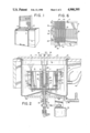
- FIG. 1 is a perspective view of an acid processor machine.
- FIG. 2 is a section view through the bowl and rotor of one form of acid processing machine which is capable of carrying a number of wafer carriers about the periphery of the rotor or turntable.
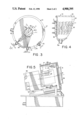
- FIG. 3 is a top plan view of the open bowl of another form of acid processor machine capable of carrying out the present invention and showing a single wafer carrier with stacked wafers located substantially concentrically of and on the rotation axis.
- FIG. 4 is a partial detail section view taken approximately at 4--4 of FIG. 3.
- FIG. 5 is an elevation view of another form of acid processor capable of carrying out the present invention and having its bowl and rotor oriented at a slight angle off horizontal so that the rotation axis is nearly horizontal.
- FIG. 6 is a detail partial side elevation view of a wafer carrier for holding wafers being processed according to the present invention.
- FIGS. 1 and 2 illustrate an acid processing machine capable of use in carrying out the method described herein, the acid processing machine 10 being of the type to mount and carry a multiplicity of wafer carriers or wafer cassettes 11 in spaced relation to the rotation axis and to carry the wafers therein orbitally around the rotation axis.
- FIGS. 3 and 4 illustrate a different type of acid processing machine which is indicated in general by the numeral 12 and which mounts such a wafer carrier 11, or 11.1 as shown, approximately on the rotation axis of the machine.
- the acid processing machine indicated by the numeral 13 is capable of being used to carry out the method set forth herein, and in this instance the wafer carrier 11 is mounted on a rotor 14 revolving about an axis 15 which is merely horizontal, but at a slight angle with the horizontal. All of these three forms of acid processor are capable of being used to carry out the method described herein.
- the machine 10 incorporates a bowl 16 which defines a processing chamber 17 which is closed by the cover 18.
- the bowl and cover are preferably made of plastic such as Teflon PFA but may be formed of stainless steel.
- the rotor 19, also of Teflon PFA or stainless steel defines a multiplicity of compartments 20, symmetrically disposed around the periphery of the rotor 19 and equidistant from the rotation axis of the rotor which is supported on a shaft 21 and mounted in bearings 22.
- the compartments 20 of the rotor 19 are tied together by a top plate 23 and a bottom plate 24 and are of such a size as to receive and confine such a wafer carrier 11 loaded with silicon wafers 25.
- the silicon wafers are arranged in a stack wherein each of the wafers is aligned with and confronts adjacent wafers, and wherein each of the wafers is oriented transversely of and normal to the rotation axis of rotor 19.
- the wafer carrier 11 and the wafers 25 therein are spaced from the rotation axis and revolve with the rotor about the rotation axis.
- the wafer carrier is slotted, apertured or foraminous in nature and has an open top 26, which comprises the front of the carrier when it is standing on end as it is mounted in the rotor 19 of the machine.
- the wafer carrier 11 which is formed of PFA Teflon, otherwise known as the perfluoroalkoxy melt processible plastic which is highly resistant to the deteriorating effect of strong chemicals such as acids, also has an open bottom 27 between the inwardly offset lower portions 28 of the carrier as to support the wafers in grooves 29 which form seats for the wafers as they are carried in the wafer carrier.
- ribs or teeth 30 which extend from the lower portion entirely upwardly throughout the sidewall so as to keep the wafers in spaced and aligned relation with each other.
- the sidewall 31 in which the teeth or ribs 30 are incorporated, are provided with a multiplicity of slots 32 to facilitate passage of etchant gas through the wafer carrier in order to obtain access to the wafers 25 confined therein.
- the wafer carrier 11 also has an end wall consisting of a crossbar 33 which may have any of a number of configurations, and may have flanges 34 for strengthening it.
- the crossbar 33 extends entirely across the wafer carrier and the sidewalls 31 may be strengthened relative to the crossbar as by gussets 35.
- a central spray post 36 extends from the cover 18 and extends downwardly at approximately the rotation axis of rotor 19 and along the wafer carrier 11 and the stack of wafers 25 therein.
- the spray post has a multiplicity of nozzles 37 therein for directing the process gases including the etchant gas onto the wafers as they revolve with the rotor in the bowl 16.
- Etchant gas and other gases are supplied through a header 37.1 which is connected to several gas lines 38, 38.1 through which gas is supplied to the nozzles 37 for spraying onto the wafers and along the full length of the stack of wafers in the bowl.
- the rotor is driven by a variable speed motor 39 which is connected to the shaft 21 as by a drive belt 40.
- the shaft 21 has a flow passage 21.1 therein for delivering fluids into the manifold pipes 42 and the nozzles 43.
- These nozzles 43 are particularly useful in directing rinsing or cleaning fluids such as deionized water for the chamber 17 when desired, and drying gas, such as nitrogen, in order to assure that the inside of the bowl 16 remains dry during processing.
- An exhaust duct 44 is provided to exhaust gases out of the chamber 17 so that a continuing flow of gas may be provided when desired.
- a drain 45 is also provided in order to remove rinsing or cleaning fluids during certain cleansing operations as may be needed.
- the wafers 25 are spaced from each other by open spaces 25.1 so that gases may pass across the faces of the wafers to accomplish the etching process.
- the wafer carrier 11 is similar to that illustrated in U.S. Pat. No. 3,961,877, but it should be understood that other similar carriers would be useful in this machine for carrying out the process described and claimed herein.
- the paricular etching process is described in considerable detail in U.S. Pat. No. 4,749,440 which is incorporated herein by reference and need not be repeated for an understanding of the present invention.
- the etchant gases are supplied through the nozzle orifices 37 and are directed toward the edges of the wafers 25 and through the spaces 25.1 between the wafers as to traverse the faces of the wafers and accomplish etching of the oxides on the faces of the wafers.
- Simultaneous etching of a multiplicity of wafers as carried in the carrier 11 is accomplished because there is a multiplicity of locations at which the gas emanates from the spray post 36, and it will be seen that the orifices 37 are arranged in a row along the face of the spray post 36.
- the wafers in the several carriers 11 spaced around the periphery of the rotor 19 will be progressively subjected to the spray of etchant gas emanating from the central spray post.
- FIGS. 3 and 4 a similar, but slightly different, form of acid processing machine is illustrated, and a slightly different form of wafer carrier, 11.1 is utilized.
- This wafer carrier 11.1 has additional slots 32.1 and 32.2 so that the sidewalls of the wafer carrier are highly foraminous as to provide minimum restriction to the flow of sprayed etchant gases.
- the wafer carriers 11 and 11.1 may be used interchangeably in the several forms of machines illustrated herein. It will be seen in the form of processing machine of FIG. 3 that the wafers 25 are supported in substantially the same manner in the wafer carrier as in FIG. 2 and the wafers revolve with the carrier 11.1 as indicated by the arrow "a" and about a rotation axis 46 which extends along and through the wafers oriented in the stack.
- the bowl 47 has a cover 48 as to close the interior chamber 49.
- Spray of the etchant gas may emanate from one or more of the nozzles 50, 51, and the diluent gases for purging the chamber may be also supplied through one of the nozzles 50, hines illustrated herein.
- the wafers 25 revolve with the carrier 11.1 as indicated by the arrow "a" and about a rotation axis 46 which extends along and through the wafers oriented in the stack.
- the bowl 47 has a cover 48 as to close the interior chamber 49.
- Spray of the etchant gas may emanate from one or more of the nozzles 50, 51, and the diluent gases for purging the chamber may be also supplied through one of the nozzles 50, films or layers that may be on the faces of the wafers.
- a duct 53 is provided for allowing the gases to escape as desired in order to provide circulation, and a drain 54 is provided to allow liquids used to clean the inside of the chamber to escape. It should be recognized however, that in the ordinary course of processing the wafers with gas phase etching, no liquid is ordinarily used or sprayed onto the wafers. However, there are some instances in which the etching will be followed by a spray of deionized water for removing particulate.
- the bowl 55 is oriented at a nearly horizontal position as to embrace the rotation axis 15 of the rotor 14.
- An openable cover 56 facilitates obtaining access into the interior 57 of the bowl or chamber.
- the wafers 25 are oriented in a stack along the rotation axis 15 and in this instance, the wafers are intersected by the rotation axis.
- Nozzles 57 in the sidewall of the bowl direct etchant gas into the chamber and toward the edges of the wafers as to traverse the faces of the wafers which are carried in the foraminous wafer carrier within the chamber.
- the rotor 14 and wafer carrier in bowl 55 is slanted slightly as to cause the wafers to be supported in the ribs within the carrier as described in connection with FIG. 2.
- a motor 58 is direct-connected to the rotor 14 to produce the necessary rotation of the rotor and the wafers carried thereby.
- the method of processing a multiplicity of semiconductor silicon wafers in an acid processing machine which is normally constructed for the use of wet etching liquids.
- the etchant gases are supplied into the chamber for traversing the faces of the wafers being processed therein.
- the method described may also be used in connection with plasmas of plasma forming gases supplied into the chamber. It may be that the rotor revolves relative to the nozzles, as illustrated, but the spraying nozzles may also be revolved around the wafer carrier carrying a stack of the wafers as to produce the necessary relative rotation between the sources of the spray gases from which the etchant gas emanates, and the wafers carried by the rotor and wafer carrier.
- the spray nozzles and the bowls and other hardware therein must be of such a nature as to resist the deteriorating effect of the strong etchant gas.
Abstract
Description
                                  TABLE 1
__________________________________________________________________________
TESTING SUMMARY
                   Oxide
                        Rotation
Test  N.sub.2
          Vapor
               Hf/ Removed
                        Speed/RPM   Particle
#  Time
      1/min.
          cc/min.
               min Δ
                        σ
                               % CV Δ
                                         Residue
__________________________________________________________________________
1  5.0'
      7.51
          3.01 125 cc
                   Cleared          2292 Yes
2  4.0'
      7.51
          3.01 125 cc
                   Cleared          2572 Yes
3  3.0'
      7.51
          3.01 125 cc
                   Cleared          1585 Yes
4  1.0'
      7.51
          3.01 375 cc
                   Cleared          678  Yes
5  20"
      7.51
          3.01 375 cc
                   269 A
                        (25)   9.3  437  No
6  20"
      7.51
          3.01 375 cc
                   243 A
                        (17.8) 7.3  311  No
7  20"
      7.51
          3.01 125 cc
                   36 A        1.7  744  No
8  20"
      7.51
          3.01 125 cc
                   21 A        0.8  554  No
9  40"
      7.51
          3.01 125 cc
                   108 A
                        (5.8)  5.4       No
10 20"
      7.51
          1.51 125 cc          No Etch
11 60"
      7.51
          1.51 125 cc
                   270  (27)   10.0      No
12 20"
      15.01
          1.51 125 cc          No Etch
13 60"
      15.01
          1.51 125 cc
                   879  (111)  12.7      Yes
14 60"
      15.01
          1.51 125 cc
                   491  (107)  21.9      Yes
__________________________________________________________________________
Claims (26)
Priority Applications (4)
| Application Number | Priority Date | Filing Date | Title |
|---|---|---|---|
| US07/334,343 US4900395A (en) | 1989-04-07 | 1989-04-07 | HF gas etching of wafers in an acid processor |
| DE69031370T DE69031370T2 (en) | 1989-04-07 | 1990-02-12 | GAS ETCHING SUBSTRATES FOR THE REMOVAL OF OXIDE LAYERS |
| EP90906011A EP0420958B1 (en) | 1989-04-07 | 1990-02-12 | Gas etching of wafers to remove oxide layers |
| PCT/US1990/000791 WO1990012419A1 (en) | 1989-04-07 | 1990-02-12 | Hf gas etching of wafers in an acid processor |
Applications Claiming Priority (1)
| Application Number | Priority Date | Filing Date | Title |
|---|---|---|---|
| US07/334,343 US4900395A (en) | 1989-04-07 | 1989-04-07 | HF gas etching of wafers in an acid processor |
Publications (1)
| Publication Number | Publication Date |
|---|---|
| US4900395A true US4900395A (en) | 1990-02-13 |
Family
ID=23306788
Family Applications (1)
| Application Number | Title | Priority Date | Filing Date |
|---|---|---|---|
| US07/334,343 Expired - Fee Related US4900395A (en) | 1989-04-07 | 1989-04-07 | HF gas etching of wafers in an acid processor |
Country Status (4)
| Country | Link |
|---|---|
| US (1) | US4900395A (en) |
| EP (1) | EP0420958B1 (en) |
| DE (1) | DE69031370T2 (en) |
| WO (1) | WO1990012419A1 (en) |
Cited By (155)
| Publication number | Priority date | Publication date | Assignee | Title |
|---|---|---|---|---|
| WO1991017967A1 (en) * | 1990-05-15 | 1991-11-28 | Semitool, Inc. | Dynamic semiconductor wafer processing using homogeneous chemical vapors |
| US5089084A (en) * | 1990-12-03 | 1992-02-18 | Micron Technology, Inc. | Hydrofluoric acid etcher and cascade rinser |
| US5112437A (en) * | 1990-02-20 | 1992-05-12 | Dainippon Screen Mfg. Co., Ltd. | Oxide film removing apparatus and removing method thereof using azeotropic vapor mixture |
| EP0529888A1 (en) * | 1991-08-22 | 1993-03-03 | AT&T Corp. | Removal of substrate perimeter material |
| US5238500A (en) * | 1990-05-15 | 1993-08-24 | Semitool, Inc. | Aqueous hydrofluoric and hydrochloric acid vapor processing of semiconductor wafers |
| US5242468A (en) * | 1991-03-19 | 1993-09-07 | Startec Ventures, Inc. | Manufacture of high precision electronic components with ultra-high purity liquids |
| US5340437A (en) * | 1993-10-08 | 1994-08-23 | Memc Electronic Materials, Inc. | Process and apparatus for etching semiconductor wafers |
| US5357991A (en) * | 1989-03-27 | 1994-10-25 | Semitool, Inc. | Gas phase semiconductor processor with liquid phase mixing |
| US5669979A (en) * | 1993-09-08 | 1997-09-23 | Uvtech Systems, Inc. | Photoreactive surface processing |
| US5814156A (en) * | 1993-09-08 | 1998-09-29 | Uvtech Systems Inc. | Photoreactive surface cleaning |
| US5820692A (en) * | 1996-01-16 | 1998-10-13 | Fsi Interntional | Vacuum compatible water vapor and rinse process module |
| US5931721A (en) * | 1994-11-07 | 1999-08-03 | Sumitomo Heavy Industries, Ltd. | Aerosol surface processing |
| US5954911A (en) * | 1995-10-12 | 1999-09-21 | Semitool, Inc. | Semiconductor processing using vapor mixtures |
| US5967156A (en) * | 1994-11-07 | 1999-10-19 | Krytek Corporation | Processing a surface |
| US6043162A (en) * | 1996-11-06 | 2000-03-28 | Asm Japan K .K. | Method of processing semiconductor substrate |
| US6147004A (en) * | 1998-07-21 | 2000-11-14 | Advanced Micro Devices, Inc. | Jet vapor reduction of the thickness of process layers |
| US6168961B1 (en) | 1998-05-21 | 2001-01-02 | Memc Electronic Materials, Inc. | Process for the preparation of epitaxial wafers for resistivity measurements |
| US20020038629A1 (en) * | 1990-05-18 | 2002-04-04 | Reardon Timothy J. | Semiconductor processing spray coating apparatus |
| US20020074013A1 (en) * | 2000-12-19 | 2002-06-20 | Applied Materials, Inc. | On-site cleaning gas generation for process chamber cleaning |
| US20020126364A1 (en) * | 1994-05-05 | 2002-09-12 | Iridigm Display Corporation, A Delaware Corporation | Interferometric modulation of radiation |
| US20030043157A1 (en) * | 1999-10-05 | 2003-03-06 | Iridigm Display Corporation | Photonic MEMS and structures |
| US20030072070A1 (en) * | 1995-05-01 | 2003-04-17 | Etalon, Inc., A Ma Corporation | Visible spectrum modulator arrays |
| US20030102019A1 (en) * | 2000-07-07 | 2003-06-05 | Semitool, Inc. | Centrifugal spray processor and retrofit kit |
| US20030109144A1 (en) * | 2000-03-27 | 2003-06-12 | Applied Materials, Inc. | Selectively etching silicon using fluorine without plasma |
| US20030121796A1 (en) * | 2001-11-26 | 2003-07-03 | Siegele Stephen H | Generation and distribution of molecular fluorine within a fabrication facility |
| US20030192569A1 (en) * | 2000-03-27 | 2003-10-16 | Applied Materials, Inc. | Fluorine process for cleaning semiconductor process chamber |
| US6674562B1 (en) | 1994-05-05 | 2004-01-06 | Iridigm Display Corporation | Interferometric modulation of radiation |
| US20040025901A1 (en) * | 2001-07-16 | 2004-02-12 | Semitool, Inc. | Stationary wafer spin/spray processor |
| US20040037768A1 (en) * | 2001-11-26 | 2004-02-26 | Robert Jackson | Method and system for on-site generation and distribution of a process gas |
| US6710908B2 (en) | 1994-05-05 | 2004-03-23 | Iridigm Display Corporation | Controlling micro-electro-mechanical cavities |
| US20040058532A1 (en) * | 2002-09-20 | 2004-03-25 | Miles Mark W. | Controlling electromechanical behavior of structures within a microelectromechanical systems device |
| US6740247B1 (en) | 1999-02-05 | 2004-05-25 | Massachusetts Institute Of Technology | HF vapor phase wafer cleaning and oxide etching |
| US20040151656A1 (en) * | 2001-11-26 | 2004-08-05 | Siegele Stephen H. | Modular molecular halogen gas generation system |
| US20050036095A1 (en) * | 2003-08-15 | 2005-02-17 | Jia-Jiun Yeh | Color-changeable pixels of an optical interference display panel |
| US20050046922A1 (en) * | 2003-09-03 | 2005-03-03 | Wen-Jian Lin | Interferometric modulation pixels and manufacturing method thereof |
| US20050078348A1 (en) * | 2003-09-30 | 2005-04-14 | Wen-Jian Lin | Structure of a micro electro mechanical system and the manufacturing method thereof |
| US20050122560A1 (en) * | 2003-12-09 | 2005-06-09 | Sampsell Jeffrey B. | Area array modulation and lead reduction in interferometric modulators |
| US20050168431A1 (en) * | 2004-02-03 | 2005-08-04 | Clarence Chui | Driver voltage adjuster |
| US20050195467A1 (en) * | 2004-03-03 | 2005-09-08 | Manish Kothari | Altering temporal response of microelectromechanical elements |
| US20050250235A1 (en) * | 2002-09-20 | 2005-11-10 | Miles Mark W | Controlling electromechanical behavior of structures within a microelectromechanical systems device |
| US20050249966A1 (en) * | 2004-05-04 | 2005-11-10 | Ming-Hau Tung | Method of manufacture for microelectromechanical devices |
| US20060001942A1 (en) * | 2004-07-02 | 2006-01-05 | Clarence Chui | Interferometric modulators with thin film transistors |
| US20060007517A1 (en) * | 2004-07-09 | 2006-01-12 | Prime View International Co., Ltd. | Structure of a micro electro mechanical system |
| US20060006138A1 (en) * | 2003-08-26 | 2006-01-12 | Wen-Jian Lin | Interference display cell and fabrication method thereof |
| US20060024880A1 (en) * | 2004-07-29 | 2006-02-02 | Clarence Chui | System and method for micro-electromechanical operation of an interferometric modulator |
| US20060065940A1 (en) * | 2004-09-27 | 2006-03-30 | Manish Kothari | Analog interferometric modulator device |
| US20060067646A1 (en) * | 2004-09-27 | 2006-03-30 | Clarence Chui | MEMS device fabricated on a pre-patterned substrate |
| US20060066543A1 (en) * | 2004-09-27 | 2006-03-30 | Gally Brian J | Ornamental display device |
| US20060066503A1 (en) * | 2004-09-27 | 2006-03-30 | Sampsell Jeffrey B | Controller and driver features for bi-stable display |
| US20060065366A1 (en) * | 2004-09-27 | 2006-03-30 | Cummings William J | Portable etch chamber |
| US20060067644A1 (en) * | 2004-09-27 | 2006-03-30 | Clarence Chui | Method of fabricating interferometric devices using lift-off processing techniques |
| US20060066876A1 (en) * | 2004-09-27 | 2006-03-30 | Manish Kothari | Method and system for sensing light using interferometric elements |
| US20060066596A1 (en) * | 2004-09-27 | 2006-03-30 | Sampsell Jeffrey B | System and method of transmitting video data |
| US20060067649A1 (en) * | 2004-09-27 | 2006-03-30 | Ming-Hau Tung | Apparatus and method for reducing slippage between structures in an interferometric modulator |
| US20060065622A1 (en) * | 2004-09-27 | 2006-03-30 | Floyd Philip D | Method and system for xenon fluoride etching with enhanced efficiency |
| US20060067651A1 (en) * | 2004-09-27 | 2006-03-30 | Clarence Chui | Photonic MEMS and structures |
| US20060066599A1 (en) * | 2004-09-27 | 2006-03-30 | Clarence Chui | Reflective display pixels arranged in non-rectangular arrays |
| US20060067650A1 (en) * | 2004-09-27 | 2006-03-30 | Clarence Chui | Method of making a reflective display device using thin film transistor production techniques |
| US20060066595A1 (en) * | 2004-09-27 | 2006-03-30 | Sampsell Jeffrey B | Method and system for driving a bi-stable display |
| US20060067643A1 (en) * | 2004-09-27 | 2006-03-30 | Clarence Chui | System and method for multi-level brightness in interferometric modulation |
| US20060066932A1 (en) * | 2004-09-27 | 2006-03-30 | Clarence Chui | Method of selective etching using etch stop layer |
| US20060066504A1 (en) * | 2004-09-27 | 2006-03-30 | Sampsell Jeffrey B | System with server based control of client device display features |
| US20060077507A1 (en) * | 2004-09-27 | 2006-04-13 | Clarence Chui | Conductive bus structure for interferometric modulator array |
| US20060077528A1 (en) * | 2004-09-27 | 2006-04-13 | Floyd Philip D | Device and method for modifying actuation voltage thresholds of a deformable membrane in an interferometric modulator |
| US20060077519A1 (en) * | 2004-09-27 | 2006-04-13 | Floyd Philip D | System and method for providing thermal compensation for an interferometric modulator display |
| US20060077504A1 (en) * | 2004-09-27 | 2006-04-13 | Floyd Philip D | Method and device for protecting interferometric modulators from electrostatic discharge |
| US20060077510A1 (en) * | 2004-09-27 | 2006-04-13 | Clarence Chui | System and method of illuminating interferometric modulators using backlighting |
| US20060077521A1 (en) * | 2004-09-27 | 2006-04-13 | Gally Brian J | System and method of implementation of interferometric modulators for display mirrors |
| US20060079048A1 (en) * | 2004-09-27 | 2006-04-13 | Sampsell Jeffrey B | Method of making prestructure for MEMS systems |
| US20060077502A1 (en) * | 2004-09-27 | 2006-04-13 | Ming-Hau Tung | Methods of fabricating interferometric modulators by selectively removing a material |
| US20060077152A1 (en) * | 2004-09-27 | 2006-04-13 | Clarence Chui | Device and method for manipulation of thermal response in a modulator |
| US20060077529A1 (en) * | 2004-09-27 | 2006-04-13 | Clarence Chui | Method of fabricating a free-standing microstructure |
| US20060077151A1 (en) * | 2004-09-27 | 2006-04-13 | Clarence Chui | Method and device for a display having transparent components integrated therein |
| US20060077155A1 (en) * | 2004-09-27 | 2006-04-13 | Clarence Chui | Reflective display device having viewable display on both sides |
| US20060077508A1 (en) * | 2004-09-27 | 2006-04-13 | Clarence Chui | Method and device for multistate interferometric light modulation |
| US20060077514A1 (en) * | 2004-09-27 | 2006-04-13 | Sampsell Jeffrey B | System and method of reducing color shift in a display |
| US20060077518A1 (en) * | 2004-09-27 | 2006-04-13 | Clarence Chui | Mirror and mirror layer for optical modulator and method |
| US20060077515A1 (en) * | 2004-09-27 | 2006-04-13 | Cummings William J | Method and device for corner interferometric modulation |
| US20060077516A1 (en) * | 2004-09-27 | 2006-04-13 | Manish Kothari | Device having a conductive light absorbing mask and method for fabricating same |
| US20060077527A1 (en) * | 2004-09-27 | 2006-04-13 | Cummings William J | Methods and devices for inhibiting tilting of a mirror in an interferometric modulator |
| US20060077156A1 (en) * | 2004-09-27 | 2006-04-13 | Clarence Chui | MEMS device having deformable membrane characterized by mechanical persistence |
| US20060077617A1 (en) * | 2004-09-27 | 2006-04-13 | Floyd Philip D | Selectable capacitance circuit |
| US20060176241A1 (en) * | 2004-09-27 | 2006-08-10 | Sampsell Jeffrey B | System and method of transmitting video data |
| US20060177950A1 (en) * | 2005-02-04 | 2006-08-10 | Wen-Jian Lin | Method of manufacturing optical interferance color display |
| US20060198013A1 (en) * | 2004-03-05 | 2006-09-07 | Sampsell Jeffrey B | Integrated modulator illumination |
| US7123216B1 (en) | 1994-05-05 | 2006-10-17 | Idc, Llc | Photonic MEMS and structures |
| US20060257070A1 (en) * | 2003-05-26 | 2006-11-16 | Wen-Jian Lin | Optical interference display cell and method of making the same |
| US20060256420A1 (en) * | 2003-06-24 | 2006-11-16 | Miles Mark W | Film stack for manufacturing micro-electromechanical systems (MEMS) devices |
| US7138984B1 (en) | 2001-06-05 | 2006-11-21 | Idc, Llc | Directly laminated touch sensitive screen |
| US20060262380A1 (en) * | 1998-04-08 | 2006-11-23 | Idc, Llc A Delaware Limited Liability Company | MEMS devices with stiction bumps |
| US20070019922A1 (en) * | 2005-07-22 | 2007-01-25 | Teruo Sasagawa | Support structure for MEMS device and methods therefor |
| US7172915B2 (en) | 2003-01-29 | 2007-02-06 | Qualcomm Mems Technologies Co., Ltd. | Optical-interference type display panel and method for making the same |
| US20070058095A1 (en) * | 1994-05-05 | 2007-03-15 | Miles Mark W | System and method for charge control in a MEMS device |
| US20070096300A1 (en) * | 2005-10-28 | 2007-05-03 | Hsin-Fu Wang | Diffusion barrier layer for MEMS devices |
| US20070155051A1 (en) * | 2005-12-29 | 2007-07-05 | Chun-Ming Wang | Method of creating MEMS device cavities by a non-etching process |
| US20070170540A1 (en) * | 2006-01-18 | 2007-07-26 | Chung Won Suk | Silicon-rich silicon nitrides as etch stops in MEMS manufature |
| US7250315B2 (en) | 2002-02-12 | 2007-07-31 | Idc, Llc | Method for fabricating a structure for a microelectromechanical system (MEMS) device |
| US20070189654A1 (en) * | 2006-01-13 | 2007-08-16 | Lasiter Jon B | Interconnect structure for MEMS device |
| US20070194414A1 (en) * | 2006-02-21 | 2007-08-23 | Chen-Jean Chou | Method for providing and removing discharging interconnect for chip-on-glass output leads and structures thereof |
| US20070196944A1 (en) * | 2006-02-22 | 2007-08-23 | Chen-Jean Chou | Electrical conditioning of MEMS device and insulating layer thereof |
| US20070194630A1 (en) * | 2006-02-23 | 2007-08-23 | Marc Mignard | MEMS device having a layer movable at asymmetric rates |
| US20070206267A1 (en) * | 2006-03-02 | 2007-09-06 | Ming-Hau Tung | Methods for producing MEMS with protective coatings using multi-component sacrificial layers |
| US20070228156A1 (en) * | 2006-03-28 | 2007-10-04 | Household Corporation | Interoperability facilitator |
| US20070236774A1 (en) * | 2006-04-10 | 2007-10-11 | Evgeni Gousev | Interferometric optical display system with broadband characteristics |
| US20070242008A1 (en) * | 2006-04-17 | 2007-10-18 | William Cummings | Mode indicator for interferometric modulator displays |
| US20070247696A1 (en) * | 2006-04-19 | 2007-10-25 | Teruo Sasagawa | Microelectromechanical device and method utilizing a porous surface |
| US20070249079A1 (en) * | 2006-04-19 | 2007-10-25 | Teruo Sasagawa | Non-planar surface structures and process for microelectromechanical systems |
| US20070247401A1 (en) * | 2006-04-19 | 2007-10-25 | Teruo Sasagawa | Microelectromechanical device and method utilizing nanoparticles |
| US20070249078A1 (en) * | 2006-04-19 | 2007-10-25 | Ming-Hau Tung | Non-planar surface structures and process for microelectromechanical systems |
| US20070258123A1 (en) * | 2006-05-03 | 2007-11-08 | Gang Xu | Electrode and interconnect materials for MEMS devices |
| US7297471B1 (en) | 2003-04-15 | 2007-11-20 | Idc, Llc | Method for manufacturing an array of interferometric modulators |
| US20070279730A1 (en) * | 2006-06-01 | 2007-12-06 | David Heald | Process and structure for fabrication of mems device having isolated egde posts |
| US20070279729A1 (en) * | 2006-06-01 | 2007-12-06 | Manish Kothari | Analog interferometric modulator device with electrostatic actuation and release |
| US20070279753A1 (en) * | 2006-06-01 | 2007-12-06 | Ming-Hau Tung | Patterning of mechanical layer in MEMS to reduce stresses at supports |
| US20070290961A1 (en) * | 2006-06-15 | 2007-12-20 | Sampsell Jeffrey B | Method and apparatus for low range bit depth enhancement for MEMS display architectures |
| US20080003710A1 (en) * | 2006-06-28 | 2008-01-03 | Lior Kogut | Support structure for free-standing MEMS device and methods for forming the same |
| US20080025849A1 (en) * | 2006-07-31 | 2008-01-31 | Hitachi, Ltd. | High-Pressure Fuel Pump Control Apparatus for an Internal Combustion Engine |
| US7327510B2 (en) | 2004-09-27 | 2008-02-05 | Idc, Llc | Process for modifying offset voltage characteristics of an interferometric modulator |
| US20080032439A1 (en) * | 2006-08-02 | 2008-02-07 | Xiaoming Yan | Selective etching of MEMS using gaseous halides and reactive co-etchants |
| US20080036795A1 (en) * | 1994-05-05 | 2008-02-14 | Idc, Llc | Method and device for modulating light |
| US20080043315A1 (en) * | 2006-08-15 | 2008-02-21 | Cummings William J | High profile contacts for microelectromechanical systems |
| US20080055707A1 (en) * | 2006-06-28 | 2008-03-06 | Lior Kogut | Support structure for free-standing MEMS device and methods for forming the same |
| US20080088908A1 (en) * | 1994-05-05 | 2008-04-17 | Idc, Llc | System and method for a mems device |
| US20080231931A1 (en) * | 2007-03-21 | 2008-09-25 | Qualcomm Incorporated | Mems cavity-coating layers and methods |
| US20080279498A1 (en) * | 2007-05-11 | 2008-11-13 | Qualcomm Incorporated | Mems structures, methods of fabricating mems components on separate substrates and assembly of same |
| US7460291B2 (en) | 1994-05-05 | 2008-12-02 | Idc, Llc | Separable modulator |
| US20080318344A1 (en) * | 2007-06-22 | 2008-12-25 | Qualcomm Incorporated | INDICATION OF THE END-POINT REACTION BETWEEN XeF2 AND MOLYBDENUM |
| US20090001524A1 (en) * | 2001-11-26 | 2009-01-01 | Siegele Stephen H | Generation and distribution of a fluorine gas |
| US7527996B2 (en) | 2006-04-19 | 2009-05-05 | Qualcomm Mems Technologies, Inc. | Non-planar surface structures and process for microelectromechanical systems |
| US7527998B2 (en) | 2006-06-30 | 2009-05-05 | Qualcomm Mems Technologies, Inc. | Method of manufacturing MEMS devices providing air gap control |
| US7532377B2 (en) | 1998-04-08 | 2009-05-12 | Idc, Llc | Movable micro-electromechanical device |
| US20100039370A1 (en) * | 1996-12-19 | 2010-02-18 | Idc, Llc | Method of making a light modulating display device and associated transistor circuitry and structures thereof |
| US7684104B2 (en) | 2004-09-27 | 2010-03-23 | Idc, Llc | MEMS using filler material and method |
| US20100079847A1 (en) * | 2008-09-30 | 2010-04-01 | Qualcomm Mems Technologies, Inc. | Multi-thickness layers for mems and mask-saving sequence for same |
| US20100149627A1 (en) * | 2005-07-22 | 2010-06-17 | Qualcomm Mems Technologies, Inc. | Support structure for mems device and methods therefor |
| US7763546B2 (en) | 2006-08-02 | 2010-07-27 | Qualcomm Mems Technologies, Inc. | Methods for reducing surface charges during the manufacture of microelectromechanical systems devices |
| US20100200938A1 (en) * | 2005-08-19 | 2010-08-12 | Qualcomm Mems Technologies, Inc. | Methods for forming layers within a mems device using liftoff processes |
| US20100245977A1 (en) * | 2009-03-27 | 2010-09-30 | Qualcomm Mems Technologies, Inc. | Post-release adjustment of interferometric modulator reflectivity |
| US20100245980A1 (en) * | 1996-11-05 | 2010-09-30 | Qualcomm Mems Technologies, Inc. | System and method for a mems device |
| US7808703B2 (en) | 2004-09-27 | 2010-10-05 | Qualcomm Mems Technologies, Inc. | System and method for implementation of interferometric modulator displays |
| US20100295138A1 (en) * | 2009-05-20 | 2010-11-25 | Baolab Microsystems Sl | Methods and systems for fabrication of mems cmos devices |
| USRE42119E1 (en) | 2002-02-27 | 2011-02-08 | Qualcomm Mems Technologies, Inc. | Microelectrochemical systems device and method for fabricating same |
| US7893919B2 (en) | 2004-09-27 | 2011-02-22 | Qualcomm Mems Technologies, Inc. | Display region architectures |
| US7898722B2 (en) | 1995-05-01 | 2011-03-01 | Qualcomm Mems Technologies, Inc. | Microelectromechanical device with restoring electrode |
| US20110051224A1 (en) * | 2008-06-05 | 2011-03-03 | Qualcomm Mems Technologies, Inc. | Low temperature amorphous silicon sacrificial layer for controlled adhesion in mems devices |
| CN102237435A (en) * | 2010-04-21 | 2011-11-09 | 陕西众森电能科技有限公司 | Edge removing method for solar cell |
| US8659816B2 (en) | 2011-04-25 | 2014-02-25 | Qualcomm Mems Technologies, Inc. | Mechanical layer and methods of making the same |
| US8817357B2 (en) | 2010-04-09 | 2014-08-26 | Qualcomm Mems Technologies, Inc. | Mechanical layer and methods of forming the same |
| US8885244B2 (en) | 2004-09-27 | 2014-11-11 | Qualcomm Mems Technologies, Inc. | Display device |
| US8928967B2 (en) | 1998-04-08 | 2015-01-06 | Qualcomm Mems Technologies, Inc. | Method and device for modulating light |
| US8963159B2 (en) | 2011-04-04 | 2015-02-24 | Qualcomm Mems Technologies, Inc. | Pixel via and methods of forming the same |
| US9001412B2 (en) | 2004-09-27 | 2015-04-07 | Qualcomm Mems Technologies, Inc. | Electromechanical device with optical function separated from mechanical and electrical function |
| US9134527B2 (en) | 2011-04-04 | 2015-09-15 | Qualcomm Mems Technologies, Inc. | Pixel via and methods of forming the same |
| US9664017B2 (en) | 2013-08-29 | 2017-05-30 | Halliburton Energy Services, Inc. | Methods and systems for generating reactive fluoride species from a gaseous precursor in a subterranean formation for stimulation thereof |
| WO2020010357A1 (en) * | 2018-07-06 | 2020-01-09 | Oem Group, Llc | Systems and methods for a spray measurement apparatus |
Families Citing this family (1)
| Publication number | Priority date | Publication date | Assignee | Title |
|---|---|---|---|---|
| JP2833946B2 (en) * | 1992-12-08 | 1998-12-09 | 日本電気株式会社 | Etching method and apparatus |
Citations (12)
| Publication number | Priority date | Publication date | Assignee | Title |
|---|---|---|---|---|
| US3879597A (en) * | 1974-08-16 | 1975-04-22 | Int Plasma Corp | Plasma etching device and process |
| US3923568A (en) * | 1974-01-14 | 1975-12-02 | Int Plasma Corp | Dry plasma process for etching noble metal |
| US3961877A (en) * | 1974-09-11 | 1976-06-08 | Fluoroware, Inc. | Reinforced wafer basket |
| US3990462A (en) * | 1975-05-19 | 1976-11-09 | Fluoroware Systems Corporation | Substrate stripping and cleaning apparatus |
| US4230515A (en) * | 1978-07-27 | 1980-10-28 | Davis & Wilder, Inc. | Plasma etching apparatus |
| US4285800A (en) * | 1979-04-18 | 1981-08-25 | Branson International Plasma Corp. | Gas plasma reactor for circuit boards and the like |
| US4303467A (en) * | 1977-11-11 | 1981-12-01 | Branson International Plasma Corporation | Process and gas for treatment of semiconductor devices |
| US4609575A (en) * | 1984-07-02 | 1986-09-02 | Fsi Corporation | Method of apparatus for applying chemicals to substrates in an acid processing system |
| US4682614A (en) * | 1985-07-26 | 1987-07-28 | Fsi Corporation | Wafer processing machine |
| US4682615A (en) * | 1984-07-02 | 1987-07-28 | Fsi Corporation | Rinsing in acid processing of substrates |
| US4691722A (en) * | 1984-08-01 | 1987-09-08 | Fsi Corporation | Bowl for liquid spray processing machine |
| US4749440A (en) * | 1985-08-28 | 1988-06-07 | Fsi Corporation | Gaseous process and apparatus for removing films from substrates |
-
1989
- 1989-04-07 US US07/334,343 patent/US4900395A/en not_active Expired - Fee Related
-
1990
- 1990-02-12 WO PCT/US1990/000791 patent/WO1990012419A1/en active IP Right Grant
- 1990-02-12 DE DE69031370T patent/DE69031370T2/en not_active Expired - Fee Related
- 1990-02-12 EP EP90906011A patent/EP0420958B1/en not_active Expired - Lifetime
Patent Citations (13)
| Publication number | Priority date | Publication date | Assignee | Title |
|---|---|---|---|---|
| US3923568A (en) * | 1974-01-14 | 1975-12-02 | Int Plasma Corp | Dry plasma process for etching noble metal |
| US3879597A (en) * | 1974-08-16 | 1975-04-22 | Int Plasma Corp | Plasma etching device and process |
| US3961877A (en) * | 1974-09-11 | 1976-06-08 | Fluoroware, Inc. | Reinforced wafer basket |
| US3961877B1 (en) * | 1974-09-11 | 1987-11-03 | ||
| US3990462A (en) * | 1975-05-19 | 1976-11-09 | Fluoroware Systems Corporation | Substrate stripping and cleaning apparatus |
| US4303467A (en) * | 1977-11-11 | 1981-12-01 | Branson International Plasma Corporation | Process and gas for treatment of semiconductor devices |
| US4230515A (en) * | 1978-07-27 | 1980-10-28 | Davis & Wilder, Inc. | Plasma etching apparatus |
| US4285800A (en) * | 1979-04-18 | 1981-08-25 | Branson International Plasma Corp. | Gas plasma reactor for circuit boards and the like |
| US4609575A (en) * | 1984-07-02 | 1986-09-02 | Fsi Corporation | Method of apparatus for applying chemicals to substrates in an acid processing system |
| US4682615A (en) * | 1984-07-02 | 1987-07-28 | Fsi Corporation | Rinsing in acid processing of substrates |
| US4691722A (en) * | 1984-08-01 | 1987-09-08 | Fsi Corporation | Bowl for liquid spray processing machine |
| US4682614A (en) * | 1985-07-26 | 1987-07-28 | Fsi Corporation | Wafer processing machine |
| US4749440A (en) * | 1985-08-28 | 1988-06-07 | Fsi Corporation | Gaseous process and apparatus for removing films from substrates |
Non-Patent Citations (2)
| Title |
|---|
| IBM Technical Disclosure Bulletin, vol. 19, No. 7, Dec., 1976 Etching of SiO 2 in Gaseous HF/H 2 O, Authors: K. D. Beyer and M. H. Whitehill. * |
| IBM Technical Disclosure Bulletin, vol. 19, No. 7, Dec., 1976 Etching of SiO2 in Gaseous HF/H2 O, Authors: K. D. Beyer and M. H. Whitehill. |
Cited By (331)
| Publication number | Priority date | Publication date | Assignee | Title |
|---|---|---|---|---|
| US5357991A (en) * | 1989-03-27 | 1994-10-25 | Semitool, Inc. | Gas phase semiconductor processor with liquid phase mixing |
| US5112437A (en) * | 1990-02-20 | 1992-05-12 | Dainippon Screen Mfg. Co., Ltd. | Oxide film removing apparatus and removing method thereof using azeotropic vapor mixture |
| WO1991017967A1 (en) * | 1990-05-15 | 1991-11-28 | Semitool, Inc. | Dynamic semiconductor wafer processing using homogeneous chemical vapors |
| US5232511A (en) * | 1990-05-15 | 1993-08-03 | Semitool, Inc. | Dynamic semiconductor wafer processing using homogeneous mixed acid vapors |
| US5238500A (en) * | 1990-05-15 | 1993-08-24 | Semitool, Inc. | Aqueous hydrofluoric and hydrochloric acid vapor processing of semiconductor wafers |
| US20020038629A1 (en) * | 1990-05-18 | 2002-04-04 | Reardon Timothy J. | Semiconductor processing spray coating apparatus |
| US5089084A (en) * | 1990-12-03 | 1992-02-18 | Micron Technology, Inc. | Hydrofluoric acid etcher and cascade rinser |
| US5242468A (en) * | 1991-03-19 | 1993-09-07 | Startec Ventures, Inc. | Manufacture of high precision electronic components with ultra-high purity liquids |
| USRE36290E (en) * | 1991-03-19 | 1999-09-07 | Air Liquide Electronics Chemicals & Services, Inc. | Manufacture of high precision electronic components with ultra-high purity liquids |
| USRE37972E1 (en) * | 1991-03-19 | 2003-02-04 | American Air Liquide, Inc. | Manufacture of high precision electronic components with ultra-high purity liquids |
| EP0529888A1 (en) * | 1991-08-22 | 1993-03-03 | AT&T Corp. | Removal of substrate perimeter material |
| US5425846A (en) * | 1991-08-22 | 1995-06-20 | At&T Corp. | Removal of substrate perimeter material |
| US5814156A (en) * | 1993-09-08 | 1998-09-29 | Uvtech Systems Inc. | Photoreactive surface cleaning |
| US5669979A (en) * | 1993-09-08 | 1997-09-23 | Uvtech Systems, Inc. | Photoreactive surface processing |
| US5340437A (en) * | 1993-10-08 | 1994-08-23 | Memc Electronic Materials, Inc. | Process and apparatus for etching semiconductor wafers |
| US6867896B2 (en) | 1994-05-05 | 2005-03-15 | Idc, Llc | Interferometric modulation of radiation |
| US7379227B2 (en) | 1994-05-05 | 2008-05-27 | Idc, Llc | Method and device for modulating light |
| US8105496B2 (en) | 1994-05-05 | 2012-01-31 | Qualcomm Mems Technologies, Inc. | Method of fabricating MEMS devices (such as IMod) comprising using a gas phase etchant to remove a layer |
| US7280265B2 (en) | 1994-05-05 | 2007-10-09 | Idc, Llc | Interferometric modulation of radiation |
| US20070229936A1 (en) * | 1994-05-05 | 2007-10-04 | Idc, Llc | Method of making a light modulating display device and associated transistor circuitry and structures thereof |
| US20080036795A1 (en) * | 1994-05-05 | 2008-02-14 | Idc, Llc | Method and device for modulating light |
| US7800809B2 (en) | 1994-05-05 | 2010-09-21 | Qualcomm Mems Technologies, Inc. | System and method for a MEMS device |
| US8059326B2 (en) | 1994-05-05 | 2011-11-15 | Qualcomm Mems Technologies Inc. | Display devices comprising of interferometric modulator and sensor |
| US8014059B2 (en) | 1994-05-05 | 2011-09-06 | Qualcomm Mems Technologies, Inc. | System and method for charge control in a MEMS device |
| US20080084601A1 (en) * | 1994-05-05 | 2008-04-10 | Idc, Llc. | System and method for a mems device |
| US20020126364A1 (en) * | 1994-05-05 | 2002-09-12 | Iridigm Display Corporation, A Delaware Corporation | Interferometric modulation of radiation |
| US7012732B2 (en) | 1994-05-05 | 2006-03-14 | Idc, Llc | Method and device for modulating light with a time-varying signal |
| US20080088908A1 (en) * | 1994-05-05 | 2008-04-17 | Idc, Llc | System and method for a mems device |
| US20110043891A1 (en) * | 1994-05-05 | 2011-02-24 | Qualcomm Mems Technologies, Inc. | Method for modulating light |
| US7372619B2 (en) | 1994-05-05 | 2008-05-13 | Idc, Llc | Display device having a movable structure for modulating light and method thereof |
| US7839556B2 (en) | 1994-05-05 | 2010-11-23 | Qualcomm Mems Technologies, Inc. | Method and device for modulating light |
| US7460291B2 (en) | 1994-05-05 | 2008-12-02 | Idc, Llc | Separable modulator |
| US7848004B2 (en) | 1994-05-05 | 2010-12-07 | Qualcomm Mems Technologies, Inc. | System and method for a MEMS device |
| US6674562B1 (en) | 1994-05-05 | 2004-01-06 | Iridigm Display Corporation | Interferometric modulation of radiation |
| US6680792B2 (en) | 1994-05-05 | 2004-01-20 | Iridigm Display Corporation | Interferometric modulation of radiation |
| US20070058095A1 (en) * | 1994-05-05 | 2007-03-15 | Miles Mark W | System and method for charge control in a MEMS device |
| US20060274074A1 (en) * | 1994-05-05 | 2006-12-07 | Miles Mark W | Display device having a movable structure for modulating light and method thereof |
| US6710908B2 (en) | 1994-05-05 | 2004-03-23 | Iridigm Display Corporation | Controlling micro-electro-mechanical cavities |
| US7692844B2 (en) | 1994-05-05 | 2010-04-06 | Qualcomm Mems Technologies, Inc. | Interferometric modulation of radiation |
| US7123216B1 (en) | 1994-05-05 | 2006-10-17 | Idc, Llc | Photonic MEMS and structures |
| US7532381B2 (en) | 1994-05-05 | 2009-05-12 | Idc, Llc | Method of making a light modulating display device and associated transistor circuitry and structures thereof |
| US20050244949A1 (en) * | 1994-05-05 | 2005-11-03 | Miles Mark W | Method and device for modulating light |
| US7042643B2 (en) | 1994-05-05 | 2006-05-09 | Idc, Llc | Interferometric modulation of radiation |
| US20050231790A1 (en) * | 1994-05-05 | 2005-10-20 | Miles Mark W | Method and device for modulating light with a time-varying signal |
| US5967156A (en) * | 1994-11-07 | 1999-10-19 | Krytek Corporation | Processing a surface |
| US5931721A (en) * | 1994-11-07 | 1999-08-03 | Sumitomo Heavy Industries, Ltd. | Aerosol surface processing |
| US6203406B1 (en) | 1994-11-07 | 2001-03-20 | Sumitomo Heavy Industries, Ltd. | Aerosol surface processing |
| US7126738B2 (en) | 1995-05-01 | 2006-10-24 | Idc, Llc | Visible spectrum modulator arrays |
| US7236284B2 (en) | 1995-05-01 | 2007-06-26 | Idc, Llc | Photonic MEMS and structures |
| US20060033975A1 (en) * | 1995-05-01 | 2006-02-16 | Miles Mark W | Photonic MEMS and structures |
| US7898722B2 (en) | 1995-05-01 | 2011-03-01 | Qualcomm Mems Technologies, Inc. | Microelectromechanical device with restoring electrode |
| US20050213183A9 (en) * | 1995-05-01 | 2005-09-29 | Iridigm Display Corporation, A Delaware Corporation | Visible spectrum modulator arrays |
| US20030072070A1 (en) * | 1995-05-01 | 2003-04-17 | Etalon, Inc., A Ma Corporation | Visible spectrum modulator arrays |
| US20060139723A9 (en) * | 1995-05-01 | 2006-06-29 | Iridigm Display Corporation, A Delaware Corporation | Visible spectrum modulator arrays |
| US5954911A (en) * | 1995-10-12 | 1999-09-21 | Semitool, Inc. | Semiconductor processing using vapor mixtures |
| US6319841B1 (en) * | 1995-10-12 | 2001-11-20 | Semitool, Inc. | Semiconductor processing using vapor mixtures |
| US5820692A (en) * | 1996-01-16 | 1998-10-13 | Fsi Interntional | Vacuum compatible water vapor and rinse process module |
| US20100245980A1 (en) * | 1996-11-05 | 2010-09-30 | Qualcomm Mems Technologies, Inc. | System and method for a mems device |
| US7929197B2 (en) | 1996-11-05 | 2011-04-19 | Qualcomm Mems Technologies, Inc. | System and method for a MEMS device |
| US6043162A (en) * | 1996-11-06 | 2000-03-28 | Asm Japan K .K. | Method of processing semiconductor substrate |
| US20100039370A1 (en) * | 1996-12-19 | 2010-02-18 | Idc, Llc | Method of making a light modulating display device and associated transistor circuitry and structures thereof |
| US7830588B2 (en) | 1996-12-19 | 2010-11-09 | Qualcomm Mems Technologies, Inc. | Method of making a light modulating display device and associated transistor circuitry and structures thereof |
| US7511875B2 (en) | 1998-04-08 | 2009-03-31 | Idc, Llc | Moveable micro-electromechanical device |
| US20070139758A1 (en) * | 1998-04-08 | 2007-06-21 | Miles Mark W | Moveable micro-electromechanical device |
| US8928967B2 (en) | 1998-04-08 | 2015-01-06 | Qualcomm Mems Technologies, Inc. | Method and device for modulating light |
| US7301704B2 (en) | 1998-04-08 | 2007-11-27 | Iridigin Display Corporation | Moveable micro-electromechanical device |
| US20090135463A1 (en) * | 1998-04-08 | 2009-05-28 | Idc, Llc | Moveable micro-electromechanical device |
| US7532377B2 (en) | 1998-04-08 | 2009-05-12 | Idc, Llc | Movable micro-electromechanical device |
| US20060262380A1 (en) * | 1998-04-08 | 2006-11-23 | Idc, Llc A Delaware Limited Liability Company | MEMS devices with stiction bumps |
| US7791787B2 (en) | 1998-04-08 | 2010-09-07 | Qualcomm Mems Technologies, Inc. | Moveable micro-electromechanical device |
| US20070008607A1 (en) * | 1998-04-08 | 2007-01-11 | Miles Mark W | Moveable micro-electromechanical device |
| US20110170166A1 (en) * | 1998-04-08 | 2011-07-14 | Qualcomm Mems Technologies, Inc. | Device for modulating light with multiple electrodes |
| US9110289B2 (en) | 1998-04-08 | 2015-08-18 | Qualcomm Mems Technologies, Inc. | Device for modulating light with multiple electrodes |
| US7554711B2 (en) | 1998-04-08 | 2009-06-30 | Idc, Llc. | MEMS devices with stiction bumps |
| US7872792B2 (en) | 1998-04-08 | 2011-01-18 | Qualcomm Mems Technologies, Inc. | Method and device for modulating light with multiple electrodes |
| US20070177247A1 (en) * | 1998-04-08 | 2007-08-02 | Miles Mark W | Method and device for modulating light with multiple electrodes |
| US6168961B1 (en) | 1998-05-21 | 2001-01-02 | Memc Electronic Materials, Inc. | Process for the preparation of epitaxial wafers for resistivity measurements |
| US6147004A (en) * | 1998-07-21 | 2000-11-14 | Advanced Micro Devices, Inc. | Jet vapor reduction of the thickness of process layers |
| US6165314A (en) * | 1998-07-21 | 2000-12-26 | Advanced Micron Devices, Inc. | Apparatus for performing jet vapor reduction of the thickness of process layers |
| US6740247B1 (en) | 1999-02-05 | 2004-05-25 | Massachusetts Institute Of Technology | HF vapor phase wafer cleaning and oxide etching |
| US20060250337A1 (en) * | 1999-10-05 | 2006-11-09 | Miles Mark W | Photonic MEMS and structures |
| US7110158B2 (en) | 1999-10-05 | 2006-09-19 | Idc, Llc | Photonic MEMS and structures |
| US7483197B2 (en) | 1999-10-05 | 2009-01-27 | Idc, Llc | Photonic MEMS and structures |
| US7830586B2 (en) | 1999-10-05 | 2010-11-09 | Qualcomm Mems Technologies, Inc. | Transparent thin films |
| US20030043157A1 (en) * | 1999-10-05 | 2003-03-06 | Iridigm Display Corporation | Photonic MEMS and structures |
| US6880561B2 (en) | 2000-03-27 | 2005-04-19 | Applied Materials, Inc. | Fluorine process for cleaning semiconductor process chamber |
| US20030109144A1 (en) * | 2000-03-27 | 2003-06-12 | Applied Materials, Inc. | Selectively etching silicon using fluorine without plasma |
| US20030192569A1 (en) * | 2000-03-27 | 2003-10-16 | Applied Materials, Inc. | Fluorine process for cleaning semiconductor process chamber |
| US7305999B2 (en) * | 2000-07-07 | 2007-12-11 | Semitool, Inc. | Centrifugal spray processor and retrofit kit |
| US20030102019A1 (en) * | 2000-07-07 | 2003-06-05 | Semitool, Inc. | Centrifugal spray processor and retrofit kit |
| US20020074013A1 (en) * | 2000-12-19 | 2002-06-20 | Applied Materials, Inc. | On-site cleaning gas generation for process chamber cleaning |
| US20040216768A1 (en) * | 2000-12-19 | 2004-11-04 | Quanyuan Shang | On-site cleaning gas generation for process chamber cleaning |
| US6843258B2 (en) | 2000-12-19 | 2005-01-18 | Applied Materials, Inc. | On-site cleaning gas generation for process chamber cleaning |
| US6981508B2 (en) | 2000-12-19 | 2006-01-03 | Applied Materials, Inc. | On-site cleaning gas generation for process chamber cleaning |
| US7138984B1 (en) | 2001-06-05 | 2006-11-21 | Idc, Llc | Directly laminated touch sensitive screen |
| US20040025901A1 (en) * | 2001-07-16 | 2004-02-12 | Semitool, Inc. | Stationary wafer spin/spray processor |
| US20040151656A1 (en) * | 2001-11-26 | 2004-08-05 | Siegele Stephen H. | Modular molecular halogen gas generation system |
| US20030121796A1 (en) * | 2001-11-26 | 2003-07-03 | Siegele Stephen H | Generation and distribution of molecular fluorine within a fabrication facility |
| US20040037768A1 (en) * | 2001-11-26 | 2004-02-26 | Robert Jackson | Method and system for on-site generation and distribution of a process gas |
| US20090001524A1 (en) * | 2001-11-26 | 2009-01-01 | Siegele Stephen H | Generation and distribution of a fluorine gas |
| US7250315B2 (en) | 2002-02-12 | 2007-07-31 | Idc, Llc | Method for fabricating a structure for a microelectromechanical system (MEMS) device |
| US7642110B2 (en) | 2002-02-12 | 2010-01-05 | Qualcomm Mems Technologies, Inc. | Method for fabricating a structure for a microelectromechanical systems (MEMS) device |
| US20080026328A1 (en) * | 2002-02-12 | 2008-01-31 | Idc, Llc | Method for fabricating a structure for a microelectromechanical systems (mems) device |
| USRE42119E1 (en) | 2002-02-27 | 2011-02-08 | Qualcomm Mems Technologies, Inc. | Microelectrochemical systems device and method for fabricating same |
| US20040058532A1 (en) * | 2002-09-20 | 2004-03-25 | Miles Mark W. | Controlling electromechanical behavior of structures within a microelectromechanical systems device |
| US8368124B2 (en) | 2002-09-20 | 2013-02-05 | Qualcomm Mems Technologies, Inc. | Electromechanical devices having etch barrier layers |
| US20050250235A1 (en) * | 2002-09-20 | 2005-11-10 | Miles Mark W | Controlling electromechanical behavior of structures within a microelectromechanical systems device |
| US7550794B2 (en) | 2002-09-20 | 2009-06-23 | Idc, Llc | Micromechanical systems device comprising a displaceable electrode and a charge-trapping layer |
| US8278726B2 (en) | 2002-09-20 | 2012-10-02 | Qualcomm Mems Technologies, Inc. | Controlling electromechanical behavior of structures within a microelectromechanical systems device |
| US20090323168A1 (en) * | 2002-09-20 | 2009-12-31 | Idc, Llc | Electromechanical devices and methods of fabricating same |
| US7781850B2 (en) | 2002-09-20 | 2010-08-24 | Qualcomm Mems Technologies, Inc. | Controlling electromechanical behavior of structures within a microelectromechanical systems device |
| US7172915B2 (en) | 2003-01-29 | 2007-02-06 | Qualcomm Mems Technologies Co., Ltd. | Optical-interference type display panel and method for making the same |
| US7723015B2 (en) | 2003-04-15 | 2010-05-25 | Qualcomm Mems Technologies, Inc. | Method for manufacturing an array of interferometeric modulators |
| US20070269748A1 (en) * | 2003-04-15 | 2007-11-22 | Idc, Llc. | Method for manufacturing an array of interferometric modulators |
| US7297471B1 (en) | 2003-04-15 | 2007-11-20 | Idc, Llc | Method for manufacturing an array of interferometric modulators |
| US7556917B2 (en) | 2003-04-15 | 2009-07-07 | Idc, Llc | Method for manufacturing an array of interferometric modulators |
| US7706044B2 (en) | 2003-05-26 | 2010-04-27 | Qualcomm Mems Technologies, Inc. | Optical interference display cell and method of making the same |
| US20060257070A1 (en) * | 2003-05-26 | 2006-11-16 | Wen-Jian Lin | Optical interference display cell and method of making the same |
| US20060256420A1 (en) * | 2003-06-24 | 2006-11-16 | Miles Mark W | Film stack for manufacturing micro-electromechanical systems (MEMS) devices |
| US7616369B2 (en) | 2003-06-24 | 2009-11-10 | Idc, Llc | Film stack for manufacturing micro-electromechanical systems (MEMS) devices |
| US20050036095A1 (en) * | 2003-08-15 | 2005-02-17 | Jia-Jiun Yeh | Color-changeable pixels of an optical interference display panel |
| US7485236B2 (en) | 2003-08-26 | 2009-02-03 | Qualcomm Mems Technologies, Inc. | Interference display cell and fabrication method thereof |
| US20060006138A1 (en) * | 2003-08-26 | 2006-01-12 | Wen-Jian Lin | Interference display cell and fabrication method thereof |
| US20050046922A1 (en) * | 2003-09-03 | 2005-03-03 | Wen-Jian Lin | Interferometric modulation pixels and manufacturing method thereof |
| US20050078348A1 (en) * | 2003-09-30 | 2005-04-14 | Wen-Jian Lin | Structure of a micro electro mechanical system and the manufacturing method thereof |
| US7291921B2 (en) | 2003-09-30 | 2007-11-06 | Qualcomm Mems Technologies, Inc. | Structure of a micro electro mechanical system and the manufacturing method thereof |
| US20050122560A1 (en) * | 2003-12-09 | 2005-06-09 | Sampsell Jeffrey B. | Area array modulation and lead reduction in interferometric modulators |
| US7161728B2 (en) | 2003-12-09 | 2007-01-09 | Idc, Llc | Area array modulation and lead reduction in interferometric modulators |
| US7532194B2 (en) | 2004-02-03 | 2009-05-12 | Idc, Llc | Driver voltage adjuster |
| US20050168431A1 (en) * | 2004-02-03 | 2005-08-04 | Clarence Chui | Driver voltage adjuster |
| US20050195467A1 (en) * | 2004-03-03 | 2005-09-08 | Manish Kothari | Altering temporal response of microelectromechanical elements |
| US7119945B2 (en) | 2004-03-03 | 2006-10-10 | Idc, Llc | Altering temporal response of microelectromechanical elements |
| US7706050B2 (en) | 2004-03-05 | 2010-04-27 | Qualcomm Mems Technologies, Inc. | Integrated modulator illumination |
| US7880954B2 (en) | 2004-03-05 | 2011-02-01 | Qualcomm Mems Technologies, Inc. | Integrated modulator illumination |
| US20060198013A1 (en) * | 2004-03-05 | 2006-09-07 | Sampsell Jeffrey B | Integrated modulator illumination |
| US20050249966A1 (en) * | 2004-05-04 | 2005-11-10 | Ming-Hau Tung | Method of manufacture for microelectromechanical devices |
| US7476327B2 (en) | 2004-05-04 | 2009-01-13 | Idc, Llc | Method of manufacture for microelectromechanical devices |
| US7256922B2 (en) | 2004-07-02 | 2007-08-14 | Idc, Llc | Interferometric modulators with thin film transistors |
| US20060001942A1 (en) * | 2004-07-02 | 2006-01-05 | Clarence Chui | Interferometric modulators with thin film transistors |
| US20060007517A1 (en) * | 2004-07-09 | 2006-01-12 | Prime View International Co., Ltd. | Structure of a micro electro mechanical system |
| US8115988B2 (en) | 2004-07-29 | 2012-02-14 | Qualcomm Mems Technologies, Inc. | System and method for micro-electromechanical operation of an interferometric modulator |
| US20060024880A1 (en) * | 2004-07-29 | 2006-02-02 | Clarence Chui | System and method for micro-electromechanical operation of an interferometric modulator |
| US20090022884A1 (en) * | 2004-07-29 | 2009-01-22 | Idc,Llc | System and method for micro-electromechanical operation of an interferometric modulator |
| US7567373B2 (en) | 2004-07-29 | 2009-07-28 | Idc, Llc | System and method for micro-electromechanical operation of an interferometric modulator |
| US20060077519A1 (en) * | 2004-09-27 | 2006-04-13 | Floyd Philip D | System and method for providing thermal compensation for an interferometric modulator display |
| US7893919B2 (en) | 2004-09-27 | 2011-02-22 | Qualcomm Mems Technologies, Inc. | Display region architectures |
| US20060065940A1 (en) * | 2004-09-27 | 2006-03-30 | Manish Kothari | Analog interferometric modulator device |
| US9097885B2 (en) | 2004-09-27 | 2015-08-04 | Qualcomm Mems Technologies, Inc. | Device having a conductive light absorbing mask and method for fabricating same |
| US9086564B2 (en) | 2004-09-27 | 2015-07-21 | Qualcomm Mems Technologies, Inc. | Conductive bus structure for interferometric modulator array |
| US9001412B2 (en) | 2004-09-27 | 2015-04-07 | Qualcomm Mems Technologies, Inc. | Electromechanical device with optical function separated from mechanical and electrical function |
| US7302157B2 (en) | 2004-09-27 | 2007-11-27 | Idc, Llc | System and method for multi-level brightness in interferometric modulation |
| US8970939B2 (en) | 2004-09-27 | 2015-03-03 | Qualcomm Mems Technologies, Inc. | Method and device for multistate interferometric light modulation |
| US7304784B2 (en) | 2004-09-27 | 2007-12-04 | Idc, Llc | Reflective display device having viewable display on both sides |
| US20060067646A1 (en) * | 2004-09-27 | 2006-03-30 | Clarence Chui | MEMS device fabricated on a pre-patterned substrate |
| US8885244B2 (en) | 2004-09-27 | 2014-11-11 | Qualcomm Mems Technologies, Inc. | Display device |
| US8638491B2 (en) | 2004-09-27 | 2014-01-28 | Qualcomm Mems Technologies, Inc. | Device having a conductive light absorbing mask and method for fabricating same |
| US20060066543A1 (en) * | 2004-09-27 | 2006-03-30 | Gally Brian J | Ornamental display device |
| US20060066503A1 (en) * | 2004-09-27 | 2006-03-30 | Sampsell Jeffrey B | Controller and driver features for bi-stable display |
| US20060065366A1 (en) * | 2004-09-27 | 2006-03-30 | Cummings William J | Portable etch chamber |
| US7317568B2 (en) | 2004-09-27 | 2008-01-08 | Idc, Llc | System and method of implementation of interferometric modulators for display mirrors |
| US20060067644A1 (en) * | 2004-09-27 | 2006-03-30 | Clarence Chui | Method of fabricating interferometric devices using lift-off processing techniques |
| US7321456B2 (en) | 2004-09-27 | 2008-01-22 | Idc, Llc | Method and device for corner interferometric modulation |
| US20060066876A1 (en) * | 2004-09-27 | 2006-03-30 | Manish Kothari | Method and system for sensing light using interferometric elements |
| US8040588B2 (en) | 2004-09-27 | 2011-10-18 | Qualcomm Mems Technologies, Inc. | System and method of illuminating interferometric modulators using backlighting |
| US7327510B2 (en) | 2004-09-27 | 2008-02-05 | Idc, Llc | Process for modifying offset voltage characteristics of an interferometric modulator |
| US20060066596A1 (en) * | 2004-09-27 | 2006-03-30 | Sampsell Jeffrey B | System and method of transmitting video data |
| US8008736B2 (en) | 2004-09-27 | 2011-08-30 | Qualcomm Mems Technologies, Inc. | Analog interferometric modulator device |
| US20060067649A1 (en) * | 2004-09-27 | 2006-03-30 | Ming-Hau Tung | Apparatus and method for reducing slippage between structures in an interferometric modulator |
| US7936497B2 (en) | 2004-09-27 | 2011-05-03 | Qualcomm Mems Technologies, Inc. | MEMS device having deformable membrane characterized by mechanical persistence |
| US20060065622A1 (en) * | 2004-09-27 | 2006-03-30 | Floyd Philip D | Method and system for xenon fluoride etching with enhanced efficiency |
| US7349136B2 (en) | 2004-09-27 | 2008-03-25 | Idc, Llc | Method and device for a display having transparent components integrated therein |
| US7349139B2 (en) | 2004-09-27 | 2008-03-25 | Idc, Llc | System and method of illuminating interferometric modulators using backlighting |
| US7355780B2 (en) | 2004-09-27 | 2008-04-08 | Idc, Llc | System and method of illuminating interferometric modulators using backlighting |
| US7920135B2 (en) | 2004-09-27 | 2011-04-05 | Qualcomm Mems Technologies, Inc. | Method and system for driving a bi-stable display |
| US7906353B2 (en) | 2004-09-27 | 2011-03-15 | Qualcomm Mems Technologies, Inc. | Method of fabricating interferometric devices using lift-off processing techniques |
| US7369294B2 (en) | 2004-09-27 | 2008-05-06 | Idc, Llc | Ornamental display device |
| US20060067651A1 (en) * | 2004-09-27 | 2006-03-30 | Clarence Chui | Photonic MEMS and structures |
| US7369296B2 (en) | 2004-09-27 | 2008-05-06 | Idc, Llc | Device and method for modifying actuation voltage thresholds of a deformable membrane in an interferometric modulator |
| US20060066599A1 (en) * | 2004-09-27 | 2006-03-30 | Clarence Chui | Reflective display pixels arranged in non-rectangular arrays |
| US7372613B2 (en) | 2004-09-27 | 2008-05-13 | Idc, Llc | Method and device for multistate interferometric light modulation |
| US7373026B2 (en) | 2004-09-27 | 2008-05-13 | Idc, Llc | MEMS device fabricated on a pre-patterned substrate |
| US7289259B2 (en) | 2004-09-27 | 2007-10-30 | Idc, Llc | Conductive bus structure for interferometric modulator array |
| US20060067650A1 (en) * | 2004-09-27 | 2006-03-30 | Clarence Chui | Method of making a reflective display device using thin film transistor production techniques |
| US20060066595A1 (en) * | 2004-09-27 | 2006-03-30 | Sampsell Jeffrey B | Method and system for driving a bi-stable display |
| US20060067643A1 (en) * | 2004-09-27 | 2006-03-30 | Clarence Chui | System and method for multi-level brightness in interferometric modulation |
| US7405861B2 (en) | 2004-09-27 | 2008-07-29 | Idc, Llc | Method and device for protecting interferometric modulators from electrostatic discharge |
| US20060066932A1 (en) * | 2004-09-27 | 2006-03-30 | Clarence Chui | Method of selective etching using etch stop layer |
| US20060066504A1 (en) * | 2004-09-27 | 2006-03-30 | Sampsell Jeffrey B | System with server based control of client device display features |
| US7417783B2 (en) | 2004-09-27 | 2008-08-26 | Idc, Llc | Mirror and mirror layer for optical modulator and method |
| US7420725B2 (en) | 2004-09-27 | 2008-09-02 | Idc, Llc | Device having a conductive light absorbing mask and method for fabricating same |
| US7420728B2 (en) | 2004-09-27 | 2008-09-02 | Idc, Llc | Methods of fabricating interferometric modulators by selectively removing a material |
| US20060077507A1 (en) * | 2004-09-27 | 2006-04-13 | Clarence Chui | Conductive bus structure for interferometric modulator array |
| US20060077528A1 (en) * | 2004-09-27 | 2006-04-13 | Floyd Philip D | Device and method for modifying actuation voltage thresholds of a deformable membrane in an interferometric modulator |
| US7429334B2 (en) | 2004-09-27 | 2008-09-30 | Idc, Llc | Methods of fabricating interferometric modulators by selectively removing a material |
| US7813026B2 (en) | 2004-09-27 | 2010-10-12 | Qualcomm Mems Technologies, Inc. | System and method of reducing color shift in a display |
| US7808703B2 (en) | 2004-09-27 | 2010-10-05 | Qualcomm Mems Technologies, Inc. | System and method for implementation of interferometric modulator displays |
| US20060077504A1 (en) * | 2004-09-27 | 2006-04-13 | Floyd Philip D | Method and device for protecting interferometric modulators from electrostatic discharge |
| US7460246B2 (en) | 2004-09-27 | 2008-12-02 | Idc, Llc | Method and system for sensing light using interferometric elements |
| US20060077510A1 (en) * | 2004-09-27 | 2006-04-13 | Clarence Chui | System and method of illuminating interferometric modulators using backlighting |
| US20060077521A1 (en) * | 2004-09-27 | 2006-04-13 | Gally Brian J | System and method of implementation of interferometric modulators for display mirrors |
| US20060079048A1 (en) * | 2004-09-27 | 2006-04-13 | Sampsell Jeffrey B | Method of making prestructure for MEMS systems |
| US20060077502A1 (en) * | 2004-09-27 | 2006-04-13 | Ming-Hau Tung | Methods of fabricating interferometric modulators by selectively removing a material |
| US7719500B2 (en) | 2004-09-27 | 2010-05-18 | Qualcomm Mems Technologies, Inc. | Reflective display pixels arranged in non-rectangular arrays |
| US20060077152A1 (en) * | 2004-09-27 | 2006-04-13 | Clarence Chui | Device and method for manipulation of thermal response in a modulator |
| US7130104B2 (en) | 2004-09-27 | 2006-10-31 | Idc, Llc | Methods and devices for inhibiting tilting of a mirror in an interferometric modulator |
| US7492502B2 (en) | 2004-09-27 | 2009-02-17 | Idc, Llc | Method of fabricating a free-standing microstructure |
| US20060209384A1 (en) * | 2004-09-27 | 2006-09-21 | Clarence Chui | System and method of illuminating interferometric modulators using backlighting |
| US7527995B2 (en) | 2004-09-27 | 2009-05-05 | Qualcomm Mems Technologies, Inc. | Method of making prestructure for MEMS systems |
| US20060077529A1 (en) * | 2004-09-27 | 2006-04-13 | Clarence Chui | Method of fabricating a free-standing microstructure |
| US20060077151A1 (en) * | 2004-09-27 | 2006-04-13 | Clarence Chui | Method and device for a display having transparent components integrated therein |
| US7684104B2 (en) | 2004-09-27 | 2010-03-23 | Idc, Llc | MEMS using filler material and method |
| US20060176241A1 (en) * | 2004-09-27 | 2006-08-10 | Sampsell Jeffrey B | System and method of transmitting video data |
| US20060077617A1 (en) * | 2004-09-27 | 2006-04-13 | Floyd Philip D | Selectable capacitance circuit |
| US7535466B2 (en) | 2004-09-27 | 2009-05-19 | Idc, Llc | System with server based control of client device display features |
| US20060077155A1 (en) * | 2004-09-27 | 2006-04-13 | Clarence Chui | Reflective display device having viewable display on both sides |
| US20060077156A1 (en) * | 2004-09-27 | 2006-04-13 | Clarence Chui | MEMS device having deformable membrane characterized by mechanical persistence |
| US7653371B2 (en) | 2004-09-27 | 2010-01-26 | Qualcomm Mems Technologies, Inc. | Selectable capacitance circuit |
| US20060077508A1 (en) * | 2004-09-27 | 2006-04-13 | Clarence Chui | Method and device for multistate interferometric light modulation |
| US20060077514A1 (en) * | 2004-09-27 | 2006-04-13 | Sampsell Jeffrey B | System and method of reducing color shift in a display |
| US20060076311A1 (en) * | 2004-09-27 | 2006-04-13 | Ming-Hau Tung | Methods of fabricating interferometric modulators by selectively removing a material |
| US20060077527A1 (en) * | 2004-09-27 | 2006-04-13 | Cummings William J | Methods and devices for inhibiting tilting of a mirror in an interferometric modulator |
| US7554714B2 (en) | 2004-09-27 | 2009-06-30 | Idc, Llc | Device and method for manipulation of thermal response in a modulator |
| US7553684B2 (en) | 2004-09-27 | 2009-06-30 | Idc, Llc | Method of fabricating interferometric devices using lift-off processing techniques |
| US20060077516A1 (en) * | 2004-09-27 | 2006-04-13 | Manish Kothari | Device having a conductive light absorbing mask and method for fabricating same |
| US7630119B2 (en) | 2004-09-27 | 2009-12-08 | Qualcomm Mems Technologies, Inc. | Apparatus and method for reducing slippage between structures in an interferometric modulator |
| US7564612B2 (en) | 2004-09-27 | 2009-07-21 | Idc, Llc | Photonic MEMS and structures |
| US20060077518A1 (en) * | 2004-09-27 | 2006-04-13 | Clarence Chui | Mirror and mirror layer for optical modulator and method |
| US20060077515A1 (en) * | 2004-09-27 | 2006-04-13 | Cummings William J | Method and device for corner interferometric modulation |
| US20090262412A1 (en) * | 2004-09-27 | 2009-10-22 | Idc, Llc | Method of fabricating interferometric devices using lift-off processing techniques |
| US7586484B2 (en) | 2004-09-27 | 2009-09-08 | Idc, Llc | Controller and driver features for bi-stable display |
| US20090218312A1 (en) * | 2004-09-27 | 2009-09-03 | Idc, Llc | Method and system for xenon fluoride etching with enhanced efficiency |
| US20080157413A1 (en) * | 2005-02-04 | 2008-07-03 | Qualcomm Mems Technologies, Inc. | Method of manufacturing optical interference color display |
| US20060177950A1 (en) * | 2005-02-04 | 2006-08-10 | Wen-Jian Lin | Method of manufacturing optical interferance color display |
| US7547565B2 (en) | 2005-02-04 | 2009-06-16 | Qualcomm Mems Technologies, Inc. | Method of manufacturing optical interference color display |
| US20100149627A1 (en) * | 2005-07-22 | 2010-06-17 | Qualcomm Mems Technologies, Inc. | Support structure for mems device and methods therefor |
| US20100147790A1 (en) * | 2005-07-22 | 2010-06-17 | Qualcomm Mems Technologies, Inc. | Support structure for mems device and methods therefor |
| US20070019922A1 (en) * | 2005-07-22 | 2007-01-25 | Teruo Sasagawa | Support structure for MEMS device and methods therefor |
| US8218229B2 (en) | 2005-07-22 | 2012-07-10 | Qualcomm Mems Technologies, Inc. | Support structure for MEMS device and methods therefor |
| US8149497B2 (en) | 2005-07-22 | 2012-04-03 | Qualcomm Mems Technologies, Inc. | Support structure for MEMS device and methods therefor |
| US7534640B2 (en) | 2005-07-22 | 2009-05-19 | Qualcomm Mems Technologies, Inc. | Support structure for MEMS device and methods therefor |
| US7835093B2 (en) | 2005-08-19 | 2010-11-16 | Qualcomm Mems Technologies, Inc. | Methods for forming layers within a MEMS device using liftoff processes |
| US20100202039A1 (en) * | 2005-08-19 | 2010-08-12 | Qualcomm Mems Technologies, Inc. | Mems devices having support structures with substantially vertical sidewalls and methods for fabricating the same |
| US8298847B2 (en) | 2005-08-19 | 2012-10-30 | Qualcomm Mems Technologies, Inc. | MEMS devices having support structures with substantially vertical sidewalls and methods for fabricating the same |
| US20100200938A1 (en) * | 2005-08-19 | 2010-08-12 | Qualcomm Mems Technologies, Inc. | Methods for forming layers within a mems device using liftoff processes |
| US7630114B2 (en) | 2005-10-28 | 2009-12-08 | Idc, Llc | Diffusion barrier layer for MEMS devices |
| US20070096300A1 (en) * | 2005-10-28 | 2007-05-03 | Hsin-Fu Wang | Diffusion barrier layer for MEMS devices |
| US20070155051A1 (en) * | 2005-12-29 | 2007-07-05 | Chun-Ming Wang | Method of creating MEMS device cavities by a non-etching process |
| US20100271688A1 (en) * | 2005-12-29 | 2010-10-28 | Qualcomm Mems Technologies, Inc. | Method of creating mems device cavities by a non-etching process |
| US7795061B2 (en) | 2005-12-29 | 2010-09-14 | Qualcomm Mems Technologies, Inc. | Method of creating MEMS device cavities by a non-etching process |
| US8394656B2 (en) | 2005-12-29 | 2013-03-12 | Qualcomm Mems Technologies, Inc. | Method of creating MEMS device cavities by a non-etching process |
| US7916980B2 (en) | 2006-01-13 | 2011-03-29 | Qualcomm Mems Technologies, Inc. | Interconnect structure for MEMS device |
| US20070189654A1 (en) * | 2006-01-13 | 2007-08-16 | Lasiter Jon B | Interconnect structure for MEMS device |
| US8971675B2 (en) | 2006-01-13 | 2015-03-03 | Qualcomm Mems Technologies, Inc. | Interconnect structure for MEMS device |
| US7382515B2 (en) | 2006-01-18 | 2008-06-03 | Qualcomm Mems Technologies, Inc. | Silicon-rich silicon nitrides as etch stops in MEMS manufacture |
| US8064124B2 (en) | 2006-01-18 | 2011-11-22 | Qualcomm Mems Technologies, Inc. | Silicon-rich silicon nitrides as etch stops in MEMS manufacture |
| US20080226929A1 (en) * | 2006-01-18 | 2008-09-18 | Qualcomm Mems Technologies, Inc. | Silicon-rich silicon nitrides as etch stop in mems manufacture |
| US20070170540A1 (en) * | 2006-01-18 | 2007-07-26 | Chung Won Suk | Silicon-rich silicon nitrides as etch stops in MEMS manufature |
| US20070194414A1 (en) * | 2006-02-21 | 2007-08-23 | Chen-Jean Chou | Method for providing and removing discharging interconnect for chip-on-glass output leads and structures thereof |
| US7582952B2 (en) | 2006-02-21 | 2009-09-01 | Qualcomm Mems Technologies, Inc. | Method for providing and removing discharging interconnect for chip-on-glass output leads and structures thereof |
| US7547568B2 (en) | 2006-02-22 | 2009-06-16 | Qualcomm Mems Technologies, Inc. | Electrical conditioning of MEMS device and insulating layer thereof |
| US20070196944A1 (en) * | 2006-02-22 | 2007-08-23 | Chen-Jean Chou | Electrical conditioning of MEMS device and insulating layer thereof |
| US7550810B2 (en) | 2006-02-23 | 2009-06-23 | Qualcomm Mems Technologies, Inc. | MEMS device having a layer movable at asymmetric rates |
| US20070194630A1 (en) * | 2006-02-23 | 2007-08-23 | Marc Mignard | MEMS device having a layer movable at asymmetric rates |
| US7952789B2 (en) | 2006-03-02 | 2011-05-31 | Qualcomm Mems Technologies, Inc. | MEMS devices with multi-component sacrificial layers |
| US20070206267A1 (en) * | 2006-03-02 | 2007-09-06 | Ming-Hau Tung | Methods for producing MEMS with protective coatings using multi-component sacrificial layers |
| US7450295B2 (en) | 2006-03-02 | 2008-11-11 | Qualcomm Mems Technologies, Inc. | Methods for producing MEMS with protective coatings using multi-component sacrificial layers |
| US20100165442A1 (en) * | 2006-03-02 | 2010-07-01 | Qualcomm Mems Technologies, Inc. | Mems devices with multi-component sacrificial layers |
| US20070228156A1 (en) * | 2006-03-28 | 2007-10-04 | Household Corporation | Interoperability facilitator |
| US7643203B2 (en) | 2006-04-10 | 2010-01-05 | Qualcomm Mems Technologies, Inc. | Interferometric optical display system with broadband characteristics |
| US20070236774A1 (en) * | 2006-04-10 | 2007-10-11 | Evgeni Gousev | Interferometric optical display system with broadband characteristics |
| US7903047B2 (en) | 2006-04-17 | 2011-03-08 | Qualcomm Mems Technologies, Inc. | Mode indicator for interferometric modulator displays |
| US20070242008A1 (en) * | 2006-04-17 | 2007-10-18 | William Cummings | Mode indicator for interferometric modulator displays |
| US7417784B2 (en) | 2006-04-19 | 2008-08-26 | Qualcomm Mems Technologies, Inc. | Microelectromechanical device and method utilizing a porous surface |
| US7527996B2 (en) | 2006-04-19 | 2009-05-05 | Qualcomm Mems Technologies, Inc. | Non-planar surface structures and process for microelectromechanical systems |
| US7623287B2 (en) | 2006-04-19 | 2009-11-24 | Qualcomm Mems Technologies, Inc. | Non-planar surface structures and process for microelectromechanical systems |
| US20070247696A1 (en) * | 2006-04-19 | 2007-10-25 | Teruo Sasagawa | Microelectromechanical device and method utilizing a porous surface |
| US7711239B2 (en) | 2006-04-19 | 2010-05-04 | Qualcomm Mems Technologies, Inc. | Microelectromechanical device and method utilizing nanoparticles |
| US7564613B2 (en) | 2006-04-19 | 2009-07-21 | Qualcomm Mems Technologies, Inc. | Microelectromechanical device and method utilizing a porous surface |
| US20070249079A1 (en) * | 2006-04-19 | 2007-10-25 | Teruo Sasagawa | Non-planar surface structures and process for microelectromechanical systems |
| US20070249078A1 (en) * | 2006-04-19 | 2007-10-25 | Ming-Hau Tung | Non-planar surface structures and process for microelectromechanical systems |
| US20080030825A1 (en) * | 2006-04-19 | 2008-02-07 | Qualcomm Incorporated | Microelectromechanical device and method utilizing a porous surface |
| US20070247401A1 (en) * | 2006-04-19 | 2007-10-25 | Teruo Sasagawa | Microelectromechanical device and method utilizing nanoparticles |
| US7369292B2 (en) | 2006-05-03 | 2008-05-06 | Qualcomm Mems Technologies, Inc. | Electrode and interconnect materials for MEMS devices |
| US20070258123A1 (en) * | 2006-05-03 | 2007-11-08 | Gang Xu | Electrode and interconnect materials for MEMS devices |
| US7321457B2 (en) | 2006-06-01 | 2008-01-22 | Qualcomm Incorporated | Process and structure for fabrication of MEMS device having isolated edge posts |
| US7405863B2 (en) | 2006-06-01 | 2008-07-29 | Qualcomm Mems Technologies, Inc. | Patterning of mechanical layer in MEMS to reduce stresses at supports |
| US7561321B2 (en) | 2006-06-01 | 2009-07-14 | Qualcomm Mems Technologies, Inc. | Process and structure for fabrication of MEMS device having isolated edge posts |
| US20070279753A1 (en) * | 2006-06-01 | 2007-12-06 | Ming-Hau Tung | Patterning of mechanical layer in MEMS to reduce stresses at supports |
| US20070279729A1 (en) * | 2006-06-01 | 2007-12-06 | Manish Kothari | Analog interferometric modulator device with electrostatic actuation and release |
| US20070279730A1 (en) * | 2006-06-01 | 2007-12-06 | David Heald | Process and structure for fabrication of mems device having isolated egde posts |
| US7649671B2 (en) | 2006-06-01 | 2010-01-19 | Qualcomm Mems Technologies, Inc. | Analog interferometric modulator device with electrostatic actuation and release |
| US7471442B2 (en) | 2006-06-15 | 2008-12-30 | Qualcomm Mems Technologies, Inc. | Method and apparatus for low range bit depth enhancements for MEMS display architectures |
| US20070290961A1 (en) * | 2006-06-15 | 2007-12-20 | Sampsell Jeffrey B | Method and apparatus for low range bit depth enhancement for MEMS display architectures |
| US20080055707A1 (en) * | 2006-06-28 | 2008-03-06 | Lior Kogut | Support structure for free-standing MEMS device and methods for forming the same |
| US7835061B2 (en) | 2006-06-28 | 2010-11-16 | Qualcomm Mems Technologies, Inc. | Support structures for free-standing electromechanical devices |
| US7385744B2 (en) | 2006-06-28 | 2008-06-10 | Qualcomm Mems Technologies, Inc. | Support structure for free-standing MEMS device and methods for forming the same |
| US20080003710A1 (en) * | 2006-06-28 | 2008-01-03 | Lior Kogut | Support structure for free-standing MEMS device and methods for forming the same |
| US8964280B2 (en) | 2006-06-30 | 2015-02-24 | Qualcomm Mems Technologies, Inc. | Method of manufacturing MEMS devices providing air gap control |
| US7527998B2 (en) | 2006-06-30 | 2009-05-05 | Qualcomm Mems Technologies, Inc. | Method of manufacturing MEMS devices providing air gap control |
| US20080025849A1 (en) * | 2006-07-31 | 2008-01-31 | Hitachi, Ltd. | High-Pressure Fuel Pump Control Apparatus for an Internal Combustion Engine |
| US20080032439A1 (en) * | 2006-08-02 | 2008-02-07 | Xiaoming Yan | Selective etching of MEMS using gaseous halides and reactive co-etchants |
| US7763546B2 (en) | 2006-08-02 | 2010-07-27 | Qualcomm Mems Technologies, Inc. | Methods for reducing surface charges during the manufacture of microelectromechanical systems devices |
| US7566664B2 (en) | 2006-08-02 | 2009-07-28 | Qualcomm Mems Technologies, Inc. | Selective etching of MEMS using gaseous halides and reactive co-etchants |
| US20080043315A1 (en) * | 2006-08-15 | 2008-02-21 | Cummings William J | High profile contacts for microelectromechanical systems |
| US20080231931A1 (en) * | 2007-03-21 | 2008-09-25 | Qualcomm Incorporated | Mems cavity-coating layers and methods |
| US8164815B2 (en) | 2007-03-21 | 2012-04-24 | Qualcomm Mems Technologies, Inc. | MEMS cavity-coating layers and methods |
| US7733552B2 (en) | 2007-03-21 | 2010-06-08 | Qualcomm Mems Technologies, Inc | MEMS cavity-coating layers and methods |
| US20100245979A1 (en) * | 2007-03-21 | 2010-09-30 | Qualcomm Mems Technologies, Inc. | Mems cavity-coating layers and methods |
| US8830557B2 (en) | 2007-05-11 | 2014-09-09 | Qualcomm Mems Technologies, Inc. | Methods of fabricating MEMS with spacers between plates and devices formed by same |
| US8284475B2 (en) | 2007-05-11 | 2012-10-09 | Qualcomm Mems Technologies, Inc. | Methods of fabricating MEMS with spacers between plates and devices formed by same |
| US20080279498A1 (en) * | 2007-05-11 | 2008-11-13 | Qualcomm Incorporated | Mems structures, methods of fabricating mems components on separate substrates and assembly of same |
| US7719752B2 (en) | 2007-05-11 | 2010-05-18 | Qualcomm Mems Technologies, Inc. | MEMS structures, methods of fabricating MEMS components on separate substrates and assembly of same |
| US20100182675A1 (en) * | 2007-05-11 | 2010-07-22 | Qualcomm Mems Technologies, Inc. | Methods of fabricating mems with spacers between plates and devices formed by same |
| US7569488B2 (en) | 2007-06-22 | 2009-08-04 | Qualcomm Mems Technologies, Inc. | Methods of making a MEMS device by monitoring a process parameter |
| US20080318344A1 (en) * | 2007-06-22 | 2008-12-25 | Qualcomm Incorporated | INDICATION OF THE END-POINT REACTION BETWEEN XeF2 AND MOLYBDENUM |
| US8358458B2 (en) | 2008-06-05 | 2013-01-22 | Qualcomm Mems Technologies, Inc. | Low temperature amorphous silicon sacrificial layer for controlled adhesion in MEMS devices |
| US20110051224A1 (en) * | 2008-06-05 | 2011-03-03 | Qualcomm Mems Technologies, Inc. | Low temperature amorphous silicon sacrificial layer for controlled adhesion in mems devices |
| US7719754B2 (en) | 2008-09-30 | 2010-05-18 | Qualcomm Mems Technologies, Inc. | Multi-thickness layers for MEMS and mask-saving sequence for same |
| US20100079847A1 (en) * | 2008-09-30 | 2010-04-01 | Qualcomm Mems Technologies, Inc. | Multi-thickness layers for mems and mask-saving sequence for same |
| US20100245977A1 (en) * | 2009-03-27 | 2010-09-30 | Qualcomm Mems Technologies, Inc. | Post-release adjustment of interferometric modulator reflectivity |
| US7864403B2 (en) | 2009-03-27 | 2011-01-04 | Qualcomm Mems Technologies, Inc. | Post-release adjustment of interferometric modulator reflectivity |
| US20100295138A1 (en) * | 2009-05-20 | 2010-11-25 | Baolab Microsystems Sl | Methods and systems for fabrication of mems cmos devices |
| US8817357B2 (en) | 2010-04-09 | 2014-08-26 | Qualcomm Mems Technologies, Inc. | Mechanical layer and methods of forming the same |
| CN102237435B (en) * | 2010-04-21 | 2013-12-11 | 陕西众森电能科技有限公司 | Edge removing method for solar cell |
| CN102237435A (en) * | 2010-04-21 | 2011-11-09 | 陕西众森电能科技有限公司 | Edge removing method for solar cell |
| US8963159B2 (en) | 2011-04-04 | 2015-02-24 | Qualcomm Mems Technologies, Inc. | Pixel via and methods of forming the same |
| US9134527B2 (en) | 2011-04-04 | 2015-09-15 | Qualcomm Mems Technologies, Inc. | Pixel via and methods of forming the same |
| US8659816B2 (en) | 2011-04-25 | 2014-02-25 | Qualcomm Mems Technologies, Inc. | Mechanical layer and methods of making the same |
| US9664017B2 (en) | 2013-08-29 | 2017-05-30 | Halliburton Energy Services, Inc. | Methods and systems for generating reactive fluoride species from a gaseous precursor in a subterranean formation for stimulation thereof |
| WO2020010357A1 (en) * | 2018-07-06 | 2020-01-09 | Oem Group, Llc | Systems and methods for a spray measurement apparatus |
| US10777434B2 (en) | 2018-07-06 | 2020-09-15 | Oem Group, Llc | Systems and methods for a spray measurement apparatus |
Also Published As
| Publication number | Publication date |
|---|---|
| EP0420958A1 (en) | 1991-04-10 |
| EP0420958B1 (en) | 1997-09-03 |
| WO1990012419A1 (en) | 1990-10-18 |
| DE69031370D1 (en) | 1997-10-09 |
| DE69031370T2 (en) | 1998-01-22 |
Similar Documents
| Publication | Publication Date | Title |
|---|---|---|
| US4900395A (en) | HF gas etching of wafers in an acid processor | |
| US7258124B2 (en) | Apparatus and method for treating surfaces of semiconductor wafers using ozone | |
| US7051743B2 (en) | Apparatus and method for cleaning surfaces of semiconductor wafers using ozone | |
| US6352623B1 (en) | Vertically configured chamber used for multiple processes | |
| US5100476A (en) | Method and apparatus for cleaning semiconductor devices | |
| US7021319B2 (en) | Assisted rinsing in a single wafer cleaning process | |
| US6269511B1 (en) | Surface cleaning apparatus | |
| JP2000208413A (en) | Developing device and developing treatment method | |
| US20050121053A1 (en) | Single type of semiconductor wafer cleaning apparatus and method of using the same | |
| US20110180114A1 (en) | Liquid aerosol particle removal method | |
| CN209981177U (en) | Wafer cleaning device | |
| JPS6064436A (en) | Spin drier | |
| US7494550B2 (en) | Fluid delivery ring and methods for making and implementing the same | |
| JP2016213252A (en) | Substrate liquid processing method, substrate liquid processing device and storage medium | |
| KR20060132987A (en) | Substrate brush scrubbing and proximity cleaning-drying sequence using compatible chemistries, and proximity substrate preparation sequence, and methods, apparatus, and systems for implementing the same | |
| JP3180209B2 (en) | Developing device and developing method | |
| JPH088222A (en) | Spin processor | |
| US6360756B1 (en) | Wafer rinse tank for metal etching and method for using | |
| US20040025901A1 (en) | Stationary wafer spin/spray processor | |
| US6869486B2 (en) | Methods for removing metallic contamination from wafer containers | |
| JP3100108B2 (en) | Rotary processing equipment | |
| JP2002124465A (en) | Developer | |
| JP2001351894A (en) | Wafer carrier, method of cleaning wafer, and method of manufacturing semiconductor device | |
| JP2001267279A (en) | Method and apparatus for cleaning and etching individual wafer by utilizing wet chemical phenomena | |
| KR20220160139A (en) | Apparatus for treating substrate |
Legal Events
| Date | Code | Title | Description |
|---|---|---|---|
| AS | Assignment |
Owner name: FSI INTERNATIONAL, INC., 322 LAKE HAZELTINE DRIVE, Free format text: ASSIGNMENT OF ASSIGNORS INTEREST.;ASSIGNORS:SYVERSON, DANIEL J.;NOVAK, RICHARD E.;REEL/FRAME:005061/0723 Effective date: 19890310 |
|
| AS | Assignment |
Owner name: CONGRESS FINANCIAL CORPORATION AN IL CORPORATION Free format text: SECURITY INTEREST;ASSIGNOR:FSI INTERNATIONAL, INC., A CORPORATION OF MN;REEL/FRAME:006041/0930 Effective date: 19920228 |
|
| FEPP | Fee payment procedure |
Free format text: PAYOR NUMBER ASSIGNED (ORIGINAL EVENT CODE: ASPN); ENTITY STATUS OF PATENT OWNER: LARGE ENTITY |
|
| FPAY | Fee payment |
Year of fee payment: 4 |
|
| AS | Assignment |
Owner name: FSI INTERNATIONAL, INC., MINNESOTA Free format text: RELEASE OF PATENTS;ASSIGNOR:CONGRESS FINANCIAL CORPORATION (CENTRAL);REEL/FRAME:006924/0912 Effective date: 19940318 |
|
| FEPP | Fee payment procedure |
Free format text: PAT HLDR NO LONGER CLAIMS SMALL ENT STAT AS SMALL BUSINESS (ORIGINAL EVENT CODE: LSM2); ENTITY STATUS OF PATENT OWNER: LARGE ENTITY |
|
| FPAY | Fee payment |
Year of fee payment: 8 |
|
| REMI | Maintenance fee reminder mailed | ||
| LAPS | Lapse for failure to pay maintenance fees | ||
| STCH | Information on status: patent discontinuation |
Free format text: PATENT EXPIRED DUE TO NONPAYMENT OF MAINTENANCE FEES UNDER 37 CFR 1.362 |
|
| FP | Lapsed due to failure to pay maintenance fee |
Effective date: 20020213 |