US20060198760A1 - Opto-acoustic sensor device and associated method - Google Patents
Opto-acoustic sensor device and associated method Download PDFInfo
- Publication number
- US20060198760A1 US20060198760A1 US11/391,744 US39174406A US2006198760A1 US 20060198760 A1 US20060198760 A1 US 20060198760A1 US 39174406 A US39174406 A US 39174406A US 2006198760 A1 US2006198760 A1 US 2006198760A1
- Authority
- US
- United States
- Prior art keywords
- sensor layer
- target species
- substrate
- sensor
- interaction
- Prior art date
- Legal status (The legal status is an assumption and is not a legal conclusion. Google has not performed a legal analysis and makes no representation as to the accuracy of the status listed.)
- Abandoned
Links
- 238000000034 method Methods 0.000 title claims abstract description 31
- 239000000758 substrate Substances 0.000 claims abstract description 65
- 230000003993 interaction Effects 0.000 claims abstract description 54
- 230000003287 optical effect Effects 0.000 claims abstract description 53
- 238000006243 chemical reaction Methods 0.000 claims abstract description 46
- 230000005670 electromagnetic radiation Effects 0.000 claims abstract description 43
- 230000008859 change Effects 0.000 claims abstract description 24
- 238000004891 communication Methods 0.000 claims abstract description 11
- 230000000644 propagated effect Effects 0.000 claims abstract description 5
- 239000010410 layer Substances 0.000 claims description 199
- 239000000126 substance Substances 0.000 claims description 30
- 230000004044 response Effects 0.000 claims description 23
- 239000007795 chemical reaction product Substances 0.000 claims description 18
- 239000003795 chemical substances by application Substances 0.000 claims description 16
- 230000007717 exclusion Effects 0.000 claims description 11
- VYPSYNLAJGMNEJ-UHFFFAOYSA-N silicon dioxide Inorganic materials O=[Si]=O VYPSYNLAJGMNEJ-UHFFFAOYSA-N 0.000 claims description 9
- XLOMVQKBTHCTTD-UHFFFAOYSA-N Zinc monoxide Chemical compound [Zn]=O XLOMVQKBTHCTTD-UHFFFAOYSA-N 0.000 claims description 8
- 230000010355 oscillation Effects 0.000 claims description 8
- 239000010453 quartz Substances 0.000 claims description 7
- 230000001902 propagating effect Effects 0.000 claims description 6
- 238000005415 bioluminescence Methods 0.000 claims description 5
- 230000029918 bioluminescence Effects 0.000 claims description 5
- 229910052751 metal Inorganic materials 0.000 claims description 5
- 239000002184 metal Substances 0.000 claims description 5
- 238000001069 Raman spectroscopy Methods 0.000 claims description 4
- 230000000694 effects Effects 0.000 claims description 4
- GQYHUHYESMUTHG-UHFFFAOYSA-N lithium niobate Chemical compound [Li+].[O-][Nb](=O)=O GQYHUHYESMUTHG-UHFFFAOYSA-N 0.000 claims description 4
- 102000004169 proteins and genes Human genes 0.000 claims description 4
- 108090000623 proteins and genes Proteins 0.000 claims description 4
- 239000011787 zinc oxide Substances 0.000 claims description 4
- 108091023037 Aptamer Proteins 0.000 claims description 3
- OKTJSMMVPCPJKN-UHFFFAOYSA-N Carbon Chemical compound [C] OKTJSMMVPCPJKN-UHFFFAOYSA-N 0.000 claims description 3
- 229910052799 carbon Inorganic materials 0.000 claims description 3
- 108090000765 processed proteins & peptides Proteins 0.000 claims description 3
- 150000003384 small molecules Chemical class 0.000 claims description 3
- WSMQKESQZFQMFW-UHFFFAOYSA-N 5-methyl-pyrazole-3-carboxylic acid Chemical compound CC1=CC(C(O)=O)=NN1 WSMQKESQZFQMFW-UHFFFAOYSA-N 0.000 claims description 2
- 239000011230 binding agent Substances 0.000 claims description 2
- 239000005387 chalcogenide glass Substances 0.000 claims description 2
- 229910000154 gallium phosphate Inorganic materials 0.000 claims description 2
- AMGQUBHHOARCQH-UHFFFAOYSA-N indium;oxotin Chemical compound [In].[Sn]=O AMGQUBHHOARCQH-UHFFFAOYSA-N 0.000 claims description 2
- 238000005424 photoluminescence Methods 0.000 claims description 2
- 238000002198 surface plasmon resonance spectroscopy Methods 0.000 claims description 2
- XOLBLPGZBRYERU-UHFFFAOYSA-N tin dioxide Chemical compound O=[Sn]=O XOLBLPGZBRYERU-UHFFFAOYSA-N 0.000 claims description 2
- 229910001887 tin oxide Inorganic materials 0.000 claims description 2
- 238000005390 triboluminescence Methods 0.000 claims description 2
- 108010021625 Immunoglobulin Fragments Proteins 0.000 claims 1
- 102000008394 Immunoglobulin Fragments Human genes 0.000 claims 1
- 239000000232 Lipid Bilayer Substances 0.000 claims 1
- 230000008929 regeneration Effects 0.000 claims 1
- 238000011069 regeneration method Methods 0.000 claims 1
- 239000002356 single layer Substances 0.000 claims 1
- 241000894007 species Species 0.000 description 110
- 239000000463 material Substances 0.000 description 32
- -1 polyethylene Polymers 0.000 description 30
- 239000000047 product Substances 0.000 description 24
- 238000002835 absorbance Methods 0.000 description 18
- 239000000975 dye Substances 0.000 description 15
- CSCPPACGZOOCGX-UHFFFAOYSA-N Acetone Chemical compound CC(C)=O CSCPPACGZOOCGX-UHFFFAOYSA-N 0.000 description 12
- HEMHJVSKTPXQMS-UHFFFAOYSA-M Sodium hydroxide Chemical compound [OH-].[Na+] HEMHJVSKTPXQMS-UHFFFAOYSA-M 0.000 description 11
- 239000011148 porous material Substances 0.000 description 11
- 238000001514 detection method Methods 0.000 description 10
- 150000001875 compounds Chemical class 0.000 description 9
- 238000009826 distribution Methods 0.000 description 8
- 239000011159 matrix material Substances 0.000 description 8
- 239000000203 mixture Substances 0.000 description 8
- 239000000523 sample Substances 0.000 description 8
- 238000003380 quartz crystal microbalance Methods 0.000 description 7
- GUEIZVNYDFNHJU-UHFFFAOYSA-N quinizarin Chemical compound O=C1C2=CC=CC=C2C(=O)C2=C1C(O)=CC=C2O GUEIZVNYDFNHJU-UHFFFAOYSA-N 0.000 description 7
- 235000012239 silicon dioxide Nutrition 0.000 description 7
- OKKJLVBELUTLKV-UHFFFAOYSA-N Methanol Chemical compound OC OKKJLVBELUTLKV-UHFFFAOYSA-N 0.000 description 6
- KWYUFKZDYYNOTN-UHFFFAOYSA-M Potassium hydroxide Chemical compound [OH-].[K+] KWYUFKZDYYNOTN-UHFFFAOYSA-M 0.000 description 6
- 210000004027 cell Anatomy 0.000 description 6
- 239000013078 crystal Substances 0.000 description 6
- 239000000835 fiber Substances 0.000 description 6
- 239000013307 optical fiber Substances 0.000 description 6
- 239000000376 reactant Substances 0.000 description 6
- 238000010897 surface acoustic wave method Methods 0.000 description 6
- RRHGJUQNOFWUDK-UHFFFAOYSA-N Isoprene Chemical compound CC(=C)C=C RRHGJUQNOFWUDK-UHFFFAOYSA-N 0.000 description 5
- XSTXAVWGXDQKEL-UHFFFAOYSA-N Trichloroethylene Chemical compound ClC=C(Cl)Cl XSTXAVWGXDQKEL-UHFFFAOYSA-N 0.000 description 5
- 238000004458 analytical method Methods 0.000 description 5
- 239000002585 base Substances 0.000 description 5
- 150000008282 halocarbons Chemical class 0.000 description 5
- 239000004615 ingredient Substances 0.000 description 5
- 238000004519 manufacturing process Methods 0.000 description 5
- 238000012544 monitoring process Methods 0.000 description 5
- 238000000491 multivariate analysis Methods 0.000 description 5
- 239000002904 solvent Substances 0.000 description 5
- IJGRMHOSHXDMSA-UHFFFAOYSA-N Atomic nitrogen Chemical compound N#N IJGRMHOSHXDMSA-UHFFFAOYSA-N 0.000 description 4
- 241000894006 Bacteria Species 0.000 description 4
- ROSDSFDQCJNGOL-UHFFFAOYSA-N Dimethylamine Chemical compound CNC ROSDSFDQCJNGOL-UHFFFAOYSA-N 0.000 description 4
- NTYJJOPFIAHURM-UHFFFAOYSA-N Histamine Chemical compound NCCC1=CN=CN1 NTYJJOPFIAHURM-UHFFFAOYSA-N 0.000 description 4
- JUJWROOIHBZHMG-UHFFFAOYSA-N Pyridine Chemical compound C1=CC=NC=C1 JUJWROOIHBZHMG-UHFFFAOYSA-N 0.000 description 4
- 238000010521 absorption reaction Methods 0.000 description 4
- VHRGRCVQAFMJIZ-UHFFFAOYSA-N cadaverine Chemical compound NCCCCCN VHRGRCVQAFMJIZ-UHFFFAOYSA-N 0.000 description 4
- 238000005253 cladding Methods 0.000 description 4
- 150000004985 diamines Chemical class 0.000 description 4
- 235000014113 dietary fatty acids Nutrition 0.000 description 4
- 239000000194 fatty acid Substances 0.000 description 4
- 229930195729 fatty acid Natural products 0.000 description 4
- 229910010272 inorganic material Inorganic materials 0.000 description 4
- 239000000543 intermediate Substances 0.000 description 4
- 125000001449 isopropyl group Chemical group [H]C([H])([H])C([H])(*)C([H])([H])[H] 0.000 description 4
- 238000005259 measurement Methods 0.000 description 4
- 235000013372 meat Nutrition 0.000 description 4
- 125000004123 n-propyl group Chemical group [H]C([H])([H])C([H])([H])C([H])([H])* 0.000 description 4
- 229910052757 nitrogen Inorganic materials 0.000 description 4
- 229920000098 polyolefin Polymers 0.000 description 4
- 230000005855 radiation Effects 0.000 description 4
- 230000009466 transformation Effects 0.000 description 4
- UBOXGVDOUJQMTN-UHFFFAOYSA-N trichloroethylene Natural products ClCC(Cl)Cl UBOXGVDOUJQMTN-UHFFFAOYSA-N 0.000 description 4
- WDCYWAQPCXBPJA-UHFFFAOYSA-N 1,3-dinitrobenzene Chemical compound [O-][N+](=O)C1=CC=CC([N+]([O-])=O)=C1 WDCYWAQPCXBPJA-UHFFFAOYSA-N 0.000 description 3
- WEVYAHXRMPXWCK-UHFFFAOYSA-N Acetonitrile Chemical compound CC#N WEVYAHXRMPXWCK-UHFFFAOYSA-N 0.000 description 3
- UHOVQNZJYSORNB-UHFFFAOYSA-N Benzene Chemical compound C1=CC=CC=C1 UHOVQNZJYSORNB-UHFFFAOYSA-N 0.000 description 3
- XFXPMWWXUTWYJX-UHFFFAOYSA-N Cyanide Chemical compound N#[C-] XFXPMWWXUTWYJX-UHFFFAOYSA-N 0.000 description 3
- QMMFVYPAHWMCMS-UHFFFAOYSA-N Dimethyl sulfide Chemical compound CSC QMMFVYPAHWMCMS-UHFFFAOYSA-N 0.000 description 3
- LFQSCWFLJHTTHZ-UHFFFAOYSA-N Ethanol Chemical compound CCO LFQSCWFLJHTTHZ-UHFFFAOYSA-N 0.000 description 3
- XEKOWRVHYACXOJ-UHFFFAOYSA-N Ethyl acetate Chemical compound CCOC(C)=O XEKOWRVHYACXOJ-UHFFFAOYSA-N 0.000 description 3
- KFZMGEQAYNKOFK-UHFFFAOYSA-N Isopropanol Chemical compound CC(C)O KFZMGEQAYNKOFK-UHFFFAOYSA-N 0.000 description 3
- ZMXDDKWLCZADIW-UHFFFAOYSA-N N,N-Dimethylformamide Chemical compound CN(C)C=O ZMXDDKWLCZADIW-UHFFFAOYSA-N 0.000 description 3
- LRHPLDYGYMQRHN-UHFFFAOYSA-N N-Butanol Chemical compound CCCCO LRHPLDYGYMQRHN-UHFFFAOYSA-N 0.000 description 3
- IMNFDUFMRHMDMM-UHFFFAOYSA-N N-Heptane Chemical compound CCCCCCC IMNFDUFMRHMDMM-UHFFFAOYSA-N 0.000 description 3
- YXFVVABEGXRONW-UHFFFAOYSA-N Toluene Chemical compound CC1=CC=CC=C1 YXFVVABEGXRONW-UHFFFAOYSA-N 0.000 description 3
- UATJOMSPNYCXIX-UHFFFAOYSA-N Trinitrobenzene Chemical compound [O-][N+](=O)C1=CC([N+]([O-])=O)=CC([N+]([O-])=O)=C1 UATJOMSPNYCXIX-UHFFFAOYSA-N 0.000 description 3
- 150000001412 amines Chemical class 0.000 description 3
- 229940024606 amino acid Drugs 0.000 description 3
- 150000001413 amino acids Chemical class 0.000 description 3
- 230000001580 bacterial effect Effects 0.000 description 3
- QKSKPIVNLNLAAV-UHFFFAOYSA-N bis(2-chloroethyl) sulfide Chemical compound ClCCSCCCl QKSKPIVNLNLAAV-UHFFFAOYSA-N 0.000 description 3
- 210000001124 body fluid Anatomy 0.000 description 3
- HEDRZPFGACZZDS-UHFFFAOYSA-N chloroform Substances ClC(Cl)Cl HEDRZPFGACZZDS-UHFFFAOYSA-N 0.000 description 3
- 239000000306 component Substances 0.000 description 3
- 238000010586 diagram Methods 0.000 description 3
- 230000006870 function Effects 0.000 description 3
- 150000004820 halides Chemical class 0.000 description 3
- 239000011147 inorganic material Substances 0.000 description 3
- 230000002452 interceptive effect Effects 0.000 description 3
- 229910052747 lanthanoid Inorganic materials 0.000 description 3
- 150000002602 lanthanoids Chemical class 0.000 description 3
- 230000031700 light absorption Effects 0.000 description 3
- HAWPXGHAZFHHAD-UHFFFAOYSA-N mechlorethamine Chemical class ClCCN(C)CCCl HAWPXGHAZFHHAD-UHFFFAOYSA-N 0.000 description 3
- 239000002207 metabolite Substances 0.000 description 3
- 230000004048 modification Effects 0.000 description 3
- 238000012986 modification Methods 0.000 description 3
- VLKZOEOYAKHREP-UHFFFAOYSA-N n-Hexane Chemical compound CCCCCC VLKZOEOYAKHREP-UHFFFAOYSA-N 0.000 description 3
- 150000007523 nucleic acids Chemical class 0.000 description 3
- 239000012071 phase Substances 0.000 description 3
- 229920001296 polysiloxane Polymers 0.000 description 3
- 150000003839 salts Chemical class 0.000 description 3
- 238000001228 spectrum Methods 0.000 description 3
- VDZOOKBUILJEDG-UHFFFAOYSA-M tetrabutylammonium hydroxide Chemical compound [OH-].CCCC[N+](CCCC)(CCCC)CCCC VDZOOKBUILJEDG-UHFFFAOYSA-M 0.000 description 3
- GXFZCDMWGMFGFL-KKXMJGKMSA-N (+)-Tubocurarine chloride hydrochloride Chemical compound [Cl-].[Cl-].C([C@H]1[N+](C)(C)CCC=2C=C(C(=C(OC3=CC=C(C=C3)C[C@H]3C=4C=C(C(=CC=4CC[NH+]3C)OC)O3)C=21)O)OC)C1=CC=C(O)C3=C1 GXFZCDMWGMFGFL-KKXMJGKMSA-N 0.000 description 2
- RFFLAFLAYFXFSW-UHFFFAOYSA-N 1,2-dichlorobenzene Chemical compound ClC1=CC=CC=C1Cl RFFLAFLAYFXFSW-UHFFFAOYSA-N 0.000 description 2
- KVNYFPKFSJIPBJ-UHFFFAOYSA-N 1,2-diethylbenzene Chemical compound CCC1=CC=CC=C1CC KVNYFPKFSJIPBJ-UHFFFAOYSA-N 0.000 description 2
- PMBXCGGQNSVESQ-UHFFFAOYSA-N 1-Hexanethiol Chemical compound CCCCCCS PMBXCGGQNSVESQ-UHFFFAOYSA-N 0.000 description 2
- KBPLFHHGFOOTCA-UHFFFAOYSA-N 1-Octanol Chemical compound CCCCCCCCO KBPLFHHGFOOTCA-UHFFFAOYSA-N 0.000 description 2
- QPUYECUOLPXSFR-UHFFFAOYSA-N 1-methylnaphthalene Chemical compound C1=CC=C2C(C)=CC=CC2=C1 QPUYECUOLPXSFR-UHFFFAOYSA-N 0.000 description 2
- YBYIRNPNPLQARY-UHFFFAOYSA-N 1H-indene Chemical compound C1=CC=C2CC=CC2=C1 YBYIRNPNPLQARY-UHFFFAOYSA-N 0.000 description 2
- ODGLTLJZCVNPBU-UHFFFAOYSA-N 2,3,5-trimethylhexane Chemical compound CC(C)CC(C)C(C)C ODGLTLJZCVNPBU-UHFFFAOYSA-N 0.000 description 2
- MAKRYGRRIKSDES-UHFFFAOYSA-N 3,4-dimethylheptane Chemical compound CCCC(C)C(C)CC MAKRYGRRIKSDES-UHFFFAOYSA-N 0.000 description 2
- RNTWWGNZUXGTAX-UHFFFAOYSA-N 3,4-dimethylhexane Chemical compound CCC(C)C(C)CC RNTWWGNZUXGTAX-UHFFFAOYSA-N 0.000 description 2
- OIGWAXDAPKFNCQ-UHFFFAOYSA-N 4-isopropylbenzyl alcohol Chemical compound CC(C)C1=CC=C(CO)C=C1 OIGWAXDAPKFNCQ-UHFFFAOYSA-N 0.000 description 2
- IKHGUXGNUITLKF-UHFFFAOYSA-N Acetaldehyde Chemical compound CC=O IKHGUXGNUITLKF-UHFFFAOYSA-N 0.000 description 2
- 108010088751 Albumins Proteins 0.000 description 2
- 102000009027 Albumins Human genes 0.000 description 2
- QGZKDVFQNNGYKY-UHFFFAOYSA-N Ammonia Chemical compound N QGZKDVFQNNGYKY-UHFFFAOYSA-N 0.000 description 2
- GATVIKZLVQHOMN-UHFFFAOYSA-N Chlorodibromomethane Chemical compound ClC(Br)Br GATVIKZLVQHOMN-UHFFFAOYSA-N 0.000 description 2
- 108090000790 Enzymes Proteins 0.000 description 2
- 102000004190 Enzymes Human genes 0.000 description 2
- YNQLUTRBYVCPMQ-UHFFFAOYSA-N Ethylbenzene Chemical compound CCC1=CC=CC=C1 YNQLUTRBYVCPMQ-UHFFFAOYSA-N 0.000 description 2
- 102000030914 Fatty Acid-Binding Human genes 0.000 description 2
- 238000007212 Fujiwara reaction Methods 0.000 description 2
- YLQBMQCUIZJEEH-UHFFFAOYSA-N Furan Chemical compound C=1C=COC=1 YLQBMQCUIZJEEH-UHFFFAOYSA-N 0.000 description 2
- GYHNNYVSQQEPJS-UHFFFAOYSA-N Gallium Chemical compound [Ga] GYHNNYVSQQEPJS-UHFFFAOYSA-N 0.000 description 2
- 102000006395 Globulins Human genes 0.000 description 2
- 108010044091 Globulins Proteins 0.000 description 2
- XEEYBQQBJWHFJM-UHFFFAOYSA-N Iron Chemical compound [Fe] XEEYBQQBJWHFJM-UHFFFAOYSA-N 0.000 description 2
- 108090001030 Lipoproteins Proteins 0.000 description 2
- 102000004895 Lipoproteins Human genes 0.000 description 2
- 102100030351 Membrane-associated phosphatidylinositol transfer protein 3 Human genes 0.000 description 2
- 101710104263 Membrane-associated phosphatidylinositol transfer protein 3 Proteins 0.000 description 2
- ZWEHNKRNPOVVGH-UHFFFAOYSA-N Methyl ethyl ketone Natural products CCC(C)=O ZWEHNKRNPOVVGH-UHFFFAOYSA-N 0.000 description 2
- AMQJEAYHLZJPGS-UHFFFAOYSA-N N-Pentanol Chemical compound CCCCCO AMQJEAYHLZJPGS-UHFFFAOYSA-N 0.000 description 2
- UFWIBTONFRDIAS-UHFFFAOYSA-N Naphthalene Chemical compound C1=CC=CC2=CC=CC=C21 UFWIBTONFRDIAS-UHFFFAOYSA-N 0.000 description 2
- 108091028043 Nucleic acid sequence Proteins 0.000 description 2
- CTQNGGLPUBDAKN-UHFFFAOYSA-N O-Xylene Chemical group CC1=CC=CC=C1C CTQNGGLPUBDAKN-UHFFFAOYSA-N 0.000 description 2
- URLKBWYHVLBVBO-UHFFFAOYSA-N Para-Xylene Chemical group CC1=CC=C(C)C=C1 URLKBWYHVLBVBO-UHFFFAOYSA-N 0.000 description 2
- YGYAWVDWMABLBF-UHFFFAOYSA-N Phosgene Chemical compound ClC(Cl)=O YGYAWVDWMABLBF-UHFFFAOYSA-N 0.000 description 2
- 239000004698 Polyethylene Substances 0.000 description 2
- 108010039918 Polylysine Proteins 0.000 description 2
- 239000004721 Polyphenylene oxide Substances 0.000 description 2
- GRXKLBBBQUKJJZ-UHFFFAOYSA-N Soman Chemical compound CC(C)(C)C(C)OP(C)(F)=O GRXKLBBBQUKJJZ-UHFFFAOYSA-N 0.000 description 2
- 102000004338 Transferrin Human genes 0.000 description 2
- 108090000901 Transferrin Proteins 0.000 description 2
- JJIUCEJQJXNMHV-UHFFFAOYSA-N VX nerve agent Chemical compound CCOP(C)(=O)SCCN(C(C)C)C(C)C JJIUCEJQJXNMHV-UHFFFAOYSA-N 0.000 description 2
- FSUOQVGBXADQGH-UHFFFAOYSA-M [9-cyano-6-(diethylamino)xanthen-3-ylidene]-[6-(2,5-dioxopyrrolidin-1-yl)oxy-6-oxohexyl]-ethylazanium;chloride Chemical compound [Cl-].C1=C2OC3=CC(N(CC)CC)=CC=C3C(C#N)=C2C=CC1=[N+](CC)CCCCCC(=O)ON1C(=O)CCC1=O FSUOQVGBXADQGH-UHFFFAOYSA-M 0.000 description 2
- 229910052782 aluminium Inorganic materials 0.000 description 2
- XAGFODPZIPBFFR-UHFFFAOYSA-N aluminium Chemical compound [Al] XAGFODPZIPBFFR-UHFFFAOYSA-N 0.000 description 2
- 150000003934 aromatic aldehydes Chemical class 0.000 description 2
- AQLMHYSWFMLWBS-UHFFFAOYSA-N arsenite(1-) Chemical compound O[As](O)[O-] AQLMHYSWFMLWBS-UHFFFAOYSA-N 0.000 description 2
- HUMNYLRZRPPJDN-UHFFFAOYSA-N benzaldehyde Chemical compound O=CC1=CC=CC=C1 HUMNYLRZRPPJDN-UHFFFAOYSA-N 0.000 description 2
- WGQKYBSKWIADBV-UHFFFAOYSA-N benzylamine Chemical compound NCC1=CC=CC=C1 WGQKYBSKWIADBV-UHFFFAOYSA-N 0.000 description 2
- 230000005540 biological transmission Effects 0.000 description 2
- 230000015572 biosynthetic process Effects 0.000 description 2
- 210000004369 blood Anatomy 0.000 description 2
- 239000008280 blood Substances 0.000 description 2
- DIKBFYAXUHHXCS-UHFFFAOYSA-N bromoform Chemical compound BrC(Br)Br DIKBFYAXUHHXCS-UHFFFAOYSA-N 0.000 description 2
- YKPUWZUDDOIDPM-SOFGYWHQSA-N capsaicin Chemical compound COC1=CC(CNC(=O)CCCC\C=C\C(C)C)=CC=C1O YKPUWZUDDOIDPM-SOFGYWHQSA-N 0.000 description 2
- 239000002738 chelating agent Substances 0.000 description 2
- 239000002575 chemical warfare agent Substances 0.000 description 2
- OEYIOHPDSNJKLS-UHFFFAOYSA-N choline Chemical compound C[N+](C)(C)CCO OEYIOHPDSNJKLS-UHFFFAOYSA-N 0.000 description 2
- 229960001231 choline Drugs 0.000 description 2
- 239000000544 cholinesterase inhibitor Substances 0.000 description 2
- ZYGHJZDHTFUPRJ-UHFFFAOYSA-N coumarin Chemical compound C1=CC=C2OC(=O)C=CC2=C1 ZYGHJZDHTFUPRJ-UHFFFAOYSA-N 0.000 description 2
- RWGFKTVRMDUZSP-UHFFFAOYSA-N cumene Chemical compound CC(C)C1=CC=CC=C1 RWGFKTVRMDUZSP-UHFFFAOYSA-N 0.000 description 2
- KSMVZQYAVGTKIV-UHFFFAOYSA-N decanal Chemical compound CCCCCCCCCC=O KSMVZQYAVGTKIV-UHFFFAOYSA-N 0.000 description 2
- DIOQZVSQGTUSAI-UHFFFAOYSA-N decane Chemical compound CCCCCCCCCC DIOQZVSQGTUSAI-UHFFFAOYSA-N 0.000 description 2
- 238000000151 deposition Methods 0.000 description 2
- JQVDAXLFBXTEQA-UHFFFAOYSA-N dibutylamine Chemical compound CCCCNCCCC JQVDAXLFBXTEQA-UHFFFAOYSA-N 0.000 description 2
- 125000002228 disulfide group Chemical group 0.000 description 2
- 230000007613 environmental effect Effects 0.000 description 2
- 239000003344 environmental pollutant Substances 0.000 description 2
- 229940088598 enzyme Drugs 0.000 description 2
- 210000003743 erythrocyte Anatomy 0.000 description 2
- 235000019441 ethanol Nutrition 0.000 description 2
- 125000001495 ethyl group Chemical group [H]C([H])([H])C([H])([H])* 0.000 description 2
- 108091022862 fatty acid binding Proteins 0.000 description 2
- 238000002839 fiber optic waveguide Methods 0.000 description 2
- 230000037406 food intake Effects 0.000 description 2
- 125000000524 functional group Chemical group 0.000 description 2
- 229910052733 gallium Inorganic materials 0.000 description 2
- 239000007789 gas Substances 0.000 description 2
- 150000004676 glycans Chemical class 0.000 description 2
- 238000007417 hierarchical cluster analysis Methods 0.000 description 2
- 229960001340 histamine Drugs 0.000 description 2
- LELOWRISYMNNSU-UHFFFAOYSA-N hydrogen cyanide Chemical compound N#C LELOWRISYMNNSU-UHFFFAOYSA-N 0.000 description 2
- 230000002209 hydrophobic effect Effects 0.000 description 2
- MOFVSTNWEDAEEK-UHFFFAOYSA-M indocyanine green Chemical compound [Na+].[O-]S(=O)(=O)CCCCN1C2=CC=C3C=CC=CC3=C2C(C)(C)C1=CC=CC=CC=CC1=[N+](CCCCS([O-])(=O)=O)C2=CC=C(C=CC=C3)C3=C2C1(C)C MOFVSTNWEDAEEK-UHFFFAOYSA-M 0.000 description 2
- 229960004657 indocyanine green Drugs 0.000 description 2
- 230000000968 intestinal effect Effects 0.000 description 2
- ZXEKIIBDNHEJCQ-UHFFFAOYSA-N isobutanol Chemical compound CC(C)CO ZXEKIIBDNHEJCQ-UHFFFAOYSA-N 0.000 description 2
- GIKLTQKNOXNBNY-OWOJBTEDSA-N lewisite Chemical compound Cl\C=C\[As](Cl)Cl GIKLTQKNOXNBNY-OWOJBTEDSA-N 0.000 description 2
- XMGQYMWWDOXHJM-UHFFFAOYSA-N limonene Chemical compound CC(=C)C1CCC(C)=CC1 XMGQYMWWDOXHJM-UHFFFAOYSA-N 0.000 description 2
- 239000007788 liquid Substances 0.000 description 2
- IVSZLXZYQVIEFR-UHFFFAOYSA-N m-xylene Chemical group CC1=CC=CC(C)=C1 IVSZLXZYQVIEFR-UHFFFAOYSA-N 0.000 description 2
- 229960004961 mechlorethamine Drugs 0.000 description 2
- 229910044991 metal oxide Inorganic materials 0.000 description 2
- 150000004706 metal oxides Chemical class 0.000 description 2
- VNWKTOKETHGBQD-UHFFFAOYSA-N methane Chemical compound C VNWKTOKETHGBQD-UHFFFAOYSA-N 0.000 description 2
- 239000000178 monomer Substances 0.000 description 2
- 210000005036 nerve Anatomy 0.000 description 2
- 210000000653 nervous system Anatomy 0.000 description 2
- BKIMMITUMNQMOS-UHFFFAOYSA-N nonane Chemical compound CCCCCCCCC BKIMMITUMNQMOS-UHFFFAOYSA-N 0.000 description 2
- TVMXDCGIABBOFY-UHFFFAOYSA-N octane Chemical compound CCCCCCCC TVMXDCGIABBOFY-UHFFFAOYSA-N 0.000 description 2
- YLYBTZIQSIBWLI-UHFFFAOYSA-N octyl acetate Chemical compound CCCCCCCCOC(C)=O YLYBTZIQSIBWLI-UHFFFAOYSA-N 0.000 description 2
- 238000000253 optical time-domain reflectometry Methods 0.000 description 2
- WLJVXDMOQOGPHL-UHFFFAOYSA-N phenylacetic acid Chemical compound OC(=O)CC1=CC=CC=C1 WLJVXDMOQOGPHL-UHFFFAOYSA-N 0.000 description 2
- SATCULPHIDQDRE-UHFFFAOYSA-N piperonal Chemical compound O=CC1=CC=C2OCOC2=C1 SATCULPHIDQDRE-UHFFFAOYSA-N 0.000 description 2
- BASFCYQUMIYNBI-UHFFFAOYSA-N platinum Chemical compound [Pt] BASFCYQUMIYNBI-UHFFFAOYSA-N 0.000 description 2
- 231100000719 pollutant Toxicity 0.000 description 2
- 229920000573 polyethylene Polymers 0.000 description 2
- 229920000656 polylysine Polymers 0.000 description 2
- 229920001282 polysaccharide Polymers 0.000 description 2
- 239000005017 polysaccharide Substances 0.000 description 2
- 229920001343 polytetrafluoroethylene Polymers 0.000 description 2
- 239000004810 polytetrafluoroethylene Substances 0.000 description 2
- 230000008569 process Effects 0.000 description 2
- YKYONYBAUNKHLG-UHFFFAOYSA-N propyl acetate Chemical compound CCCOC(C)=O YKYONYBAUNKHLG-UHFFFAOYSA-N 0.000 description 2
- 230000002685 pulmonary effect Effects 0.000 description 2
- UMJSCPRVCHMLSP-UHFFFAOYSA-N pyridine Natural products COC1=CC=CN=C1 UMJSCPRVCHMLSP-UHFFFAOYSA-N 0.000 description 2
- 230000035945 sensitivity Effects 0.000 description 2
- 210000000130 stem cell Anatomy 0.000 description 2
- 150000003573 thiols Chemical class 0.000 description 2
- 239000003053 toxin Substances 0.000 description 2
- 231100000765 toxin Toxicity 0.000 description 2
- 108700012359 toxins Proteins 0.000 description 2
- 239000012581 transferrin Substances 0.000 description 2
- 238000000844 transformation Methods 0.000 description 2
- GETQZCLCWQTVFV-UHFFFAOYSA-N trimethylamine Chemical compound CN(C)C GETQZCLCWQTVFV-UHFFFAOYSA-N 0.000 description 2
- WFKWXMTUELFFGS-UHFFFAOYSA-N tungsten Chemical compound [W] WFKWXMTUELFFGS-UHFFFAOYSA-N 0.000 description 2
- 229910052721 tungsten Inorganic materials 0.000 description 2
- 239000010937 tungsten Substances 0.000 description 2
- 239000013598 vector Substances 0.000 description 2
- 230000000007 visual effect Effects 0.000 description 2
- XLYOFNOQVPJJNP-UHFFFAOYSA-N water Substances O XLYOFNOQVPJJNP-UHFFFAOYSA-N 0.000 description 2
- FRBUNLLUASHNDJ-UHFFFAOYSA-N (2-nitrophenyl)hydrazine Chemical compound NNC1=CC=CC=C1[N+]([O-])=O FRBUNLLUASHNDJ-UHFFFAOYSA-N 0.000 description 1
- UJLGQABYUGGBAP-WCCKRBBISA-N (2s)-2-amino-4-methylsulfanylbutanoic acid;methanethiol Chemical compound SC.CSCC[C@H](N)C(O)=O UJLGQABYUGGBAP-WCCKRBBISA-N 0.000 description 1
- UFLHIIWVXFIJGU-ONEGZZNKSA-N (E)-hex-3-en-1-ol Chemical compound CC\C=C\CCO UFLHIIWVXFIJGU-ONEGZZNKSA-N 0.000 description 1
- 0 *N1CCN(*)C(=O)C1.*NCCN[*+].[H]C(Cl)=C(Cl)Cl Chemical compound *N1CCN(*)C(=O)C1.*NCCN[*+].[H]C(Cl)=C(Cl)Cl 0.000 description 1
- UOCLXMDMGBRAIB-UHFFFAOYSA-N 1,1,1-trichloroethane Chemical compound CC(Cl)(Cl)Cl UOCLXMDMGBRAIB-UHFFFAOYSA-N 0.000 description 1
- CXNMWSWXUQOWFU-UHFFFAOYSA-N 1,1-dichloro-2-(2,2-dichloroethyldisulfanyl)ethane Chemical compound ClC(Cl)CSSCC(Cl)Cl CXNMWSWXUQOWFU-UHFFFAOYSA-N 0.000 description 1
- AMGNHZVUZWILSB-UHFFFAOYSA-N 1,2-bis(2-chloroethylsulfanyl)ethane Chemical compound ClCCSCCSCCCl AMGNHZVUZWILSB-UHFFFAOYSA-N 0.000 description 1
- JLIDRDJNLAWIKT-UHFFFAOYSA-N 1,2-dimethyl-3h-benzo[e]indole Chemical compound C1=CC=CC2=C(C(=C(C)N3)C)C3=CC=C21 JLIDRDJNLAWIKT-UHFFFAOYSA-N 0.000 description 1
- PJTZYMXZEQWUHG-UHFFFAOYSA-N 1,3,5-trinitro-2-(2,4,6-trinitrophenyl)benzene Chemical group [O-][N+](=O)C1=CC([N+](=O)[O-])=CC([N+]([O-])=O)=C1C1=C([N+]([O-])=O)C=C([N+]([O-])=O)C=C1[N+]([O-])=O PJTZYMXZEQWUHG-UHFFFAOYSA-N 0.000 description 1
- YSIBQULRFXITSW-OWOJBTEDSA-N 1,3,5-trinitro-2-[(e)-2-(2,4,6-trinitrophenyl)ethenyl]benzene Chemical compound [O-][N+](=O)C1=CC([N+](=O)[O-])=CC([N+]([O-])=O)=C1\C=C\C1=C([N+]([O-])=O)C=C([N+]([O-])=O)C=C1[N+]([O-])=O YSIBQULRFXITSW-OWOJBTEDSA-N 0.000 description 1
- KXXIUGHYTQVIRG-UHFFFAOYSA-N 1,3,5-trinitro-2-phenylbenzene Chemical group [O-][N+](=O)C1=CC([N+](=O)[O-])=CC([N+]([O-])=O)=C1C1=CC=CC=C1 KXXIUGHYTQVIRG-UHFFFAOYSA-N 0.000 description 1
- YHRGRBPJIRKFND-UHFFFAOYSA-N 1,3-bis(2-chloroethylsulfanyl)propane Chemical compound ClCCSCCCSCCCl YHRGRBPJIRKFND-UHFFFAOYSA-N 0.000 description 1
- GWYPDXLJACEENP-UHFFFAOYSA-N 1,3-cycloheptadiene Chemical compound C1CC=CC=CC1 GWYPDXLJACEENP-UHFFFAOYSA-N 0.000 description 1
- YOYJZNWSWVZEKY-UHFFFAOYSA-N 1,4,5,8-tetranitronaphthalene Chemical compound C1=CC([N+]([O-])=O)=C2C([N+](=O)[O-])=CC=C([N+]([O-])=O)C2=C1[N+]([O-])=O YOYJZNWSWVZEKY-UHFFFAOYSA-N 0.000 description 1
- AYSIRJGVBLMLAS-UHFFFAOYSA-N 1,4-bis(2-chloroethylsulfanyl)butane Chemical compound ClCCSCCCCSCCCl AYSIRJGVBLMLAS-UHFFFAOYSA-N 0.000 description 1
- CUJOZMZOOCTTAZ-UHFFFAOYSA-N 1,5-bis(2-chloroethylsulfanyl)pentane Chemical compound ClCCSCCCCCSCCCl CUJOZMZOOCTTAZ-UHFFFAOYSA-N 0.000 description 1
- UDJCKALRMXKDIT-UHFFFAOYSA-N 1-(2,4-dinitrophenyl)-2,4-dinitrobenzene Chemical group [O-][N+](=O)C1=CC([N+](=O)[O-])=CC=C1C1=CC=C([N+]([O-])=O)C=C1[N+]([O-])=O UDJCKALRMXKDIT-UHFFFAOYSA-N 0.000 description 1
- FWVCSXWHVOOTFJ-UHFFFAOYSA-N 1-(2-chloroethylsulfanyl)-2-[2-(2-chloroethylsulfanyl)ethoxy]ethane Chemical compound ClCCSCCOCCSCCCl FWVCSXWHVOOTFJ-UHFFFAOYSA-N 0.000 description 1
- SXKSGIFOQJTVSN-UHFFFAOYSA-N 1-(3,5-dinitrophenyl)-3,5-dinitrobenzene Chemical group [O-][N+](=O)C1=CC([N+](=O)[O-])=CC(C=2C=C(C=C(C=2)[N+]([O-])=O)[N+]([O-])=O)=C1 SXKSGIFOQJTVSN-UHFFFAOYSA-N 0.000 description 1
- ZOASGOXWEHUTKZ-UHFFFAOYSA-N 1-(Methylthio)-propane Chemical compound CCCSC ZOASGOXWEHUTKZ-UHFFFAOYSA-N 0.000 description 1
- XQUPVDVFXZDTLT-UHFFFAOYSA-N 1-[4-[[4-(2,5-dioxopyrrol-1-yl)phenyl]methyl]phenyl]pyrrole-2,5-dione Chemical compound O=C1C=CC(=O)N1C(C=C1)=CC=C1CC1=CC=C(N2C(C=CC2=O)=O)C=C1 XQUPVDVFXZDTLT-UHFFFAOYSA-N 0.000 description 1
- CCXQVBSQUQCEEO-UHFFFAOYSA-N 1-bromobutan-2-one Chemical compound CCC(=O)CBr CCXQVBSQUQCEEO-UHFFFAOYSA-N 0.000 description 1
- IJGBNRTYNRKNHS-UHFFFAOYSA-N 1-chloro-2-(2-chloroethylsulfanylmethoxymethylsulfanyl)ethane Chemical compound ClCCSCOCSCCCl IJGBNRTYNRKNHS-UHFFFAOYSA-N 0.000 description 1
- RKTJTTAEKCRXNL-UHFFFAOYSA-N 1-chloro-2-(2-chloroethylsulfanylmethylsulfanyl)ethane Chemical compound ClCCSCSCCCl RKTJTTAEKCRXNL-UHFFFAOYSA-N 0.000 description 1
- HHQVSDLFPSFPST-UHFFFAOYSA-N 1-chloro-2-(chloromethylsulfanyl)ethane Chemical compound ClCCSCCl HHQVSDLFPSFPST-UHFFFAOYSA-N 0.000 description 1
- ABNGESMFWMTZHX-UHFFFAOYSA-N 1-chlorohexane Chemical compound [CH2]CCCCCCl ABNGESMFWMTZHX-UHFFFAOYSA-N 0.000 description 1
- SQAINHDHICKHLX-UHFFFAOYSA-N 1-naphthaldehyde Chemical compound C1=CC=C2C(C=O)=CC=CC2=C1 SQAINHDHICKHLX-UHFFFAOYSA-N 0.000 description 1
- RMQHJMMCLSJULX-UHFFFAOYSA-N 2,2,3,3-tetramethylhexane Chemical compound CCCC(C)(C)C(C)(C)C RMQHJMMCLSJULX-UHFFFAOYSA-N 0.000 description 1
- CWPPDTVYIJETDF-UHFFFAOYSA-N 2,2,4-trimethylpentan-1-ol Chemical compound CC(C)CC(C)(C)CO CWPPDTVYIJETDF-UHFFFAOYSA-N 0.000 description 1
- HXQDUXXBVMMIKL-UHFFFAOYSA-N 2,2,5,5-tetramethylhexane Chemical compound CC(C)(C)CCC(C)(C)C HXQDUXXBVMMIKL-UHFFFAOYSA-N 0.000 description 1
- GSSDZVRLQDXOPL-UHFFFAOYSA-N 2,2-dimethylhexan-1-ol Chemical compound CCCCC(C)(C)CO GSSDZVRLQDXOPL-UHFFFAOYSA-N 0.000 description 1
- QTOMCRXZFDHJOL-UHFFFAOYSA-N 2,2-dimethylpentan-1-ol Chemical compound CCCC(C)(C)CO QTOMCRXZFDHJOL-UHFFFAOYSA-N 0.000 description 1
- QLNYTCSELYEEPV-UHFFFAOYSA-N 2,2-dimethylpropyl acetate Chemical compound CC(=O)OCC(C)(C)C QLNYTCSELYEEPV-UHFFFAOYSA-N 0.000 description 1
- JLCYYQOQSAMWTA-UHFFFAOYSA-N 2,3,3,4-tetramethylpentane Chemical compound CC(C)C(C)(C)C(C)C JLCYYQOQSAMWTA-UHFFFAOYSA-N 0.000 description 1
- DJYSEQMMCZAKGT-UHFFFAOYSA-N 2,3,3-trimethylhexane Chemical compound CCCC(C)(C)C(C)C DJYSEQMMCZAKGT-UHFFFAOYSA-N 0.000 description 1
- SPSSULHKWOKEEL-UHFFFAOYSA-N 2,4,6-trinitrotoluene Chemical compound CC1=C([N+]([O-])=O)C=C([N+]([O-])=O)C=C1[N+]([O-])=O SPSSULHKWOKEEL-UHFFFAOYSA-N 0.000 description 1
- HQZHQNKZOYIKQC-UHFFFAOYSA-N 2,5-dimethylheptane Chemical compound CCC(C)CCC(C)C HQZHQNKZOYIKQC-UHFFFAOYSA-N 0.000 description 1
- FBVPTHLEHALHAX-UHFFFAOYSA-N 2-(2,6-dinitrophenyl)-1,3-dinitrobenzene Chemical group [O-][N+](=O)C1=CC=CC([N+]([O-])=O)=C1C1=C([N+]([O-])=O)C=CC=C1[N+]([O-])=O FBVPTHLEHALHAX-UHFFFAOYSA-N 0.000 description 1
- NPPQFHZVFAMZEO-UHFFFAOYSA-N 2-(3,5-dinitrophenyl)-1,3,5-trinitrobenzene Chemical group [O-][N+](=O)C1=CC([N+](=O)[O-])=CC(C=2C(=CC(=CC=2[N+]([O-])=O)[N+]([O-])=O)[N+]([O-])=O)=C1 NPPQFHZVFAMZEO-UHFFFAOYSA-N 0.000 description 1
- BKCNDTDWDGQHSD-UHFFFAOYSA-N 2-(tert-butyldisulfanyl)-2-methylpropane Chemical compound CC(C)(C)SSC(C)(C)C BKCNDTDWDGQHSD-UHFFFAOYSA-N 0.000 description 1
- QCHSJPKDWOFACC-UHFFFAOYSA-N 2-Ethyl-4-methyl-1-pentanol Chemical compound CCC(CO)CC(C)C QCHSJPKDWOFACC-UHFFFAOYSA-N 0.000 description 1
- GXZLAGGZBDCFIX-UHFFFAOYSA-N 2-[(2-chlorophenyl)methyl]-2-hydroxybutanedinitrile Chemical compound N#CCC(O)(C#N)CC1=CC=CC=C1Cl GXZLAGGZBDCFIX-UHFFFAOYSA-N 0.000 description 1
- QXISTPDUYKNPLU-UHFFFAOYSA-N 2-bromo-1,4-dimethylbenzene Chemical compound CC1=CC=C(C)C(Br)=C1 QXISTPDUYKNPLU-UHFFFAOYSA-N 0.000 description 1
- BTANRVKWQNVYAZ-UHFFFAOYSA-N 2-butanol Substances CCC(C)O BTANRVKWQNVYAZ-UHFFFAOYSA-N 0.000 description 1
- FDAYLTPAFBGXAB-UHFFFAOYSA-N 2-chloro-n,n-bis(2-chloroethyl)ethanamine Chemical compound ClCCN(CCCl)CCCl FDAYLTPAFBGXAB-UHFFFAOYSA-N 0.000 description 1
- UQZPGHOJMQTOHB-UHFFFAOYSA-N 2-chloro-n-(2-chloroethyl)-n-ethylethanamine Chemical compound ClCCN(CC)CCCl UQZPGHOJMQTOHB-UHFFFAOYSA-N 0.000 description 1
- LGYNIFWIKSEESD-UHFFFAOYSA-N 2-ethylhexanal Chemical compound CCCCC(CC)C=O LGYNIFWIKSEESD-UHFFFAOYSA-N 0.000 description 1
- XYYMFUCZDNNGFS-UHFFFAOYSA-N 2-methylheptan-3-one Chemical compound CCCCC(=O)C(C)C XYYMFUCZDNNGFS-UHFFFAOYSA-N 0.000 description 1
- FBEDQPGLIKZGIN-UHFFFAOYSA-N 2-methyloct-1-ene Chemical compound CCCCCCC(C)=C FBEDQPGLIKZGIN-UHFFFAOYSA-N 0.000 description 1
- CMWKITSNTDAEDT-UHFFFAOYSA-N 2-nitrobenzaldehyde Chemical compound [O-][N+](=O)C1=CC=CC=C1C=O CMWKITSNTDAEDT-UHFFFAOYSA-N 0.000 description 1
- PLAZTCDQAHEYBI-UHFFFAOYSA-N 2-nitrotoluene Chemical compound CC1=CC=CC=C1[N+]([O-])=O PLAZTCDQAHEYBI-UHFFFAOYSA-N 0.000 description 1
- NHIMSNHOEAVUKE-UHFFFAOYSA-N 3-methylheptan-4-one Chemical compound CCCC(=O)C(C)CC NHIMSNHOEAVUKE-UHFFFAOYSA-N 0.000 description 1
- HGMITUYOCPPQLE-UHFFFAOYSA-N 3-quinuclidinyl benzilate Chemical compound C1N(CC2)CCC2C1OC(=O)C(O)(C=1C=CC=CC=1)C1=CC=CC=C1 HGMITUYOCPPQLE-UHFFFAOYSA-N 0.000 description 1
- RUKJCCIJLIMGEP-ONEGZZNKSA-N 4-dimethylaminocinnamaldehyde Chemical compound CN(C)C1=CC=C(\C=C\C=O)C=C1 RUKJCCIJLIMGEP-ONEGZZNKSA-N 0.000 description 1
- BXRFQSNOROATLV-UHFFFAOYSA-N 4-nitrobenzaldehyde Chemical compound [O-][N+](=O)C1=CC=C(C=O)C=C1 BXRFQSNOROATLV-UHFFFAOYSA-N 0.000 description 1
- PSBKJPTZCVYXSD-UHFFFAOYSA-N 5-methylheptan-3-one Chemical compound CCC(C)CC(=O)CC PSBKJPTZCVYXSD-UHFFFAOYSA-N 0.000 description 1
- BWDBEAQIHAEVLV-UHFFFAOYSA-N 6-methylheptan-1-ol Chemical compound CC(C)CCCCCO BWDBEAQIHAEVLV-UHFFFAOYSA-N 0.000 description 1
- 238000012935 Averaging Methods 0.000 description 1
- 108030001720 Bontoxilysin Proteins 0.000 description 1
- REIYHFWZISXFKU-UHFFFAOYSA-N Butyl acetoacetate Chemical compound CCCCOC(=O)CC(C)=O REIYHFWZISXFKU-UHFFFAOYSA-N 0.000 description 1
- NLZUEZXRPGMBCV-UHFFFAOYSA-N Butylhydroxytoluene Chemical compound CC1=CC(C(C)(C)C)=C(O)C(C(C)(C)C)=C1 NLZUEZXRPGMBCV-UHFFFAOYSA-N 0.000 description 1
- OGUKLQGEKKXLMW-UHFFFAOYSA-O CC1=CC=C([CH+]C2=CC=C3OCOC3=C2)C=C1.CC1=CC=CC=C1.ClC(Cl)C1=CC=C2OCOC2=C1.[H+] Chemical compound CC1=CC=C([CH+]C2=CC=C3OCOC3=C2)C=C1.CC1=CC=CC=C1.ClC(Cl)C1=CC=C2OCOC2=C1.[H+] OGUKLQGEKKXLMW-UHFFFAOYSA-O 0.000 description 1
- CNQZWVBMIJCOQK-MUWMCQJSSA-N CC=O.C[C@@H](O)[C@H](N)C(O)=O Chemical compound CC=O.C[C@@H](O)[C@H](N)C(O)=O CNQZWVBMIJCOQK-MUWMCQJSSA-N 0.000 description 1
- UVAHTYDHOTXRBH-UHFFFAOYSA-N CCCN1CCN(C)CC1=O.CCCNCCNC.[H]C(Cl)=C(Cl)Cl Chemical compound CCCN1CCN(C)CC1=O.CCCNCCNC.[H]C(Cl)=C(Cl)Cl UVAHTYDHOTXRBH-UHFFFAOYSA-N 0.000 description 1
- OYPRJOBELJOOCE-UHFFFAOYSA-N Calcium Chemical compound [Ca] OYPRJOBELJOOCE-UHFFFAOYSA-N 0.000 description 1
- VEXZGXHMUGYJMC-UHFFFAOYSA-M Chloride anion Chemical compound [Cl-] VEXZGXHMUGYJMC-UHFFFAOYSA-M 0.000 description 1
- 229940122041 Cholinesterase inhibitor Drugs 0.000 description 1
- 241001111317 Chondrodendron tomentosum Species 0.000 description 1
- RYGMFSIKBFXOCR-UHFFFAOYSA-N Copper Chemical compound [Cu] RYGMFSIKBFXOCR-UHFFFAOYSA-N 0.000 description 1
- 239000008709 Curare Substances 0.000 description 1
- XDTMQSROBMDMFD-UHFFFAOYSA-N Cyclohexane Chemical compound C1CCCCC1 XDTMQSROBMDMFD-UHFFFAOYSA-N 0.000 description 1
- YZCKVEUIGOORGS-OUBTZVSYSA-N Deuterium Chemical compound [2H] YZCKVEUIGOORGS-OUBTZVSYSA-N 0.000 description 1
- ZMJOVJSTYLQINE-UHFFFAOYSA-N Dichloroacetylene Chemical group ClC#CCl ZMJOVJSTYLQINE-UHFFFAOYSA-N 0.000 description 1
- BWGNESOTFCXPMA-UHFFFAOYSA-N Dihydrogen disulfide Chemical compound SS BWGNESOTFCXPMA-UHFFFAOYSA-N 0.000 description 1
- SNRUBQQJIBEYMU-UHFFFAOYSA-N Dodecane Natural products CCCCCCCCCCCC SNRUBQQJIBEYMU-UHFFFAOYSA-N 0.000 description 1
- 229910052691 Erbium Inorganic materials 0.000 description 1
- ICMAFTSLXCXHRK-UHFFFAOYSA-N Ethyl pentanoate Chemical compound CCCCC(=O)OCC ICMAFTSLXCXHRK-UHFFFAOYSA-N 0.000 description 1
- PIICEJLVQHRZGT-UHFFFAOYSA-N Ethylenediamine Chemical compound NCCN PIICEJLVQHRZGT-UHFFFAOYSA-N 0.000 description 1
- 241000287828 Gallus gallus Species 0.000 description 1
- 241001427367 Gardena Species 0.000 description 1
- DGAQECJNVWCQMB-PUAWFVPOSA-M Ilexoside XXIX Chemical compound C[C@@H]1CC[C@@]2(CC[C@@]3(C(=CC[C@H]4[C@]3(CC[C@@H]5[C@@]4(CC[C@@H](C5(C)C)OS(=O)(=O)[O-])C)C)[C@@H]2[C@]1(C)O)C)C(=O)O[C@H]6[C@@H]([C@H]([C@@H]([C@H](O6)CO)O)O)O.[Na+] DGAQECJNVWCQMB-PUAWFVPOSA-M 0.000 description 1
- 235000019687 Lamb Nutrition 0.000 description 1
- UIHCLUNTQKBZGK-UHFFFAOYSA-N Methyl isobutyl ketone Natural products CCC(C)C(C)=O UIHCLUNTQKBZGK-UHFFFAOYSA-N 0.000 description 1
- 229940121948 Muscarinic receptor antagonist Drugs 0.000 description 1
- 241000208125 Nicotiana Species 0.000 description 1
- 235000002637 Nicotiana tabacum Nutrition 0.000 description 1
- 239000004677 Nylon Substances 0.000 description 1
- OAICVXFJPJFONN-UHFFFAOYSA-N Phosphorus Chemical compound [P] OAICVXFJPJFONN-UHFFFAOYSA-N 0.000 description 1
- 239000004952 Polyamide Substances 0.000 description 1
- 229920002614 Polyether block amide Polymers 0.000 description 1
- 239000004697 Polyetherimide Substances 0.000 description 1
- 229920002873 Polyethylenimine Polymers 0.000 description 1
- 239000004743 Polypropylene Substances 0.000 description 1
- 239000004793 Polystyrene Substances 0.000 description 1
- ZLMJMSJWJFRBEC-UHFFFAOYSA-N Potassium Chemical compound [K] ZLMJMSJWJFRBEC-UHFFFAOYSA-N 0.000 description 1
- 108010039491 Ricin Proteins 0.000 description 1
- DYAHQFWOVKZOOW-UHFFFAOYSA-N Sarin Chemical compound CC(C)OP(C)(F)=O DYAHQFWOVKZOOW-UHFFFAOYSA-N 0.000 description 1
- BQCADISMDOOEFD-UHFFFAOYSA-N Silver Chemical compound [Ag] BQCADISMDOOEFD-UHFFFAOYSA-N 0.000 description 1
- 229910021627 Tin(IV) chloride Inorganic materials 0.000 description 1
- QPULDJYQYDGZEI-AATRIKPKSA-N Trans-4-Nonenal Chemical compound CCCC\C=C\CCC=O QPULDJYQYDGZEI-AATRIKPKSA-N 0.000 description 1
- QYKIQEUNHZKYBP-UHFFFAOYSA-N Vinyl ether Chemical compound C=COC=C QYKIQEUNHZKYBP-UHFFFAOYSA-N 0.000 description 1
- 241000700605 Viruses Species 0.000 description 1
- HCHKCACWOHOZIP-UHFFFAOYSA-N Zinc Chemical compound [Zn] HCHKCACWOHOZIP-UHFFFAOYSA-N 0.000 description 1
- PJVJTCIRVMBVIA-UHFFFAOYSA-N [dimethylamino(ethoxy)phosphoryl]formonitrile Chemical compound CCOP(=O)(C#N)N(C)C PJVJTCIRVMBVIA-UHFFFAOYSA-N 0.000 description 1
- PJVJTCIRVMBVIA-JTQLQIEISA-N [dimethylamino(ethoxy)phosphoryl]formonitrile Chemical compound CCO[P@@](=O)(C#N)N(C)C PJVJTCIRVMBVIA-JTQLQIEISA-N 0.000 description 1
- 230000005856 abnormality Effects 0.000 description 1
- 239000002253 acid Substances 0.000 description 1
- 239000003513 alkali Substances 0.000 description 1
- 229910001508 alkali metal halide Inorganic materials 0.000 description 1
- 150000008045 alkali metal halides Chemical class 0.000 description 1
- 150000001336 alkenes Chemical class 0.000 description 1
- 229910021529 ammonia Inorganic materials 0.000 description 1
- 239000012491 analyte Substances 0.000 description 1
- YMNKUHIVVMFOFO-UHFFFAOYSA-N anthracene-9-carbaldehyde Chemical compound C1=CC=C2C(C=O)=C(C=CC=C3)C3=CC2=C1 YMNKUHIVVMFOFO-UHFFFAOYSA-N 0.000 description 1
- 238000013459 approach Methods 0.000 description 1
- 239000007864 aqueous solution Substances 0.000 description 1
- 238000013528 artificial neural network Methods 0.000 description 1
- 125000003118 aryl group Chemical group 0.000 description 1
- 235000015278 beef Nutrition 0.000 description 1
- DULCUDSUACXJJC-UHFFFAOYSA-N benzeneacetic acid ethyl ester Natural products CCOC(=O)CC1=CC=CC=C1 DULCUDSUACXJJC-UHFFFAOYSA-N 0.000 description 1
- 150000001555 benzenes Chemical class 0.000 description 1
- AGEZXYOZHKGVCM-UHFFFAOYSA-N benzyl bromide Chemical compound BrCC1=CC=CC=C1 AGEZXYOZHKGVCM-UHFFFAOYSA-N 0.000 description 1
- 230000002902 bimodal effect Effects 0.000 description 1
- 230000000035 biogenic effect Effects 0.000 description 1
- 230000004071 biological effect Effects 0.000 description 1
- HRQGCQVOJVTVLU-UHFFFAOYSA-N bis(chloromethyl) ether Chemical compound ClCOCCl HRQGCQVOJVTVLU-UHFFFAOYSA-N 0.000 description 1
- 235000012206 bottled water Nutrition 0.000 description 1
- 229940053031 botulinum toxin Drugs 0.000 description 1
- FMWLUWPQPKEARP-UHFFFAOYSA-N bromodichloromethane Chemical compound ClC(Cl)Br FMWLUWPQPKEARP-UHFFFAOYSA-N 0.000 description 1
- 229950005228 bromoform Drugs 0.000 description 1
- 235000010354 butylated hydroxytoluene Nutrition 0.000 description 1
- 239000011575 calcium Substances 0.000 description 1
- 229910052791 calcium Inorganic materials 0.000 description 1
- 229960002504 capsaicin Drugs 0.000 description 1
- 235000017663 capsaicin Nutrition 0.000 description 1
- 235000014633 carbohydrates Nutrition 0.000 description 1
- 229910002091 carbon monoxide Inorganic materials 0.000 description 1
- 239000001913 cellulose Substances 0.000 description 1
- 229920002678 cellulose Polymers 0.000 description 1
- 239000013522 chelant Substances 0.000 description 1
- 239000003153 chemical reaction reagent Substances 0.000 description 1
- 239000003638 chemical reducing agent Substances 0.000 description 1
- 239000013626 chemical specie Substances 0.000 description 1
- 235000013330 chicken meat Nutrition 0.000 description 1
- YRFJGLQNTWLXKO-ZPUQHVIOSA-N chloro-bis[(e)-2-chloroethenyl]arsane Chemical compound Cl\C=C\[As](Cl)\C=C\Cl YRFJGLQNTWLXKO-ZPUQHVIOSA-N 0.000 description 1
- JYWJULGYGOLCGW-UHFFFAOYSA-N chloromethyl chloroformate Chemical compound ClCOC(Cl)=O JYWJULGYGOLCGW-UHFFFAOYSA-N 0.000 description 1
- KNVLCWQKYHCADB-UHFFFAOYSA-N chlorosulfonyloxymethane Chemical compound COS(Cl)(=O)=O KNVLCWQKYHCADB-UHFFFAOYSA-N 0.000 description 1
- 239000000812 cholinergic antagonist Substances 0.000 description 1
- 239000011248 coating agent Substances 0.000 description 1
- 238000000576 coating method Methods 0.000 description 1
- 230000000536 complexating effect Effects 0.000 description 1
- 238000012790 confirmation Methods 0.000 description 1
- 230000021615 conjugation Effects 0.000 description 1
- 238000011109 contamination Methods 0.000 description 1
- 229920001577 copolymer Polymers 0.000 description 1
- 229910052802 copper Inorganic materials 0.000 description 1
- 239000010949 copper Substances 0.000 description 1
- 239000002537 cosmetic Substances 0.000 description 1
- 229960000956 coumarin Drugs 0.000 description 1
- 235000001671 coumarin Nutrition 0.000 description 1
- QPJDMGCKMHUXFD-UHFFFAOYSA-N cyanogen chloride Chemical compound ClC#N QPJDMGCKMHUXFD-UHFFFAOYSA-N 0.000 description 1
- FQUZOEORODDIIM-UHFFFAOYSA-N cyanophosphonamidic acid Chemical class NP(O)(=O)C#N FQUZOEORODDIIM-UHFFFAOYSA-N 0.000 description 1
- CHVJITGCYZJHLR-UHFFFAOYSA-N cyclohepta-1,3,5-triene Chemical compound C1C=CC=CC=C1 CHVJITGCYZJHLR-UHFFFAOYSA-N 0.000 description 1
- HPXRVTGHNJAIIH-UHFFFAOYSA-N cyclohexanol Chemical compound OC1CCCCC1 HPXRVTGHNJAIIH-UHFFFAOYSA-N 0.000 description 1
- XCIXKGXIYUWCLL-UHFFFAOYSA-N cyclopentanol Chemical compound OC1CCCC1 XCIXKGXIYUWCLL-UHFFFAOYSA-N 0.000 description 1
- 230000009615 deamination Effects 0.000 description 1
- 238000006481 deamination reaction Methods 0.000 description 1
- 238000006114 decarboxylation reaction Methods 0.000 description 1
- 230000008021 deposition Effects 0.000 description 1
- 229910052805 deuterium Inorganic materials 0.000 description 1
- XUNYLLBGLKGFHO-UHFFFAOYSA-N dichloro(nitro)methane Chemical compound [O-][N+](=O)C(Cl)Cl XUNYLLBGLKGFHO-UHFFFAOYSA-N 0.000 description 1
- 229940117389 dichlorobenzene Drugs 0.000 description 1
- 230000037213 diet Effects 0.000 description 1
- 235000005911 diet Nutrition 0.000 description 1
- 238000009792 diffusion process Methods 0.000 description 1
- XRRDNAZMVAXXQP-UHFFFAOYSA-N difluoro(dimethyl)silane Chemical compound C[Si](C)(F)F XRRDNAZMVAXXQP-UHFFFAOYSA-N 0.000 description 1
- 238000007598 dipping method Methods 0.000 description 1
- 201000010099 disease Diseases 0.000 description 1
- 208000037265 diseases, disorders, signs and symptoms Diseases 0.000 description 1
- 239000002019 doping agent Substances 0.000 description 1
- 239000003651 drinking water Substances 0.000 description 1
- 239000003814 drug Substances 0.000 description 1
- 238000001523 electrospinning Methods 0.000 description 1
- 239000002895 emetic Substances 0.000 description 1
- UYAHIZSMUZPPFV-UHFFFAOYSA-N erbium Chemical compound [Er] UYAHIZSMUZPPFV-UHFFFAOYSA-N 0.000 description 1
- DUYAAUVXQSMXQP-UHFFFAOYSA-N ethanethioic S-acid Chemical compound CC(S)=O DUYAAUVXQSMXQP-UHFFFAOYSA-N 0.000 description 1
- RTZKZFJDLAIYFH-UHFFFAOYSA-N ether Substances CCOCC RTZKZFJDLAIYFH-UHFFFAOYSA-N 0.000 description 1
- 229940093499 ethyl acetate Drugs 0.000 description 1
- 235000019439 ethyl acetate Nutrition 0.000 description 1
- MFFXVVHUKRKXCI-UHFFFAOYSA-N ethyl iodoacetate Chemical compound CCOC(=O)CI MFFXVVHUKRKXCI-UHFFFAOYSA-N 0.000 description 1
- 230000029142 excretion Effects 0.000 description 1
- 238000002474 experimental method Methods 0.000 description 1
- 235000013332 fish product Nutrition 0.000 description 1
- 239000012530 fluid Substances 0.000 description 1
- 150000002222 fluorine compounds Chemical class 0.000 description 1
- 239000005372 fluoroaluminate glass Substances 0.000 description 1
- 239000005386 fluorozirconate glass Substances 0.000 description 1
- 235000013305 food Nutrition 0.000 description 1
- 239000000446 fuel Substances 0.000 description 1
- 229910052732 germanium Inorganic materials 0.000 description 1
- GNPVGFCGXDBREM-UHFFFAOYSA-N germanium atom Chemical compound [Ge] GNPVGFCGXDBREM-UHFFFAOYSA-N 0.000 description 1
- 239000011521 glass Substances 0.000 description 1
- PCHJSUWPFVWCPO-UHFFFAOYSA-N gold Chemical compound [Au] PCHJSUWPFVWCPO-UHFFFAOYSA-N 0.000 description 1
- 229910052737 gold Inorganic materials 0.000 description 1
- 239000010931 gold Substances 0.000 description 1
- 239000003673 groundwater Substances 0.000 description 1
- 239000000380 hallucinogen Substances 0.000 description 1
- 239000013056 hazardous product Substances 0.000 description 1
- 229910001385 heavy metal Inorganic materials 0.000 description 1
- 125000005842 heteroatom Chemical group 0.000 description 1
- 239000004700 high-density polyethylene Substances 0.000 description 1
- 238000011065 in-situ storage Methods 0.000 description 1
- 230000008595 infiltration Effects 0.000 description 1
- 238000001764 infiltration Methods 0.000 description 1
- 150000002484 inorganic compounds Chemical class 0.000 description 1
- 229910052500 inorganic mineral Inorganic materials 0.000 description 1
- 210000000936 intestine Anatomy 0.000 description 1
- 229910052742 iron Inorganic materials 0.000 description 1
- 229940035429 isobutyl alcohol Drugs 0.000 description 1
- 229960004592 isopropanol Drugs 0.000 description 1
- 150000002601 lanthanoid compounds Chemical class 0.000 description 1
- 239000003446 ligand Substances 0.000 description 1
- 230000000670 limiting effect Effects 0.000 description 1
- 229940087305 limonene Drugs 0.000 description 1
- 235000001510 limonene Nutrition 0.000 description 1
- 229920004889 linear high-density polyethylene Polymers 0.000 description 1
- 229920000092 linear low density polyethylene Polymers 0.000 description 1
- 239000004707 linear low-density polyethylene Substances 0.000 description 1
- 150000002632 lipids Chemical class 0.000 description 1
- 238000004020 luminiscence type Methods 0.000 description 1
- 230000014759 maintenance of location Effects 0.000 description 1
- 235000013622 meat product Nutrition 0.000 description 1
- 239000012528 membrane Substances 0.000 description 1
- QSHDDOUJBYECFT-UHFFFAOYSA-N mercury Chemical compound [Hg] QSHDDOUJBYECFT-UHFFFAOYSA-N 0.000 description 1
- 229910052753 mercury Inorganic materials 0.000 description 1
- AUHZEENZYGFFBQ-UHFFFAOYSA-N mesitylene Substances CC1=CC(C)=CC(C)=C1 AUHZEENZYGFFBQ-UHFFFAOYSA-N 0.000 description 1
- 125000001827 mesitylenyl group Chemical group [H]C1=C(C(*)=C(C([H])=C1C([H])([H])[H])C([H])([H])[H])C([H])([H])[H] 0.000 description 1
- 230000002503 metabolic effect Effects 0.000 description 1
- 229910021645 metal ion Inorganic materials 0.000 description 1
- 239000007769 metal material Substances 0.000 description 1
- 150000002739 metals Chemical class 0.000 description 1
- 125000000956 methoxy group Chemical group [H]C([H])([H])O* 0.000 description 1
- 229940043265 methyl isobutyl ketone Drugs 0.000 description 1
- BHIWKHZACMWKOJ-UHFFFAOYSA-N methyl isobutyrate Chemical compound COC(=O)C(C)C BHIWKHZACMWKOJ-UHFFFAOYSA-N 0.000 description 1
- 244000005700 microbiome Species 0.000 description 1
- 238000004377 microelectronic Methods 0.000 description 1
- 239000012982 microporous membrane Substances 0.000 description 1
- 239000011707 mineral Substances 0.000 description 1
- 239000004081 narcotic agent Substances 0.000 description 1
- 108020004707 nucleic acids Proteins 0.000 description 1
- 102000039446 nucleic acids Human genes 0.000 description 1
- 229920001778 nylon Polymers 0.000 description 1
- 229940078552 o-xylene Drugs 0.000 description 1
- 230000005693 optoelectronics Effects 0.000 description 1
- 150000002894 organic compounds Chemical class 0.000 description 1
- 238000010422 painting Methods 0.000 description 1
- CWODDUGJZSCNGB-HQNRRURTSA-N palytoxin Chemical compound O([C@@H]1[C@@H](O)[C@H](O)[C@@H](O)[C@@H](O)[C@H](O)CCCCC[C@H](C)C[C@@H]2[C@@]3(C)C[C@H](C)C[C@@](O3)(CCCCCCC[C@H](O)C[C@@H]3[C@@H]([C@@H](O)[C@@H](O)[C@](O)(C[C@H](O)[C@@H](C)\C=C\[C@@H](O)CC[C@@H](O)[C@@H](O)[C@H]4O[C@H](C[C@@H](O)[C@H](O)C[C@@H]5[C@H]([C@H](O)[C@@H](O)[C@H](C[C@H](O)\C=C/C=C/C[C@@H](O)[C@H](O)[C@H](O)C\C=C/C(=C)CC[C@H](O)[C@@H](O)[C@H](O)[C@H](C)C[C@@H]6[C@@H]([C@@H](O)[C@H](O)[C@@H](\C=C/[C@@H](O)[C@H](O)C[C@H]7O[C@H]8C[C@H](O[C@@H]8CC[C@@H]8[C@@H](C[C@@H](CN)O8)O)C7)O6)O)O5)O)[C@@H](O)[C@H](O)C4)O3)O)O2)[C@H](C[C@H](O)[C@H](O)C(\C)=C\[C@H](O)C[C@@H](C)[C@H](O)C(=O)N\C=C\C(=O)NCCCO)[C@H](O)[C@@H](O)[C@@H]1O CWODDUGJZSCNGB-HQNRRURTSA-N 0.000 description 1
- 229960005548 palytoxin Drugs 0.000 description 1
- QNGNSVIICDLXHT-UHFFFAOYSA-N para-ethylbenzaldehyde Natural products CCC1=CC=C(C=O)C=C1 QNGNSVIICDLXHT-UHFFFAOYSA-N 0.000 description 1
- 238000003909 pattern recognition Methods 0.000 description 1
- HVAMZGADVCBITI-UHFFFAOYSA-M pent-4-enoate Chemical compound [O-]C(=O)CCC=C HVAMZGADVCBITI-UHFFFAOYSA-M 0.000 description 1
- 239000008194 pharmaceutical composition Substances 0.000 description 1
- 125000001997 phenyl group Chemical group [H]C1=C([H])C([H])=C(*)C([H])=C1[H] 0.000 description 1
- 229960003424 phenylacetic acid Drugs 0.000 description 1
- 239000003279 phenylacetic acid Substances 0.000 description 1
- PJGSXYOJTGTZAV-UHFFFAOYSA-N pinacolone Chemical compound CC(=O)C(C)(C)C PJGSXYOJTGTZAV-UHFFFAOYSA-N 0.000 description 1
- 229940081310 piperonal Drugs 0.000 description 1
- 229910052697 platinum Inorganic materials 0.000 description 1
- 229920003192 poly(bis maleimide) Polymers 0.000 description 1
- 229920003229 poly(methyl methacrylate) Polymers 0.000 description 1
- 229920002239 polyacrylonitrile Polymers 0.000 description 1
- 229920002647 polyamide Polymers 0.000 description 1
- 239000004417 polycarbonate Substances 0.000 description 1
- 229920000515 polycarbonate Polymers 0.000 description 1
- 229920000570 polyether Polymers 0.000 description 1
- 229920001601 polyetherimide Polymers 0.000 description 1
- 229920006254 polymer film Polymers 0.000 description 1
- 230000000379 polymerizing effect Effects 0.000 description 1
- 239000004926 polymethyl methacrylate Substances 0.000 description 1
- 229920006380 polyphenylene oxide Polymers 0.000 description 1
- 229920001155 polypropylene Polymers 0.000 description 1
- 229920002223 polystyrene Polymers 0.000 description 1
- 239000004814 polyurethane Substances 0.000 description 1
- 229920002635 polyurethane Polymers 0.000 description 1
- 229920002451 polyvinyl alcohol Polymers 0.000 description 1
- 229920000915 polyvinyl chloride Polymers 0.000 description 1
- 239000004800 polyvinyl chloride Substances 0.000 description 1
- 229920002981 polyvinylidene fluoride Polymers 0.000 description 1
- 229920000036 polyvinylpyrrolidone Polymers 0.000 description 1
- 239000001267 polyvinylpyrrolidone Substances 0.000 description 1
- 235000013855 polyvinylpyrrolidone Nutrition 0.000 description 1
- 235000015277 pork Nutrition 0.000 description 1
- 239000005373 porous glass Substances 0.000 description 1
- 229910052700 potassium Inorganic materials 0.000 description 1
- 239000011591 potassium Substances 0.000 description 1
- 239000002243 precursor Substances 0.000 description 1
- 230000002265 prevention Effects 0.000 description 1
- 102000004196 processed proteins & peptides Human genes 0.000 description 1
- GHOSWTYYXFVLML-UHFFFAOYSA-N propan-2-one;prop-2-enal Chemical compound CC(C)=O.C=CC=O GHOSWTYYXFVLML-UHFFFAOYSA-N 0.000 description 1
- KRIOVPPHQSLHCZ-UHFFFAOYSA-N propiophenone Chemical compound CCC(=O)C1=CC=CC=C1 KRIOVPPHQSLHCZ-UHFFFAOYSA-N 0.000 description 1
- 238000013139 quantization Methods 0.000 description 1
- 230000000717 retained effect Effects 0.000 description 1
- 230000002441 reversible effect Effects 0.000 description 1
- RPQXVSUAYFXFJA-HGRQIUPRSA-N saxitoxin Chemical compound NC(=O)OC[C@@H]1N=C(N)N2CCC(O)(O)[C@@]22N=C(N)N[C@@H]12 RPQXVSUAYFXFJA-HGRQIUPRSA-N 0.000 description 1
- RPQXVSUAYFXFJA-UHFFFAOYSA-N saxitoxin hydrate Natural products NC(=O)OCC1N=C(N)N2CCC(O)(O)C22NC(N)=NC12 RPQXVSUAYFXFJA-UHFFFAOYSA-N 0.000 description 1
- 239000000932 sedative agent Substances 0.000 description 1
- 229940125723 sedative agent Drugs 0.000 description 1
- 230000009834 selective interaction Effects 0.000 description 1
- 239000010865 sewage Substances 0.000 description 1
- 239000000377 silicon dioxide Substances 0.000 description 1
- 229910052709 silver Inorganic materials 0.000 description 1
- 239000004332 silver Substances 0.000 description 1
- 239000002109 single walled nanotube Substances 0.000 description 1
- 230000000391 smoking effect Effects 0.000 description 1
- 229910052708 sodium Inorganic materials 0.000 description 1
- 239000011734 sodium Substances 0.000 description 1
- 239000002689 soil Substances 0.000 description 1
- 239000007787 solid Substances 0.000 description 1
- 230000007928 solubilization Effects 0.000 description 1
- 238000005063 solubilization Methods 0.000 description 1
- 239000000243 solution Substances 0.000 description 1
- 238000001179 sorption measurement Methods 0.000 description 1
- 230000003595 spectral effect Effects 0.000 description 1
- 238000005507 spraying Methods 0.000 description 1
- 239000012086 standard solution Substances 0.000 description 1
- 239000007858 starting material Substances 0.000 description 1
- 230000003068 static effect Effects 0.000 description 1
- 239000002352 surface water Substances 0.000 description 1
- 238000003786 synthesis reaction Methods 0.000 description 1
- 229940073455 tetraethylammonium hydroxide Drugs 0.000 description 1
- LRGJRHZIDJQFCL-UHFFFAOYSA-M tetraethylazanium;hydroxide Chemical compound [OH-].CC[N+](CC)(CC)CC LRGJRHZIDJQFCL-UHFFFAOYSA-M 0.000 description 1
- 239000010409 thin film Substances 0.000 description 1
- HPGGPRDJHPYFRM-UHFFFAOYSA-J tin(iv) chloride Chemical compound Cl[Sn](Cl)(Cl)Cl HPGGPRDJHPYFRM-UHFFFAOYSA-J 0.000 description 1
- AOAVIJUEFJPSAI-GZDDRBCLSA-N tris[(e)-2-chloroethenyl]arsane Chemical compound Cl\C=C\[As](\C=C\Cl)\C=C\Cl AOAVIJUEFJPSAI-GZDDRBCLSA-N 0.000 description 1
- 238000007473 univariate analysis Methods 0.000 description 1
- 239000012808 vapor phase Substances 0.000 description 1
- 238000001429 visible spectrum Methods 0.000 description 1
- 239000002699 waste material Substances 0.000 description 1
- 229910052724 xenon Inorganic materials 0.000 description 1
- FHNFHKCVQCLJFQ-UHFFFAOYSA-N xenon atom Chemical compound [Xe] FHNFHKCVQCLJFQ-UHFFFAOYSA-N 0.000 description 1
- 229910052725 zinc Inorganic materials 0.000 description 1
- 239000011701 zinc Substances 0.000 description 1
Images


Classifications
-
- G—PHYSICS
- G01—MEASURING; TESTING
- G01N—INVESTIGATING OR ANALYSING MATERIALS BY DETERMINING THEIR CHEMICAL OR PHYSICAL PROPERTIES
- G01N21/00—Investigating or analysing materials by the use of optical means, i.e. using sub-millimetre waves, infrared, visible or ultraviolet light
- G01N21/17—Systems in which incident light is modified in accordance with the properties of the material investigated
- G01N21/1702—Systems in which incident light is modified in accordance with the properties of the material investigated with opto-acoustic detection, e.g. for gases or analysing solids
Definitions
- the invention includes embodiments that relate to a device, apparatus, or system for detecting, locating, or quantifying target species.
- the invention includes embodiments that relate to a method for detecting, locating, or quantifying target species.
- Opto-acoustic wave detection is a method of detection in which the identity and the amount or concentration of a target species may be ascertained by a combination of at least one optical signal and one acoustic wave signal.
- Some compounds may react with selected sensor layer components to yield products that absorb electromagnetic (“EM”) radiation in a wavelength range of from ultraviolet (“UV”) to infrared (“IR”).
- EM electromagnetic
- UV ultraviolet
- IR infrared
- the optical effects of selective chemical interaction may be incorporated in optical fibers for the determination of the location or the spatial distribution of selected chemical compounds by measuring the backpropagated electromagnetic radiation.
- Such method is known as optical time-domain reflectometry or OTDR.
- a fiber-optic waveguide having an aluminosilica xerogel clad may detect the spatial distribution of quinizarin (1,4-dihydroxyanthraquinone).
- Quinizarin adjacent to the optical fiber sensor may complex with aluminum in the clad to yield a product that strongly absorbs electromagnetic radiation at wavelength of about 560 nm.
- a measurement of the light intensity at wavelength of 560 nanometers and the arrival time at the detector of the return light of a pulse of light launched into the fiber-optic waveguide may indicate the concentration and
- Such features and aspects may include one or more of detecting, identifying, locating, or quantifying a target species.
- Embodiments of the invention may relate to a device that includes a piezoelectric substrate; a sensor layer disposed on the substrate and operable to interact with, or react with, a target species; a first and a second electrode, that are spaced from each other and in communication with the substrate; a first detector operable to detect the interaction or the reaction of the sensor layer with the target species based on a change in an optical characteristic of electromagnetic radiation propagated through the substrate; and a second detector operable to acoustically detect the interaction or the reaction of the sensor layer with the target species.
- Embodiments of the invention may relate to a method that includes propagating electromagnetic radiation through a substrate toward a sensor layer secured to the substrate to generate an optical signal.
- a frequency oscillation may be generated between two or more of a plurality of electrodes in communication with the sensor layer to generate an acoustic signal.
- the sensor layer may be exposed to a target species to allow the target species to interact with, or to react with, the sensor layer, and the sensor layer responding to the interaction, or the reaction, by detectably changing a property of the optical signal and a property of the acoustic signal.
- a method may include propagating electromagnetic radiation through a substrate toward a sensor layer secured to the substrate to generate an optical signal.
- a frequency oscillation may be generated between two or more of a plurality of electrodes in communication with the sensor layer to generate an acoustic signal.
- Exposing the sensor layer to a target species may allow the target species to interact with, or to react with, the sensor layer.
- the sensor layer may respond to the interaction, or the reaction, by detectably changing a property of the optical signal and a property of the acoustic signal.
- a method may include generating a frequency oscillation between two or more of a plurality of electrodes in communication with a sensor layer to generate an acoustic signal; exposing the sensor layer to a target species to allow the target species to interact with, or to react with, the sensor layer, and the sensor layer responding to the interaction, or the reaction, by detectably changing a property a property of the acoustic signal, and the sensor layer responding further to the interaction, or the reaction, by generating a detectable amount of chemoluminescence or bioluminescence electromagnetic radiation.
- a system may include means for propagating electromagnetic radiation from a sensor layer secured to the substrate to generate an optical signal; means for generating a frequency oscillation between two or more of a plurality of electrodes in communication with the sensor layer to generate an acoustic signal; and means for detectably changing a property of the optical signal and a property of the acoustic signal in response to a target species interacting with, or to reacting with, the sensor layer.
- FIG. 1 is a schematic diagram of an apparatus comprising an embodiment of the invention.
- FIG. 2 is a schematic diagram of another apparatus comprising an embodiment of the invention.
- FIG. 3 is a schematic diagram of another apparatus comprising an embodiment of the invention.
- the invention includes embodiments that relate to a device, apparatus, or system for detecting, locating, or quantifying target species.
- the invention includes embodiments that relate to a method for detecting, locating, or quantifying target species.
- Approximating language may be applied to modify any quantitative representation that could permissibly vary without resulting in a change in the basic function to which it is related. Accordingly, a value modified by a term such as “about” is not to be limited to the precise value specified. In some instances, the approximating language may correspond to the precision of an instrument for measuring the value. “Free” may be used in combination with a term, and may include an insubstantial number or trace amounts while still being considered free of the modified term, and “free” may include further the complete absence of the modified term. Transparent refers to the free passage of electromagnetic radiation.
- a device may include a substrate, a sensor layer, at least two electrodes, a first detector, and a second detector.
- the sensor layer may be disposed on the substrate and may interact with, or react with, a target species.
- the first detector may detect the interaction or the reaction of the sensor layer with the target species based on a change in an optical characteristic of electromagnetic radiation propagated through the substrate from the sensor layer to the first detector.
- the electrodes may respond to an oscillating electrical potential by resonating the substrate to form an acoustic response.
- the second detector may acoustically detect the interaction or the reaction of the sensor layer with the target species as the reaction or the interaction affects one or more acoustically detectable properties of the sensor layer.
- the substrate may include, for example, an optical waveguide and an acoustic wave element. These may be the same. Suitable optical waveguides may include one or more optically transmissive fibers, plates, or elongate flat ribbons. Reaction or interaction of the target species with the sensor layer may create an optically detectable signal, as disclosed hereinbelow.
- Electromagnetic radiation may propagate at least from the sensor layer to the first (optical) detector. In one embodiment, the electromagnetic radiation propagates from an electromagnetic radiation source, through the substrate, through an electrode, and to the sensor layer, and then further propagates (having a detectable optical change) through the electrode, through the substrate, and to the first, optical detector. In one embodiment, the electromagnetic radiation propagates from the sensor layer where generated, and to the first, optical detector.
- the waveguide may have an optional cladding layer.
- Suitable materials for use as the optical waveguide may include inorganic materials and optically transmissive polymeric materials.
- Suitable inorganic materials may include silicon dioxide or silicone.
- Other suitable inorganic materials may include one or more of fluorozirconate, fluoroaluminate, and chalcogenide glasses.
- the substrate may include one or more of quartz, lithium niobate, lithium tantalate, langasite, or gallium orthophosphate.
- the glasses may have a refractive index of about 1.5.
- the substrate may be halogenated and/or doped, for example, with a metal. Suitable dopants may include germanium or erbium.
- suitable polymeric materials may include, for example, one or both of polyperfluorobutenyl vinyl ether or poly (methyl 2-methylpropanoate).
- the optical fiber may be a cylindrical dielectric waveguide that transmits light along its axis by internal reflection.
- the fiber may include a core surrounded by a cladding layer.
- the refractive index of the core must be greater than that of the cladding so that light can be confined to the guiding layer by internal reflection.
- the boundary between the core and. cladding may either be abrupt, in step-index fiber, or gradual, in graded-index fiber.
- the substrate may have an average thickness of less than about 100 micrometers.
- the substrate may have an average thickness in a range of from about 20 nanometers to about 50 nanometers, from about 50 nanometers to about 100 nanometers, from about 100 nanometers to about 150 nanometers, from about 150 nanometers to about 200 nanometers, from about 200 nanometers to about 300 nanometers, from about 300 nanometers to about 400 nanometers, from about 400 nanometers to about 500 nanometers, from about 500 nanometers to about 1000 nanometers, from about 1 micrometer to about 10 micrometers, from about 10 micrometer to about 100 micrometers, from about 100 micrometer to about 1 millimeter, or greater than about 1 millimeter.
- the acoustic wave element may have piezoelectric properties.
- a change in acoustic signal of the resonator may occur.
- the change in acoustic signal may be a change in frequency, and may relate to one or more of mass, viscoelastic response, or dielectric property.
- the frequency change may be detected as disclosed hereinbelow.
- Suitable acoustic wave materials may include one or more of quartz, gallium arsenite, lithium niobate, zinc oxide, alkali metal halide, or alkali earth halide.
- Suitable halides may include fluorides.
- the substrate may be a thin piece of quartz crystal that may be cut at a specified angle with respect to the z-axis of the crystal.
- AT-cut 35 degree 15 minute rotation with respect to z-axis
- BT-cut ⁇ 49 degrees with respect to z-axis quartz crystals may be relatively unresponsive to temperature change and, therefore, may be suitable for sensor manufacture.
- the EM beam may be provided as a continuous beam or in pulses.
- the electrodes may be pattern-deposited on surfaces of the substrate.
- the electrodes may be deposited on opposing surfaces of the substrate (acoustic wave crystal element).
- the sensor layer may be deposited on one of the electrodes.
- the electrode under the sensor layer may be transparent or semitransparent at least to the wavelength of light used.
- a suitable material for such an electrode may include a metal and/or a metal oxide.
- Suitable electrode metal material may include one or more of gold, silver, platinum, copper, zinc, aluminum, iron, or tungsten.
- Suitable metal oxides may include one or more of tin oxide, zinc oxide, or indium tin oxide.
- Suitable electrodes may include carbon.
- a carbon electrode may include single wall carbon nanotubes.
- transparent includes semitransparent to the extent that a detectable amount of electromagnetic radiation is transmitted therethrough.
- Semitransparent may include materials with a transmission of at least 0.1 percent.
- a semitransparent electrode may have a transmission in a range of from about 0.1 percent to about 1 percent, from about 1 percent to about 10 percent, from about 10 percent to about 20 percent, from about 20 percent to about 30 percent, from about 30 percent to about 40 percent, from about 40 percent to about 50 percent, from about 50 percent to about 75 percent, from about 75 percent to about 90 percent, from about 90 percent to about 99 percent, or greater than about 99 percent.
- the electrode may have an average thickness of less than about 100 micrometers. In one embodiment, the electrode may have an average thickness in a range of from about 20 nanometers to about 50 nanometers, from about 50 nanometers to about 100 nanometers, from about 100 nanometers to about 150 nanometers, from about 150 nanometers to about 200 nanometers, from about 200 nanometers to about 300 nanometers, from about 300 nanometers to about 400 nanometers, from about 400 nanometers to about 500 nanometers, from about 500 nanometers to about 1000 nanometers, or greater than about 1 micrometer.
- the light or electromagnetic source may provide the electromagnetic radiation as a continuous wave or as a pulse.
- a nitrogen laser, a Nd:YAG laser, a Ti:Sapphire laser, or a dye lasers may be used.
- the source for the electromagnetic radiation may be a lamp (such as xenon arc lamp, mercury arc lamp, deuterium lamp, tungsten lamp), a light-emitting diode (“LED”), or a laser diode.
- the electromagnetic radiation may react or may interact with the sensor layer, and a portion of the electromagnetic radiation intensity may be absorbed.
- the product of the chemical interaction or reaction of the target species with the sensor layer component in the sensor layer may modify another, different electromagnetic radiation property (e.g., frequency or wavelength).
- the reaction product or interaction product may emit light that may be detectable.
- the remainder of the input electromagnetic radiation may exit the opto-substrate, and the intensity, or another light property, may be measured by the corresponding detector.
- the absorption of light at the characteristic wavelength of the electromagnetic radiation or another measurable light property may be due to the presence of the reaction product, or the interaction product, of the target species with the sensor layer and may relate to the identity of the target species.
- the interaction or the reaction may produce light as a result of the reaction process.
- Examples of these reactions may include chemoluminescence reactions and bioluminescence reactions.
- chemoluminescence reactions and bioluminescence reactions.
- bioluminescence reactions only an optical detector is needed without the need for the electromagnetic source.
- Suitable detectors for use detecting optically detectable changes in the sensor layer, as a response to reaction or interaction with the target species may include, for example, a photodiode or charge coupled device.
- suitable photodiodes may include, for example, Hamamatsu Photonics K.K. (Hamamatsu City, Japan), and International Radiation Detectors, Inc. (Torrence, Calif.).
- electromagnetic sources may include ultraviolet LED, which are commercially available from, for example, Nichia America Corporation (Mountville, Pa.).
- Suitable piezoelectrically-based resonators may include one or more of bulk acoustic wave (BAW), surface acoustic wave (SAW), or Love mode devices.
- the target species reaction or interaction influences the sensed frequency to provide a detectable change.
- the detector may be a thickness-shear-mode (“TSM”) device, such as a QCM; a SAW sensor; a flexural-acoustic-plate-wave (“FPW”) sensor; or a shear-horizontal-acoustic-plate-mode (“SH-APM”) sensor.
- TSM thickness-shear-mode
- FPW flexural-acoustic-plate-wave
- SH-APM shear-horizontal-acoustic-plate-mode
- Suitable non-piezoelectrically-based resonators may include, for example, MEMS cantilevers and other structures that can operate in the static and dynamic modes.
- the sensor layer may include one or more sensor layer components (e.g., reagents, binders, capture agents) that react with the target species.
- the sensor layer may include one or more sensor layer components that interact with the target species.
- the sensor layer may include one or more sensor layer components, and at least one sensor layer component reacts with, and at least another sensor layer component interacts with, a target species; the target species may include differing moieties that react with, or interact with, correspondingly differing sensor layer components in the sensor layer.
- the sensor layer may include the sensor layer component capable of undergoing a selective chemical interaction with a target species to yield at least one optically detectable interaction product or reaction product.
- a sensor layer component for a particular target species may react or may interact to yield a product that strongly absorbs electromagnetic radiation in a particular frequency or wavelength.
- Suitable electromagnetic may include ultraviolet, visible, or infrared electromagnetic radiation.
- the interaction or the reaction product may emit detectable electromagnetic radiation. Such detectable emission may be in the visible spectrum.
- the sensor layer component may be chosen such that the product of the reaction or interaction may provide an optical signature that is indicative of, or unique to, the target species.
- An optical signature may be represented by a measurable optical signal. More than one optical signal, such as absorbance at two differing wavelengths or other light properties, may be measured to uniquely identify the target species.
- optical responses may include one or more of elastic light scatter, colorimetric changes, fluorescence, photoluminescence, Raman scatter, diffraction, interference, surface enhanced Raman, metal enhanced fluorescence, or surface plasmon resonance.
- Other optical responses may include one or more of chemoluminescence, bioluminescence, triboluminescence.
- the sensor layer components may be selected so that the optical response may be steady state or may be dynamic.
- a suitable sensor layer may be permeable to the target species, and may resist damage by environmental conditions.
- Other suitable sensor layers may have an affinity for the target species.
- suitable polymeric materials may include one or more polyolefin and halogenated polyolefin derivatives.
- Suitable polyolefins may include one or both of polyethylene or polypropylene.
- Suitable polyethylene may include one or more of linear low-density polyethylene or high-density polyethylene.
- Suitable halogenated polyolefin derivatives may include one or more of polytetrafluoroethylene, poly(vinyl chloride), or poly(vinylidene fluoride).
- suitable polymeric materials may include one or more of polyurethane, polycarbonate, polystyrene, polyamide, poly ether amide, polyether imide, poly bismaleimide, polyphenylene oxide, poly(vinyl alcohol), polyarylsuphones, polyacrylonitrile, polyether, polyetherurethane, poly(ether thioether), poly(methyl methacrylate), polyvinylpyrrolidone, polysiloxane, and derivatives thereof, copolymers of two or more thereof, and blends of two or more thereof.
- Other suitable polymeric materials may include nylon and/or cellulose.
- a suitable sensor layer may be mesoporous or microporous.
- Mesoporous may have an average pore size in a range of less than about 1000 nanometers.
- Microporous may have an average pore size in a range of greater than about 1000 nanometers.
- the average pore size is a bimodal distribution having both mesoporous and microporous pores.
- the pore size may be selected based on determined factors. Such factors may include the desire to obtain a reasonably rapid diffusion or permeation rate of the target species into and throughout the sensor layer. Other factors may include the use of size exclusion affects to preclude reaction or interaction of the target species with the sensor layer.
- the average pore size may be selected to have a narrow size distribution.
- suitable average pore sizes may be in a range of from about 1 nanometer to about 10 nanometers, from about 10 nanometers to about 25 nanometers, from about 25 nanometers to about 75 nanometers, from about 75 nanometers to about 100 nanometers, from about 100 nanometers to about 250 nanometers, from about 250 nanometers to about 500 nanometers, from about 500 nanometers to about 750 nanometers, or from about 750 nanometers to about 1000 nanometers.
- suitable average pore sizes may be in a range of from about 1 micrometer to about 10 micrometers, from about 10 micrometers to about 25 micrometers, from about 25 micrometers to about 75 micrometers, from about 75 micrometers to about 100 micrometers, from about 100 micrometers to about 250 micrometers, from about 250 micrometers to about 500 micrometers, from about 500 micrometers to about 750 micrometers, from about 750 micrometers to about 1000 micrometers, or greater than about 1000 micrometers.
- the polymeric material may be deposited on the acoustic wave-sensing element by spraying, dipping, painting, electrospinning, or by depositing a monomer from the vapor phase and then polymerizing the monomer.
- the formation of the sensor layer may be carried out by a pattern deposition using a mask similar to microelectronic manufacture.
- the porous polymeric material may be impregnated in another porous support such as a thin film of porous glass; quartz; or piezoelectric material, non-limiting examples of which are gallium arsenite, lithium niobate, or zinc oxide; which may be deposited on the substrate.
- an exclusion layer may be disposed over some or all of an exposed surface of the sensor layer.
- the exclusion layer may selectively exclude, or prevent contact with or protect, the sensor layer based on determined criteria.
- the exclusion may be based on one or more characteristic of the target species (allowing it to pass) or of the non-target species (preventing contact with the sensor layer).
- Selective exclusion may be based on one or more of size, polarity, affinity, hydrophobicity, conformation or configuration, phase, and the like.
- a zeolyte, microporous, and/or mesoporous layer may exclude based on pore size alone.
- a lipid bi-layer may exclude based on polarity, or protein content, for example.
- a Lotus-effect structured surface may prevent liquid from contact, but may allow for gas-phase contact.
- An expanded microporous membrane, e.g., e-PTFE may be surface treated and used as the exclusion layer.
- the sensor layer with the selective sensor layer component for the target species may impart to the acoustic wave-sensing element the measurable optical characteristic and, thus, the ability to accurately identify the target species. Reversible color changes may occur when solvatochromic (SV) dyes incorporated into the sensor layer may experience a polarity change, particularly in instance where there is an interaction.
- the sensor layer may include an immobilized SV dye in a polymer film coated onto the planar waveguide, on the end of a clad optical waveguide (e.g., fiber), or on the sides of an unclad optical waveguide.
- At least one sensor layer component for selectively interacting with or reacting with the target species may be incorporated in the sensor layer.
- the sensor layer component may be chemically attached to the sensor layer material such that a functional group responsible for the selective interaction with the target species may be free to undergo this interaction or reaction.
- a functional group may be a moiety on the sensor layer component or a part of the sensor layer component molecule that offers a determined steric configuration for accepting a target species having a complementarily shape and/or property.
- a sensor layer component may even be a cell or part of a cell so that its membrane may be used to recognize biotarget species.
- a sensor layer component also can be a single stranded nucleic acid, known as an aptamer, folded into a specific conformation and sensitive to a variety of target species.
- Other sensor layer components may include antibodies, proteins, peptides, small molecules and the like.
- the sensor layer component may include a nucleic acid sequence.
- An associated dye may include a flour-quencher pair, a pH activatable dye, an ion-sensor dye (preferably in situations where there is conjugation with an antibody), and chelator conjugated antibodies, with cleavable or non-cleavable linkers, that can form fluorescent chelates (e.g., lanthanide chelates).
- Other suitable sensor layer components may include one or more of cleavable linker disulfides (cleaved by reducing agents), alkoxysilane (cleaved by halides), photochemical agents (cleaved by light), and alkylsulfone (cleaved by basic materials).
- the sensor layer components may include a chromophore attachment moiety, a chromophore-targeting moiety, a chromophore probe, and the like.
- Suitable chromophore attachment moieties may include albumin, transferrin, fatty acid binding proteins, globulins, red blood cell components, lyphocytes, stem cells, antibodies, and lipoproteins; as well as polylysine and polysaccharides.
- Suitable chromophore-targeting moieties may include a thiol or disulfide group.
- Suitable chromophore probes may include a Cy5.5, Cy5 and Cy7; IRD41 and IRD700; NIR-1 and 1C5-Osu; Alexflour 660, Alexflour 680, LaJolla Blue; FAR-Blue, FAR-Green One, and FAR-Green Two; ADS 790-NS and ADS 821-NS.
- Other probes may include indocyanine green and analogs, indotricarbocyanine, and chelated lanthanide compounds.
- the sensor layer component may be retained in pores of the sensor layer material.
- the retention may be by, for example, one or more of surface tension, molecular weight, affinity, chemical fixation, or configuration.
- the sensor layer component may be mixed with a suitable solvent or matrix having a low vapor pressure before impregnating into the pores of the sensor layer to inhibit the escape of the sensor layer component and to increase the shelf life of the sensing element.
- the solvent or matrix may be chosen to promote or enhance the solubilization of the target species therein.
- a hydrophobic solvent or matrix may be used for hydrophobic target species, and hydrophilic solvent or matrix for hydrophilic target species.
- the target species may associate with a component in the sensor layer.
- the association may be in equilibrium (an electronic interaction) or may be a chemical bonding (a reaction).
- the sensor layer may be selected with reference to which target species, or multiple target species, that is desired to be detected.
- the target species may include one or more metal ion, protein, living cells, virus, tissue, gaseous fire products, gaseous exhaust products, mine environmental gas (e.g., methane), and the like.
- the target species may include a chemical warfare agent and/or a biological warfare agent. Suitable chemical warfare agents may include one or more incapacitating agents, lacrymators, vesicants or blister agents, nerve agents, pulmonary agents, blood agents, and malodorants.
- Suitable incapacitating agents may include nervous system affecters, vomiting agents, choking agents, hallucinogens, sedatives, narcotics, depressants, and the like, and combinations of two or more thereof.
- an incapacitating agent may include 3-quinuclidinyl benzilate (QNB, BZ), which may be an anticholinergic agent that may react with a sensor layer comprising, for example, choline.
- Alternative nervous system affecters may include commercially available over the counter (OTC) or prescription pharmaceutical compositions.
- an incapacitating agent may include curare, or a curare analog or derivative.
- Suitable lacrymators may include one or more of o-chlorobenzylmalonitrile, chloromethyl chloroformate, stannic chloride, sym-dichloromethyl ether, benzyl bromide, xylyl bromide, methyl chlorosulphonate, ethyl iodoacetate, bromacetone, bromomethyl-ethyl ketone, acrolein (2-propanal), capsaicin and derivatives, or the like.
- a suitable vesicant may include one or more of sulfur mustard, nitrogen mustard, or an arsenical, such as Lewisite, and combinations of two or more thereof.
- Suitable sulfur mustard may include one or more of 2-chloroethyl chloromethyl sulfide, bis(2-chloroethyl) sulfide or dichloroethyl disulfide, bis(2-chloroethylthio) methane, 1,2-bis(2-chloroethylthio) ethane, 1,3-bis(2-chloroethylthio)-n-propane, 1,4-bis(2-chloroethylthio)-n-butane, 1,5-bis(2-chloroethylthio)-n-pentane, bis(2-chloroethylthiomethyl) ether, bis(2-chloroethyl thioethyl) ether, combinations of two or more thereof.
- Suitable nitrogen mustard may include one or more of bis(2-chloroethyl) ethylamine, bis(2-chloroethyl) methylamine, or tris(2-chloroethyl) amine, or combinations of two or more thereof.
- Suitable Lewisites may include one or more of 2-chlorovinyldichloroarsine, bis(2-chlorovinyl) chloroarsine, tris(2-chlorovinyl) arsine, or combinations of two or more thereof.
- Suitable nerve agents may include cholinesterase inhibitors.
- a cholinesterase inhibitor may include one or more of o-alkyl (Me, Et, n-Pr or i-Pr)-phosphonofluoridates, such as o-isopropyl methylphosphonofluoridate (sarin) or o-pinacolyl methylphosphonofluoridate (soman); o-alkyl N,N-dialkyl (Me, Et, n-Pr or i-Pr) phosphoramidocyanidates, such as o-ethyl N,N-dimethyl phosphoramidocyanidate (tabun); or o-alkyl S-2-dialkyl (Me, Et, n-Pr or i-Pr)-aminoethyl alkyl (Me, Et, n-Pr or i-Pr) phosphonothiolates and corresponding alkylated or proton
- Suitable pulmonary agents may include one or both of phosgene (carbonyl chloride) and perfluroroisobutylene.
- Suitable toxins may include one or more of palytoxin, ricin, saxitoxin, or botulinum toxin, or combinations of two or more thereof.
- Suitable blood agents may include forms of cyanide, such as salts, analogs and derivatives.
- a suitable solid salt of cyanide may include sodium, potassium, and/or calcium.
- a suitable volatile liquid form of cyanide may include hydrogen cyanide and/or cyanogen chloride.
- the sensor layer is operable to react and/or interact with spoilage indicators associated with fish products.
- the sensor layer may be reactive with, or interactive with, one or more amine.
- Suitable amines may include one or more of histamine, trimethylamine, dimethylamine, ammonia, and the like.
- the sensor layer is operable to react and/or interact with spoilage indicators associated meat product.
- Suitable meats include beef, lamb, pork, chicken, and the like.
- the sensor layer may be reactive with, or interactive with, one or more biogenic diamines, cadaverine or histamine, formed by the biological activity of bacteria.
- the spoilage factor, and diamine content may be directly linked to the bacterial content of spoiled meat.
- sensor may be reactive with, or interactive with, the decarboxylation of free amino acids on and in the meat by enzymes released by spoilage microorganisms. Two of these products, putrescence and cadaverine, may have a distinctive odor and may the odor concentration may correlate with surface bacteria counts. The surface bacteria count may be used to evaluate meat freshness.
- a controller may communicate with one or more of the detectors, for example, via wire, Blue Tooth, or RFID device.
- the system captures multiple target species and the controller analyzes one or more detector-generated signals to generate a data set.
- the generated data set may be compared to a common or determined data set.
- the determined data set may include the target species associated with normal human exhalation. See Table 1. TABLE 1 Normal human breath target species. 1. Acetone 2. Isoprene 3. Acetonitrile 4. pTolualdehyde 5. Toluene 6. P,SDimethylhexane 7. Ethyl Alcohol 8. Acetaldehyde 9. Dichloronitromethane 10. 2,2,4-Trimethyl-l- pentanol 11.
- n-Propyl acetate 12. 2,2-Dimethyl-l-pentanol 13. Cyclohexane 14. Hexane 15. Thiolacetic acid 16. l-Heptanol 17. Cyclohexyl alcohol 18. Benzene 19. 2-Ethyl-l-hexanone 20. 2,3,5 Trimethylhexane 21. Ethyl Imercaptopropionate 22. Cycloheptatriene 23. p-Xylene 24. n-Butyl alcohol 25. 3,4 Dimethylhexane 26. Limonene 27. Isooctyl alcohol 28. Methyl-n-propyl sulfide. 29. 2-Ethyl-4-methyl-1- pentanol 30.
- Ingestion of certain materials may be associated with metabolites of those materials.
- Target species that may include those metabolites may inductively indicate ingestion of the associated materials.
- Excretions and exhalations may be contacted to the sensor layer for the presence and quantity determination.
- the device is inserted into a body to contact a bodily fluid.
- Target Species Source Acetaldehyde L-threonine, ethanol Acetone acetoacetate Ammonia deamination of amino acids Carbon monoxide Heme, tobacco smoking, or pollution Chloroform halogenated organic compounds Dichlorobenzene halogenated organic compounds 1,2-Dichloroethane halogenated organic compounds Dimethylamine choline (intestinal bacteria) Dimethyldifluorosilane silicones Dimethyl sulfide methionine Ethanethiol methionine (Volatile) fatty acids carbohydrates, amino acids (diet and intestinal flora) Isoprene fatty acids (psychological stress increases isoprene in adults Methanethiol methionine, bacterial action in intestine Methylethylketone fatty acids Methylisobutylketone fatty acids (Metabolic) nitrogen bacterial action
- the controller may communicate with one or more of the detectors.
- Multivariate calibration methods or univariate calibration methods may be used to analyze signals collected from the detector by the controller.
- a suitable controller may include a computer or a signal processor. Signal averaging may be achieved due to more than one measurement channel being employed in the analysis. Also, the concentrations of multiple species may be measured if present in the calibration samples.
- a calibration model may be built by using responses from calibration standard solutions. Multivariate calibration approaches may permit selective quantitation of several analytes of interest in mixed samples using if overlapping responses from different target species preclude the use of univariate analysis.
- Multivariate calibration and analysis methods may provide relatively improved selectivity over univariate (one response) calibration and analysis methods.
- An exemplary method may provide an array of photodetectors responsive to different spectral ranges of optical response or signal that has been changed or affected by the reaction or interaction of the target species with the sensor layer.
- the detector may include photodiode elements that optically respond to different spectra ranges of optical response.
- An example of such multiwavelength-response photodiode array is an array available from Texas Advanced Optoelectronic Solutions, Inc. (Plano, Tex.).
- the response from acoustic wave sensor component can also be univariate or multivariate.
- Multivariate analysis may be used for the acoustic wave sensor component.
- An example of the univariate response may include measurement of a resonant frequency.
- the example of the multivariate response may include measurement of the several parameters of the resonant crystal substrate, such as real and imaginary parts of the complex impedance.
- Multivariate analysis methods include principal components analysis (PCA) that can be used to extract the desired descriptors from the dynamic data.
- PCA is a multivariate data analysis tool that projects the data set onto a subspace of lower dimensionality with removed co-linearity.
- PCA achieves this objective by explaining the variance of the data matrix X in terms of the weighted sums of the original variables with little or not loss of information. These weighted sums of the original variables are called principal components (PCs).
- PCs principal components
- Equation 1 Equation 1 where t i and p i are, respectively, the score and loading vectors, K is the number of principal components, E is a residual matrix that represents random error, and T is the transpose of the matrix.
- Multivariate data analysis provides a capability for warning of the occurrence of abnormalities in the measured data.
- several statistical tools may be applied. These tools are multivariate control charts and multivariate contributions plots.
- Other multivariate analysis methods may be selected based on end-use applications. Suitable other methods may include, for example, pattern recognition techniques such as hierarchical cluster analysis (HCA), soft independent modeling of class analogies (SIMCA), neural networks, and the like.
- HCA hierarchical cluster analysis
- SIMCA soft independent modeling of class analogies
- neural networks and the like.
- the combination of the optical and acoustic wave detectors may expand the dynamic range of measured concentrations of analyte species. Specifically, a high concentration of target species may be detected by the first detector, and a low concentration of target species may be detected by the second detector.
- the apparatus 10 includes (1) an opto-acoustic wave-sensing element 20 that includes an substrate 22 , two electrodes 24 , and a sensor layer 30 .
- the sensor layer may be secured to at least one portion of the substrate.
- An electromagnetic (“EM”) radiation source 40 may be optically coupled to the opto-acoustic wave-sensing element 20 .
- the electromagnetic radiation source may provide electromagnetic radiation having a wavelength that is matched to an optical property of the reaction product or the interaction product.
- a first detector 50 may detect a change in a mass of the acoustic wave-sensing element 20 .
- a second detector 60 may detect an optical property of the interaction product or the reaction product.
- the portion of the substrate that is the acoustic wave-sensing element 22 is a thickness-shear-mode (“TSM”) device.
- FIG. 1 depicts a QCM wherein the sensor layer is deposited on an electrode for maximum sensitivity.
- the substrate is of the SAW, FPW, or SH-APM type, two sets of electrodes may be provided on the same surface of the sensing element.
- the sensor layer may be disposed or formed in a region defined by these two sets of electrodes.
- Equation 2 A relation between the changes in the fundamental resonant frequency and the mass of the acoustic wave-sensing element is given in Equation 2.
- ⁇ f/f 0 ⁇ S m ⁇ m (Equation 2)
- ⁇ f and ⁇ m are the changes in the fundamental resonant frequency and the mass of the acoustic wave-sensing element, respectively; f 0 is the fundamental resonant frequency, and S m is a proportionality constant with units of square centimeters per gram. S m depends on the nature of the acoustic wave substrate, device dimension, frequency of operation, and the acoustic mode that is utilized. Values for the types of acoustic wave devices, or second detectors, mentioned above are shown in Table 3. TABLE 3 Detectors and exemplary value ranges DETECTOR f 0 (MHz) S m (cm 2 g ⁇ 1 ) QCM 6 14 SAW 112 151 FPW 2.6 951 SH-APM 104 65
- Selective absorption between the target species and the sensor layer component may cause a mass change ( ⁇ m) in the sensor layer 30 .
- the mass change may be detected.
- a chemical interaction may cause an equilibrium effect that, while temporary, may cause a detectable average mass change. Owing to the selectivity of the absorption, the interaction, or both, only those chemical species in the class of compounds that defines the target species group may effect the mass change.
- the selection of the sensor layer material, and the sensor layer component that selectively interacts with a target species may identify the target species.
- Sensor layer components selectively interact with selected target species to yield products that absorb or emit electromagnetic radiation at characteristic wavelengths in the range of from UV to IR (or from about 100 nanometers to about 1 millimeter).
- the substrate 20 is an acoustic wave material or element and an optically transparent or semitransparent waveguide.
- a focused input electromagnetic radiation having a characteristic wavelength of the interaction product may be launched into the opto-substrate 20 , as shown in FIG. 1 .
- a continuous or pulsed electromagnetic radiation at the characteristic wavelength traverses the first electrode, the substrate, the second electrode, and the sensor layer as shown in FIG. 2 .
- a portion of the intensity or other measurable light property of the electromagnetic radiation may be modified by the interaction product and may provide information on the identity and amount of the target species.
- the substrate also functions as a waveguide and its material may be selected for minimum intrinsic optical loss.
- the substrate and the waveguide, each having a sensor layer deposited thereon are separate but may be located in proximity to each other for the detection of a target species at that location.
- the materials of the substrate and the waveguide are thus selectable for their respective optimal performance.
- the material for substrate may be chosen for its maximum response to a change in mass, viscoelastic or dielectric property of the sensor layer while that for the waveguide for its minimum optical loss.
- the sensor layer material may be chosen to have optimal performance for its function.
- the material of the sensor layer on the substrate may be chosen to have a maximum absorption capacity for the target species while that of the sensor layer on the waveguide for its compatibility with or its capacity to hold large amounts of the sensor layer component.
- the sensor layer on the respective sensing element may be deposited at location that produces maximum sensitivity.
- the substrate may be a QCM
- the sensor layer may be preferably deposited on an electrode at the center of the quartz crystal element while the sensor layer on the waveguide may cover a significant portion of the surface of the waveguide.
- the acoustic wave and the optical elements may have different geometries.
- the substrate may be a thin circular wafer (as in the QCM) or a rectangular piece (as in the SAW sensor) while the,waveguide may be a cylindrical optical fiber.
- a waveguide 70 may be optically coupled to the opto-acoustic wave-sensing element, as shown in FIG. 3 .
- the waveguide 70 may be an optical fiber in a bundle of optical fibers.
- a forward-traveling electromagnetic radiation 72 at the characteristic wavelength may be launched into this waveguide, traveling to the opto-acoustic wave-sensing element 20 , which may be located remotely from the light source 40 and the detectors 50 and 60 .
- a portion of the intensity of electromagnetic radiation 72 may be absorbed by the product of the chemical interaction in the sensor layer 30 .
- the returning electromagnetic radiation 74 may be detected and its intensity may be measured by the detector 60 .
- the absorption of light at the characteristic wavelength may provide an identification of the target species.
- the amount of light absorption further may provide an independent quantization of the target species beside that caused the change in the resonant frequency of the opto-acoustic wave-sensing element 20 .
- a reflector 80 may be disposed on the opto-substrate 20 opposite to waveguide 70 to ensure that light may be reflected back to the waveguide 70 for detection by the detector 60 .
- a lens (not shown) may be interposed between opto-substrate 20 and waveguide 70 to focus the returning light into the waveguide 70 .
- an opto-acoustic wave chemical sensor may be used to one or more of detect, locate, or to quantify the amount of the target species at various depths in the soil.
- a small well may be drilled into the ground to a desired depth where the target species may be present.
- An opto-acoustic wave chemical sensor having a sensor layer containing a sensor layer component that can interact with the target species suspected to be present may be dropped into the well.
- the sensor layer component may react, or interact, with the target species to yield the optically sensitive and detectable product.
- a pulsed or continuous beam of light at the characteristic absorption wavelength of the product of chemical interaction may be launched into a waveguide leading to the opto-acoustic wave-sensing element to detect the absorbance of the product.
- the target species may interact or react with the sensor layer component.
- the sensor layer mass may increase, and the opto-acoustic wave-sensing element mass may correspondingly increase.
- the mass increase may change the resonance frequency. A change in the resonance frequency may allow for determination of the amount of the target species in the well.
- the returning electromagnetic radiation having a modified optical property at the characteristic probe wavelength, traveling through the same or a different waveguide, may be detected above the well.
- the modulation of optical signal of the characteristic wavelength may provide a confirmation of the presence of and a positive identification of the target species in the well.
- the magnitude of the modulation of the optical signal further may provide an independent quantitation of the amount of target species. More than one opto-acoustic wave-sensing element or sensor, each having a different sensor layer and sensor layer component, may be dropped into the same well for the detection of different target species that are likely to be in the well. In such a case, it may be desirable to launch a beam of light at a different characteristic wavelength set for each specific possible product of chemical interaction into a separate waveguide associated with each opto-acoustic wave-sensing element.
- laying the opto-acoustic wave-sensing element on the area and determining the magnitude of the changes in the resonant frequency and the absorbance at the characteristic wavelength may determine the presence and quantity of a target species in an area.
- several sensors of the invention may be bundled together, each of which may be used to detected and quantify a target species in an array of cells used for chemical synthesis in a combinatorial chemistry experiment.
- Suitable examples of monitoring may include infiltration of surface water and of ground water by pollutants, as well as releases in air, radiation contamination, and pollution in waste effluents and storm/drain lines.
- Pollutants may include toxins, chemical weapons, heavy metals, halogenated materials, sewage, and the like.
- Monitoring may be for minerals and metals and general water quality in, for example, potable water.
- Other suitable applications may be in safety systems.
- safety systems may include hazardous material spill management, watershed protection, ecosystem management and restoration, fire detection, prevention, and response.
- a self-contained monitoring unit may be configured to include a device according to an embodiment of the invention.
- the monitoring unit may be portable, and may include, for example, a microprocessor embedded controller assembly and a portable power supply.
- the power supply may include a battery, photovoltaic cell, fuel cell, microgenerator, or the like.
- the power supply may include a DC power supply and/or an AC power supply.
- the controller assembly may operate in an intermittently active mode, and in a power-down (“sleep”) mode between successive active mode events.
- the monitoring unit may include an alarm producing the output indicative of the change in the monitorable characteristic of the sensor layer.
- alarm may include an audible alarm, a visual alarm, and/or a tactile alarm.
- the audible alarm may include a beeper, buzzer, siren, or any other sound source indicative of the alarm condition, such as the presence of the fluid being monitored in the environment associated therewith.
- the visual alarm may include a flasher, light, strobe, electroluminescent element, phosphor, scintillation coating, or any other element(s) producing a visually discernible output indicative of the alarm condition.
- the tactile alarm may include a buzzer, oscillator, vibrator, or other touch- or kinesthetically-perceptible output indicative of the alarm condition.
- a biodetection system may include a piezoelectric substrate; a sensor layer disposed on the substrate and operable to interact with, or react with, a target species; a first and a second electrode, that are spaced from each other and in communication with the substrate; and a first detector operable to detect the interaction or the reaction of the sensor layer with the target species based on a change in an optical characteristic of electromagnetic radiation propagated through the substrate, and a second detector operable to acoustically detect the interaction or the reaction of the sensor layer with the target species.
- the sensor layer may include one or more sensor layer components.
- the sensor layer components include one or more of an aptamer, antibody, protein, peptide, small molecule, nucleic acid sequence, flour-quencher pair dye, pH activatable dye, ion-sensor dye, chelator conjugated antibody dye with cleavable or non-cleavable linker, lanthanide chelate dye, cleavable linker disulfide dye, alkoxysilane dye, photochemically responsive dye, alkylsulfone dye, chromophore attachment moiety, chromophore-targeting moiety, chromophore probe, albumin, transferrin, fatty acid binding protein, globulin, a red blood cell component, lyphocyte, stem cell, lipoprotein, polylysine, polysaccharide, and thiol or disulfide group.
- a suitable chromophore probe comprises one or more of Cy5.5, Cy5, Cy7, IRD41, IRD700, NIR-1, 1C5-Osu, Alexflour 660, Alexflour 680, LaJolla Blue, FAR-Blue, FAR-Green One, FAR-Green Two, ADS 790-NS, ADS 821-NS, indocyanine green or analog thereof, indotricarbocyanine, or chelated lanthanide composition.
- a method may include associating the system with, or disposing within, a multi-step manufacturing process so that intermediate samples, precursors, or both are contacted to the sensor layer prior to proceeding to a subsequent manufacturing process step.
- the manufacturing process may produce one or more of cosmetics, food products, or pharmaceuticals, and the target species comprises one or more of water, amine, diamine, or short chain alcohol.
- Another method may include contacting the system to a bodily fluid suspected of containing the target species, and selectively detecting the target species in the bodily fluid.
- Trichloroethylene reacts with polyethylenimine to yield polyglycinamide in the presence sodium hydroxide according to Equation 3.
- Polyglycinamide is quantitatively determined by an absorbance of IR electromagnetic radiation at 6.03 micrometers (wave number of 1658 cm ⁇ 1 ).
- N,N′-dialkylethylenediamine reacts with TCE to yield N,N′-dialkylglycinamide in the presence of a strong base, such as sodium hydroxide according to Equation 4.
- the reactions according to Equations 3 or 4 can provide the basis for detecting TCE by measuring the IR absorbance of the content of the capillary after the reaction at wavelength of 6.03 micrometers.
- FIG. 2 correlates the IR absorbance of a sample containing polyglycinamide at wavelength of 6.03 micrometers and the concentration of polyglycinamide in the same sample, which can be stoichiometrically related to the concentration of TCE that reacted.
- Target species may include halogenated hydrocarbons.
- Halogenated hydrocarbons may include trichloroethane and trihalomethane.
- the halogenated hydrocarbons may react with pyridine or alkyl-substituted compounds of pyridine to yield colored products in the presence of a strong base according the Fujiwara reaction.
- a strong base can include sodium hydroxide, potassium hydroxide, or tetrabutylammonium hydroxide (“TBAH”).
- TBAH tetrabutylammonium hydroxide
- Colored reaction products of chloroform, bromodichloromethane, chlorodibromomethane, bromoform, and TCE strongly absorb at wavelengths of 538 nm to 540 nm.
- an embodiment can be used in conjunction with the Fujiwara reaction to determine heteroatoms and other halogenated hydrocarbons.
- Polynitroaromatic compounds react with a diamine, such as ethylene diamine, to yield reaction products that exhibit strong absorbance in the visible light spectrum.
- the reaction can determine the spatial or quantitative distribution of these target species in an area or volume of air.
- Table 4 shows the wavelengths at the absorbance maxima of selected polynitroaromatic compounds. The wavelength signals identify the corresponding target species. TABLE 4 Wavelengths of selected polynitroaromatic compound target species.
- TARGET SPECIES Absorbance Maxima (nm) 1,3,5-trinitrobenzene 455, 540 2,4,6-trinitrobiphenyl 455, 545 2,3′,4,5′,6-pentanitrobiphenyl 450, 555 2,2′,4,4′,6,6′-hexanitrobiphenyl 465, 530 2,4,6-trinitrotoluene 465, 540 2,2′,4,4′,6,6′-hexatrinitrobiphenyl 460, 550 2,2′,4,4′,6,6′-hexanitrostilbene 460, 510 2,2′,4,4′-tetranitrobiphenyl 355, 545 3,3′,5,5′-tetranitrobiphenyl 450, 550 2,2′,6,6′-tetranitrobiphenyl 350, 560 1,4,5,8-tetranitronaphthalene 320, 620
- the spatial and quantitative distribution of polynitrobenzene and selected substituted compounds may be determined.
- the sensor layer component for each target species obtains a reaction product having absorbance maxima shown in Table 5.
- TABLE 5 Reaction product absorbance maxima Absorbance SENSOR Maximum TARGET SPECIES LAYER COMPONENT or Maxima (nm) 1,3-dinitrobenzene Methanolic KOH and acetone 559 1,3,5- dibenzylketone or 2,5- 500 trinitrobenzene pentadione 2-ethoxy-1,3,5- sodium hydroxide and methanol 420, 478, 494 trinitrobenzene 2-methyl-1,3- Strong base and acetone 555 dinitrobenzene 2,4-dimethyl-1,3- Strong base and acetone 651 dinitrobenzene Detection of Substituted Aromatic
- the spatial and quantitative distribution may be determined of selected substituted benzene compounds using the piperonal chloride as the sensor layer component in the presence of a strong acid to obtain a reaction product having absorbance maxima shown in Table 6 according to the following reaction.
- a strong acid to obtain a reaction product having absorbance maxima shown in Table 6 according to the following reaction.
- TABLE 6 Various moieties on target species and associated absorbance maxima.
- TARGET SPECIES Absorbance Maximum (nm) CH 3 513 OCH 3 527 C 6 H 5 560 SCH 3 575 SC 6 H 5 585 Detection of Aromatic Aldehydes
- a spatial and quantitative distribution may be determined of selected aromatic aldehydes using 2-nitrophenylhydrazine as the sensor layer component in a mixture of 98% (by volume) of dimethylformamide and 2% (by volume) of a 10% (by volume) aqueous solution of tetraethylammonium hydroxide to obtain a reaction product having absorbance maximum shown in Table 7.
- Table 7 Various target species and associated absorbance maxima.
- TARGET SPECIES Absorbance Maximum (nm) Benzaldehyde 575 1-napthaldehyde 600 9-anthraldehyde 630 4-dimethylaminocinnamaldehyde 435 2-nitrobenzaldehyde 650 4-nitrobenzaldehyde 665
- exemplary target species disclosed above are organic compounds
- appropriate sensor layer components may be used to identify and/or quantify inorganic compounds or inorganic/organic complexes.
- interaction refers to a chemical interaction that forms a non-covalently bound species modifying the electronic nature of the interacting intermediates. That is, an interaction refers to two or more chemical compositions in equilibrium.
- a substance, component or ingredient identified as a reaction product, resulting mixture, or the like may gain an identity, property, or character through a chemical reaction or transformation during the course of contact. That is, a reaction product may form a distinct chemical identity separate from the initial reactants, and that new identity may be based on, for example, covalent bonding.
- reaction In the range of permanency between an electronic interaction and a chemical reaction, there exists a plurality of states: ionic bonding, complexing, and ligand formation, for example. For purposes of this disclosure, it is necessary to classify these intermediate states as. reaction products unless context or language indicates otherwise.
- interaction includes electronic interactions such as the equilibrium adsorption of gas phase molecules onto a surface, and reaction includes a relatively more longer-lasting chemical relationship.
- Reactants and components referred to by chemical name or formula in the specification or claims hereof, whether referred to in the singular or plural, may be identified as they exist prior to coming into contact with another substance referred to by chemical name or chemical type (e.g., another reactant, target species, or a solvent).
- another substance referred to by chemical name or chemical type e.g., another reactant, target species, or a solvent.
- Other subsequent changes, transformations, or reactions may result from bringing the specified reactants and/or components together under the conditions called for pursuant to this disclosure.
- the reactants, ingredients, or the components to be brought together may identify or indicate the reaction product or final material.
- compositions, structures, systems and methods having elements corresponding to the elements of the invention recited in the claims are examples of compositions, structures, systems and methods having elements corresponding to the elements of the invention recited in the claims.
- This written description may enable those of ordinary skill in the art to make and use embodiments having alternative elements that likewise correspond to the elements of the invention recited in the claims.
- the scope of the invention thus includes compositions, structures, systems and methods that do not differ from the literal language of the claims, and further includes other structures, systems and methods with insubstantial differences from the literal language of the claims. While only certain features and embodiments have been illustrated and described herein, many modifications and changes may occur to one of ordinary skill in the relevant art. The appended claims cover all such modifications and changes.
Abstract
Description
- This application is continuation-in-part of U.S. patent application Ser. No. 09/920,281, filed Aug. 2, 2001, which is a continuation-in-part of U.S. Pat. No. 6,461,872 and of U.S. Pat. No. 6,676,903.
- 1. Technical Field
- The invention includes embodiments that relate to a device, apparatus, or system for detecting, locating, or quantifying target species. The invention includes embodiments that relate to a method for detecting, locating, or quantifying target species.
- 2. Discussion of Related Art
- “Opto-acoustic wave detection’ is a method of detection in which the identity and the amount or concentration of a target species may be ascertained by a combination of at least one optical signal and one acoustic wave signal.
- Some compounds may react with selected sensor layer components to yield products that absorb electromagnetic (“EM”) radiation in a wavelength range of from ultraviolet (“UV”) to infrared (“IR”). The optical effects of selective chemical interaction may be incorporated in optical fibers for the determination of the location or the spatial distribution of selected chemical compounds by measuring the backpropagated electromagnetic radiation. Such method is known as optical time-domain reflectometry or OTDR. A fiber-optic waveguide having an aluminosilica xerogel clad may detect the spatial distribution of quinizarin (1,4-dihydroxyanthraquinone). Quinizarin adjacent to the optical fiber sensor may complex with aluminum in the clad to yield a product that strongly absorbs electromagnetic radiation at wavelength of about 560 nm. A measurement of the light intensity at wavelength of 560 nanometers and the arrival time at the detector of the return light of a pulse of light launched into the fiber-optic waveguide may indicate the concentration and the location of quinizarin.
- It may be desirable to have an article, apparatus, and/or method having features and aspects not currently available. Such features and aspects may include one or more of detecting, identifying, locating, or quantifying a target species.
- Embodiments of the invention may relate to a device that includes a piezoelectric substrate; a sensor layer disposed on the substrate and operable to interact with, or react with, a target species; a first and a second electrode, that are spaced from each other and in communication with the substrate; a first detector operable to detect the interaction or the reaction of the sensor layer with the target species based on a change in an optical characteristic of electromagnetic radiation propagated through the substrate; and a second detector operable to acoustically detect the interaction or the reaction of the sensor layer with the target species.
- Embodiments of the invention may relate to a method that includes propagating electromagnetic radiation through a substrate toward a sensor layer secured to the substrate to generate an optical signal. A frequency oscillation may be generated between two or more of a plurality of electrodes in communication with the sensor layer to generate an acoustic signal. The sensor layer may be exposed to a target species to allow the target species to interact with, or to react with, the sensor layer, and the sensor layer responding to the interaction, or the reaction, by detectably changing a property of the optical signal and a property of the acoustic signal.
- In one embodiment, a method may include propagating electromagnetic radiation through a substrate toward a sensor layer secured to the substrate to generate an optical signal. A frequency oscillation may be generated between two or more of a plurality of electrodes in communication with the sensor layer to generate an acoustic signal. Exposing the sensor layer to a target species may allow the target species to interact with, or to react with, the sensor layer. The sensor layer may respond to the interaction, or the reaction, by detectably changing a property of the optical signal and a property of the acoustic signal.
- In one embodiment, a method may include generating a frequency oscillation between two or more of a plurality of electrodes in communication with a sensor layer to generate an acoustic signal; exposing the sensor layer to a target species to allow the target species to interact with, or to react with, the sensor layer, and the sensor layer responding to the interaction, or the reaction, by detectably changing a property a property of the acoustic signal, and the sensor layer responding further to the interaction, or the reaction, by generating a detectable amount of chemoluminescence or bioluminescence electromagnetic radiation.
- In one embodiment, a system may include means for propagating electromagnetic radiation from a sensor layer secured to the substrate to generate an optical signal; means for generating a frequency oscillation between two or more of a plurality of electrodes in communication with the sensor layer to generate an acoustic signal; and means for detectably changing a property of the optical signal and a property of the acoustic signal in response to a target species interacting with, or to reacting with, the sensor layer.
-
FIG. 1 is a schematic diagram of an apparatus comprising an embodiment of the invention. -
FIG. 2 is a schematic diagram of another apparatus comprising an embodiment of the invention. -
FIG. 3 is a schematic diagram of another apparatus comprising an embodiment of the invention. - The invention includes embodiments that relate to a device, apparatus, or system for detecting, locating, or quantifying target species. The invention includes embodiments that relate to a method for detecting, locating, or quantifying target species.
- Approximating language, as used herein throughout the specification and claims, may be applied to modify any quantitative representation that could permissibly vary without resulting in a change in the basic function to which it is related. Accordingly, a value modified by a term such as “about” is not to be limited to the precise value specified. In some instances, the approximating language may correspond to the precision of an instrument for measuring the value. “Free” may be used in combination with a term, and may include an insubstantial number or trace amounts while still being considered free of the modified term, and “free” may include further the complete absence of the modified term. Transparent refers to the free passage of electromagnetic radiation.
- In one embodiment, a device may include a substrate, a sensor layer, at least two electrodes, a first detector, and a second detector. The sensor layer may be disposed on the substrate and may interact with, or react with, a target species. The first detector may detect the interaction or the reaction of the sensor layer with the target species based on a change in an optical characteristic of electromagnetic radiation propagated through the substrate from the sensor layer to the first detector. The electrodes may respond to an oscillating electrical potential by resonating the substrate to form an acoustic response. The second detector may acoustically detect the interaction or the reaction of the sensor layer with the target species as the reaction or the interaction affects one or more acoustically detectable properties of the sensor layer.
- The substrate may include, for example, an optical waveguide and an acoustic wave element. These may be the same. Suitable optical waveguides may include one or more optically transmissive fibers, plates, or elongate flat ribbons. Reaction or interaction of the target species with the sensor layer may create an optically detectable signal, as disclosed hereinbelow. Electromagnetic radiation may propagate at least from the sensor layer to the first (optical) detector. In one embodiment, the electromagnetic radiation propagates from an electromagnetic radiation source, through the substrate, through an electrode, and to the sensor layer, and then further propagates (having a detectable optical change) through the electrode, through the substrate, and to the first, optical detector. In one embodiment, the electromagnetic radiation propagates from the sensor layer where generated, and to the first, optical detector.
- The waveguide may have an optional cladding layer. Suitable materials for use as the optical waveguide may include inorganic materials and optically transmissive polymeric materials. Suitable inorganic materials may include silicon dioxide or silicone. Other suitable inorganic materials may include one or more of fluorozirconate, fluoroaluminate, and chalcogenide glasses. In one embodiment, the substrate may include one or more of quartz, lithium niobate, lithium tantalate, langasite, or gallium orthophosphate. The glasses may have a refractive index of about 1.5. The substrate may be halogenated and/or doped, for example, with a metal. Suitable dopants may include germanium or erbium. Provided that material modifications may be made so it is possible to form the piezoelectric effect, suitable polymeric materials may include, for example, one or both of polyperfluorobutenyl vinyl ether or poly (methyl 2-methylpropanoate).
- In one embodiment, the optical fiber may be a cylindrical dielectric waveguide that transmits light along its axis by internal reflection. The fiber may include a core surrounded by a cladding layer. For the fiber to guide the optical signal the refractive index of the core must be greater than that of the cladding so that light can be confined to the guiding layer by internal reflection. The boundary between the core and. cladding may either be abrupt, in step-index fiber, or gradual, in graded-index fiber.
- The substrate may have an average thickness of less than about 100 micrometers. In one embodiment, the substrate may have an average thickness in a range of from about 20 nanometers to about 50 nanometers, from about 50 nanometers to about 100 nanometers, from about 100 nanometers to about 150 nanometers, from about 150 nanometers to about 200 nanometers, from about 200 nanometers to about 300 nanometers, from about 300 nanometers to about 400 nanometers, from about 400 nanometers to about 500 nanometers, from about 500 nanometers to about 1000 nanometers, from about 1 micrometer to about 10 micrometers, from about 10 micrometer to about 100 micrometers, from about 100 micrometer to about 1 millimeter, or greater than about 1 millimeter.
- The acoustic wave element may have piezoelectric properties. When mass is deposited onto the substrate, a change in acoustic signal of the resonator may occur. The change in acoustic signal may be a change in frequency, and may relate to one or more of mass, viscoelastic response, or dielectric property. The frequency change may be detected as disclosed hereinbelow.
- Suitable acoustic wave materials may include one or more of quartz, gallium arsenite, lithium niobate, zinc oxide, alkali metal halide, or alkali earth halide. Suitable halides may include fluorides. In one embodiment, the substrate may be a thin piece of quartz crystal that may be cut at a specified angle with respect to the z-axis of the crystal. For example, the so-called AT-cut (35 degree 15 minute rotation with respect to z-axis) and BT-cut (−49 degrees with respect to z-axis) quartz crystals may be relatively unresponsive to temperature change and, therefore, may be suitable for sensor manufacture. The EM beam may be provided as a continuous beam or in pulses.
- The electrodes may be pattern-deposited on surfaces of the substrate. When the device is a QCM (quartz crystal microbalance), the electrodes may be deposited on opposing surfaces of the substrate (acoustic wave crystal element). The sensor layer may be deposited on one of the electrodes. In order for the optical property of the interaction product in the sensor layer to affect the optical property of the input electromagnetic radiation, the electrode under the sensor layer may be transparent or semitransparent at least to the wavelength of light used. A suitable material for such an electrode may include a metal and/or a metal oxide. Suitable electrode metal material may include one or more of gold, silver, platinum, copper, zinc, aluminum, iron, or tungsten. Suitable metal oxides may include one or more of tin oxide, zinc oxide, or indium tin oxide. Other suitable electrodes may include carbon. In one embodiment, a carbon electrode may include single wall carbon nanotubes. Unless indicated otherwise, transparent includes semitransparent to the extent that a detectable amount of electromagnetic radiation is transmitted therethrough. Semitransparent may include materials with a transmission of at least 0.1 percent. In one embodiment, a semitransparent electrode may have a transmission in a range of from about 0.1 percent to about 1 percent, from about 1 percent to about 10 percent, from about 10 percent to about 20 percent, from about 20 percent to about 30 percent, from about 30 percent to about 40 percent, from about 40 percent to about 50 percent, from about 50 percent to about 75 percent, from about 75 percent to about 90 percent, from about 90 percent to about 99 percent, or greater than about 99 percent.
- The electrode may have an average thickness of less than about 100 micrometers. In one embodiment, the electrode may have an average thickness in a range of from about 20 nanometers to about 50 nanometers, from about 50 nanometers to about 100 nanometers, from about 100 nanometers to about 150 nanometers, from about 150 nanometers to about 200 nanometers, from about 200 nanometers to about 300 nanometers, from about 300 nanometers to about 400 nanometers, from about 400 nanometers to about 500 nanometers, from about 500 nanometers to about 1000 nanometers, or greater than about 1 micrometer.
- The light or electromagnetic source may provide the electromagnetic radiation as a continuous wave or as a pulse. For pulse applications, a nitrogen laser, a Nd:YAG laser, a Ti:Sapphire laser, or a dye lasers may be used. The source for the electromagnetic radiation may be a lamp (such as xenon arc lamp, mercury arc lamp, deuterium lamp, tungsten lamp), a light-emitting diode (“LED”), or a laser diode. The electromagnetic radiation may react or may interact with the sensor layer, and a portion of the electromagnetic radiation intensity may be absorbed. In one embodiment, the product of the chemical interaction or reaction of the target species with the sensor layer component in the sensor layer may modify another, different electromagnetic radiation property (e.g., frequency or wavelength). Alternatively, the reaction product or interaction product may emit light that may be detectable. The remainder of the input electromagnetic radiation may exit the opto-substrate, and the intensity, or another light property, may be measured by the corresponding detector. The absorption of light at the characteristic wavelength of the electromagnetic radiation or another measurable light property (such as luminescence or scattering) may be due to the presence of the reaction product, or the interaction product, of the target species with the sensor layer and may relate to the identity of the target species.
- The interaction or the reaction may produce light as a result of the reaction process. Examples of these reactions may include chemoluminescence reactions and bioluminescence reactions. For these types of reactions, only an optical detector is needed without the need for the electromagnetic source.
- Suitable detectors for use detecting optically detectable changes in the sensor layer, as a response to reaction or interaction with the target species, may include, for example, a photodiode or charge coupled device. Examples of manufacturers and distributors of suitable photodiodes may include, for example, Hamamatsu Photonics K.K. (Hamamatsu City, Japan), and International Radiation Detectors, Inc. (Torrence, Calif.). Examples of electromagnetic sources may include ultraviolet LED, which are commercially available from, for example, Nichia America Corporation (Mountville, Pa.).
- Suitable piezoelectrically-based resonators may include one or more of bulk acoustic wave (BAW), surface acoustic wave (SAW), or Love mode devices. The target species reaction or interaction influences the sensed frequency to provide a detectable change. In one embodiment, the detector may be a thickness-shear-mode (“TSM”) device, such as a QCM; a SAW sensor; a flexural-acoustic-plate-wave (“FPW”) sensor; or a shear-horizontal-acoustic-plate-mode (“SH-APM”) sensor. Suitable non-piezoelectrically-based resonators may include, for example, MEMS cantilevers and other structures that can operate in the static and dynamic modes.
- The sensor layer may include one or more sensor layer components (e.g., reagents, binders, capture agents) that react with the target species. The sensor layer may include one or more sensor layer components that interact with the target species. The sensor layer may include one or more sensor layer components, and at least one sensor layer component reacts with, and at least another sensor layer component interacts with, a target species; the target species may include differing moieties that react with, or interact with, correspondingly differing sensor layer components in the sensor layer. The sensor layer may include the sensor layer component capable of undergoing a selective chemical interaction with a target species to yield at least one optically detectable interaction product or reaction product.
- A sensor layer component for a particular target species may react or may interact to yield a product that strongly absorbs electromagnetic radiation in a particular frequency or wavelength. Suitable electromagnetic may include ultraviolet, visible, or infrared electromagnetic radiation. Alternatively, the interaction or the reaction product may emit detectable electromagnetic radiation. Such detectable emission may be in the visible spectrum. The sensor layer component may be chosen such that the product of the reaction or interaction may provide an optical signature that is indicative of, or unique to, the target species. An optical signature may be represented by a measurable optical signal. More than one optical signal, such as absorbance at two differing wavelengths or other light properties, may be measured to uniquely identify the target species.
- Examples of optical responses may include one or more of elastic light scatter, colorimetric changes, fluorescence, photoluminescence, Raman scatter, diffraction, interference, surface enhanced Raman, metal enhanced fluorescence, or surface plasmon resonance. Other optical responses may include one or more of chemoluminescence, bioluminescence, triboluminescence. The sensor layer components may be selected so that the optical response may be steady state or may be dynamic.
- A suitable sensor layer may be permeable to the target species, and may resist damage by environmental conditions. Other suitable sensor layers may have an affinity for the target species.
- For use in the sensor layer, suitable polymeric materials may include one or more polyolefin and halogenated polyolefin derivatives. Suitable polyolefins may include one or both of polyethylene or polypropylene. Suitable polyethylene may include one or more of linear low-density polyethylene or high-density polyethylene. Suitable halogenated polyolefin derivatives may include one or more of polytetrafluoroethylene, poly(vinyl chloride), or poly(vinylidene fluoride). Other suitable polymeric materials may include one or more of polyurethane, polycarbonate, polystyrene, polyamide, poly ether amide, polyether imide, poly bismaleimide, polyphenylene oxide, poly(vinyl alcohol), polyarylsuphones, polyacrylonitrile, polyether, polyetherurethane, poly(ether thioether), poly(methyl methacrylate), polyvinylpyrrolidone, polysiloxane, and derivatives thereof, copolymers of two or more thereof, and blends of two or more thereof. Other suitable polymeric materials may include nylon and/or cellulose.
- A suitable sensor layer may be mesoporous or microporous. Mesoporous may have an average pore size in a range of less than about 1000 nanometers. Microporous may have an average pore size in a range of greater than about 1000 nanometers. In one embodiment, the average pore size is a bimodal distribution having both mesoporous and microporous pores. The pore size may be selected based on determined factors. Such factors may include the desire to obtain a reasonably rapid diffusion or permeation rate of the target species into and throughout the sensor layer. Other factors may include the use of size exclusion affects to preclude reaction or interaction of the target species with the sensor layer.
- The average pore size may be selected to have a narrow size distribution. For mesoporous sensor layer layers, suitable average pore sizes may be in a range of from about 1 nanometer to about 10 nanometers, from about 10 nanometers to about 25 nanometers, from about 25 nanometers to about 75 nanometers, from about 75 nanometers to about 100 nanometers, from about 100 nanometers to about 250 nanometers, from about 250 nanometers to about 500 nanometers, from about 500 nanometers to about 750 nanometers, or from about 750 nanometers to about 1000 nanometers. For microporous sensor layer layers, suitable average pore sizes may be in a range of from about 1 micrometer to about 10 micrometers, from about 10 micrometers to about 25 micrometers, from about 25 micrometers to about 75 micrometers, from about 75 micrometers to about 100 micrometers, from about 100 micrometers to about 250 micrometers, from about 250 micrometers to about 500 micrometers, from about 500 micrometers to about 750 micrometers, from about 750 micrometers to about 1000 micrometers, or greater than about 1000 micrometers.
- The polymeric material may be deposited on the acoustic wave-sensing element by spraying, dipping, painting, electrospinning, or by depositing a monomer from the vapor phase and then polymerizing the monomer. The formation of the sensor layer may be carried out by a pattern deposition using a mask similar to microelectronic manufacture. Alternatively, the porous polymeric material may be impregnated in another porous support such as a thin film of porous glass; quartz; or piezoelectric material, non-limiting examples of which are gallium arsenite, lithium niobate, or zinc oxide; which may be deposited on the substrate.
- In one embodiment, an exclusion layer may be disposed over some or all of an exposed surface of the sensor layer. The exclusion layer may selectively exclude, or prevent contact with or protect, the sensor layer based on determined criteria. The exclusion may be based on one or more characteristic of the target species (allowing it to pass) or of the non-target species (preventing contact with the sensor layer). Selective exclusion may be based on one or more of size, polarity, affinity, hydrophobicity, conformation or configuration, phase, and the like. A zeolyte, microporous, and/or mesoporous layer may exclude based on pore size alone. A lipid bi-layer may exclude based on polarity, or protein content, for example. A Lotus-effect structured surface may prevent liquid from contact, but may allow for gas-phase contact. An expanded microporous membrane, e.g., e-PTFE, may be surface treated and used as the exclusion layer.
- The sensor layer with the selective sensor layer component for the target species may impart to the acoustic wave-sensing element the measurable optical characteristic and, thus, the ability to accurately identify the target species. Reversible color changes may occur when solvatochromic (SV) dyes incorporated into the sensor layer may experience a polarity change, particularly in instance where there is an interaction. The sensor layer may include an immobilized SV dye in a polymer film coated onto the planar waveguide, on the end of a clad optical waveguide (e.g., fiber), or on the sides of an unclad optical waveguide.
- At least one sensor layer component for selectively interacting with or reacting with the target species may be incorporated in the sensor layer. The sensor layer component may be chemically attached to the sensor layer material such that a functional group responsible for the selective interaction with the target species may be free to undergo this interaction or reaction. Such a functional group may be a moiety on the sensor layer component or a part of the sensor layer component molecule that offers a determined steric configuration for accepting a target species having a complementarily shape and/or property.
- An example of the latter interaction or reaction may be that between an enzyme and a substrate. A sensor layer component may even be a cell or part of a cell so that its membrane may be used to recognize biotarget species. A sensor layer component also can be a single stranded nucleic acid, known as an aptamer, folded into a specific conformation and sensitive to a variety of target species. Other sensor layer components may include antibodies, proteins, peptides, small molecules and the like. In one embodiment, the sensor layer component may include a nucleic acid sequence. An associated dye may include a flour-quencher pair, a pH activatable dye, an ion-sensor dye (preferably in situations where there is conjugation with an antibody), and chelator conjugated antibodies, with cleavable or non-cleavable linkers, that can form fluorescent chelates (e.g., lanthanide chelates). Other suitable sensor layer components may include one or more of cleavable linker disulfides (cleaved by reducing agents), alkoxysilane (cleaved by halides), photochemical agents (cleaved by light), and alkylsulfone (cleaved by basic materials).
- In one embodiment, the sensor layer components may include a chromophore attachment moiety, a chromophore-targeting moiety, a chromophore probe, and the like. Suitable chromophore attachment moieties may include albumin, transferrin, fatty acid binding proteins, globulins, red blood cell components, lyphocytes, stem cells, antibodies, and lipoproteins; as well as polylysine and polysaccharides. Suitable chromophore-targeting moieties may include a thiol or disulfide group. Suitable chromophore probes may include a Cy5.5, Cy5 and Cy7; IRD41 and IRD700; NIR-1 and 1C5-Osu; Alexflour 660, Alexflour 680, LaJolla Blue; FAR-Blue, FAR-Green One, and FAR-Green Two; ADS 790-NS and ADS 821-NS. Other probes may include indocyanine green and analogs, indotricarbocyanine, and chelated lanthanide compounds.
- For securing the sensor layer component to a sensor layer or in the sensor layer, the sensor layer component may be retained in pores of the sensor layer material. The retention may be by, for example, one or more of surface tension, molecular weight, affinity, chemical fixation, or configuration. The sensor layer component may be mixed with a suitable solvent or matrix having a low vapor pressure before impregnating into the pores of the sensor layer to inhibit the escape of the sensor layer component and to increase the shelf life of the sensing element. Depending on the nature of the target species suspected to be present, the solvent or matrix may be chosen to promote or enhance the solubilization of the target species therein. For example, a hydrophobic solvent or matrix may be used for hydrophobic target species, and hydrophilic solvent or matrix for hydrophilic target species.
- The target species, that is, the material desired-to-be-detected, may associate with a component in the sensor layer. The association may be in equilibrium (an electronic interaction) or may be a chemical bonding (a reaction). The sensor layer may be selected with reference to which target species, or multiple target species, that is desired to be detected. In various embodiments the target species may include one or more metal ion, protein, living cells, virus, tissue, gaseous fire products, gaseous exhaust products, mine environmental gas (e.g., methane), and the like. In one embodiment, the target species may include a chemical warfare agent and/or a biological warfare agent. Suitable chemical warfare agents may include one or more incapacitating agents, lacrymators, vesicants or blister agents, nerve agents, pulmonary agents, blood agents, and malodorants.
- Suitable incapacitating agents may include nervous system affecters, vomiting agents, choking agents, hallucinogens, sedatives, narcotics, depressants, and the like, and combinations of two or more thereof. In one embodiment, an incapacitating agent may include 3-quinuclidinyl benzilate (QNB, BZ), which may be an anticholinergic agent that may react with a sensor layer comprising, for example, choline. Alternative nervous system affecters may include commercially available over the counter (OTC) or prescription pharmaceutical compositions. In one embodiment, an incapacitating agent may include curare, or a curare analog or derivative.
- Suitable lacrymators may include one or more of o-chlorobenzylmalonitrile, chloromethyl chloroformate, stannic chloride, sym-dichloromethyl ether, benzyl bromide, xylyl bromide, methyl chlorosulphonate, ethyl iodoacetate, bromacetone, bromomethyl-ethyl ketone, acrolein (2-propanal), capsaicin and derivatives, or the like.
- A suitable vesicant may include one or more of sulfur mustard, nitrogen mustard, or an arsenical, such as Lewisite, and combinations of two or more thereof. Suitable sulfur mustard may include one or more of 2-chloroethyl chloromethyl sulfide, bis(2-chloroethyl) sulfide or dichloroethyl disulfide, bis(2-chloroethylthio) methane, 1,2-bis(2-chloroethylthio) ethane, 1,3-bis(2-chloroethylthio)-n-propane, 1,4-bis(2-chloroethylthio)-n-butane, 1,5-bis(2-chloroethylthio)-n-pentane, bis(2-chloroethylthiomethyl) ether, bis(2-chloroethyl thioethyl) ether, combinations of two or more thereof. Suitable nitrogen mustard may include one or more of bis(2-chloroethyl) ethylamine, bis(2-chloroethyl) methylamine, or tris(2-chloroethyl) amine, or combinations of two or more thereof. Suitable Lewisites may include one or more of 2-chlorovinyldichloroarsine, bis(2-chlorovinyl) chloroarsine, tris(2-chlorovinyl) arsine, or combinations of two or more thereof.
- Suitable nerve agents may include cholinesterase inhibitors. In one embodiment, a cholinesterase inhibitor may include one or more of o-alkyl (Me, Et, n-Pr or i-Pr)-phosphonofluoridates, such as o-isopropyl methylphosphonofluoridate (sarin) or o-pinacolyl methylphosphonofluoridate (soman); o-alkyl N,N-dialkyl (Me, Et, n-Pr or i-Pr) phosphoramidocyanidates, such as o-ethyl N,N-dimethyl phosphoramidocyanidate (tabun); or o-alkyl S-2-dialkyl (Me, Et, n-Pr or i-Pr)-aminoethyl alkyl (Me, Et, n-Pr or i-Pr) phosphonothiolates and corresponding alkylated or protonated salts, such as o-ethyl S-2-diisopropylaminoethyl methyl phosphonothiolate (VX); and combinations of two or more thereof.
- Suitable pulmonary agents may include one or both of phosgene (carbonyl chloride) and perfluroroisobutylene. Suitable toxins may include one or more of palytoxin, ricin, saxitoxin, or botulinum toxin, or combinations of two or more thereof.
- Suitable blood agents may include forms of cyanide, such as salts, analogs and derivatives. A suitable solid salt of cyanide may include sodium, potassium, and/or calcium. A suitable volatile liquid form of cyanide may include hydrogen cyanide and/or cyanogen chloride.
- In one embodiment, the sensor layer is operable to react and/or interact with spoilage indicators associated with fish products. For example, the sensor layer may be reactive with, or interactive with, one or more amine. Suitable amines may include one or more of histamine, trimethylamine, dimethylamine, ammonia, and the like.
- In one embodiment, the sensor layer is operable to react and/or interact with spoilage indicators associated meat product. Suitable meats include beef, lamb, pork, chicken, and the like. For example, the sensor layer may be reactive with, or interactive with, one or more biogenic diamines, cadaverine or histamine, formed by the biological activity of bacteria. The spoilage factor, and diamine content, may be directly linked to the bacterial content of spoiled meat. In one embodiment, sensor may be reactive with, or interactive with, the decarboxylation of free amino acids on and in the meat by enzymes released by spoilage microorganisms. Two of these products, putrescence and cadaverine, may have a distinctive odor and may the odor concentration may correlate with surface bacteria counts. The surface bacteria count may be used to evaluate meat freshness.
- A controller may communicate with one or more of the detectors, for example, via wire, Blue Tooth, or RFID device. In one embodiment, the system captures multiple target species and the controller analyzes one or more detector-generated signals to generate a data set. The generated data set may be compared to a common or determined data set. For example, the determined data set may include the target species associated with normal human exhalation. See Table 1.
TABLE 1 Normal human breath target species. 1. Acetone 2. Isoprene 3. Acetonitrile 4. pTolualdehyde 5. Toluene 6. P,SDimethylhexane 7. Ethyl Alcohol 8. Acetaldehyde 9. Dichloronitromethane 10. 2,2,4-Trimethyl-l- pentanol 11. n-Propyl acetate 12. 2,2-Dimethyl-l-pentanol 13. Cyclohexane 14. Hexane 15. Thiolacetic acid 16. l-Heptanol 17. Cyclohexyl alcohol 18. Benzene 19. 2-Ethyl-l- hexanone 20. 2,3,5 Trimethylhexane 21. Ethyl Imercaptopropionate 22. Cycloheptatriene 23. p- Xylene 24. n-Butyl alcohol 25. 3,4 Dimethylhexane 26. Limonene 27. Isooctyl alcohol 28. Methyl-n-propyl sulfide. 29. 2-Ethyl-4-methyl-1- pentanol 30. Neopentyl acetate 31. Trans4nonenal 32. n-Heptane 33. Ethylbenzene 34. 5-Methyl4heptanone 35. Dimethylsulfide 36. P-Methyl-l-pentanol 37. pl)ichlorobenzene 38. Trans-3-hexen-l-ol 39. Capryl alcohol 40. Mesitylene 41. n-Hexylmercaptan 42. 3,4-Dimethylheptane 43. 2,3,3,4- Tetramethylpentane 44. 1Chlorohexane 45. Dichloroacetylene 46. 2,P-Dimethyl-l-octanol 47. 2,2,3,3- Tetramethylhexane 48. o-Xylene 49. 2,3,3- Trimethylhexane 50. Isopropylalcohol 51. 2,2-Dimethyl-l-hexanol 52. 5-Ethyl-l-butanol 53. Z,P-Dimethylheptane 54. Furan 55. Naphthalene 56. Thiocyclopentane 57. Cyclopentylalcohol 58. n-Nonane 59. Ethyl phenyl acetate 60. n-Amyl alcohol 61. Z,CDimethylheptane 62. 5-Nitropropane 63. 2,6-Di-tert-butyl-4- methyl-phenol 64. Methyl-tert-butyl- ketone 65. Di-Tert-butyldisulfide 66. 2,2-Dimethyl- Shexanone 67. 1,2-Diethylbenzene 68. 2,5-Dimethylheptane 69. 2-Methyl-3- heptanone 70. Isobutyl alcohol 71. m- Xylene 72. 2,2,5,5Tetramethylhexane 73. n- Decanal 74. SMethyl-2-butanol 75. Propiophenone 76. Ethylacetate 77. n-Decane 78. Isopropylbenzene 79. IEthylpentane 80. Di-n-Butylamine 81. N-Dodecane 82. o-Dichlorobenzene 83. Allylacetate 84. S,SDiethylpentane 85. n-Butyl acetoacetate 86. Benzylamine 87. Indene 88. Methylnaphthalene 89. ′L-Methyl-Spentanone 90. Coumarin 91. Phenylacetic acid 92. Ethyl valerate 93. 5-Methyl-3-heptanone 94. n-Octane 95. Cumic alcohol 96. Methanol 97. 2,4-Dimethyl- Shexanone 98. Octylacetate 99. Cycloheptadiene 100. 2-Methyl-1-octene 101. Ethyl Lmethylvalerate 102. o-Nitrotoluene - By comparing the actual sensed target species to the expected data values, discrepancies and/or nuances can be identified. By analyzing, or comparing the discrepancies to a second data set, it may be possible to identify disease and/or ingested materials.
- Ingestion of certain materials may be associated with metabolites of those materials. Target species that may include those metabolites may inductively indicate ingestion of the associated materials. Excretions and exhalations may be contacted to the sensor layer for the presence and quantity determination. In one embodiment, the device is inserted into a body to contact a bodily fluid. Some of such associations are listed in Table 2.
TABLE 2 Sources and associated metabolites as the target species. Target Species Source Acetaldehyde L-threonine, ethanol Acetone acetoacetate Ammonia deamination of amino acids Carbon monoxide Heme, tobacco smoking, or pollution Chloroform halogenated organic compounds Dichlorobenzene halogenated organic compounds 1,2-Dichloroethane halogenated organic compounds Dimethylamine choline (intestinal bacteria) Dimethyldifluorosilane silicones Dimethyl sulfide methionine Ethanethiol methionine (Volatile) fatty acids carbohydrates, amino acids (diet and intestinal flora) Isoprene fatty acids (psychological stress increases isoprene in adults Methanethiol methionine, bacterial action in intestine Methylethylketone fatty acids Methylisobutylketone fatty acids (Metabolic) nitrogen bacterial action - The controller (not shown) may communicate with one or more of the detectors. Multivariate calibration methods or univariate calibration methods may be used to analyze signals collected from the detector by the controller. A suitable controller may include a computer or a signal processor. Signal averaging may be achieved due to more than one measurement channel being employed in the analysis. Also, the concentrations of multiple species may be measured if present in the calibration samples. A calibration model may be built by using responses from calibration standard solutions. Multivariate calibration approaches may permit selective quantitation of several analytes of interest in mixed samples using if overlapping responses from different target species preclude the use of univariate analysis.
- Multivariate calibration and analysis methods (based on more than one response) may provide relatively improved selectivity over univariate (one response) calibration and analysis methods. An exemplary method may provide an array of photodetectors responsive to different spectral ranges of optical response or signal that has been changed or affected by the reaction or interaction of the target species with the sensor layer. The detector may include photodiode elements that optically respond to different spectra ranges of optical response. An example of such multiwavelength-response photodiode array is an array available from Texas Advanced Optoelectronic Solutions, Inc. (Plano, Tex.).
- The response from acoustic wave sensor component can also be univariate or multivariate. Multivariate analysis may be used for the acoustic wave sensor component. An example of the univariate response may include measurement of a resonant frequency. The example of the multivariate response may include measurement of the several parameters of the resonant crystal substrate, such as real and imaginary parts of the complex impedance. One can measure multiple parameters of the real and imaginary parts of the complex impedance, such as peak amplitude, width, and others.
- Multivariate analysis methods include principal components analysis (PCA) that can be used to extract the desired descriptors from the dynamic data. PCA is a multivariate data analysis tool that projects the data set onto a subspace of lower dimensionality with removed co-linearity. PCA achieves this objective by explaining the variance of the data matrix X in terms of the weighted sums of the original variables with little or not loss of information. These weighted sums of the original variables are called principal components (PCs). Upon applying the PCA, the data matrix X is expressed as a linear combination of orthogonal vectors along the directions of the principal components:
X=t 1 p T 1 +t 2 p T 2 +. . . +t A p T K +E (Equation 1)
where ti and pi are, respectively, the score and loading vectors, K is the number of principal components, E is a residual matrix that represents random error, and T is the transpose of the matrix. - Multivariate data analysis provides a capability for warning of the occurrence of abnormalities in the measured data. To ensure the quality of the data several statistical tools may be applied. These tools are multivariate control charts and multivariate contributions plots. Other multivariate analysis methods may be selected based on end-use applications. Suitable other methods may include, for example, pattern recognition techniques such as hierarchical cluster analysis (HCA), soft independent modeling of class analogies (SIMCA), neural networks, and the like.
- In one embodiment, the combination of the optical and acoustic wave detectors may expand the dynamic range of measured concentrations of analyte species. Specifically, a high concentration of target species may be detected by the first detector, and a low concentration of target species may be detected by the second detector.
- An
apparatus 10 comprising an embodiment of the invention is shown inFIG. 1 . Theapparatus 10 includes (1) an opto-acoustic wave-sensing element 20 that includes ansubstrate 22, twoelectrodes 24, and asensor layer 30. The sensor layer may be secured to at least one portion of the substrate. An electromagnetic (“EM”)radiation source 40 may be optically coupled to the opto-acoustic wave-sensing element 20. The electromagnetic radiation source may provide electromagnetic radiation having a wavelength that is matched to an optical property of the reaction product or the interaction product. Afirst detector 50 may detect a change in a mass of the acoustic wave-sensing element 20. Asecond detector 60 may detect an optical property of the interaction product or the reaction product. - The portion of the substrate that is the acoustic wave-
sensing element 22 is a thickness-shear-mode (“TSM”) device.FIG. 1 depicts a QCM wherein the sensor layer is deposited on an electrode for maximum sensitivity. Alternatively, when the substrate is of the SAW, FPW, or SH-APM type, two sets of electrodes may be provided on the same surface of the sensing element. The sensor layer may be disposed or formed in a region defined by these two sets of electrodes. - A relation between the changes in the fundamental resonant frequency and the mass of the acoustic wave-sensing element is given in Equation 2.
Δf/f 0 =−S m Δm (Equation 2) - where Δf and Δm are the changes in the fundamental resonant frequency and the mass of the acoustic wave-sensing element, respectively; f0 is the fundamental resonant frequency, and Sm is a proportionality constant with units of square centimeters per gram. Sm depends on the nature of the acoustic wave substrate, device dimension, frequency of operation, and the acoustic mode that is utilized. Values for the types of acoustic wave devices, or second detectors, mentioned above are shown in Table 3.
TABLE 3 Detectors and exemplary value ranges DETECTOR f0 (MHz) Sm (cm2g−1) QCM 6 14 SAW 112 151 FPW 2.6 951 SH-APM 104 65 - Selective absorption between the target species and the sensor layer component may cause a mass change (Δm) in the
sensor layer 30. The mass change may be detected. A chemical interaction may cause an equilibrium effect that, while temporary, may cause a detectable average mass change. Owing to the selectivity of the absorption, the interaction, or both, only those chemical species in the class of compounds that defines the target species group may effect the mass change. The selection of the sensor layer material, and the sensor layer component that selectively interacts with a target species, may identify the target species. Sensor layer components selectively interact with selected target species to yield products that absorb or emit electromagnetic radiation at characteristic wavelengths in the range of from UV to IR (or from about 100 nanometers to about 1 millimeter). - The
substrate 20 is an acoustic wave material or element and an optically transparent or semitransparent waveguide. A focused input electromagnetic radiation having a characteristic wavelength of the interaction product may be launched into the opto-substrate 20, as shown inFIG. 1 . A continuous or pulsed electromagnetic radiation at the characteristic wavelength traverses the first electrode, the substrate, the second electrode, and the sensor layer as shown inFIG. 2 . A portion of the intensity or other measurable light property of the electromagnetic radiation may be modified by the interaction product and may provide information on the identity and amount of the target species. In the first and second embodiments, the substrate also functions as a waveguide and its material may be selected for minimum intrinsic optical loss. - In one embodiment, the substrate and the waveguide, each having a sensor layer deposited thereon, are separate but may be located in proximity to each other for the detection of a target species at that location. The materials of the substrate and the waveguide are thus selectable for their respective optimal performance. For example, the material for substrate may be chosen for its maximum response to a change in mass, viscoelastic or dielectric property of the sensor layer while that for the waveguide for its minimum optical loss. Similarly, the sensor layer material may be chosen to have optimal performance for its function. For example, the material of the sensor layer on the substrate may be chosen to have a maximum absorption capacity for the target species while that of the sensor layer on the waveguide for its compatibility with or its capacity to hold large amounts of the sensor layer component. In this embodiment, the sensor layer on the respective sensing element (i.e., the acoustic wave or the optical element) may be deposited at location that produces maximum sensitivity. For example, when the substrate may be a QCM, the sensor layer may be preferably deposited on an electrode at the center of the quartz crystal element while the sensor layer on the waveguide may cover a significant portion of the surface of the waveguide. In addition, in this embodiment the acoustic wave and the optical elements may have different geometries. For example, the substrate may be a thin circular wafer (as in the QCM) or a rectangular piece (as in the SAW sensor) while the,waveguide may be a cylindrical optical fiber.
- A
waveguide 70 may be optically coupled to the opto-acoustic wave-sensing element, as shown inFIG. 3 . Thewaveguide 70 may be an optical fiber in a bundle of optical fibers. A forward-travelingelectromagnetic radiation 72 at the characteristic wavelength may be launched into this waveguide, traveling to the opto-acoustic wave-sensing element 20, which may be located remotely from thelight source 40 and thedetectors electromagnetic radiation 72 may be absorbed by the product of the chemical interaction in thesensor layer 30. The returningelectromagnetic radiation 74 may be detected and its intensity may be measured by thedetector 60. The absorption of light at the characteristic wavelength may provide an identification of the target species. The amount of light absorption further may provide an independent quantization of the target species beside that caused the change in the resonant frequency of the opto-acoustic wave-sensing element 20. Areflector 80 may be disposed on the opto-substrate 20 opposite to waveguide 70 to ensure that light may be reflected back to thewaveguide 70 for detection by thedetector 60. In addition, a lens (not shown) may be interposed between opto-substrate 20 andwaveguide 70 to focus the returning light into thewaveguide 70. - According to one aspect, an opto-acoustic wave chemical sensor may be used to one or more of detect, locate, or to quantify the amount of the target species at various depths in the soil. A small well may be drilled into the ground to a desired depth where the target species may be present. An opto-acoustic wave chemical sensor having a sensor layer containing a sensor layer component that can interact with the target species suspected to be present may be dropped into the well. The sensor layer component may react, or interact, with the target species to yield the optically sensitive and detectable product. A pulsed or continuous beam of light at the characteristic absorption wavelength of the product of chemical interaction may be launched into a waveguide leading to the opto-acoustic wave-sensing element to detect the absorbance of the product. If present, the target species may interact or react with the sensor layer component. As noted above, the sensor layer mass may increase, and the opto-acoustic wave-sensing element mass may correspondingly increase. The mass increase may change the resonance frequency. A change in the resonance frequency may allow for determination of the amount of the target species in the well.
- The returning electromagnetic radiation having a modified optical property at the characteristic probe wavelength, traveling through the same or a different waveguide, may be detected above the well. The modulation of optical signal of the characteristic wavelength may provide a confirmation of the presence of and a positive identification of the target species in the well. The magnitude of the modulation of the optical signal further may provide an independent quantitation of the amount of target species. More than one opto-acoustic wave-sensing element or sensor, each having a different sensor layer and sensor layer component, may be dropped into the same well for the detection of different target species that are likely to be in the well. In such a case, it may be desirable to launch a beam of light at a different characteristic wavelength set for each specific possible product of chemical interaction into a separate waveguide associated with each opto-acoustic wave-sensing element.
- Other uses of the sensor of the invention are also envisioned. For example, laying the opto-acoustic wave-sensing element on the area and determining the magnitude of the changes in the resonant frequency and the absorbance at the characteristic wavelength may determine the presence and quantity of a target species in an area. For example, several sensors of the invention may be bundled together, each of which may be used to detected and quantify a target species in an array of cells used for chemical synthesis in a combinatorial chemistry experiment.
- Suitable examples of monitoring may include infiltration of surface water and of ground water by pollutants, as well as releases in air, radiation contamination, and pollution in waste effluents and storm/drain lines. Pollutants may include toxins, chemical weapons, heavy metals, halogenated materials, sewage, and the like. Monitoring may be for minerals and metals and general water quality in, for example, potable water. Other suitable applications may be in safety systems. Such safety systems may include hazardous material spill management, watershed protection, ecosystem management and restoration, fire detection, prevention, and response.
- A self-contained monitoring unit may be configured to include a device according to an embodiment of the invention. The monitoring unit may be portable, and may include, for example, a microprocessor embedded controller assembly and a portable power supply. The power supply may include a battery, photovoltaic cell, fuel cell, microgenerator, or the like. The power supply may include a DC power supply and/or an AC power supply. The controller assembly may operate in an intermittently active mode, and in a power-down (“sleep”) mode between successive active mode events.
- The monitoring unit may include an alarm producing the output indicative of the change in the monitorable characteristic of the sensor layer. Such alarm may include an audible alarm, a visual alarm, and/or a tactile alarm. The audible alarm may include a beeper, buzzer, siren, or any other sound source indicative of the alarm condition, such as the presence of the fluid being monitored in the environment associated therewith. The visual alarm may include a flasher, light, strobe, electroluminescent element, phosphor, scintillation coating, or any other element(s) producing a visually discernible output indicative of the alarm condition. The tactile alarm may include a buzzer, oscillator, vibrator, or other touch- or kinesthetically-perceptible output indicative of the alarm condition.
- In one embodiment, a biodetection system may include a piezoelectric substrate; a sensor layer disposed on the substrate and operable to interact with, or react with, a target species; a first and a second electrode, that are spaced from each other and in communication with the substrate; and a first detector operable to detect the interaction or the reaction of the sensor layer with the target species based on a change in an optical characteristic of electromagnetic radiation propagated through the substrate, and a second detector operable to acoustically detect the interaction or the reaction of the sensor layer with the target species. The sensor layer may include one or more sensor layer components. The sensor layer components include one or more of an aptamer, antibody, protein, peptide, small molecule, nucleic acid sequence, flour-quencher pair dye, pH activatable dye, ion-sensor dye, chelator conjugated antibody dye with cleavable or non-cleavable linker, lanthanide chelate dye, cleavable linker disulfide dye, alkoxysilane dye, photochemically responsive dye, alkylsulfone dye, chromophore attachment moiety, chromophore-targeting moiety, chromophore probe, albumin, transferrin, fatty acid binding protein, globulin, a red blood cell component, lyphocyte, stem cell, lipoprotein, polylysine, polysaccharide, and thiol or disulfide group. A suitable chromophore probe comprises one or more of Cy5.5, Cy5, Cy7, IRD41, IRD700, NIR-1, 1C5-Osu, Alexflour 660, Alexflour 680, LaJolla Blue, FAR-Blue, FAR-Green One, FAR-Green Two, ADS 790-NS, ADS 821-NS, indocyanine green or analog thereof, indotricarbocyanine, or chelated lanthanide composition.
- In one embodiment, a method may include associating the system with, or disposing within, a multi-step manufacturing process so that intermediate samples, precursors, or both are contacted to the sensor layer prior to proceeding to a subsequent manufacturing process step. The manufacturing process may produce one or more of cosmetics, food products, or pharmaceuticals, and the target species comprises one or more of water, amine, diamine, or short chain alcohol. Another method may include contacting the system to a bodily fluid suspected of containing the target species, and selectively detecting the target species in the bodily fluid.
- The following examples only illustrate methods and embodiments in accordance with the invention, and as such do not impose limitations upon the claims. Unless specified otherwise, all ingredients and equipment is commercially available from such common suppliers as Alpha Aesar, Inc. (Ward Hill, Mass.), Spectrum Chemical Mfg. Corp. (Gardena, Calif.), Thomas Scientific, Inc. (Swedesboro, N.J.), and the like.
- Detection of Halogenated Alkenes
- Trichloroethylene (TCE) reacts with polyethylenimine to yield polyglycinamide in the presence sodium hydroxide according to Equation 3. Polyglycinamide is quantitatively determined by an absorbance of IR electromagnetic radiation at 6.03 micrometers (wave number of 1658 cm−1).
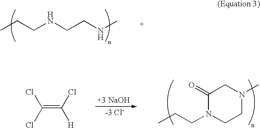
- Similarly, N,N′-dialkylethylenediamine reacts with TCE to yield N,N′-dialkylglycinamide in the presence of a strong base, such as sodium hydroxide according to Equation 4.

- The reactions according to Equations 3 or 4 can provide the basis for detecting TCE by measuring the IR absorbance of the content of the capillary after the reaction at wavelength of 6.03 micrometers.
FIG. 2 correlates the IR absorbance of a sample containing polyglycinamide at wavelength of 6.03 micrometers and the concentration of polyglycinamide in the same sample, which can be stoichiometrically related to the concentration of TCE that reacted. - Detection of Halogenated Hydrocarbons
- Target species may include halogenated hydrocarbons. Halogenated hydrocarbons may include trichloroethane and trihalomethane. The halogenated hydrocarbons may react with pyridine or alkyl-substituted compounds of pyridine to yield colored products in the presence of a strong base according the Fujiwara reaction. A strong base can include sodium hydroxide, potassium hydroxide, or tetrabutylammonium hydroxide (“TBAH”). Colored reaction products of chloroform, bromodichloromethane, chlorodibromomethane, bromoform, and TCE strongly absorb at wavelengths of 538 nm to 540 nm. Thus, an embodiment can be used in conjunction with the Fujiwara reaction to determine heteroatoms and other halogenated hydrocarbons.
- Determination of Polynitroaromatic Compounds
- Polynitroaromatic compounds react with a diamine, such as ethylene diamine, to yield reaction products that exhibit strong absorbance in the visible light spectrum. The reaction can determine the spatial or quantitative distribution of these target species in an area or volume of air. Table 4 shows the wavelengths at the absorbance maxima of selected polynitroaromatic compounds. The wavelength signals identify the corresponding target species.
TABLE 4 Wavelengths of selected polynitroaromatic compound target species. TARGET SPECIES Absorbance Maxima (nm) 1,3,5-trinitrobenzene 455, 540 2,4,6-trinitrobiphenyl 455, 545 2,3′,4,5′,6-pentanitrobiphenyl 450, 555 2,2′,4,4′,6,6′-hexanitrobiphenyl 465, 530 2,4,6-trinitrotoluene 465, 540 2,2′,4,4′,6,6′-hexatrinitrobiphenyl 460, 550 2,2′,4,4′,6,6′-hexanitrostilbene 460, 510 2,2′,4,4′-tetranitrobiphenyl 355, 545 3,3′,5,5′-tetranitrobiphenyl 450, 550 2,2′,6,6′-tetranitrobiphenyl 350, 560 1,4,5,8-tetranitronaphthalene 320, 620 - The spatial and quantitative distribution of polynitrobenzene and selected substituted compounds may be determined. The sensor layer component for each target species obtains a reaction product having absorbance maxima shown in Table 5.
TABLE 5 Reaction product absorbance maxima Absorbance SENSOR Maximum TARGET SPECIES LAYER COMPONENT or Maxima (nm) 1,3-dinitrobenzene Methanolic KOH and acetone 559 1,3,5- dibenzylketone or 2,5- 500 trinitrobenzene pentadione 2-ethoxy-1,3,5- sodium hydroxide and methanol 420, 478, 494 trinitrobenzene 2-methyl-1,3- Strong base and acetone 555 dinitrobenzene 2,4-dimethyl-1,3- Strong base and acetone 651 dinitrobenzene
Detection of Substituted Aromatic - The spatial and quantitative distribution may be determined of selected substituted benzene compounds using the piperonal chloride as the sensor layer component in the presence of a strong acid to obtain a reaction product having absorbance maxima shown in Table 6 according to the following reaction.

TABLE 6 Various moieties on target species and associated absorbance maxima. TARGET SPECIES Absorbance Maximum (nm) CH3 513 OCH3 527 C6H5 560 SCH3 575 SC6H5 585
Detection of Aromatic Aldehydes - A spatial and quantitative distribution may be determined of selected aromatic aldehydes using 2-nitrophenylhydrazine as the sensor layer component in a mixture of 98% (by volume) of dimethylformamide and 2% (by volume) of a 10% (by volume) aqueous solution of tetraethylammonium hydroxide to obtain a reaction product having absorbance maximum shown in Table 7.
TABLE 7 Various target species and associated absorbance maxima. TARGET SPECIES Absorbance Maximum (nm) Benzaldehyde 575 1-napthaldehyde 600 9-anthraldehyde 630 4-dimethylaminocinnamaldehyde 435 2-nitrobenzaldehyde 650 4-nitrobenzaldehyde 665 - Although the exemplary target species disclosed above are organic compounds, appropriate sensor layer components may be used to identify and/or quantify inorganic compounds or inorganic/organic complexes.
- Reference is made to substances, components, or ingredients in existence at the time just before first contacted, formed in situ, blended, or mixed with one or more other substances, components, or ingredients in accordance with the present disclosure. As used herein, interaction refers to a chemical interaction that forms a non-covalently bound species modifying the electronic nature of the interacting intermediates. That is, an interaction refers to two or more chemical compositions in equilibrium. A substance, component or ingredient identified as a reaction product, resulting mixture, or the like may gain an identity, property, or character through a chemical reaction or transformation during the course of contact. That is, a reaction product may form a distinct chemical identity separate from the initial reactants, and that new identity may be based on, for example, covalent bonding. In the range of permanency between an electronic interaction and a chemical reaction, there exists a plurality of states: ionic bonding, complexing, and ligand formation, for example. For purposes of this disclosure, it is necessary to classify these intermediate states as. reaction products unless context or language indicates otherwise. Hence, interaction includes electronic interactions such as the equilibrium adsorption of gas phase molecules onto a surface, and reaction includes a relatively more longer-lasting chemical relationship.
- The transformation of chemical reactants or starting materials to chemical products or final materials is a continually evolving process, independent of the speed at which it occurs. Accordingly, as such a transformative process is in progress there may be a mix of starting and final materials, as well as intermediate species that may be, depending on their kinetic lifetime, easy or difficult to detect with current analytical techniques known to those of ordinary skill in the art.
- Reactants and components referred to by chemical name or formula in the specification or claims hereof, whether referred to in the singular or plural, may be identified as they exist prior to coming into contact with another substance referred to by chemical name or chemical type (e.g., another reactant, target species, or a solvent). Other subsequent changes, transformations, or reactions may result from bringing the specified reactants and/or components together under the conditions called for pursuant to this disclosure. In these other subsequent changes, transformations, or reactions the reactants, ingredients, or the components to be brought together may identify or indicate the reaction product or final material.
- The embodiments described herein are examples of compositions, structures, systems and methods having elements corresponding to the elements of the invention recited in the claims. This written description may enable those of ordinary skill in the art to make and use embodiments having alternative elements that likewise correspond to the elements of the invention recited in the claims. The scope of the invention thus includes compositions, structures, systems and methods that do not differ from the literal language of the claims, and further includes other structures, systems and methods with insubstantial differences from the literal language of the claims. While only certain features and embodiments have been illustrated and described herein, many modifications and changes may occur to one of ordinary skill in the relevant art. The appended claims cover all such modifications and changes.
Claims (30)
Priority Applications (1)
| Application Number | Priority Date | Filing Date | Title |
|---|---|---|---|
| US11/391,744 US20060198760A1 (en) | 2001-08-02 | 2006-03-29 | Opto-acoustic sensor device and associated method |
Applications Claiming Priority (2)
| Application Number | Priority Date | Filing Date | Title |
|---|---|---|---|
| US09/920,281 US20030053936A1 (en) | 2001-08-02 | 2001-08-02 | Opto-acoustic wave chemical sensor |
| US11/391,744 US20060198760A1 (en) | 2001-08-02 | 2006-03-29 | Opto-acoustic sensor device and associated method |
Related Parent Applications (1)
| Application Number | Title | Priority Date | Filing Date |
|---|---|---|---|
| US09/920,281 Continuation-In-Part US20030053936A1 (en) | 1999-11-17 | 2001-08-02 | Opto-acoustic wave chemical sensor |
Publications (1)
| Publication Number | Publication Date |
|---|---|
| US20060198760A1 true US20060198760A1 (en) | 2006-09-07 |
Family
ID=46324177
Family Applications (1)
| Application Number | Title | Priority Date | Filing Date |
|---|---|---|---|
| US11/391,744 Abandoned US20060198760A1 (en) | 2001-08-02 | 2006-03-29 | Opto-acoustic sensor device and associated method |
Country Status (1)
| Country | Link |
|---|---|
| US (1) | US20060198760A1 (en) |
Cited By (25)
| Publication number | Priority date | Publication date | Assignee | Title |
|---|---|---|---|---|
| US20090262298A1 (en) * | 2008-04-18 | 2009-10-22 | Hon Hai Precision Industry Co., Ltd. | Liquid crystal lens and lens module incorporating same |
| US20090268152A1 (en) * | 2008-04-25 | 2009-10-29 | Hon Hai Precision Industry Co., Ltd. | Liquid crystal lens and lens module having same |
| US20100018310A1 (en) * | 2006-05-10 | 2010-01-28 | Drexel University | Molecular control of surface coverage |
| WO2010022158A2 (en) * | 2008-08-19 | 2010-02-25 | The Johns Hopkins University | Piezoelectric polymer fibers |
| US20100277738A1 (en) * | 2009-04-30 | 2010-11-04 | Ta-Jen Yen | Visualized plasmon resonance biodetector |
| US20110038625A1 (en) * | 2009-08-13 | 2011-02-17 | Strategic Polymer Sciences, Inc. | Electromechanical polymer actuators |
| US20110085172A1 (en) * | 2009-04-30 | 2011-04-14 | Ta-Jen Yen | Visualized plasmon resonance biodetector |
| US20110138916A1 (en) * | 2006-01-23 | 2011-06-16 | Drexel University | Self-exciting, self-sensing piezoelectric cantilever sensor |
| US20110143448A1 (en) * | 2009-12-11 | 2011-06-16 | Honeywell Romania S.R.L. | So2 detection using differential nano-resonators and methods related thereto |
| WO2012125649A2 (en) * | 2011-03-14 | 2012-09-20 | Lawrence Livermore National Security, Llc | Non-contact optical system for detecting ultrasound waves from a surface |
| WO2014039271A1 (en) * | 2012-09-04 | 2014-03-13 | Veeco Instruments, Inc. | Apparatus and method for improved acoustical transformation |
| TWI490591B (en) * | 2014-04-11 | 2015-07-01 | Silicon Touch Tech Inc | Liquid crystal lens |
| CN105190301A (en) * | 2012-11-09 | 2015-12-23 | 吉森加斯特斯·李比希大学 | Optical ph value sensor |
| US9362481B2 (en) | 2012-03-05 | 2016-06-07 | The Johns Hopkins University | Continuous piezoelectric film including polar polymer fibers |
| US9538657B2 (en) | 2012-06-29 | 2017-01-03 | General Electric Company | Resonant sensor and an associated sensing method |
| US9536122B2 (en) | 2014-11-04 | 2017-01-03 | General Electric Company | Disposable multivariable sensing devices having radio frequency based sensors |
| US9589686B2 (en) | 2006-11-16 | 2017-03-07 | General Electric Company | Apparatus for detecting contaminants in a liquid and a system for use thereof |
| US9638653B2 (en) | 2010-11-09 | 2017-05-02 | General Electricity Company | Highly selective chemical and biological sensors |
| US9658178B2 (en) | 2012-09-28 | 2017-05-23 | General Electric Company | Sensor systems for measuring an interface level in a multi-phase fluid composition |
| US9746452B2 (en) | 2012-08-22 | 2017-08-29 | General Electric Company | Wireless system and method for measuring an operative condition of a machine |
| CN110186972A (en) * | 2019-05-10 | 2019-08-30 | 济南大学 | A kind of renewable Acetamiprid electrochemical sensor and its preparation method and application |
| WO2019217507A1 (en) * | 2018-05-11 | 2019-11-14 | Carrier Corporation | Photoacoustic detection system |
| US10598650B2 (en) | 2012-08-22 | 2020-03-24 | General Electric Company | System and method for measuring an operative condition of a machine |
| US10684268B2 (en) | 2012-09-28 | 2020-06-16 | Bl Technologies, Inc. | Sensor systems for measuring an interface level in a multi-phase fluid composition |
| US10914698B2 (en) | 2006-11-16 | 2021-02-09 | General Electric Company | Sensing method and system |
Citations (24)
| Publication number | Priority date | Publication date | Assignee | Title |
|---|---|---|---|---|
| US4897541A (en) * | 1984-05-18 | 1990-01-30 | Luxtron Corporation | Sensors for detecting electromagnetic parameters utilizing resonating elements |
| US5411709A (en) * | 1991-03-25 | 1995-05-02 | Fuji Xerox Co., Ltd. | Gas detector |
| US5547877A (en) * | 1994-10-25 | 1996-08-20 | Ensys Environmental Products, Inc. | Methods for the rapid detection of toxic halogenated hydrocarbons and kits useful in performing the same |
| US5756279A (en) * | 1992-07-17 | 1998-05-26 | E. I. Du Pont De Nemours And Company | Analyte detection by means of an analyte-responsive polymer |
| US5880552A (en) * | 1997-05-27 | 1999-03-09 | The United States Of America As Represented By The Secretary Of The Navy | Diamond or diamond like carbon coated chemical sensors and a method of making same |
| US6002702A (en) * | 1997-06-21 | 1999-12-14 | Dragerwerk Ag | Radiation source for laser spectroscopy |
| US6016686A (en) * | 1998-03-16 | 2000-01-25 | Lockheed Martin Energy Research Corporation | Micromechanical potentiometric sensors |
| US6029500A (en) * | 1998-05-19 | 2000-02-29 | Advanced Technology Materials, Inc. | Piezoelectric quartz crystal hydrogen sensor, and hydrogen sensing method utilizing same |
| US6079252A (en) * | 1998-05-20 | 2000-06-27 | Advanced Technology Materials, Inc. | Leak detection device, and fluid vessel assembly comprising same |
| US6118124A (en) * | 1996-01-18 | 2000-09-12 | Lockheed Martin Energy Research Corporation | Electromagnetic and nuclear radiation detector using micromechanical sensors |
| US6154578A (en) * | 1997-03-31 | 2000-11-28 | Samsung Electronics Co., Ltd. | Method for motion compensation of a moving image using two dimensional triangle patch wireframe model |
| US6167748B1 (en) * | 1998-08-31 | 2001-01-02 | Lockheed Martin Energy Research Corporation | Capacitively readout multi-element sensor array with common-mode cancellation |
| US6284198B1 (en) * | 1998-09-30 | 2001-09-04 | K&M Environmental Inc. | Self appearing warning sign device and method of manufacture |
| US6296861B1 (en) * | 1999-05-03 | 2001-10-02 | Nicholas V. Perricone | Treatment of skin damage using conjugated linoleic acid and ascorbyl fatty acid esters |
| US6312959B1 (en) * | 1999-03-30 | 2001-11-06 | U.T. Battelle, Llc | Method using photo-induced and thermal bending of MEMS sensors |
| US6360585B1 (en) * | 2000-03-06 | 2002-03-26 | General Electric Company | Method and apparatus for determining chemical properties |
| US6379623B1 (en) * | 1999-07-12 | 2002-04-30 | Robert Mays, Jr. | System for using luminescent piezoelectric to detect biological and/or chemical agents |
| US20030053936A1 (en) * | 2001-08-02 | 2003-03-20 | General Electric Company | Opto-acoustic wave chemical sensor |
| US6537500B1 (en) * | 1998-07-09 | 2003-03-25 | Hte Aktiengesellschaft | Process for the detection of a product in the discharge of a catalytic material of a plurality of catalytic materials |
| US6618712B1 (en) * | 1999-05-28 | 2003-09-09 | Sandia Corporation | Particle analysis using laser ablation mass spectroscopy |
| US6853812B2 (en) * | 2001-05-09 | 2005-02-08 | Robert Mays, Jr. | Polarized-holographic filtering providing improved extinction ratio |
| US6881585B1 (en) * | 2000-03-06 | 2005-04-19 | General Electric Company | Method and apparatus for rapid screening of volatiles |
| US6955787B1 (en) * | 2003-10-11 | 2005-10-18 | William Paynter Hanson | Integrated biological and chemical sensors |
| US6977506B2 (en) * | 2002-09-18 | 2005-12-20 | National Institute Of Advanced Industrial Science And Technology | Method of analyzing gas using quartz oscillator and apparatus therefor |
-
2006
- 2006-03-29 US US11/391,744 patent/US20060198760A1/en not_active Abandoned
Patent Citations (25)
| Publication number | Priority date | Publication date | Assignee | Title |
|---|---|---|---|---|
| US4897541A (en) * | 1984-05-18 | 1990-01-30 | Luxtron Corporation | Sensors for detecting electromagnetic parameters utilizing resonating elements |
| US5411709A (en) * | 1991-03-25 | 1995-05-02 | Fuji Xerox Co., Ltd. | Gas detector |
| US5756279A (en) * | 1992-07-17 | 1998-05-26 | E. I. Du Pont De Nemours And Company | Analyte detection by means of an analyte-responsive polymer |
| US5547877A (en) * | 1994-10-25 | 1996-08-20 | Ensys Environmental Products, Inc. | Methods for the rapid detection of toxic halogenated hydrocarbons and kits useful in performing the same |
| US6118124A (en) * | 1996-01-18 | 2000-09-12 | Lockheed Martin Energy Research Corporation | Electromagnetic and nuclear radiation detector using micromechanical sensors |
| US6154578A (en) * | 1997-03-31 | 2000-11-28 | Samsung Electronics Co., Ltd. | Method for motion compensation of a moving image using two dimensional triangle patch wireframe model |
| US5880552A (en) * | 1997-05-27 | 1999-03-09 | The United States Of America As Represented By The Secretary Of The Navy | Diamond or diamond like carbon coated chemical sensors and a method of making same |
| US6002702A (en) * | 1997-06-21 | 1999-12-14 | Dragerwerk Ag | Radiation source for laser spectroscopy |
| US6016686A (en) * | 1998-03-16 | 2000-01-25 | Lockheed Martin Energy Research Corporation | Micromechanical potentiometric sensors |
| US6029500A (en) * | 1998-05-19 | 2000-02-29 | Advanced Technology Materials, Inc. | Piezoelectric quartz crystal hydrogen sensor, and hydrogen sensing method utilizing same |
| US6079252A (en) * | 1998-05-20 | 2000-06-27 | Advanced Technology Materials, Inc. | Leak detection device, and fluid vessel assembly comprising same |
| US6537500B1 (en) * | 1998-07-09 | 2003-03-25 | Hte Aktiengesellschaft | Process for the detection of a product in the discharge of a catalytic material of a plurality of catalytic materials |
| US6167748B1 (en) * | 1998-08-31 | 2001-01-02 | Lockheed Martin Energy Research Corporation | Capacitively readout multi-element sensor array with common-mode cancellation |
| US6284198B1 (en) * | 1998-09-30 | 2001-09-04 | K&M Environmental Inc. | Self appearing warning sign device and method of manufacture |
| US6312959B1 (en) * | 1999-03-30 | 2001-11-06 | U.T. Battelle, Llc | Method using photo-induced and thermal bending of MEMS sensors |
| US6296861B1 (en) * | 1999-05-03 | 2001-10-02 | Nicholas V. Perricone | Treatment of skin damage using conjugated linoleic acid and ascorbyl fatty acid esters |
| US6618712B1 (en) * | 1999-05-28 | 2003-09-09 | Sandia Corporation | Particle analysis using laser ablation mass spectroscopy |
| US6379623B1 (en) * | 1999-07-12 | 2002-04-30 | Robert Mays, Jr. | System for using luminescent piezoelectric to detect biological and/or chemical agents |
| US6713307B2 (en) * | 1999-07-12 | 2004-03-30 | R&Dm Foundation | System and method of using luminescent piezoelectric to detect biological and/or chemical agents |
| US6360585B1 (en) * | 2000-03-06 | 2002-03-26 | General Electric Company | Method and apparatus for determining chemical properties |
| US6881585B1 (en) * | 2000-03-06 | 2005-04-19 | General Electric Company | Method and apparatus for rapid screening of volatiles |
| US6853812B2 (en) * | 2001-05-09 | 2005-02-08 | Robert Mays, Jr. | Polarized-holographic filtering providing improved extinction ratio |
| US20030053936A1 (en) * | 2001-08-02 | 2003-03-20 | General Electric Company | Opto-acoustic wave chemical sensor |
| US6977506B2 (en) * | 2002-09-18 | 2005-12-20 | National Institute Of Advanced Industrial Science And Technology | Method of analyzing gas using quartz oscillator and apparatus therefor |
| US6955787B1 (en) * | 2003-10-11 | 2005-10-18 | William Paynter Hanson | Integrated biological and chemical sensors |
Cited By (40)
| Publication number | Priority date | Publication date | Assignee | Title |
|---|---|---|---|---|
| US8511163B2 (en) * | 2006-01-23 | 2013-08-20 | Drexel University | Self-exciting, self-sensing piezoelectric cantilever sensor |
| US20110138916A1 (en) * | 2006-01-23 | 2011-06-16 | Drexel University | Self-exciting, self-sensing piezoelectric cantilever sensor |
| US20100018310A1 (en) * | 2006-05-10 | 2010-01-28 | Drexel University | Molecular control of surface coverage |
| US8286486B2 (en) * | 2006-05-10 | 2012-10-16 | Drexel University | Molecular control of surface coverage |
| US9589686B2 (en) | 2006-11-16 | 2017-03-07 | General Electric Company | Apparatus for detecting contaminants in a liquid and a system for use thereof |
| US10914698B2 (en) | 2006-11-16 | 2021-02-09 | General Electric Company | Sensing method and system |
| US7944543B2 (en) * | 2008-04-18 | 2011-05-17 | Hon Hai Precision Industry Co., Ltd. | Liquid crystal lens and lens module incorporating same |
| US20090262298A1 (en) * | 2008-04-18 | 2009-10-22 | Hon Hai Precision Industry Co., Ltd. | Liquid crystal lens and lens module incorporating same |
| US7880858B2 (en) * | 2008-04-25 | 2011-02-01 | Hon Hai Precision Industry Co., Ltd. | Liquid crystal lens and lens module having same |
| US20090268152A1 (en) * | 2008-04-25 | 2009-10-29 | Hon Hai Precision Industry Co., Ltd. | Liquid crystal lens and lens module having same |
| WO2010022158A2 (en) * | 2008-08-19 | 2010-02-25 | The Johns Hopkins University | Piezoelectric polymer fibers |
| US20110260584A1 (en) * | 2008-08-19 | 2011-10-27 | Michael Yu | Piezoelectric polymer fibers |
| WO2010022158A3 (en) * | 2008-08-19 | 2010-05-14 | The Johns Hopkins University | Piezoelectric polymer fibers |
| US8946974B2 (en) * | 2008-08-19 | 2015-02-03 | The Johns Hopkins University | Piezoelectric polymer fibers |
| US20110085172A1 (en) * | 2009-04-30 | 2011-04-14 | Ta-Jen Yen | Visualized plasmon resonance biodetector |
| US20100277738A1 (en) * | 2009-04-30 | 2010-11-04 | Ta-Jen Yen | Visualized plasmon resonance biodetector |
| US20110038625A1 (en) * | 2009-08-13 | 2011-02-17 | Strategic Polymer Sciences, Inc. | Electromechanical polymer actuators |
| US20110143448A1 (en) * | 2009-12-11 | 2011-06-16 | Honeywell Romania S.R.L. | So2 detection using differential nano-resonators and methods related thereto |
| US8609427B2 (en) * | 2009-12-11 | 2013-12-17 | Honeywell Romania S.R.L. | SO2 detection using differential nano-resonators and methods related thereto |
| US9638653B2 (en) | 2010-11-09 | 2017-05-02 | General Electricity Company | Highly selective chemical and biological sensors |
| WO2012125649A2 (en) * | 2011-03-14 | 2012-09-20 | Lawrence Livermore National Security, Llc | Non-contact optical system for detecting ultrasound waves from a surface |
| US10390709B2 (en) | 2011-03-14 | 2019-08-27 | Lawrence Livermore National Security, Llc | Non-contact optical system for detecting ultrasound waves from a surface |
| WO2012125649A3 (en) * | 2011-03-14 | 2012-12-06 | Lawrence Livermore National Security, Llc | Non-contact optical system for detecting ultrasound waves from a surface |
| US9362481B2 (en) | 2012-03-05 | 2016-06-07 | The Johns Hopkins University | Continuous piezoelectric film including polar polymer fibers |
| US9538657B2 (en) | 2012-06-29 | 2017-01-03 | General Electric Company | Resonant sensor and an associated sensing method |
| US10598650B2 (en) | 2012-08-22 | 2020-03-24 | General Electric Company | System and method for measuring an operative condition of a machine |
| US9746452B2 (en) | 2012-08-22 | 2017-08-29 | General Electric Company | Wireless system and method for measuring an operative condition of a machine |
| US9804126B2 (en) | 2012-09-04 | 2017-10-31 | Veeco Instruments Inc. | Apparatus and method for improved acoustical transformation |
| CN104781661A (en) * | 2012-09-04 | 2015-07-15 | 维易科仪器有限公司 | Apparatus and method for improved acoustical transformation |
| WO2014039271A1 (en) * | 2012-09-04 | 2014-03-13 | Veeco Instruments, Inc. | Apparatus and method for improved acoustical transformation |
| US9658178B2 (en) | 2012-09-28 | 2017-05-23 | General Electric Company | Sensor systems for measuring an interface level in a multi-phase fluid composition |
| US10684268B2 (en) | 2012-09-28 | 2020-06-16 | Bl Technologies, Inc. | Sensor systems for measuring an interface level in a multi-phase fluid composition |
| CN105190301A (en) * | 2012-11-09 | 2015-12-23 | 吉森加斯特斯·李比希大学 | Optical ph value sensor |
| US9897804B2 (en) | 2014-04-11 | 2018-02-20 | Silicon Touch Technology Inc. | Liquid crystal lens |
| TWI490591B (en) * | 2014-04-11 | 2015-07-01 | Silicon Touch Tech Inc | Liquid crystal lens |
| US9536122B2 (en) | 2014-11-04 | 2017-01-03 | General Electric Company | Disposable multivariable sensing devices having radio frequency based sensors |
| WO2019217507A1 (en) * | 2018-05-11 | 2019-11-14 | Carrier Corporation | Photoacoustic detection system |
| CN112384785A (en) * | 2018-05-11 | 2021-02-19 | 开利公司 | Photoacoustic detection system |
| US11754533B2 (en) | 2018-05-11 | 2023-09-12 | Carrier Corporation | Photoacoustic detection system with clocked tuning fork positions |
| CN110186972A (en) * | 2019-05-10 | 2019-08-30 | 济南大学 | A kind of renewable Acetamiprid electrochemical sensor and its preparation method and application |
Similar Documents
| Publication | Publication Date | Title |
|---|---|---|
| US20060198760A1 (en) | Opto-acoustic sensor device and associated method | |
| US20060210440A1 (en) | Opto-acoustic sensor system and associated method | |
| Mehrvar et al. | Fiber-optic biosensors-trends and advances | |
| Wolfbeis | Fiber-optic chemical sensors and biosensors | |
| US5866430A (en) | Raman optrode processes and devices for detection of chemicals and microorganisms | |
| King et al. | Detecting staphylococcal enterotoxin B using an automated fiber optic biosensor | |
| US6040191A (en) | Raman spectroscopic method for determining the ligand binding capacity of biologicals | |
| Viveros et al. | A fluorescence-based biosensor for the detection of organophosphate pesticides and chemical warfare agents | |
| US7429357B2 (en) | Apparatus, system, and method of detecting an analyte utilizing pyroelectric technology | |
| KR100878093B1 (en) | A biological measurement system and a method of detecting a pathogen using the same | |
| US20030053936A1 (en) | Opto-acoustic wave chemical sensor | |
| WO2000029820A2 (en) | Probe for evanescent excitation of fluorescence | |
| Narayanaswamy et al. | Optical fibre sensors for chemical species | |
| US20120164027A1 (en) | Polymer Based Lanthanide Luminescent Sensors for the Detection of Organophosphorus Compounds | |
| Stavra et al. | Fast, sensitive and selective determination of herbicide glyphosate in water samples with a White Light Reflectance Spectroscopy immunosensor | |
| JP2005140794A (en) | Raman opto load process and device for detecting chemical substance and microorganism | |
| Lau et al. | Quantitative colorimetric analysis of dye mixtures using an optical photometer based on LED array | |
| US6521185B1 (en) | Fluorescent probes based on the affinity of a polymer matrix for an analyte of interest | |
| US10324034B2 (en) | Self-referencing localized plasmon resonance sensing device and system thereof | |
| CN101294900B (en) | High-fineness cavity surface plasma resonance sensing equipment | |
| Yu et al. | An optical fiber sensor probe using a PMMA/CPR coated bent optical fiber as a transducer for monitoring trace ammonia | |
| Anderson et al. | Raptor: A portable, automated biosensor | |
| US20180080902A1 (en) | Use of piezoelectric transducers modified with metal oxide-based thin films for direct detection of amine derivatives in liquid media | |
| WO2000014515A9 (en) | Low frequency modulation sensors using nanosecond fluorophores | |
| Wang et al. | Sensitive detection of TNT using competition assay on quartz crystal microbalance |
Legal Events
| Date | Code | Title | Description |
|---|---|---|---|
| AS | Assignment |
Owner name: GENERAL ELECTRIC COMPANY, NEW YORK Free format text: ASSIGNMENT OF ASSIGNORS INTEREST;ASSIGNORS:POTYRAILO, RADISLAV ALEXANDROVICH;SIVAVEC, TIMOTHY MARK;SALVO, JOSEPH JAMES;REEL/FRAME:017864/0811;SIGNING DATES FROM 20060331 TO 20060403 |
|
| AS | Assignment |
Owner name: SABIC INNOVATIVE PLASTICS IP B.V., NETHERLANDS Free format text: ASSIGNMENT OF ASSIGNORS INTEREST;ASSIGNOR:GENERAL ELECTRIC COMPANY;REEL/FRAME:020985/0551 Effective date: 20070831 Owner name: SABIC INNOVATIVE PLASTICS IP B.V.,NETHERLANDS Free format text: ASSIGNMENT OF ASSIGNORS INTEREST;ASSIGNOR:GENERAL ELECTRIC COMPANY;REEL/FRAME:020985/0551 Effective date: 20070831 |
|
| AS | Assignment |
Owner name: CITIBANK, N.A., AS COLLATERAL AGENT, NEW YORK Free format text: SECURITY AGREEMENT;ASSIGNOR:SABIC INNOVATIVE PLASTICS IP B.V.;REEL/FRAME:021423/0001 Effective date: 20080307 Owner name: CITIBANK, N.A., AS COLLATERAL AGENT,NEW YORK Free format text: SECURITY AGREEMENT;ASSIGNOR:SABIC INNOVATIVE PLASTICS IP B.V.;REEL/FRAME:021423/0001 Effective date: 20080307 |
|
| STCB | Information on status: application discontinuation |
Free format text: ABANDONED -- FAILURE TO RESPOND TO AN OFFICE ACTION |