EP3236501A1 - Back-illuminated sensor with boron layer - Google Patents
Back-illuminated sensor with boron layer Download PDFInfo
- Publication number
- EP3236501A1 EP3236501A1 EP17172675.5A EP17172675A EP3236501A1 EP 3236501 A1 EP3236501 A1 EP 3236501A1 EP 17172675 A EP17172675 A EP 17172675A EP 3236501 A1 EP3236501 A1 EP 3236501A1
- Authority
- EP
- European Patent Office
- Prior art keywords
- sensor
- image sensor
- inspection system
- layer
- image
- Prior art date
- Legal status (The legal status is an assumption and is not a legal conclusion. Google has not performed a legal analysis and makes no representation as to the accuracy of the status listed.)
- Granted
Links
- 229910052796 boron Inorganic materials 0.000 title claims abstract description 78
- ZOXJGFHDIHLPTG-UHFFFAOYSA-N Boron Chemical compound [B] ZOXJGFHDIHLPTG-UHFFFAOYSA-N 0.000 title claims abstract description 76
- 239000004065 semiconductor Substances 0.000 claims abstract description 51
- 238000007689 inspection Methods 0.000 claims abstract description 50
- 239000012528 membrane Substances 0.000 claims abstract description 34
- 229910052710 silicon Inorganic materials 0.000 claims description 27
- 239000010703 silicon Substances 0.000 claims description 27
- 238000005286 illumination Methods 0.000 claims description 26
- XUIMIQQOPSSXEZ-UHFFFAOYSA-N Silicon Chemical compound [Si] XUIMIQQOPSSXEZ-UHFFFAOYSA-N 0.000 claims description 24
- 238000000576 coating method Methods 0.000 claims description 24
- 239000011248 coating agent Substances 0.000 claims description 22
- 238000012545 processing Methods 0.000 claims description 14
- 239000003870 refractory metal Substances 0.000 claims description 11
- 238000006243 chemical reaction Methods 0.000 claims description 4
- 239000002245 particle Substances 0.000 abstract description 23
- 238000005516 engineering process Methods 0.000 abstract description 4
- 230000004907 flux Effects 0.000 abstract description 4
- 230000000295 complement effect Effects 0.000 abstract description 2
- 229910044991 metal oxide Inorganic materials 0.000 abstract description 2
- 150000004706 metal oxides Chemical class 0.000 abstract description 2
- 239000010410 layer Substances 0.000 description 165
- 235000012431 wafers Nutrition 0.000 description 58
- 239000000758 substrate Substances 0.000 description 48
- VYPSYNLAJGMNEJ-UHFFFAOYSA-N Silicium dioxide Chemical compound O=[Si]=O VYPSYNLAJGMNEJ-UHFFFAOYSA-N 0.000 description 43
- 238000000034 method Methods 0.000 description 39
- 235000012239 silicon dioxide Nutrition 0.000 description 22
- 239000000377 silicon dioxide Substances 0.000 description 19
- 239000000463 material Substances 0.000 description 18
- 229910052751 metal Inorganic materials 0.000 description 17
- 239000002184 metal Substances 0.000 description 17
- 238000000151 deposition Methods 0.000 description 16
- 230000005855 radiation Effects 0.000 description 16
- 230000008021 deposition Effects 0.000 description 13
- 239000011241 protective layer Substances 0.000 description 13
- 238000004140 cleaning Methods 0.000 description 11
- 230000007547 defect Effects 0.000 description 8
- 238000004519 manufacturing process Methods 0.000 description 8
- 230000035945 sensitivity Effects 0.000 description 8
- 230000005540 biological transmission Effects 0.000 description 7
- 230000008569 process Effects 0.000 description 7
- 229910052581 Si3N4 Inorganic materials 0.000 description 6
- 238000005530 etching Methods 0.000 description 6
- HQVNEWCFYHHQES-UHFFFAOYSA-N silicon nitride Chemical compound N12[Si]34N5[Si]62N3[Si]51N64 HQVNEWCFYHHQES-UHFFFAOYSA-N 0.000 description 6
- 238000010521 absorption reaction Methods 0.000 description 5
- 125000004429 atom Chemical group 0.000 description 5
- 239000004020 conductor Substances 0.000 description 5
- 239000002019 doping agent Substances 0.000 description 5
- 238000003384 imaging method Methods 0.000 description 5
- 238000001459 lithography Methods 0.000 description 5
- UFHFLCQGNIYNRP-UHFFFAOYSA-N Hydrogen Chemical compound [H][H] UFHFLCQGNIYNRP-UHFFFAOYSA-N 0.000 description 4
- 230000008901 benefit Effects 0.000 description 4
- 229910052799 carbon Inorganic materials 0.000 description 4
- 239000000356 contaminant Substances 0.000 description 4
- 239000001257 hydrogen Substances 0.000 description 4
- 229910052739 hydrogen Inorganic materials 0.000 description 4
- 238000005468 ion implantation Methods 0.000 description 4
- PQXKHYXIUOZZFA-UHFFFAOYSA-M lithium fluoride Chemical compound [Li+].[F-] PQXKHYXIUOZZFA-UHFFFAOYSA-M 0.000 description 4
- 230000033001 locomotion Effects 0.000 description 4
- 150000002739 metals Chemical class 0.000 description 4
- 230000003287 optical effect Effects 0.000 description 4
- 229910021420 polycrystalline silicon Inorganic materials 0.000 description 4
- 238000005036 potential barrier Methods 0.000 description 4
- 238000002360 preparation method Methods 0.000 description 4
- 230000001681 protective effect Effects 0.000 description 4
- 238000012546 transfer Methods 0.000 description 4
- OKTJSMMVPCPJKN-UHFFFAOYSA-N Carbon Chemical compound [C] OKTJSMMVPCPJKN-UHFFFAOYSA-N 0.000 description 3
- 238000000137 annealing Methods 0.000 description 3
- 230000015556 catabolic process Effects 0.000 description 3
- 238000006731 degradation reaction Methods 0.000 description 3
- 239000003989 dielectric material Substances 0.000 description 3
- 238000001035 drying Methods 0.000 description 3
- 239000007789 gas Substances 0.000 description 3
- 230000010354 integration Effects 0.000 description 3
- 229910001635 magnesium fluoride Inorganic materials 0.000 description 3
- 239000000203 mixture Substances 0.000 description 3
- 238000005498 polishing Methods 0.000 description 3
- 239000010453 quartz Substances 0.000 description 3
- IJGRMHOSHXDMSA-UHFFFAOYSA-N Atomic nitrogen Chemical compound N#N IJGRMHOSHXDMSA-UHFFFAOYSA-N 0.000 description 2
- 230000003321 amplification Effects 0.000 description 2
- 230000015572 biosynthetic process Effects 0.000 description 2
- 239000003990 capacitor Substances 0.000 description 2
- 238000001444 catalytic combustion detection Methods 0.000 description 2
- 239000000919 ceramic Substances 0.000 description 2
- 238000011109 contamination Methods 0.000 description 2
- 238000001514 detection method Methods 0.000 description 2
- 230000005684 electric field Effects 0.000 description 2
- 239000012212 insulator Substances 0.000 description 2
- 150000002500 ions Chemical class 0.000 description 2
- ORUIBWPALBXDOA-UHFFFAOYSA-L magnesium fluoride Chemical compound [F-].[F-].[Mg+2] ORUIBWPALBXDOA-UHFFFAOYSA-L 0.000 description 2
- 238000003199 nucleic acid amplification method Methods 0.000 description 2
- 238000000059 patterning Methods 0.000 description 2
- 238000002310 reflectometry Methods 0.000 description 2
- 229910052594 sapphire Inorganic materials 0.000 description 2
- 239000010980 sapphire Substances 0.000 description 2
- 229910000679 solder Inorganic materials 0.000 description 2
- 239000007787 solid Substances 0.000 description 2
- XLYOFNOQVPJJNP-UHFFFAOYSA-N water Substances O XLYOFNOQVPJJNP-UHFFFAOYSA-N 0.000 description 2
- VYZAMTAEIAYCRO-UHFFFAOYSA-N Chromium Chemical compound [Cr] VYZAMTAEIAYCRO-UHFFFAOYSA-N 0.000 description 1
- 241000197727 Euscorpius alpha Species 0.000 description 1
- 229910002601 GaN Inorganic materials 0.000 description 1
- 229910001218 Gallium arsenide Inorganic materials 0.000 description 1
- YZCKVEUIGOORGS-UHFFFAOYSA-N Hydrogen atom Chemical compound [H] YZCKVEUIGOORGS-UHFFFAOYSA-N 0.000 description 1
- KJTLSVCANCCWHF-UHFFFAOYSA-N Ruthenium Chemical compound [Ru] KJTLSVCANCCWHF-UHFFFAOYSA-N 0.000 description 1
- RTAQQCXQSZGOHL-UHFFFAOYSA-N Titanium Chemical compound [Ti] RTAQQCXQSZGOHL-UHFFFAOYSA-N 0.000 description 1
- 241000724291 Tobacco streak virus Species 0.000 description 1
- 238000001994 activation Methods 0.000 description 1
- 230000004913 activation Effects 0.000 description 1
- 229910052783 alkali metal Inorganic materials 0.000 description 1
- 150000001340 alkali metals Chemical class 0.000 description 1
- 229910052782 aluminium Inorganic materials 0.000 description 1
- PNEYBMLMFCGWSK-UHFFFAOYSA-N aluminium oxide Inorganic materials [O-2].[O-2].[O-2].[Al+3].[Al+3] PNEYBMLMFCGWSK-UHFFFAOYSA-N 0.000 description 1
- 238000003491 array Methods 0.000 description 1
- 238000000429 assembly Methods 0.000 description 1
- 230000000712 assembly Effects 0.000 description 1
- QVGXLLKOCUKJST-UHFFFAOYSA-N atomic oxygen Chemical compound [O] QVGXLLKOCUKJST-UHFFFAOYSA-N 0.000 description 1
- 229910052792 caesium Inorganic materials 0.000 description 1
- TVFDJXOCXUVLDH-UHFFFAOYSA-N caesium atom Chemical compound [Cs] TVFDJXOCXUVLDH-UHFFFAOYSA-N 0.000 description 1
- 150000001721 carbon Chemical class 0.000 description 1
- -1 cesium Chemical class 0.000 description 1
- 238000003486 chemical etching Methods 0.000 description 1
- 238000005229 chemical vapour deposition Methods 0.000 description 1
- 229910052804 chromium Inorganic materials 0.000 description 1
- 239000011651 chromium Substances 0.000 description 1
- 238000004320 controlled atmosphere Methods 0.000 description 1
- 229910052802 copper Inorganic materials 0.000 description 1
- PMHQVHHXPFUNSP-UHFFFAOYSA-M copper(1+);methylsulfanylmethane;bromide Chemical compound Br[Cu].CSC PMHQVHHXPFUNSP-UHFFFAOYSA-M 0.000 description 1
- 239000013078 crystal Substances 0.000 description 1
- 238000013461 design Methods 0.000 description 1
- 239000003822 epoxy resin Substances 0.000 description 1
- 238000001900 extreme ultraviolet lithography Methods 0.000 description 1
- 239000003574 free electron Substances 0.000 description 1
- 239000005350 fused silica glass Substances 0.000 description 1
- 239000001307 helium Substances 0.000 description 1
- 229910052734 helium Inorganic materials 0.000 description 1
- SWQJXJOGLNCZEY-UHFFFAOYSA-N helium atom Chemical compound [He] SWQJXJOGLNCZEY-UHFFFAOYSA-N 0.000 description 1
- 150000002431 hydrogen Chemical class 0.000 description 1
- 239000012535 impurity Substances 0.000 description 1
- 230000002427 irreversible effect Effects 0.000 description 1
- 230000005012 migration Effects 0.000 description 1
- 238000013508 migration Methods 0.000 description 1
- 229910052757 nitrogen Inorganic materials 0.000 description 1
- 239000012299 nitrogen atmosphere Substances 0.000 description 1
- 230000003647 oxidation Effects 0.000 description 1
- 238000007254 oxidation reaction Methods 0.000 description 1
- 239000001301 oxygen Substances 0.000 description 1
- 229910052760 oxygen Inorganic materials 0.000 description 1
- 238000004806 packaging method and process Methods 0.000 description 1
- 238000012856 packing Methods 0.000 description 1
- 238000002161 passivation Methods 0.000 description 1
- 230000035515 penetration Effects 0.000 description 1
- 230000010363 phase shift Effects 0.000 description 1
- 238000000206 photolithography Methods 0.000 description 1
- 229920002120 photoresistant polymer Polymers 0.000 description 1
- 238000000623 plasma-assisted chemical vapour deposition Methods 0.000 description 1
- 230000010287 polarization Effects 0.000 description 1
- 238000007517 polishing process Methods 0.000 description 1
- 229920000647 polyepoxide Polymers 0.000 description 1
- 238000011084 recovery Methods 0.000 description 1
- 229910052703 rhodium Inorganic materials 0.000 description 1
- 239000010948 rhodium Substances 0.000 description 1
- MHOVAHRLVXNVSD-UHFFFAOYSA-N rhodium atom Chemical compound [Rh] MHOVAHRLVXNVSD-UHFFFAOYSA-N 0.000 description 1
- 229910052707 ruthenium Inorganic materials 0.000 description 1
- 229910021332 silicide Inorganic materials 0.000 description 1
- FVBUAEGBCNSCDD-UHFFFAOYSA-N silicide(4-) Chemical compound [Si-4] FVBUAEGBCNSCDD-UHFFFAOYSA-N 0.000 description 1
- 239000002356 single layer Substances 0.000 description 1
- 238000003892 spreading Methods 0.000 description 1
- 230000007480 spreading Effects 0.000 description 1
- 238000004544 sputter deposition Methods 0.000 description 1
- 238000003860 storage Methods 0.000 description 1
- 239000000126 substance Substances 0.000 description 1
- 238000004381 surface treatment Methods 0.000 description 1
- 230000001360 synchronised effect Effects 0.000 description 1
- 229910052715 tantalum Inorganic materials 0.000 description 1
- GUVRBAGPIYLISA-UHFFFAOYSA-N tantalum atom Chemical compound [Ta] GUVRBAGPIYLISA-UHFFFAOYSA-N 0.000 description 1
- 238000007725 thermal activation Methods 0.000 description 1
- 229910052719 titanium Inorganic materials 0.000 description 1
- 239000010936 titanium Substances 0.000 description 1
- VLCQZHSMCYCDJL-UHFFFAOYSA-N tribenuron methyl Chemical compound COC(=O)C1=CC=CC=C1S(=O)(=O)NC(=O)N(C)C1=NC(C)=NC(OC)=N1 VLCQZHSMCYCDJL-UHFFFAOYSA-N 0.000 description 1
- WFKWXMTUELFFGS-UHFFFAOYSA-N tungsten Chemical compound [W] WFKWXMTUELFFGS-UHFFFAOYSA-N 0.000 description 1
- 229910052721 tungsten Inorganic materials 0.000 description 1
- 239000010937 tungsten Substances 0.000 description 1
- 229910052720 vanadium Inorganic materials 0.000 description 1
- LEONUFNNVUYDNQ-UHFFFAOYSA-N vanadium atom Chemical compound [V] LEONUFNNVUYDNQ-UHFFFAOYSA-N 0.000 description 1
Images


Classifications
-
- H—ELECTRICITY
- H01—ELECTRIC ELEMENTS
- H01L—SEMICONDUCTOR DEVICES NOT COVERED BY CLASS H10
- H01L31/00—Semiconductor devices sensitive to infrared radiation, light, electromagnetic radiation of shorter wavelength or corpuscular radiation and specially adapted either for the conversion of the energy of such radiation into electrical energy or for the control of electrical energy by such radiation; Processes or apparatus specially adapted for the manufacture or treatment thereof or of parts thereof; Details thereof
- H01L31/02—Details
- H01L31/0216—Coatings
-
- G—PHYSICS
- G01—MEASURING; TESTING
- G01N—INVESTIGATING OR ANALYSING MATERIALS BY DETERMINING THEIR CHEMICAL OR PHYSICAL PROPERTIES
- G01N21/00—Investigating or analysing materials by the use of optical means, i.e. using sub-millimetre waves, infrared, visible or ultraviolet light
- G01N21/84—Systems specially adapted for particular applications
- G01N21/88—Investigating the presence of flaws or contamination
- G01N21/8806—Specially adapted optical and illumination features
-
- G—PHYSICS
- G01—MEASURING; TESTING
- G01N—INVESTIGATING OR ANALYSING MATERIALS BY DETERMINING THEIR CHEMICAL OR PHYSICAL PROPERTIES
- G01N21/00—Investigating or analysing materials by the use of optical means, i.e. using sub-millimetre waves, infrared, visible or ultraviolet light
- G01N21/84—Systems specially adapted for particular applications
- G01N21/88—Investigating the presence of flaws or contamination
- G01N21/95—Investigating the presence of flaws or contamination characterised by the material or shape of the object to be examined
- G01N21/9501—Semiconductor wafers
-
- G—PHYSICS
- G01—MEASURING; TESTING
- G01N—INVESTIGATING OR ANALYSING MATERIALS BY DETERMINING THEIR CHEMICAL OR PHYSICAL PROPERTIES
- G01N21/00—Investigating or analysing materials by the use of optical means, i.e. using sub-millimetre waves, infrared, visible or ultraviolet light
- G01N21/84—Systems specially adapted for particular applications
- G01N21/88—Investigating the presence of flaws or contamination
- G01N21/95—Investigating the presence of flaws or contamination characterised by the material or shape of the object to be examined
- G01N21/956—Inspecting patterns on the surface of objects
-
- H—ELECTRICITY
- H01—ELECTRIC ELEMENTS
- H01L—SEMICONDUCTOR DEVICES NOT COVERED BY CLASS H10
- H01L27/00—Devices consisting of a plurality of semiconductor or other solid-state components formed in or on a common substrate
- H01L27/14—Devices consisting of a plurality of semiconductor or other solid-state components formed in or on a common substrate including semiconductor components sensitive to infrared radiation, light, electromagnetic radiation of shorter wavelength or corpuscular radiation and specially adapted either for the conversion of the energy of such radiation into electrical energy or for the control of electrical energy by such radiation
- H01L27/144—Devices controlled by radiation
- H01L27/146—Imager structures
- H01L27/14601—Structural or functional details thereof
- H01L27/1462—Coatings
-
- H—ELECTRICITY
- H01—ELECTRIC ELEMENTS
- H01L—SEMICONDUCTOR DEVICES NOT COVERED BY CLASS H10
- H01L27/00—Devices consisting of a plurality of semiconductor or other solid-state components formed in or on a common substrate
- H01L27/14—Devices consisting of a plurality of semiconductor or other solid-state components formed in or on a common substrate including semiconductor components sensitive to infrared radiation, light, electromagnetic radiation of shorter wavelength or corpuscular radiation and specially adapted either for the conversion of the energy of such radiation into electrical energy or for the control of electrical energy by such radiation
- H01L27/144—Devices controlled by radiation
- H01L27/146—Imager structures
- H01L27/14601—Structural or functional details thereof
- H01L27/1464—Back illuminated imager structures
-
- H—ELECTRICITY
- H01—ELECTRIC ELEMENTS
- H01L—SEMICONDUCTOR DEVICES NOT COVERED BY CLASS H10
- H01L27/00—Devices consisting of a plurality of semiconductor or other solid-state components formed in or on a common substrate
- H01L27/14—Devices consisting of a plurality of semiconductor or other solid-state components formed in or on a common substrate including semiconductor components sensitive to infrared radiation, light, electromagnetic radiation of shorter wavelength or corpuscular radiation and specially adapted either for the conversion of the energy of such radiation into electrical energy or for the control of electrical energy by such radiation
- H01L27/144—Devices controlled by radiation
- H01L27/146—Imager structures
- H01L27/14683—Processes or apparatus peculiar to the manufacture or treatment of these devices or parts thereof
- H01L27/14685—Process for coatings or optical elements
-
- H—ELECTRICITY
- H01—ELECTRIC ELEMENTS
- H01L—SEMICONDUCTOR DEVICES NOT COVERED BY CLASS H10
- H01L27/00—Devices consisting of a plurality of semiconductor or other solid-state components formed in or on a common substrate
- H01L27/14—Devices consisting of a plurality of semiconductor or other solid-state components formed in or on a common substrate including semiconductor components sensitive to infrared radiation, light, electromagnetic radiation of shorter wavelength or corpuscular radiation and specially adapted either for the conversion of the energy of such radiation into electrical energy or for the control of electrical energy by such radiation
- H01L27/144—Devices controlled by radiation
- H01L27/146—Imager structures
- H01L27/148—Charge coupled imagers
- H01L27/14806—Structural or functional details thereof
-
- G—PHYSICS
- G01—MEASURING; TESTING
- G01N—INVESTIGATING OR ANALYSING MATERIALS BY DETERMINING THEIR CHEMICAL OR PHYSICAL PROPERTIES
- G01N21/00—Investigating or analysing materials by the use of optical means, i.e. using sub-millimetre waves, infrared, visible or ultraviolet light
- G01N21/84—Systems specially adapted for particular applications
- G01N21/88—Investigating the presence of flaws or contamination
- G01N21/95—Investigating the presence of flaws or contamination characterised by the material or shape of the object to be examined
- G01N21/956—Inspecting patterns on the surface of objects
- G01N2021/95676—Masks, reticles, shadow masks
-
- H—ELECTRICITY
- H01—ELECTRIC ELEMENTS
- H01L—SEMICONDUCTOR DEVICES NOT COVERED BY CLASS H10
- H01L27/00—Devices consisting of a plurality of semiconductor or other solid-state components formed in or on a common substrate
- H01L27/14—Devices consisting of a plurality of semiconductor or other solid-state components formed in or on a common substrate including semiconductor components sensitive to infrared radiation, light, electromagnetic radiation of shorter wavelength or corpuscular radiation and specially adapted either for the conversion of the energy of such radiation into electrical energy or for the control of electrical energy by such radiation
- H01L27/144—Devices controlled by radiation
- H01L27/146—Imager structures
- H01L27/14683—Processes or apparatus peculiar to the manufacture or treatment of these devices or parts thereof
- H01L27/14689—MOS based technologies
Definitions
- the present application relates to image sensors suitable for sensing radiation in deep UV (DUV), vacuum UV (VUV), and extreme UV (EUV) wavelength, and to methods for making such image sensors.
- Some embodiments of the sensors are suitable for sensing electrons and other charged particles. All of the sensors are suitable for use in photomask, reticle, or wafer inspection systems.
- the integrated circuit industry requires inspection tools with increasingly higher resolution to resolve ever smaller features of integrated circuits, photomasks, reticles, solar cells, charge coupled devices etc., as well as detect defects whose sizes are of the order of, or smaller than, those feature sizes.
- Inspection systems operating at short wavelengths can provide such resolution in many cases.
- electrons or other charged particles such as helium (He) nuclei (i.e. alpha particles) may be used.
- He helium
- inspection systems operating over a relatively broad range of wavelengths, such as a wavelength range that includes wavelengths in the near UV, DUV, and/or VUV ranges, can be advantageous because a broad range of wavelengths can reduce the sensitivity to small changes in layer thicknesses or pattern dimensions that can cause large changes in reflectivity at an individual wavelength.
- a photon with a vacuum wavelength of 250 nm has energy of approximately 5 eV.
- the bandgap of silicon dioxide is about 10 eV.
- silicon dioxide as grown on a silicon surface must have some dangling bonds at the interface with the silicon because the silicon dioxide structure cannot perfectly match that of the silicon crystal.
- the single dioxide is amorphous, there are likely also some dangling bonds within the material.
- two high-energy photons may arrive near the same location within a very short time interval (nanoseconds or picoseconds), which can lead to electrons being excited to the conduction band of the silicon dioxide by two absorption events in rapid succession or by two-photon absorption.
- EUV photons have very high energies (13.5 nm in wavelength corresponds to photon energy close to 92 eV) and are capable of breaking silicon-oxygen bonds as well as strongly interacting with defects and contaminants in the oxide.
- Electron and charged-particle detectors typically have to detect electrons or charged particles with energies of a few hundred eV or higher. Energys greater than 10 eV can readily break silicon-oxygen bonds.
- High-energy particles and photons can also cause irreversible changes to the silicon dioxide. Such changes can include reconfiguration of the bonding of atoms or migration of small atoms within the silicon dioxide. At normal operating temperatures of the detector, which are typically in a range from around room temperature to about 50°C, these changes will not recover. In particular, it is known that conventional silicon photodiodes used as EUV detectors degrade in efficiency with use.
- the silicon dioxide layer on the surface of semiconductor detectors significantly reduces the efficiency of those detectors for low-energy (less than about 2 kV) electrons. Some low-energy electrons are absorbed by the silicon dioxide, thereby causing the silicon dioxide to charge up and deflect subsequent arriving electrons. Because a native oxide will always form on an exposed silicon surface, silicon detectors necessarily must have some oxide on their surface. Growing or depositing an alternative dielectric material (instead of the oxide) on the surface of the semiconductor results in a much higher density of defect states at the semiconductor to silicon dioxide interface. These defects reduce the quantum efficiency of the detector, especially for photons or charged particles absorbed close to the surface of the semiconductor.
- An additional cause of degradation of EUV sensors is that, in a EUV system, a thin layer of carbon builds up over time on any surface exposed to EUV radiation, including the surface of the image sensors and optical elements. This carbon layer, as it becomes thicker, absorbs EUV radiation and reduces the sensitivity of the sensor, as well as reducing the reflectivity of optical elements in the light path.
- all surfaces exposed to EUV are periodically cleaned to remove the carbon. This cleaning is usually performed with activated hydrogen (a mixture of atomic hydrogen and hydrogen radicals), which is very effective at removing carbon.
- activated hydrogen a mixture of atomic hydrogen and hydrogen radicals
- hydrogen radicals affect the oxide on the surface of silicon detectors and can also cause degradation of the performance of those sensors.
- Diode detectors suitable for detecting EUV and/or electrons are known in the art. Exemplary diode detectors are described in US Patent 8,138,485 issued to Nihtianov on March 20, 2012 , US Patent 7,586,108 issued to Nihtianov on September 8, 2009 , US Published Application 2012/0268722 published on October 25, 2012 (filed by Nihtianov ), and US Published Application 2011/0169116 published on July 14, 2011 (filed by Nanver ), These diode detectors include a thin (1nm to 20nm) layer of boron directly on the silicon surface. US Published Application 2011/0169116 further describes an open mesh of a metallic conductor on the surface of such a detector.
- detectors have contacts formed on the top (light or electron-incident) surface.
- a disadvantage of having contacts and conductors formed on the illuminated surface is that it is not possible to create a detector with a large number (thousands or millions) of detector elements (pixels) while maintaining high detector efficiency.
- Each detector element requires multiple control signals, which are typically shared with other detector elements. For full-well capacities of 100,000 electrons or more, detector element dimensions may typically be in the range of about 10 ⁇ m to 20 ⁇ m. It is not possible to make hundreds or thousands of interconnects that connect these control signals to one another and to drive circuits without covering a substantial fraction of the area of the surface. Because DUV, VUV, and EUV photons and low-energy particles will not penetrate through layers of conductors such as metals and poly-silicon, the area covered by these conductors will have low, or no, sensitivity.
- Image sensors fabricated according to these methods are capable of long-life operation under high fluxes of DUV, VUV, EUV, and/or charged particles. These methods include process steps to form light sensitive active and/or passive circuit elements in a layer on a semiconductor (preferably silicon) wafer.
- An exemplary method of fabricating an image sensor includes forming an epitaxial layer on a substrate, forming a gate layer on the epitaxial layer, the gate layer comprising one or more layers of dielectric materials such as silicon dioxide and silicon nitride, forming circuit elements on the gate layer comprising poly-silicon and dielectric materials, but no metal films or metal interconnects, thinning the substrate to generate a thinned substrate (also referred to herein as a membrane) and expose at least portions of the epitaxial layer, and forming a pure boron layer directly on the exposed portions of the epitaxial layer.
- a thinned substrate also referred to herein as a membrane
- circuit elements refers to light sensitive devices such as charge-coupled devices and photodiodes, other semiconductor devices such as transistors, diodes, resistors and capacitors, and electrical interconnections (often called interconnects) between them.
- the circuit elements formed prior to boron deposition do not include any metal interconnects.
- These circuit elements are formed using standard semiconductor manufacturing processes including, but not limited to, photolithography, deposition, etching, ion implantation and annealing. Thinning the sample (e.g. a wafer) can be performed using chemical etching and/or polishing. Notably, this thinning can increase the sensitivity of the image sensor to light impinging the back surface.
- An anti-reflection coating or a conductive coating can be formed on the boron layer. This anti-reflection or conductive coating may increase the transmission of wavelengths of interest into the image sensor and/or protect the image sensor.
- at least one exposed portion of the epitaxial layer can be doped after thinning the substrate and before forming the boron layer. After the boron layer has been deposited on the back surface, the circuits on the front surface can be completed, including forming metal interconnects.
- Another method of fabricating an image sensor includes forming an epitaxial layer on a substrate, then forming circuit elements on the epitaxial layer. This step may include forming metal interconnects. Either a handling wafer or a protective layer can be formed on the circuit elements. The substrate is then thinned to expose, at least part of, the epitaxial layer. As indicated above, this thinning can increase the sensitivity of the image sensor to light impinging on the back surface. A pure boron layer is formed on the surface of the epitaxial layer exposed in the thinning process. An anti-reflection coating or a conductive coating can be formed on the boron layer. This anti-reflection or conductive coating may increase the transmission of wavelengths of interest into the image sensor and/or protect the image sensor.
- Image sensors with high-quantum-efficiency and long-life operation for DUV, VUV, and/or EUV radiation and/or charged particles are described. These image sensors are thinned from the back-side so that they are highly sensitive to radiation or charged particles impinging on the back-side of the image sensors (wherein these image sensors are back-illuminated).
- Deposited directly on the back surface of the epitaxial layer is a thin (e.g. between about 2 nm and about 20 nm thick) layer high-purity amorphous boron.
- an additional layer of material may be coated on the boron. The thickness and material of each layer may be chosen to increase the transmission of wavelength of interest into the image sensor and/or to protect the image sensor.
- the image sensors described herein may be fabricated using CCD (charge coupled device) or CMOS (complementary metal oxide semiconductor) technology.
- the image sensors may be two-dimensional area sensors, or one dimensional array sensors.
- the electron-bombarded image sensor includes a photocathode that emits electrons when it absorbs a photon or charged particle. Emitted electrons are accelerated towards a solid-state image sensor, such as a CCD image sensor or a CMOS image sensor.
- the image sensor includes a pure boron layer deposited directly on a thinned substrate, as described above, thereby ensuring that almost all the electrons striking it penetrate into the device. This high level of penetration enables the electron-bombarded image sensor to use a low accelerating voltage (such as an accelerating voltage that is less than 2 kV, or less than 1 kV), thereby resulting in better image resolution and longer sensor lifetime.
- a system for inspecting a sample includes an illumination source and two illumination relays for illuminating the sample.
- Image relay optics are configured to direct light outputs, i.e. reflections and/or transmissions, of the sample to a first channel image mode relay when the light outputs correspond to the first channel illumination relay, and to a second channel image mode relay when the light outputs correspond to the second channel illumination relay.
- a sensor is configured to receive relay outputs of the first channel image mode relay and the second channel image mode relay.
- the sensor includes a semiconductor membrane, in which circuit elements are formed on one surface of the membrane and a boron layer is deposited on the opposite surface of the membrane. In this configuration, the sensor is capable of simultaneously detecting two images of the same sample.
- This inspection system includes an illumination source, optics, and a detector.
- the optics are configured to direct and focus radiation from the illumination source onto a sample.
- the detector is configured to receive reflected or scattered light from the sample, wherein the optics are further configured to collect, direct, and focus the reflected or scattered light onto the detector.
- the detector can include one or more image sensors. At least one image sensor includes a semiconductor membrane, wherein the semiconductor membrane includes circuit elements formed on one surface of the semiconductor membrane and a boron layer is deposited on the opposite surface of the semiconductor membrane.
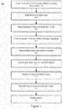
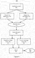
- Figure 1 illustrates an exemplary technique 100 for fabricating an image sensor.
- circuit elements can be created using standard semiconductor processing steps, such as lithography, deposition, ion implantation, annealing, and etching.
- CCD and/or CMOS sensor elements and devices may also be created during step 101.
- These circuit elements are created in an epitaxial layer on the front surface of the wafer and therefore are also called front-side circuit elements.
- the epitaxial (epi) layer is about 20 ⁇ m to 40 ⁇ m thick.
- both the epi layer and the substrate are doped with p-type dopants (such as boron), but the epi layer has a much lower dopant concentration (referred to below and in the figures as p- doping) than the bulk wafer (referred to below and in the figures as p+ doping).
- the epitaxial layer resistivity will be about 10 to 100 ⁇ cm, and the substrate resistivity will be less than about 0.01 ⁇ cm.
- poly-silicon interconnects may be formed in step 101, metal interconnects are generally not because metals will be damaged in subsequent high-temperature processing steps.
- the active sensor areas or even the whole wafer may be thinned from the backside.
- This thinning typically includes a combination of polishing and etching to expose the epi layer.
- the wafer is polished from the backside until the wafer is about 200 ⁇ m to 300 ⁇ m thick.
- a material such as photoresist or other suitable material.
- a chemical etchant is used to etch away the bulk wafer over the active sensor area, thereby exposing the active sensor area. Because the bulk wafer has a much higher dopant concentration and defect density than the epi layer, the etch rate of the bulk semiconductor material is much higher than that of the epi layer.
- the etch process slows down when it reaches the epi layer, thereby resulting in a uniform thickness membrane area.
- the image sensor wafer is bonded to a handle wafer, which might be made of quartz, silicon, sapphire or other material. Then, a polishing process is used to polish the whole wafer until only the epi layer remains.
- a protective layer can be deposited on the front-side surface to protect the front-side circuit elements during steps 107-111.
- any exposed silicon or poly-silicon on the front-side surface must be protected as boron tends to preferentially deposit on silicon.
- step 105 may be performed prior to step 103 so that the protective layer can provide additional protection for the front-side surface during the back-thinning process (step 103).
- the protective layer may comprise a silicon nitride layer deposited, e.g., using plasma-enhanced CVD deposition.
- the back-side surface can be cleaned and prepared for boron deposition. During this cleaning, native oxide and any contaminants, including organics and metals, should be removed from the back-side surface.
- the cleaning can be performed using a dilute HF solution or an RCA clean process (which is a well-known set of wafer cleaning steps including the removal of organic contaminants, the thin oxide layer, and ionic contamination).
- the wafer is preferably dried using the Marangoni drying technique (surface tension based drying technology) or a similar technique to leave the surface dry and free of water marks.
- the wafer is protected in a controlled atmosphere during steps 107-109 (using, e.g. dry nitrogen) to minimize native oxide regrowth.
- the wafer can be held at a high-temperature for a few minutes in a reducing environment, such as a dilute hydrogen gas or a low-pressure hydrogen gas.
- a reducing environment such as a dilute hydrogen gas or a low-pressure hydrogen gas.
- the wafer can be held at a temperature of approximately 800°C for about 4 minutes. This high temperature can remove any native oxide layer that might have regrown following step 107.
- an amorphous layer of pure boron is deposited on the back-side of the back-side surface.
- this deposition can be performed using a mixture of diborane and hydrogen gases at a temperature of about 700-800°C to create a high-purity amorphous boron layer.
- the thickness of the boron layer depends on the intended application for the sensor. Typically, the boron layer thickness is between about 2 nm and 20 nm. The minimum thinness is generally limited by the need for a pinhole-free uniform film. The maximum thickness generally depends on the absorption of the photons or charged particles of interest by the boron.
- steps 109 and 111 can be performed in the same process tool and, preferably, in the same process chamber, thereby ensuring that steps 109 and 111 can be performed in quick succession with no possibility of surface contamination or oxide growth between the steps. More details on boron deposition can be found in " Chemical vapor deposition of a-boron layers on silicon for controlled nanometer-deep p+-n junction formation," Sarubbi et al., J. Electron. Material, vol. 39, pp. 162-173, 2010 .
- the purity and lack of pinholes in the boron layer are critical to the sensitivity and lifetime of the image sensors disclosed herein. If any native oxide film is not removed from the epi layer surface before deposition of the boron, then that native oxide will be affected by DUV, VUV and EUV photons and by charged particles and will cause a degradation of sensor performance with use. Even if all the native oxide is removed prior to the boron deposition, if there are pinholes in the boron layer, then, after processing, oxygen will be able to reach the epi layer through those pinholes and may oxidize the surface of that layer.
- other layers can also be deposited on top of the boron layer during, or immediately following, step 111.
- These other layers may include anti-reflection coatings comprised of one or more materials, such as silicon dioxide, silicon nitride, magnesium fluoride, and lithium fluoride.
- These other layers may also include a protective layer comprising a thin (few nm) layer of a refractory metal. Even though the anti-reflection coating may be affected by DUV, VUV or EUV radiation, the presence of the boron layer between the anti-reflection coating and the epi layer shields the epi layer from charges and traps in the anti-reflection coating and ensures that the sensitivity of the image sensor does not significantly degrade.
- the front-side protective layer can be removed or patterned to prepare for fabrication of interconnects on the front surface.
- this removal/patterning may include etching of the front-side surface in dilute HF, because the boron layer is relatively impervious to dilute HF.
- interconnects on the front surface can be patterned and fabricated. These interconnects may be formed by Al, Cu, or another metal. After interconnect fabrication is complete, a passivation layer may be deposited on the front-side surface to protect these interconnects.
- the completed circuit elements can be packaged.
- the package may include flip-chip bonding or wire bonding of a chip to a substrate.
- the package may include a window that transmits wavelengths of interest, or may comprise a flange or seal for interface to a vacuum seal.
- the package may include other components such as a photocathode as well as a sealed, evacuated tube.
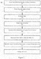
- Figure 2 illustrates an alternative exemplary technique 200 for fabricating an image sensor.
- the circuit elements can be created in step 201 using standard semiconductor processing steps including lithography, deposition, ion implantation, annealing, and etching.
- CCD and/or CMOS sensor elements and devices may also be created in step 201.
- These circuit elements are created in an epi layer on the front-side surface of the wafer.
- the epi layer is about 20 ⁇ m to 40 ⁇ m thick.
- the epi layer has a low dopant concentration (p-).
- interconnects such as metal interconnects, can also be created in step 201.
- step 203 the front-side surface of the wafer can be protected.
- This protection may include depositing one or more protective layers on top of the circuit elements formed during step 201.
- This protection may also, or instead, include attaching the wafer to a handling wafer, such as a silicon wafer, a quartz wafer, or a wafer made of other material.
- Step 205 involves thinning the wafer from the back-side so as to expose the epitaxial layer in, at least, the active sensor areas. This step may involve polishing, etching, or both. In some embodiments, the entire wafer is back-thinned. In other embodiments, only the active sensor areas are thinned all the way to the epitaxial layer.
- Step 207 includes cleaning and preparing the back-side surface prior to the boron deposition. During this cleaning, the native oxide and any contaminants, including organics and metals, should be removed from the back-side surface. In one embodiment, this cleaning can be performed using a dilute HF solution or using an RCA clean process. After cleaning and during preparation, the wafer can be dried using the Marangoni drying technique or a similar technique to leave the surface dry and free of water marks.
- the wafer can be transported to a deposition tool in a protective environment, thereby allowing the wafer to be protected during step 211.
- the protective environment is a dry nitrogen atmosphere, which minimizes native oxide regrowth.
- the time spent to perform step 209 should be kept to a minimum, preferably no more than about five minutes.
- boron is deposited on the back-side surface of the wafer.
- this deposition can be done using a mixture of diborane and hydrogen gases at a temperature of about 400-450°C, thereby creating a high-purity amorphous boron layer.
- the thickness of the deposited boron layer depends on the intended application for the sensor. Typically, the boron layer thickness will be between about 2 nm and 10 nm.
- the minimum thickness is set by the need for a pinhole-free uniform film, whereas the maximum thickness depends on the absorption of the photons or charged particles of interest by the boron, as well as the maximum length of time that the wafer can be kept at the elevated temperature when there are metal interconnects on the front-side.
- other layers may be deposited on the boron layer in step 211.
- These other layers may include anti-reflection coatings comprised of one or more materials such as silicon dioxide, silicon nitride, magnesium fluoride and lithium fluoride.
- These other layers may also include a protective layer comprising a thin layer of a refractory metal. In some embodiments, this refractory metal layer thickness may be between approximately 1 nm and approximately 10 nm.
- the protective front-side layer may be removed in step 213.
- holes or vias can be opened in the protective front-side layer or through-silicon vias around the edges of the device can be exposed, thereby allowing connection to the circuit structures.
- the resulting structure may be packed in a suitable package.
- the packing step may comprise flip-chip bonding or wire bonding of the device to the substrate.
- the package may include a window that transmits wavelengths of interest, or may comprise a flange or seal for interface to a vacuum seal.
- the package may include other components such as the photocathode, and may comprise a sealed, evacuated tube.
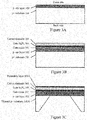
- Figures 3A-3F illustrate exemplary cross-sections of a wafer subjected to method 100 ( Figure 1 ).
- Figure 3A illustrates an epitaxial (epi) layer 302 being formed on the front side of a substrate 301.
- substrate 301 is a p+ (i.e. highly p doped) substrate
- epi layer 302 is a p- epi layer (i.e. a layer with a low concentration of p dopant).
- Figure 3B illustrates a gate oxide layer 303 being formed on epi layer 302, a silicon nitride (Si 3 N 4 ) gate layer 304 being formed on gate oxide layer 303, and front-side circuit elements 305 being formed on gate layer 304 (step 101).
- Si 3 N 4 silicon nitride
- the gate dielectric may comprise one, two, or three layers.
- Forming the front-side circuit elements includes implanting or doping portions of the front side of the epi layer and may involve patterning the gate layer.
- Figure 3C illustrates substrate 301 being thinned at its back-side surface, at least in certain areas, to form thinned substrate 301A (step 103), and a protective layer 305A being formed on front-side circuit elements 305 (step 105).
- Figure 3D illustrates an optional doped layer 302A that may be formed in a portion of epi layer 302 exposed by thinned substrate 301A. This doping may be formed by ion-implantation followed by thermal activation, by plasma doping, by plasma assisted doping or similar techniques.
- this doping can be performed during step 107 as part of the back-side surface preparation and before high-temperature surface treatment in step 109.
- Figure 3E illustrates a pure boron layer 306 being formed on thinned substrate 301A and exposed epi layer 302 (step 111). Since some of the boron diffuses a few nm into the epi layer, some embodiments do not need to include the separately doped layer 303A.
- Figure 3F illustrates that after protective layer 305A is removed or opened (step 113), front-side metal (i.e. interconnect) 307 can be formed on front-side circuit elements 305.
- Figure 3G illustrates one optional embodiment in which a capping layer 308 can be formed on boron layer 306. Capping layer 308 can be formed any time after step 111 (depositing the boron layer), but before step 117 (packaging).
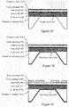
- Figures 4A-4G illustrate exemplary cross-sections of a wafer subjected to method 120 ( Figure 1B ).
- Figure 4A illustrates an epitaxial (epi) layer 402 being formed on the front side of a substrate 401.
- substrate 401 is a p+ substrate
- epi layer 402 is a p- epi layer.
- the substrate is an SOI (silicon-on-insulator) wafer with a buried oxide layer 402A between substrate 401 and epi layer 402. SOI wafers are commercially available from Soitec (Bernin, France) and other suppliers.
- the epi layer is grown directly on the substrate 401 without any buried oxide layer 402A.
- FIG 4B illustrates various circuit elements 403 including interconnects that can be formed on the epi layer (step 121) (note that the epi layer is shown, but not labeled so as not to overly complicate the drawings). Because the interconnects are formed on the wafer prior to back thinning all the way to the epi layer, these interconnects can be formed using normal sub-micron CMOS processing techniques and may include multiple layers of high density metal interconnects. In some embodiments, multiple through-silicon vias (TSV) 403A are created around one, or more, edges of the image sensor array in order to allow connection to the circuit elements 403.
- TSV through-silicon vias
- Figure 4C illustrates a handling wafer 404 attached to the top of the circuit elements 403 (step 123).
- FIG. 4D illustrates the wafer after substrate 401 is back-thinned to epi layer 402. In one embodiment, this back-thinning exposes buried oxide layer 402A.
- Figure 4E illustrates the wafer after a cleaning and preparation of the back-side surface (step 127), which may result in etched oxide 402B being patterned so as to protect TSVs 403A while exposing the epi layer in the image sensor array areas.
- Figure 4F illustrates a pure boron layer 406 after being formed on the back-side surface of the epi layer 402 (step 131).
- an anti-reflection coating or metal coating or capping layer may be deposited on top of the pure boron layer.
- Figure 4G illustrates the wafer after etched oxide 402B is removed and replaced with metal pad 407 so as to allow electrical connection to the TSV 403A (step 131).
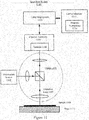
- FIG. 5 illustrates an exemplary electron-bombarded image sensor system 501.
- the whole assembly can be contained in a sealed tube 505 (e.g. substantially similar to the sealed tube of standard image intensifier and electron-bombarded CCD (EBCCD) devices).
- a top surface 507 of the tube 505 can include a window that is transparent at the wavelengths of interest.
- this window preferably comprises a very pure grade of quartz, fused silica or alumina (sapphire).
- the outside surface of the window is coated with a UV anti-reflection coating.
- a coating might comprise a single layer of a low index material such as MgF 2 , or might comprise a multi-layer coating.
- photocathode 504. Coated on the inside surface of the window, or placed immediately adjacent to that inside surface, is a photocathode 504.
- the photocathode material may be substantially similar to any photocathode material known in the art for use in photomultiplier, image intensifier, or prior-art EBCCD detectors.
- the photocathode may comprise one or more alkali metals such as cesium, and/or may comprise a semiconductor such GaN, GaAs, or silicon.
- Photocathode 504 can be held at a negative voltage 503 relative to a solid-state image sensor 502, which is positioned near the bottom surface of sealed tube 505.
- negative voltage 503 may be approximately 500 V; in other embodiments, it may be a few hundred volts or approximately 1000 V. In preferred embodiments, negative voltage 503 is between 100 V and 1500 V.
- Solid-state image sensor 502 can be a thinned CCD or CMOS image sensor oriented so that the electrons impinge first on its back-side surface.
- the back-side of solid-state image sensor 502 includes a layer of boron deposited directly on the epi layer of the image array as described above.
- a thin (few nm) layer of a conductive material, such as a refractory metal, is deposited on the boron layer to prevent charge-up of the sensor surface.
- solid-state image sensor 502 is a time-delay integration (TDI) CCD.
- solid-state image sensor 502 comprises a linear array of electron-sensitive elements.
- solid-state image sensor 502 comprises a two-dimensional array of electron sensitive elements.
- solid-state image sensor 502 is held close to ground potential (shown).
- photoelectrons 520 When light 510 is incident on the electron-bombarded image sensor system 501, one or more photoelectrons 520 are emitted from photocathode 504. These photoelectrons are emitted in substantially all directions, but they are accelerated towards solid-state image sensor 502 by the potential difference between photocathode 504 and solid-state image sensor 502.
- the gap between photocathode 504 and solid-state image sensor 502 is less than 1 mm. In some embodiments, the gap is approximately 500 ⁇ m.
- Incorporating solid-state image sensor 502 having one of the structures and/or fabricated in accordance with any of the methods described herein enables electron-bombarded image sensor system 501 to operate with a low potential difference between photocathode 504 and solid-state image sensor 502, and yet have high gain because electrons are more easily able to penetrate through the boron layer than through a silicon dioxide layer. Because boron-doped silicon, boron silicide, and boron are all at least partially conductive, charging of the surface under electron bombardment is minimized or avoided. The sensitivity to charge up can be further reduced by a conductive or metallic layer on top of the boron layer as described herein.
- the gap between the photocathode and the image sensor is typically 1-2 mm.
- Such a large gap allows significant transverse motion of the electrons as they travel from the photocathode to the image sensor due to energy of the electrons as they emerge from the photocathode.
- a gap of 1-2 mm or more is necessary because of the large potential difference between the photocathode and the image sensor (typically about 2000 V or more). Reducing the potential difference between the photocathode and the image sensor allows a smaller gap to be used.
- the lower energy of the electrons means that there is less spreading of the electrons created within the solid-state image sensor.
- the low energy of the electrons arriving at solid-state image sensor 502 means that the probability of atoms being ablated from the surface of solid-state image sensor 502 is low to zero. Furthermore, the energy of the electrons arriving at solid state image sensor 502 is not enough to generate X-rays from the silicon, thereby avoiding the generation of spurious signal in nearby pixels of image sensor 502.
- Collisions of low energy electrons with residual gas atoms in the vacuum created in sealed tube 505 will generate fewer ions as compared with high energy electrons. Furthermore, due to the low potential difference between photocathode 504 and solid-state image sensor 502, those ions will have less kinetic energy when they strike the photocathode and will ablate less photocathode material.
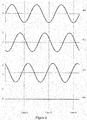
- Figure 6 illustrates exemplary driving voltages for the clock signals of any of the image sensors described herein that incorporate CCDs.
- charge needs to be transferred from one storage element to another until the charge reaches the output amplifier.
- Multiple clock signals are needed to transfer the charge.
- those clock signals are sinusoidal, or substantially sinusoidal, in shape, in preference to substantially square waveforms used in traditional CCD devices, The advantages of using sinusoidal waveforms are that the charge transfer is smoother (which is particularly an advantage in allowing TDI sensors to track the motion of the image more accurately), and the clock signals generate less electrical noise and heat because of the minimal content of harmonics of the fundamental frequency.
- FIG. 6 illustrates the clock voltages for a 3-phase CCD.
- Clock signal 601 shows the voltage on the first clock signal as a function of time.
- Clock signal 601 is a substantially sinusoidal waveform.
- the second clock signal 602 also has a voltage that varies as a function of time, but is substantially 120° phase-delayed with respect to clock signal 601.
- the voltage of the third clock signal 603 also varies as a function of time, but is substantially 120° phase-delayed with respect to clock signal 602, and hence substantially 240° phase-delayed with respect to clock signal 601.
- Line 604 illustrates the sum of the three clock signals 601, 602, and 603, which is substantially zero all the time.
- the substantially zero sum voltage means that little current from the clock signals flows in the ground signal of solid-state image sensor 502, thereby resulting in lower electrical noise levels. This is in contrast to the sum of three out-of-phase square-wave clock signals, which would have non-zero sums voltages essentially all the time.
- the two clock signals In an image sensor including a 2-phase CCD (not shown), the two clock signals would be substantially 180° out of phase with one another.
- the second clock signal In a 4-phase CCD (not show), the second clock signal would be substantially 90° phase-delayed with respect to the first clock signal, the third clock signal would be substantially 180° phase-delayed with respect to the first clock signal, and the fourth clock signal would be substantially 270° phase-delayed with respect to the first clock signal.
- Figure 7A illustrates an exemplary split-readout image sensor 700 including two sets of readout circuits 701A and 701B positioned on either side of an image region 703.
- Image region 703 includes a pure boron layer on its light sensitive surface as described herein.
- Readout circuits 701A and 701B can include serial registers 702A and 702B and readout amplifiers 704A and 704B, as well as other components such as transfer gates.
- Exemplary embodiments of readout circuits 701A and 701B, as well as other components of sensor 700 are described in U.S. Patent 7,609,309 , entitled “Continuous Clocking of TDI Sensors", issued October 27, 2009, which is incorporated by reference herein.
- Image region 703 is a two-dimensional (2D) array of pixels, and each line of the image is read out concurrently in each direction A and B. Each line is then read out one pixel at a time in the simplest case. Therefore, in preferred embodiments, the serial registers 702A and 702B can be divided into a plurality of register segments (e.g. Figure 7A shows each serial register being divided into six segments, thereby allowing parallel read out using a plurality of amplifiers 704A and 704B.
- readout circuits 701A and 701B can be operated independently, thereby allowing image sensor 700 to provide two readout directions A and B.
- each side of image region 703 i.e. sides 703A and 703B
- image region 703 may have 1000 lines, each line formed by a column of pixels. Therefore, during the split-readout mode, 500 lines could be read out in direction A and, concurrently, 500 lines could be read out in direction B.
- CCD drivers charge-coupled device
- a plurality of CCD drivers P1a, P2a, P3a, P1b, P2b, and P3b can be used to provide phases.
- CCD drivers P1a, P2a, P3a, P1b, P2b, and P3b can be characterized as driving sets of gate electrodes (hereinafter gates), each set having six gates.
- gates are provided for each pixel to provide three phases.
- pixels 710 and 711 are shown, wherein gates 731, 732, and 733 are positioned over pixel 710 and gates 734, 735, and 736 are positioned over pixel 711.
- pixels 710 and 711 are aligned along the read-out axis to form part of a column of the 2D array of pixels forming image region 703.
- Image region 703 can be implemented as an optical sensor or a charged particle sensor.
- image region 703 can include a photo-sensitive p-type silicon substrate 714 and an n-type buried channel 713.
- the electrostatic forces in silicon substrate 714 are determined by the voltage level applied to a particular gate by a clock input signal (e.g. one of clock signals from CCD drivers P1a, P2a, P3a, P1b, P2b, and P3b).
- a clock input signal e.g. one of clock signals from CCD drivers P1a, P2a, P3a, P1b, P2b, and P3b.
- High level voltages induce the formation of a potential "well" beneath the gate, whereas low level voltages form a potential barrier to electron movement.
- a gate voltage is driven high when an adjacent gate voltage is driven low.
- gates 731 and 734 of pixels 710 and 711 respectively, have high level voltages that form potential wells with integrated charge (i.e. electrons), and gates 732, 733 (of pixel 710) and 735, 736 (of pixel 711) have low level voltages that form potential barriers.
- gates 732 and 735 of pixels 710 and 711 respectively, have high level voltages that form potential wells with integrated charge (i.e. electrons), and gates 731, 733 (of pixel 710) and 734, 736 (of pixel 711) have low level voltages that form potential barriers.
- gates 733 and 736 of pixels 710 and 711 respectively, have high level voltages that form potential wells with integrated charge (i.e. electrons), and gates 731, 732 (of pixel 710) and 734, 735 (of pixel 711) have low level voltages that form potential barriers.
- adjacent gates when shifting charge preferably both have a high level voltage for a short time to facilitate charge transfer.
- the charge is shifted from left to right, i.e. from pixel 710 to pixel 711.
- a similar directional shifting of charge can be take place from time 771 to time 772.
- split-readout image sensor 700 Additional details of split-readout image sensor 700 are provided in US Provisional Patent Application 61/735,427 , entitled “METHOD AND APPARATUS FOR HIGH SPEED ACQUISITION OF MOVING IMAGES USING PULSED ILLUMINATION", filed by David Brown et al. on December 10, 2012, and incorporated by reference herein. Additional details regarding other exemplary image sensors are provided in US Patent 7,528,943 entitled METHOD AND APPARATUS FOR SIMULTANEOUS HIGH-SPEED ACQUISITION OF MULTIPLE IMAGES” by Brown et al., issued May 5, 2009, and incorporated by reference herein.
- Figure 8 shows a reticle, photomask or wafer inspection system 800 that simultaneously detects two channels of image or signal on one sensor 870.
- Image sensor 870 comprises a split-readout image sensor as described above.
- Illumination source 809 may incorporate a 193 nm or sub-200-nm laser.
- the two channels may comprise reflected and transmitted intensity when an inspected object 830 is transparent (for example a reticle or photomask), or may comprise two different illumination modes, such as angles of incidence, polarization states, wavelength ranges or some combination thereof.
- the light is directed to inspected object 830 using channel one illumination relay 815 and channel two illumination relay 820.
- the inspected object 830 may be a reticle, a photomask, a semiconductor wafer or other article to be inspected.
- Image relay optics 840 can direct the light that is reflected and/or transmitted by inspected object 830 to a channel one image mode relay 855 and to a channel two image mode relay.
- Channel one image mode relay 855 is tuned to detect the reflection/transmission corresponding to channel one illumination illumination relay 815
- channel two image mode relay sensor 860 is tuned to detect the reflection/transmission corresponding to channel two illumination relay 820.
- Channel one image mode relay 855 and channel two image mode relay sensor 860 in turn direct their outputs to sensor 870.
- the data corresponding to the detected signals or images for the two channels is shown as data 890 and is transmitted to a computer (not shown) for processing.
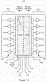
- Figure 9 illustrates an exemplary detector assembly 900 incorporating an image sensor 904, a silicon interposer 902 and other electronics in accordance with certain embodiments of the present invention.
- the detector assembly 900 may include one or more light sensitive sensors 904 disposed on the surface of an interposer 902.
- the one or more interposers 902 of the assembly 100 may include, but are not limited to, a silicon interposer.
- the one or more light sensitive sensors 904 of the assembly 900 are back-thinned and further configured for back-illumination including a boron layer deposited on the back surface as described above.
- various circuit elements of the assembly 900 may be disposed on or built into the interposer 902.
- one or more amplification circuits e.g., charge conversion amplifier
- one or more conversion circuits 908 e.g., analog-to-digital conversion circuits, i.e. digitizers 908
- one or more driver circuits 906 may be disposed on or built into the interposer 902.
- the one or more driver circuits 906 may include a timing/serial drive circuit.
- the one or more driver circuits 906 may include, but are not limited to, clock driver circuitry or reset driver circuitry.
- one or more decoupling capacitors may be disposed on or built into the interposer 902.
- one or more serial transmitters maybe disposed on or built into the interposer 102.
- one or more support structures may be disposed between the bottom surface of the light sensitive array sensor 904 and the top surface of the interposer 902 in order to provide physical support to the sensor 904.
- a plurality of solder balls 916 may be disposed between the bottom surface of the light sensitive array sensor 904 and the top surface of the interposer 902 in order to provide physical support to the sensor 904. It is recognized herein that while the imaging region of the sensor 904 might not include external electrical connections, the back-thinning of the sensor 904 causes the sensor 904 to become increasingly flexible. As such, solder balls 916 may be utilized to connect the sensor 904 to the interposer 902 in a manner that reinforces the imaging portion of the sensor 904.
- an underfill material may be disposed between the bottom surface of the light sensitive array sensor 904 and the top surface of the interposer 902 in order to provide physical support to the sensor 904.
- an epoxy resin may be disposed between the bottom surface of the light sensitive array sensor 904 and the top surface of the interposer 902.
- the interposer 902 and the various additional circuitry are disposed on a surface of a substrate 910.
- the substrate 910 includes a substrate having high thermal conductivity (e.g., ceramic substrate).
- the substrate 910 is configured to provide physical support to the sensor 904/interposer 902 assembly, while also providing a means for the assembly 900 to efficiently conduct heat away from the imaging sensor 904 and the various other circuitry (e.g., digitizer 906, driver circuitry 908, amplifier, and the like).
- the substrate may include any rigid highly heat conductive substrate material known in the art.
- the substrate 910 may include, but is not limited to, a ceramic substrate.
- the substrate 110 may include, but is not limited to, aluminum nitride.
- the substrate 910 may be configured to provide an interface to a socket or an underlying printed circuit board (PCB).
- PCB printed circuit board
- the substrate 910 may provide interconnection between the interposer 902 and a socket or a PCB via interconnects 912.
- the substrate 910 may be operatively coupled to an underlying PCB and further electrically coupled to a socket or PCB in a variety of ways, all of which are interpreted to be within the scope of the present invention.
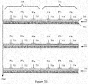
- FIG. 10 illustrates an exemplary sensor module array 1000 including a plurality of time delay integration (TDI) sensor modules 1001.
- Each sensor module 1001 includes one of the above-described image sensors.
- the image sensors may have a few nm (such as 1 or 2 nm) thick coating of Ru or other refractory metal on top of the boron in order to protect the boron during cleaning.
- each TDI sensor module 1001 can include localized driving and signal processing circuitry.
- This circuitry can include a TDI sensor (the center block), processing circuits for processing the signals from the TDI sensor, timing and serial drive circuits, and pixel gate driver circuits.
- the driving/processing circuits are positioned around the TDI sensor.
- the TDI sensors in adjacent rows can be aligned such that at least 100% image coverage is achieved when used in a continuous scanning configuration,
- the upper row 1002 can be offset with respect to the lower row 1004 such that the TDI sensor is positioned in the gap produced by the driving/processing circuits of an adjacent row.
- the width of each TDI sensor is equal to or greater than the space between TDI sensors.
- sensor module array 1000 can ensure 100% EUV wavelength image capture.
- some minimal overlap between TDI sensors from adjacent rows can provide redundant data. This redundant data can, for example, ensure accurate alignment of the image data generated by TDI sensor modules 1001.
- the inspection system can arbitrarily select the data from one TDI sensor module to be used for the edge pixels.
- a detection system can combine and align, using sub-pixel digital processing, the data from multiple TDI sensor modules, to achieve improved quality data near edge pixels.
- Figure 11 illustrates an exemplary inspection system 1100 configured to measure a sample 1108 such as a wafer, reticle, or photomask.
- Sample 1108 is placed on a stage 1112 in facilitate movement to different regions of sample 1108 underneath the optics.
- Stage 1112 may comprise an X-Y stage or an R- ⁇ stage.
- stage 1112 can adjust the height of sample 1108 during inspection to maintain focus.
- an objective lens 1105 can be adjusted to maintain focus.
- An illumination source 1102 may comprise one or more lasers and/or a broad-band light source. Illumination source 1102 may emit DUV and/or VUV radiation. Optics 1103 including an objective lens 1105 can direct that radiation towards, and focuses it on, sample 1108. Optics 1103 may also comprise mirrors, lenses, and/or beam splitters. Light reflected or scattered from sample 1108 can be collected, directed, and focused by optics 1103 onto a detector 1106, which is within a detector assembly 1104.
- Detector 1106 may include one, or more, of the image sensors described herein, including boron-coated back-illuminated CCD sensors, boron-coated back-illuminated CMOS sensors, and electron-bombarded images sensors incorporating a boron-coated back-thinned solid state image sensor.
- Detector 1106 may include a two-dimensional array sensor or a one-dimensional line sensor.
- the output of detector 1106 can be provided to a computing system 1114, which analyzes the output.
- Computing system 1114 can be configured by program instructions 1118, which can be stored on a carrier medium 1116.
- illumination source 1102 may be a continuous source such as an arc lamp, a laser-pumped plasma light source, or a CW laser.
- illumination source 1102 may be a pulsed source such as a mode-locked laser, a Q-switched laser, or a plasma light source pumped by a Q-switched laser.
- the image sensor or sensors within detector 1106 are synchronized with the laser pulses. In such embodiments, the image sensor may operate in a TDI mode during the laser pulse and then may readout the data through multiple outputs on both sides of the sensor in between laser pulses.
- inspection system 1100 illuminate a line on sample 1108, and collect scattered and/or reflected light in one or more dark-field and/or bright-field collection channels.
- the image sensor may be a line sensor or an electron-bombarded line sensor.
- inspection system 1100 illuminate multiple spots on sample 1108, and collect scattered and/or reflected light in one or more dark-field and/or bright-field collection channels.
- the image sensor may be a two-dimensional array sensor or an electron-bombarded two-dimensional array sensor.
- Patent 5,999,310 by Shaker et al., which issued on December 7, 1999
- U.S. Patent 7,525,649 by Leong et al., which issued on April 28, 2009 . All of these patents and patent applications are incorporated by reference herein.
Abstract
Description
- The present application claims priority to
US Provisional Application 61/622,295 US Provisional Application 61/658,758 - The present application is also related to
US Patent Application 13/710,31561/569,611 US Provisional Application 61/735,427 - The present application relates to image sensors suitable for sensing radiation in deep UV (DUV), vacuum UV (VUV), and extreme UV (EUV) wavelength, and to methods for making such image sensors. Some embodiments of the sensors are suitable for sensing electrons and other charged particles. All of the sensors are suitable for use in photomask, reticle, or wafer inspection systems.
- The integrated circuit industry requires inspection tools with increasingly higher resolution to resolve ever smaller features of integrated circuits, photomasks, reticles, solar cells, charge coupled devices etc., as well as detect defects whose sizes are of the order of, or smaller than, those feature sizes.
- Inspection systems operating at short wavelengths, e.g. wavelengths shorter than about 250 nm, can provide such resolution in many cases. In other cases, electrons or other charged particles, such as helium (He) nuclei (i.e. alpha particles) may be used. Specifically, for photomask or reticle inspection, it is desirable to inspect using a wavelength identical, or close, to the wavelength that will be used for lithography, i.e. close to 193.4 nm for current generation lithography and close to 13.5 nm for future EUV lithography, as the phase-shifts of the inspection light caused by the patterns will identical or very similar to those caused during lithography. For inspecting semiconductor patterned wafers, inspection systems operating over a relatively broad range of wavelengths, such as a wavelength range that includes wavelengths in the near UV, DUV, and/or VUV ranges, can be advantageous because a broad range of wavelengths can reduce the sensitivity to small changes in layer thicknesses or pattern dimensions that can cause large changes in reflectivity at an individual wavelength.
- In order to detect small defects or particles on photomasks, reticles, and semiconductor wafers, high signal-to-noise ratios are required. High photon or particle flux densities are required to ensure high signal-to-noise ratios when inspecting at high speed because statistical fluctuations in the numbers of photons detected (Poisson noise) is a fundamental limit on the signal-to-noise ratio. In many cases, approximately 100,000 or more photons per pixel are needed. Because inspection systems are typically in use 24 hours per day with only short stoppages, the detectors are exposed to large doses of radiation after only a few months of operation.
- A photon with a vacuum wavelength of 250 nm has energy of approximately 5 eV. The bandgap of silicon dioxide is about 10 eV. Although it would appear that such wavelength photons cannot be absorbed by silicon dioxide, silicon dioxide as grown on a silicon surface must have some dangling bonds at the interface with the silicon because the silicon dioxide structure cannot perfectly match that of the silicon crystal. Furthermore, because the single dioxide is amorphous, there are likely also some dangling bonds within the material. In practice, there will be a non-negligible density of defects and impurities within the oxide, as well as at the interface to underlying semiconductor, that can absorb photons with deep UV wavelengths, particularly those shorter than about 250 nm in wavelength. Furthermore, under high radiation flux density, two high-energy photons may arrive near the same location within a very short time interval (nanoseconds or picoseconds), which can lead to electrons being excited to the conduction band of the silicon dioxide by two absorption events in rapid succession or by two-photon absorption. EUV photons have very high energies (13.5 nm in wavelength corresponds to photon energy close to 92 eV) and are capable of breaking silicon-oxygen bonds as well as strongly interacting with defects and contaminants in the oxide. Electron and charged-particle detectors typically have to detect electrons or charged particles with energies of a few hundred eV or higher. Energies greater than 10 eV can readily break silicon-oxygen bonds.
- As indicated above, high-energy photons and particles can break bonds and ionize atoms in a silicon dioxide layer. Because silicon dioxide is a good insulator, free electrons created in the silicon dioxide may have lifetimes of ms or longer before recombining. Some of these electrons may migrate into the semiconductor material. These electrons create electric fields within the silicon dioxide and between the silicon dioxide and semiconductor. These electric fields can cause electrons created in the semiconductor by absorption of photons to migrate to the surface of the semiconductor and recombine, thereby resulting in lost signal and reduced detector quantum efficiency. Near continuous use of the instrument means that there may be little, or no, time for recovery of the detector, as new free charges are created as fast as, or faster than, they can recombine.
- High-energy particles and photons can also cause irreversible changes to the silicon dioxide. Such changes can include reconfiguration of the bonding of atoms or migration of small atoms within the silicon dioxide. At normal operating temperatures of the detector, which are typically in a range from around room temperature to about 50°C, these changes will not recover. In particular, it is known that conventional silicon photodiodes used as EUV detectors degrade in efficiency with use.
- The silicon dioxide layer on the surface of semiconductor detectors significantly reduces the efficiency of those detectors for low-energy (less than about 2 kV) electrons. Some low-energy electrons are absorbed by the silicon dioxide, thereby causing the silicon dioxide to charge up and deflect subsequent arriving electrons. Because a native oxide will always form on an exposed silicon surface, silicon detectors necessarily must have some oxide on their surface. Growing or depositing an alternative dielectric material (instead of the oxide) on the surface of the semiconductor results in a much higher density of defect states at the semiconductor to silicon dioxide interface. These defects reduce the quantum efficiency of the detector, especially for photons or charged particles absorbed close to the surface of the semiconductor.
- An additional cause of degradation of EUV sensors is that, in a EUV system, a thin layer of carbon builds up over time on any surface exposed to EUV radiation, including the surface of the image sensors and optical elements. This carbon layer, as it becomes thicker, absorbs EUV radiation and reduces the sensitivity of the sensor, as well as reducing the reflectivity of optical elements in the light path. In a EUV system, all surfaces exposed to EUV are periodically cleaned to remove the carbon. This cleaning is usually performed with activated hydrogen (a mixture of atomic hydrogen and hydrogen radicals), which is very effective at removing carbon. However hydrogen radicals affect the oxide on the surface of silicon detectors and can also cause degradation of the performance of those sensors.
- Diode detectors suitable for detecting EUV and/or electrons are known in the art. Exemplary diode detectors are described in
US Patent 8,138,485 issued to Nihtianov on March 20, 2012 ,US Patent 7,586,108 issued to Nihtianov on September 8, 2009 ,US Published Application 2012/0268722 published on October 25, 2012 (filed by Nihtianov ), andUS Published Application 2011/0169116 published on July 14, 2011 (filed by Nanver ), These diode detectors include a thin (1nm to 20nm) layer of boron directly on the silicon surface.US Published Application 2011/0169116 further describes an open mesh of a metallic conductor on the surface of such a detector. - These prior-art detectors have contacts formed on the top (light or electron-incident) surface. A disadvantage of having contacts and conductors formed on the illuminated surface is that it is not possible to create a detector with a large number (thousands or millions) of detector elements (pixels) while maintaining high detector efficiency. Each detector element requires multiple control signals, which are typically shared with other detector elements. For full-well capacities of 100,000 electrons or more, detector element dimensions may typically be in the range of about 10 µm to 20 µm. It is not possible to make hundreds or thousands of interconnects that connect these control signals to one another and to drive circuits without covering a substantial fraction of the area of the surface. Because DUV, VUV, and EUV photons and low-energy particles will not penetrate through layers of conductors such as metals and poly-silicon, the area covered by these conductors will have low, or no, sensitivity.
- Therefore, a need arises for an image sensor capable of detecting high-energy photons or charged particles yet overcoming the above disadvantages.
- Methods of fabricating image sensors with high-quantum-efficiency for imaging DUV, VUV, and/or EUV radiation and/or charged particles are described. Image sensors fabricated according to these methods are capable of long-life operation under high fluxes of DUV, VUV, EUV, and/or charged particles. These methods include process steps to form light sensitive active and/or passive circuit elements in a layer on a semiconductor (preferably silicon) wafer.
- An exemplary method of fabricating an image sensor includes forming an epitaxial layer on a substrate, forming a gate layer on the epitaxial layer, the gate layer comprising one or more layers of dielectric materials such as silicon dioxide and silicon nitride, forming circuit elements on the gate layer comprising poly-silicon and dielectric materials, but no metal films or metal interconnects, thinning the substrate to generate a thinned substrate (also referred to herein as a membrane) and expose at least portions of the epitaxial layer, and forming a pure boron layer directly on the exposed portions of the epitaxial layer. As used herein, the phrase "circuit elements" refers to light sensitive devices such as charge-coupled devices and photodiodes, other semiconductor devices such as transistors, diodes, resistors and capacitors, and electrical interconnections (often called interconnects) between them. In this first exemplary embodiment, the circuit elements formed prior to boron deposition do not include any metal interconnects. These circuit elements are formed using standard semiconductor manufacturing processes including, but not limited to, photolithography, deposition, etching, ion implantation and annealing. Thinning the sample (e.g. a wafer) can be performed using chemical etching and/or polishing. Notably, this thinning can increase the sensitivity of the image sensor to light impinging the back surface. An anti-reflection coating or a conductive coating can be formed on the boron layer. This anti-reflection or conductive coating may increase the transmission of wavelengths of interest into the image sensor and/or protect the image sensor. In one embodiment, at least one exposed portion of the epitaxial layer can be doped after thinning the substrate and before forming the boron layer. After the boron layer has been deposited on the back surface, the circuits on the front surface can be completed, including forming metal interconnects.
- Another method of fabricating an image sensor includes forming an epitaxial layer on a substrate, then forming circuit elements on the epitaxial layer. This step may include forming metal interconnects. Either a handling wafer or a protective layer can be formed on the circuit elements. The substrate is then thinned to expose, at least part of, the epitaxial layer. As indicated above, this thinning can increase the sensitivity of the image sensor to light impinging on the back surface. A pure boron layer is formed on the surface of the epitaxial layer exposed in the thinning process. An anti-reflection coating or a conductive coating can be formed on the boron layer. This anti-reflection or conductive coating may increase the transmission of wavelengths of interest into the image sensor and/or protect the image sensor.
- Image sensors with high-quantum-efficiency and long-life operation for DUV, VUV, and/or EUV radiation and/or charged particles are described. These image sensors are thinned from the back-side so that they are highly sensitive to radiation or charged particles impinging on the back-side of the image sensors (wherein these image sensors are back-illuminated). Deposited directly on the back surface of the epitaxial layer is a thin (e.g. between about 2 nm and about 20 nm thick) layer high-purity amorphous boron. In some embodiments, an additional layer of material may be coated on the boron. The thickness and material of each layer may be chosen to increase the transmission of wavelength of interest into the image sensor and/or to protect the image sensor.
- The image sensors described herein may be fabricated using CCD (charge coupled device) or CMOS (complementary metal oxide semiconductor) technology. The image sensors may be two-dimensional area sensors, or one dimensional array sensors.
- An electron-bombarded image sensor is described herein. The electron-bombarded image sensor includes a photocathode that emits electrons when it absorbs a photon or charged particle. Emitted electrons are accelerated towards a solid-state image sensor, such as a CCD image sensor or a CMOS image sensor. The image sensor includes a pure boron layer deposited directly on a thinned substrate, as described above, thereby ensuring that almost all the electrons striking it penetrate into the device. This high level of penetration enables the electron-bombarded image sensor to use a low accelerating voltage (such as an accelerating voltage that is less than 2 kV, or less than 1 kV), thereby resulting in better image resolution and longer sensor lifetime.
- A system for inspecting a sample is also described. This system includes an illumination source and two illumination relays for illuminating the sample. Image relay optics are configured to direct light outputs, i.e. reflections and/or transmissions, of the sample to a first channel image mode relay when the light outputs correspond to the first channel illumination relay, and to a second channel image mode relay when the light outputs correspond to the second channel illumination relay. A sensor is configured to receive relay outputs of the first channel image mode relay and the second channel image mode relay. The sensor includes a semiconductor membrane, in which circuit elements are formed on one surface of the membrane and a boron layer is deposited on the opposite surface of the membrane. In this configuration, the sensor is capable of simultaneously detecting two images of the same sample.
- An exemplary inspection system is also described. This inspection system includes an illumination source, optics, and a detector. The optics are configured to direct and focus radiation from the illumination source onto a sample. The detector is configured to receive reflected or scattered light from the sample, wherein the optics are further configured to collect, direct, and focus the reflected or scattered light onto the detector. The detector can include one or more image sensors. At least one image sensor includes a semiconductor membrane, wherein the semiconductor membrane includes circuit elements formed on one surface of the semiconductor membrane and a boron layer is deposited on the opposite surface of the semiconductor membrane.
-
-
Figure 1 illustrates an exemplary method of fabricating an image sensor. -
Figure 2 illustrates an alternative exemplary technique 120 for fabricating an image sensor. -
Figures 3A-3G illustrate exemplary cross-sections of a wafer subjected to the method described in reference toFigure 1 . -
Figures 4A-4G illustrate exemplary cross-sections of a wafer subjected to the method described in reference toFigure 2 . -
Figure 5 illustrates an exemplary electron-bombarded image sensor system. -
Figure 6 illustrates exemplary driving voltages for the clock signals of any of the image sensors described herein that incorporate CCDs. -
Figure 7A illustrates an exemplary split-readout image sensor including two sets of readout circuits. -
Figure 7B illustrates a plurality of CCD drivers driving sets of gate electrodes, each set having multiple gates. -
Figure 8 shows a reticle, photomask or wafer inspection system that can simultaneously detect two channels of image or signal on one sensor. -
Figure 9 illustrates an exemplary detector assembly incorporating an image sensor, a silicon interposer, and other electronics. -
Figure 10 illustrates an exemplary sensor module array including a plurality of time delay integration (TDI) sensor modules. -
Figure 11 illustrates an exemplary inspection system configured to measure a sample such as a wafer, reticle, or photomask. -
Figure 1 illustrates anexemplary technique 100 for fabricating an image sensor. Instep 101, circuit elements can be created using standard semiconductor processing steps, such as lithography, deposition, ion implantation, annealing, and etching. CCD and/or CMOS sensor elements and devices may also be created duringstep 101. These circuit elements are created in an epitaxial layer on the front surface of the wafer and therefore are also called front-side circuit elements. In preferred embodiments, the epitaxial (epi) layer is about 20 µm to 40 µm thick. In preferred embodiments, both the epi layer and the substrate are doped with p-type dopants (such as boron), but the epi layer has a much lower dopant concentration (referred to below and in the figures as p- doping) than the bulk wafer (referred to below and in the figures as p+ doping). Typically the epitaxial layer resistivity will be about 10 to 100 Ω cm, and the substrate resistivity will be less than about 0.01 Ω cm. Although poly-silicon interconnects may be formed instep 101, metal interconnects are generally not because metals will be damaged in subsequent high-temperature processing steps. - In
step 103, the active sensor areas or even the whole wafer may be thinned from the backside. This thinning typically includes a combination of polishing and etching to expose the epi layer. In one embodiment, the wafer is polished from the backside until the wafer is about 200 µm to 300 µm thick. Then, the front surface and the frame areas around the active sensor areas are protected with a material, such as photoresist or other suitable material. At this point, a chemical etchant is used to etch away the bulk wafer over the active sensor area, thereby exposing the active sensor area. Because the bulk wafer has a much higher dopant concentration and defect density than the epi layer, the etch rate of the bulk semiconductor material is much higher than that of the epi layer. The etch process slows down when it reaches the epi layer, thereby resulting in a uniform thickness membrane area. In another embodiment, the image sensor wafer is bonded to a handle wafer, which might be made of quartz, silicon, sapphire or other material. Then, a polishing process is used to polish the whole wafer until only the epi layer remains. - In
step 105, a protective layer can be deposited on the front-side surface to protect the front-side circuit elements during steps 107-111. In particular, any exposed silicon or poly-silicon on the front-side surface must be protected as boron tends to preferentially deposit on silicon. In some embodiments,step 105 may be performed prior to step 103 so that the protective layer can provide additional protection for the front-side surface during the back-thinning process (step 103). In some embodiments, the protective layer may comprise a silicon nitride layer deposited, e.g., using plasma-enhanced CVD deposition. - In
step 107, the back-side surface can be cleaned and prepared for boron deposition. During this cleaning, native oxide and any contaminants, including organics and metals, should be removed from the back-side surface. In one preferred embodiment, the cleaning can be performed using a dilute HF solution or an RCA clean process (which is a well-known set of wafer cleaning steps including the removal of organic contaminants, the thin oxide layer, and ionic contamination). After cleaning and during preparation, the wafer is preferably dried using the Marangoni drying technique (surface tension based drying technology) or a similar technique to leave the surface dry and free of water marks. In preferred embodiments, the wafer is protected in a controlled atmosphere during steps 107-109 (using, e.g. dry nitrogen) to minimize native oxide regrowth. - In step 109, the wafer can be held at a high-temperature for a few minutes in a reducing environment, such as a dilute hydrogen gas or a low-pressure hydrogen gas. In preferred embodiments, the wafer can be held at a temperature of approximately 800°C for about 4 minutes. This high temperature can remove any native oxide layer that might have regrown following
step 107. - In
step 111, an amorphous layer of pure boron is deposited on the back-side of the back-side surface. In one preferred embodiment, this deposition can be performed using a mixture of diborane and hydrogen gases at a temperature of about 700-800°C to create a high-purity amorphous boron layer. The thickness of the boron layer depends on the intended application for the sensor. Typically, the boron layer thickness is between about 2 nm and 20 nm. The minimum thinness is generally limited by the need for a pinhole-free uniform film. The maximum thickness generally depends on the absorption of the photons or charged particles of interest by the boron. Note that steps 109 and 111 can be performed in the same process tool and, preferably, in the same process chamber, thereby ensuring thatsteps 109 and 111 can be performed in quick succession with no possibility of surface contamination or oxide growth between the steps. More details on boron deposition can be found in "Chemical vapor deposition of a-boron layers on silicon for controlled nanometer-deep p+-n junction formation," Sarubbi et al., J. Electron. Material, vol. 39, pp. 162-173, 2010. - The purity and lack of pinholes in the boron layer are critical to the sensitivity and lifetime of the image sensors disclosed herein. If any native oxide film is not removed from the epi layer surface before deposition of the boron, then that native oxide will be affected by DUV, VUV and EUV photons and by charged particles and will cause a degradation of sensor performance with use. Even if all the native oxide is removed prior to the boron deposition, if there are pinholes in the boron layer, then, after processing, oxygen will be able to reach the epi layer through those pinholes and may oxidize the surface of that layer.
- In some embodiments, other layers can also be deposited on top of the boron layer during, or immediately following,
step 111. These other layers may include anti-reflection coatings comprised of one or more materials, such as silicon dioxide, silicon nitride, magnesium fluoride, and lithium fluoride. These other layers may also include a protective layer comprising a thin (few nm) layer of a refractory metal. Even though the anti-reflection coating may be affected by DUV, VUV or EUV radiation, the presence of the boron layer between the anti-reflection coating and the epi layer shields the epi layer from charges and traps in the anti-reflection coating and ensures that the sensitivity of the image sensor does not significantly degrade. - In
step 113, the front-side protective layer can be removed or patterned to prepare for fabrication of interconnects on the front surface. In some embodiments, this removal/patterning may include etching of the front-side surface in dilute HF, because the boron layer is relatively impervious to dilute HF. - In
step 115, interconnects on the front surface can be patterned and fabricated. These interconnects may be formed by Al, Cu, or another metal. After interconnect fabrication is complete, a passivation layer may be deposited on the front-side surface to protect these interconnects. - In
step 117, the completed circuit elements can be packaged. The package may include flip-chip bonding or wire bonding of a chip to a substrate. The package may include a window that transmits wavelengths of interest, or may comprise a flange or seal for interface to a vacuum seal. In electron-bombarded image sensor embodiments, the package may include other components such as a photocathode as well as a sealed, evacuated tube. -
Figure 2 illustrates an alternativeexemplary technique 200 for fabricating an image sensor. In this embodiment, the circuit elements can be created instep 201 using standard semiconductor processing steps including lithography, deposition, ion implantation, annealing, and etching. In one embodiment, CCD and/or CMOS sensor elements and devices may also be created instep 201. These circuit elements are created in an epi layer on the front-side surface of the wafer. In preferred embodiments, the epi layer is about 20 µm to 40 µm thick. The epi layer has a low dopant concentration (p-). In one embodiment, interconnects, such as metal interconnects, can also be created instep 201. - In
step 203, the front-side surface of the wafer can be protected. This protection may include depositing one or more protective layers on top of the circuit elements formed duringstep 201. This protection may also, or instead, include attaching the wafer to a handling wafer, such as a silicon wafer, a quartz wafer, or a wafer made of other material. - Step 205 involves thinning the wafer from the back-side so as to expose the epitaxial layer in, at least, the active sensor areas. This step may involve polishing, etching, or both. In some embodiments, the entire wafer is back-thinned. In other embodiments, only the active sensor areas are thinned all the way to the epitaxial layer.
- Step 207 includes cleaning and preparing the back-side surface prior to the boron deposition. During this cleaning, the native oxide and any contaminants, including organics and metals, should be removed from the back-side surface. In one embodiment, this cleaning can be performed using a dilute HF solution or using an RCA clean process. After cleaning and during preparation, the wafer can be dried using the Marangoni drying technique or a similar technique to leave the surface dry and free of water marks.
- In
step 209, the wafer can be transported to a deposition tool in a protective environment, thereby allowing the wafer to be protected duringstep 211. In one embodiment, for example, the protective environment is a dry nitrogen atmosphere, which minimizes native oxide regrowth. The time spent to performstep 209 should be kept to a minimum, preferably no more than about five minutes. - In
step 211, boron is deposited on the back-side surface of the wafer. In one preferred embodiment, this deposition can be done using a mixture of diborane and hydrogen gases at a temperature of about 400-450°C, thereby creating a high-purity amorphous boron layer. The thickness of the deposited boron layer depends on the intended application for the sensor. Typically, the boron layer thickness will be between about 2 nm and 10 nm. The minimum thickness is set by the need for a pinhole-free uniform film, whereas the maximum thickness depends on the absorption of the photons or charged particles of interest by the boron, as well as the maximum length of time that the wafer can be kept at the elevated temperature when there are metal interconnects on the front-side. - In some embodiments, other layers may be deposited on the boron layer in
step 211. These other layers may include anti-reflection coatings comprised of one or more materials such as silicon dioxide, silicon nitride, magnesium fluoride and lithium fluoride. These other layers may also include a protective layer comprising a thin layer of a refractory metal. In some embodiments, this refractory metal layer thickness may be between approximately 1 nm and approximately 10 nm. - In one embodiment, the protective front-side layer may be removed in
step 213. In another embodiment, instep 213, holes or vias can be opened in the protective front-side layer or through-silicon vias around the edges of the device can be exposed, thereby allowing connection to the circuit structures. - In
step 215, the resulting structure may be packed in a suitable package. The packing step may comprise flip-chip bonding or wire bonding of the device to the substrate. The package may include a window that transmits wavelengths of interest, or may comprise a flange or seal for interface to a vacuum seal. In the electron-bombarded image sensor embodiments, the package may include other components such as the photocathode, and may comprise a sealed, evacuated tube. -
Figures 3A-3F illustrate exemplary cross-sections of a wafer subjected to method 100 (Figure 1 ).Figure 3A illustrates an epitaxial (epi)layer 302 being formed on the front side of asubstrate 301. In one embodiment,substrate 301 is a p+ (i.e. highly p doped) substrate, andepi layer 302 is a p- epi layer (i.e. a layer with a low concentration of p dopant).Figure 3B illustrates agate oxide layer 303 being formed onepi layer 302, a silicon nitride (Si3N4)gate layer 304 being formed ongate oxide layer 303, and front-side circuit elements 305 being formed on gate layer 304 (step 101). Note that depending on the type of image sensor technology, the gate dielectric may comprise one, two, or three layers. Forming the front-side circuit elements includes implanting or doping portions of the front side of the epi layer and may involve patterning the gate layer.Figure 3C illustratessubstrate 301 being thinned at its back-side surface, at least in certain areas, to form thinnedsubstrate 301A (step 103), and aprotective layer 305A being formed on front-side circuit elements 305 (step 105).Figure 3D illustrates an optional doped layer 302A that may be formed in a portion ofepi layer 302 exposed by thinnedsubstrate 301A. This doping may be formed by ion-implantation followed by thermal activation, by plasma doping, by plasma assisted doping or similar techniques. In one embodiment, this doping can be performed duringstep 107 as part of the back-side surface preparation and before high-temperature surface treatment in step 109.Figure 3E illustrates apure boron layer 306 being formed on thinnedsubstrate 301A and exposed epi layer 302 (step 111). Since some of the boron diffuses a few nm into the epi layer, some embodiments do not need to include the separately dopedlayer 303A.Figure 3F illustrates that afterprotective layer 305A is removed or opened (step 113), front-side metal (i.e. interconnect) 307 can be formed on front-side circuit elements 305.Figure 3G illustrates one optional embodiment in which acapping layer 308 can be formed onboron layer 306. Cappinglayer 308 can be formed any time after step 111 (depositing the boron layer), but before step 117 (packaging). -
Figures 4A-4G illustrate exemplary cross-sections of a wafer subjected to method 120 (Figure 1B ).Figure 4A illustrates an epitaxial (epi)layer 402 being formed on the front side of asubstrate 401. In one embodiment,substrate 401 is a p+ substrate, andepi layer 402 is a p- epi layer. In one embodiment, the substrate is an SOI (silicon-on-insulator) wafer with a buriedoxide layer 402A betweensubstrate 401 andepi layer 402. SOI wafers are commercially available from Soitec (Bernin, France) and other suppliers. In other embodiments, the epi layer is grown directly on thesubstrate 401 without any buriedoxide layer 402A.Figure 4B illustratesvarious circuit elements 403 including interconnects that can be formed on the epi layer (step 121) (note that the epi layer is shown, but not labeled so as not to overly complicate the drawings). Because the interconnects are formed on the wafer prior to back thinning all the way to the epi layer, these interconnects can be formed using normal sub-micron CMOS processing techniques and may include multiple layers of high density metal interconnects. In some embodiments, multiple through-silicon vias (TSV) 403A are created around one, or more, edges of the image sensor array in order to allow connection to thecircuit elements 403.Figure 4C illustrates ahandling wafer 404 attached to the top of the circuit elements 403 (step 123). Note that the through-silicon vias are shown, but not labeled so as not to overly complicate the drawings. In other embodiments, a protective layer can be used instead of handlingwafer 404.Figure 4D illustrates the wafer aftersubstrate 401 is back-thinned toepi layer 402. In one embodiment, this back-thinning exposes buriedoxide layer 402A.Figure 4E illustrates the wafer after a cleaning and preparation of the back-side surface (step 127), which may result in etchedoxide 402B being patterned so as to protectTSVs 403A while exposing the epi layer in the image sensor array areas.Figure 4F illustrates apure boron layer 406 after being formed on the back-side surface of the epi layer 402 (step 131). In some embodiments, an anti-reflection coating or metal coating or capping layer (not shown) may be deposited on top of the pure boron layer.Figure 4G illustrates the wafer after etchedoxide 402B is removed and replaced withmetal pad 407 so as to allow electrical connection to theTSV 403A (step 131). -
Figure 5 illustrates an exemplary electron-bombardedimage sensor system 501. In this embodiment, the whole assembly can be contained in a sealed tube 505 (e.g. substantially similar to the sealed tube of standard image intensifier and electron-bombarded CCD (EBCCD) devices). Atop surface 507 of thetube 505 can include a window that is transparent at the wavelengths of interest. For UV sensitive electron-bombarded image sensors, this window preferably comprises a very pure grade of quartz, fused silica or alumina (sapphire). In some preferred embodiments, the outside surface of the window is coated with a UV anti-reflection coating. Such a coating might comprise a single layer of a low index material such as MgF2, or might comprise a multi-layer coating. - Coated on the inside surface of the window, or placed immediately adjacent to that inside surface, is a
photocathode 504. The photocathode material may be substantially similar to any photocathode material known in the art for use in photomultiplier, image intensifier, or prior-art EBCCD detectors. In preferred embodiments, the photocathode may comprise one or more alkali metals such as cesium, and/or may comprise a semiconductor such GaN, GaAs, or silicon.Photocathode 504 can be held at anegative voltage 503 relative to a solid-state image sensor 502, which is positioned near the bottom surface of sealedtube 505. In some embodiments,negative voltage 503 may be approximately 500 V; in other embodiments, it may be a few hundred volts or approximately 1000 V. In preferred embodiments,negative voltage 503 is between 100 V and 1500 V. - Solid-
state image sensor 502 can be a thinned CCD or CMOS image sensor oriented so that the electrons impinge first on its back-side surface. The back-side of solid-state image sensor 502 includes a layer of boron deposited directly on the epi layer of the image array as described above. In some embodiments, a thin (few nm) layer of a conductive material, such as a refractory metal, is deposited on the boron layer to prevent charge-up of the sensor surface. A refractory metal such as titanium, tungsten, tantalum, rhodium, ruthenium, vanadium or chromium, has advantages compared with non-refractory metals because refractory metals' hardness makes them resistant to sputtering by the electrons, and they are relatively resistant to oxidation at room temperature. In some embodiments, solid-state image sensor 502 is a time-delay integration (TDI) CCD. In some embodiments, solid-state image sensor 502 comprises a linear array of electron-sensitive elements. In other embodiments, solid-state image sensor 502 comprises a two-dimensional array of electron sensitive elements. In some preferred embodiments, solid-state image sensor 502 is held close to ground potential (shown). - When light 510 is incident on the electron-bombarded
image sensor system 501, one ormore photoelectrons 520 are emitted fromphotocathode 504. These photoelectrons are emitted in substantially all directions, but they are accelerated towards solid-state image sensor 502 by the potential difference betweenphotocathode 504 and solid-state image sensor 502. In preferred embodiments, the gap betweenphotocathode 504 and solid-state image sensor 502 is less than 1 mm. In some embodiments, the gap is approximately 500 µm. - Incorporating solid-
state image sensor 502 having one of the structures and/or fabricated in accordance with any of the methods described herein enables electron-bombardedimage sensor system 501 to operate with a low potential difference betweenphotocathode 504 and solid-state image sensor 502, and yet have high gain because electrons are more easily able to penetrate through the boron layer than through a silicon dioxide layer. Because boron-doped silicon, boron silicide, and boron are all at least partially conductive, charging of the surface under electron bombardment is minimized or avoided. The sensitivity to charge up can be further reduced by a conductive or metallic layer on top of the boron layer as described herein. - In prior art EBCCD sensors, the gap between the photocathode and the image sensor is typically 1-2 mm. Such a large gap allows significant transverse motion of the electrons as they travel from the photocathode to the image sensor due to energy of the electrons as they emerge from the photocathode. A gap of 1-2 mm or more is necessary because of the large potential difference between the photocathode and the image sensor (typically about 2000 V or more). Reducing the potential difference between the photocathode and the image sensor allows a smaller gap to be used. Furthermore, the lower energy of the electrons means that there is less spreading of the electrons created within the solid-state image sensor.
- The low energy of the electrons arriving at solid-
state image sensor 502 means that the probability of atoms being ablated from the surface of solid-state image sensor 502 is low to zero. Furthermore, the energy of the electrons arriving at solidstate image sensor 502 is not enough to generate X-rays from the silicon, thereby avoiding the generation of spurious signal in nearby pixels ofimage sensor 502. - Collisions of low energy electrons with residual gas atoms in the vacuum created in sealed
tube 505 will generate fewer ions as compared with high energy electrons. Furthermore, due to the low potential difference betweenphotocathode 504 and solid-state image sensor 502, those ions will have less kinetic energy when they strike the photocathode and will ablate less photocathode material. - Additional details of electron-bombarded image sensors that can be incorporated into the electron-bombarded
image sensor 501 can be found inUS Patent Application 13/710,315image sensor system 501 is described inU.S. Provisional Patent Application 61/679,200 -
Figure 6 illustrates exemplary driving voltages for the clock signals of any of the image sensors described herein that incorporate CCDs. In a CCD, charge needs to be transferred from one storage element to another until the charge reaches the output amplifier. Multiple clock signals are needed to transfer the charge. Depending on the design of the CCD, typically 2, 3 or 4 clock signals are needed. In some preferred embodiments, those clock signals are sinusoidal, or substantially sinusoidal, in shape, in preference to substantially square waveforms used in traditional CCD devices, The advantages of using sinusoidal waveforms are that the charge transfer is smoother (which is particularly an advantage in allowing TDI sensors to track the motion of the image more accurately), and the clock signals generate less electrical noise and heat because of the minimal content of harmonics of the fundamental frequency.Figure 6 illustrates the clock voltages for a 3-phase CCD.Clock signal 601 shows the voltage on the first clock signal as a function of time.Clock signal 601 is a substantially sinusoidal waveform. Thesecond clock signal 602 also has a voltage that varies as a function of time, but is substantially 120° phase-delayed with respect toclock signal 601. The voltage of thethird clock signal 603 also varies as a function of time, but is substantially 120° phase-delayed with respect toclock signal 602, and hence substantially 240° phase-delayed with respect toclock signal 601.Line 604 illustrates the sum of the threeclock signals state image sensor 502, thereby resulting in lower electrical noise levels. This is in contrast to the sum of three out-of-phase square-wave clock signals, which would have non-zero sums voltages essentially all the time. - In an image sensor including a 2-phase CCD (not shown), the two clock signals would be substantially 180° out of phase with one another. In a 4-phase CCD (not show), the second clock signal would be substantially 90° phase-delayed with respect to the first clock signal, the third clock signal would be substantially 180° phase-delayed with respect to the first clock signal, and the fourth clock signal would be substantially 270° phase-delayed with respect to the first clock signal.
- More details of the use of sinusoidal and other clock signals for driving CCD image sensors can be found in
US Patent 7,952,633 , entitled "Apparatus for continuous clocking of TDI sensors" by Brown et al., which issued May 31, 2011, and inUS Patent 7,952,633 , entitled "Continuous clocking of TDI sensors" by Brown et al., which issued October 27, 2009. Both of these patents are incorporated by reference herein. -
Figure 7A illustrates an exemplary split-readout image sensor 700 including two sets ofreadout circuits image region 703.Image region 703 includes a pure boron layer on its light sensitive surface as described herein.Readout circuits serial registers 702A and 702B andreadout amplifiers 704A and 704B, as well as other components such as transfer gates. Exemplary embodiments ofreadout circuits sensor 700 are described inU.S. Patent 7,609,309 , entitled "Continuous Clocking of TDI Sensors", issued October 27, 2009, which is incorporated by reference herein.Image region 703 is a two-dimensional (2D) array of pixels, and each line of the image is read out concurrently in each direction A and B. Each line is then read out one pixel at a time in the simplest case. Therefore, in preferred embodiments, theserial registers 702A and 702B can be divided into a plurality of register segments (e.g.Figure 7A shows each serial register being divided into six segments, thereby allowing parallel read out using a plurality ofamplifiers 704A and 704B. - Notably,
readout circuits image sensor 700 to provide two readout directions A and B. In a split-readout mode, each side of image region 703 (i.e. sides 703A and 703B) can be synchronously clocked to read out one image line into their respective output channels. In one embodiment,image region 703 may have 1000 lines, each line formed by a column of pixels. Therefore, during the split-readout mode, 500 lines could be read out in direction A and, concurrently, 500 lines could be read out in direction B. - This split-readout mode is possible based on the timed activation of the charge-coupled device (CCD) drivers in the image sensor. For example, a plurality of CCD drivers P1a, P2a, P3a, P1b, P2b, and P3b can be used to provide phases. As shown in
Figure 7B , CCD drivers P1a, P2a, P3a, P1b, P2b, and P3b can be characterized as driving sets of gate electrodes (hereinafter gates), each set having six gates. In one preferred embodiment of the image sensor, three gates are provided for each pixel to provide three phases. InFigure 7B , twopixels gates pixel 710 andgates pixel 711. In the image sensor,pixels image region 703. -
Image region 703 can be implemented as an optical sensor or a charged particle sensor. In one optical sensor embodiment,image region 703 can include a photo-sensitive p-type silicon substrate 714 and an n-type buriedchannel 713. The electrostatic forces insilicon substrate 714 are determined by the voltage level applied to a particular gate by a clock input signal (e.g. one of clock signals from CCD drivers P1a, P2a, P3a, P1b, P2b, and P3b). High level voltages induce the formation of a potential "well" beneath the gate, whereas low level voltages form a potential barrier to electron movement. To ensure that charge from one pixel is not mixed with other pixels, a gate voltage is driven high when an adjacent gate voltage is driven low. At an initial state attime 770,gates pixels gates 732, 733 (of pixel 710) and 735, 736 (of pixel 711) have low level voltages that form potential barriers. At a subsequent time 721,gates pixels gates 731, 733 (of pixel 710) and 734, 736 (of pixel 711) have low level voltages that form potential barriers. At yet asubsequent time 771,gates pixels gates 731, 732 (of pixel 710) and 734, 735 (of pixel 711) have low level voltages that form potential barriers. Note that adjacent gates when shifting charge preferably both have a high level voltage for a short time to facilitate charge transfer. Thus fromtime 770 totime 771, the charge is shifted from left to right, i.e. frompixel 710 topixel 711. A similar directional shifting of charge can be take place fromtime 771 totime 772. - Additional details of split-
readout image sensor 700 are provided inUS Provisional Patent Application 61/735,427 US Patent 7,528,943 entitled METHOD AND APPARATUS FOR SIMULTANEOUS HIGH-SPEED ACQUISITION OF MULTIPLE IMAGES" by Brown et al., issued May 5, 2009, and incorporated by reference herein. -
Figure 8 shows a reticle, photomask orwafer inspection system 800 that simultaneously detects two channels of image or signal on onesensor 870.Image sensor 870 comprises a split-readout image sensor as described above.Illumination source 809 may incorporate a 193 nm or sub-200-nm laser. The two channels may comprise reflected and transmitted intensity when an inspectedobject 830 is transparent (for example a reticle or photomask), or may comprise two different illumination modes, such as angles of incidence, polarization states, wavelength ranges or some combination thereof. The light is directed to inspectedobject 830 using channel oneillumination relay 815 and channel twoillumination relay 820. - The inspected
object 830 may be a reticle, a photomask, a semiconductor wafer or other article to be inspected.Image relay optics 840 can direct the light that is reflected and/or transmitted by inspectedobject 830 to a channel oneimage mode relay 855 and to a channel two image mode relay. Channel oneimage mode relay 855 is tuned to detect the reflection/transmission corresponding to channel oneillumination illumination relay 815, whereas channel two imagemode relay sensor 860 is tuned to detect the reflection/transmission corresponding to channel twoillumination relay 820. Channel oneimage mode relay 855 and channel two imagemode relay sensor 860 in turn direct their outputs tosensor 870. The data corresponding to the detected signals or images for the two channels is shown asdata 890 and is transmitted to a computer (not shown) for processing. - Other details of reticle and photomask inspection systems and methods that may be configured to measure transmitted and reflected light from a reticle or photomask are described in
US Patent 7,352,457, which issued to Kvamme et al. on April 1, 2008 , and inUS Patent 5,563,702, which issued to Emery et al. on October 8, 1996 , both of which are incorporated by reference herein. -
Figure 9 illustrates an exemplary detector assembly 900 incorporating an image sensor 904, asilicon interposer 902 and other electronics in accordance with certain embodiments of the present invention. - In one aspect of the present invention, the detector assembly 900 may include one or more light sensitive sensors 904 disposed on the surface of an
interposer 902. In some embodiments, the one ormore interposers 902 of theassembly 100 may include, but are not limited to, a silicon interposer. In a further aspect of the present invention, the one or more light sensitive sensors 904 of the assembly 900 are back-thinned and further configured for back-illumination including a boron layer deposited on the back surface as described above. - In another aspect of the present invention, various circuit elements of the assembly 900 may be disposed on or built into the
interposer 902. In one embodiment, one or more amplification circuits (e.g., charge conversion amplifier) (not shown) may be disposed on or built into theinterposer 902. In another embodiment, one or more conversion circuits 908 (e.g., analog-to-digital conversion circuits, i.e. digitizers 908) may be disposed on or built into theinterposer 902. In another embodiment, one ormore driver circuits 906 may be disposed on or built into theinterposer 902. For example, the one ormore driver circuits 906 may include a timing/serial drive circuit. For instance, the one ormore driver circuits 906 may include, but are not limited to, clock driver circuitry or reset driver circuitry. In another embodiment, one or more decoupling capacitors (not shown) may be disposed on or built into theinterposer 902. In a further embodiment, one or more serial transmitters (not shown inFigure 9 ) maybe disposed on or built into the interposer 102. - In another aspect of the present invention, one or more support structures may be disposed between the bottom surface of the light sensitive array sensor 904 and the top surface of the
interposer 902 in order to provide physical support to the sensor 904. In one embodiment, a plurality ofsolder balls 916 may be disposed between the bottom surface of the light sensitive array sensor 904 and the top surface of theinterposer 902 in order to provide physical support to the sensor 904. It is recognized herein that while the imaging region of the sensor 904 might not include external electrical connections, the back-thinning of the sensor 904 causes the sensor 904 to become increasingly flexible. As such,solder balls 916 may be utilized to connect the sensor 904 to theinterposer 902 in a manner that reinforces the imaging portion of the sensor 904. In an alternative embodiment, an underfill material may be disposed between the bottom surface of the light sensitive array sensor 904 and the top surface of theinterposer 902 in order to provide physical support to the sensor 904. For example, an epoxy resin may be disposed between the bottom surface of the light sensitive array sensor 904 and the top surface of theinterposer 902. - In another aspect of the present invention, the
interposer 902 and the various additional circuitry (e.g., amplification circuit,driver circuits 906, digitizer circuits 908, and the like) are disposed on a surface of asubstrate 910. In a further aspect, thesubstrate 910 includes a substrate having high thermal conductivity (e.g., ceramic substrate). In this regard, thesubstrate 910 is configured to provide physical support to the sensor 904/interposer 902 assembly, while also providing a means for the assembly 900 to efficiently conduct heat away from the imaging sensor 904 and the various other circuitry (e.g.,digitizer 906, driver circuitry 908, amplifier, and the like). It is recognized herein that the substrate may include any rigid highly heat conductive substrate material known in the art. For example, thesubstrate 910 may include, but is not limited to, a ceramic substrate. For instance, the substrate 110 may include, but is not limited to, aluminum nitride. - In another embodiment, the
substrate 910 may be configured to provide an interface to a socket or an underlying printed circuit board (PCB). For example, as shown inFigure 9 , thesubstrate 910 may provide interconnection between theinterposer 902 and a socket or a PCB via interconnects 912. Those skilled in the art will recognize that thesubstrate 910 may be operatively coupled to an underlying PCB and further electrically coupled to a socket or PCB in a variety of ways, all of which are interpreted to be within the scope of the present invention. - More details of detector assemblies incorporating image sensors, silicon interposers, and other electronics can be found in
U.S. Patent Application 13/622,155 -
Figure 10 illustrates an exemplarysensor module array 1000 including a plurality of time delay integration (TDI)sensor modules 1001. Eachsensor module 1001 includes one of the above-described image sensors. In some embodiments, the image sensors may have a few nm (such as 1 or 2 nm) thick coating of Ru or other refractory metal on top of the boron in order to protect the boron during cleaning. In one embodiment, eachTDI sensor module 1001 can include localized driving and signal processing circuitry. This circuitry can include a TDI sensor (the center block), processing circuits for processing the signals from the TDI sensor, timing and serial drive circuits, and pixel gate driver circuits. The driving/processing circuits are positioned around the TDI sensor. Thus, the TDI sensors in adjacent rows can be aligned such that at least 100% image coverage is achieved when used in a continuous scanning configuration, - For example, in the embodiment shown in
Figure 10 , theupper row 1002 can be offset with respect to thelower row 1004 such that the TDI sensor is positioned in the gap produced by the driving/processing circuits of an adjacent row. To ensure no gaps in image coverage, the width of each TDI sensor is equal to or greater than the space between TDI sensors. In this configuration, as the inspected wafer/mask/reticle is being moved in a TDIimage scan direction 1006,sensor module array 1000 can ensure 100% EUV wavelength image capture. In one embodiment, some minimal overlap between TDI sensors from adjacent rows can provide redundant data. This redundant data can, for example, ensure accurate alignment of the image data generated byTDI sensor modules 1001. In one embodiment of minimal overlap, the inspection system can arbitrarily select the data from one TDI sensor module to be used for the edge pixels. In another embodiment, a detection system can combine and align, using sub-pixel digital processing, the data from multiple TDI sensor modules, to achieve improved quality data near edge pixels. - More details of detector arrays for a EUV inspection system are described in
US Published Patent Application 2011/0116077 , entitled "EUV HIGH THROUGHPUT INSPECTION SYSTEM FOR DEFECT DETECTION ON PATTERNED EUV MASKS, MASK BLANKS, AND WAFERS", by Chuang et al., published on May 19, 2011, and incorporated by reference herein. -
Figure 11 illustrates anexemplary inspection system 1100 configured to measure asample 1108 such as a wafer, reticle, or photomask.Sample 1108 is placed on astage 1112 in facilitate movement to different regions ofsample 1108 underneath the optics.Stage 1112 may comprise an X-Y stage or an R-θ stage. In some embodiments,stage 1112 can adjust the height ofsample 1108 during inspection to maintain focus. In other embodiments, anobjective lens 1105 can be adjusted to maintain focus. - An
illumination source 1102 may comprise one or more lasers and/or a broad-band light source.Illumination source 1102 may emit DUV and/or VUV radiation.Optics 1103 including anobjective lens 1105 can direct that radiation towards, and focuses it on,sample 1108.Optics 1103 may also comprise mirrors, lenses, and/or beam splitters. Light reflected or scattered fromsample 1108 can be collected, directed, and focused byoptics 1103 onto adetector 1106, which is within adetector assembly 1104. -
Detector 1106 may include one, or more, of the image sensors described herein, including boron-coated back-illuminated CCD sensors, boron-coated back-illuminated CMOS sensors, and electron-bombarded images sensors incorporating a boron-coated back-thinned solid state image sensor.Detector 1106 may include a two-dimensional array sensor or a one-dimensional line sensor. In one embodiment, the output ofdetector 1106 can be provided to acomputing system 1114, which analyzes the output.Computing system 1114 can be configured byprogram instructions 1118, which can be stored on acarrier medium 1116. - In one embodiment,
illumination source 1102 may be a continuous source such as an arc lamp, a laser-pumped plasma light source, or a CW laser. In another embodiment,illumination source 1102 may be a pulsed source such as a mode-locked laser, a Q-switched laser, or a plasma light source pumped by a Q-switched laser. In some embodiments ofinspection system 1100 incorporating a Q-switched laser, the image sensor or sensors withindetector 1106 are synchronized with the laser pulses. In such embodiments, the image sensor may operate in a TDI mode during the laser pulse and then may readout the data through multiple outputs on both sides of the sensor in between laser pulses. - Some embodiments of
inspection system 1100 illuminate a line onsample 1108, and collect scattered and/or reflected light in one or more dark-field and/or bright-field collection channels. In such embodiments, the image sensor may be a line sensor or an electron-bombarded line sensor. - Some embodiments of
inspection system 1100 illuminate multiple spots onsample 1108, and collect scattered and/or reflected light in one or more dark-field and/or bright-field collection channels. In such embodiments, the image sensor may be a two-dimensional array sensor or an electron-bombarded two-dimensional array sensor. - Additional details of various embodiments of
inspection system 1100, incorporating one or more images described herein, can be found inU.S. Provisional Application 61/506,892 U.S. Patent Application 13/554,954U.S. Published Patent Application 2009/0180176 , by Armstrong et al., which published on July 16, 2009,U.S. Published Patent Application 2007/0002465 by Chuang et al., which published on January 4, 2007 ,U.S. Patent 5,999,310, by Shaker et al., which issued on December 7, 1999 , andU.S. Patent 7,525,649 by Leong et al., which issued on April 28, 2009 . All of these patents and patent applications are incorporated by reference herein. - The various embodiments of the structures and methods of this invention that are described above are illustrative only of the principles of this invention and are not intended to limit the scope of the invention to the particular embodiments described. For example, additional steps may be added to the flow charts depicted in
Figures 1 and2 , or some of the steps shown may be done in different sequence than shown. Thus, the invention is limited only by the following claims and their equivalents. - Further aspects and advantages of the invention may be appreciated from the following numbered clauses.
- 1. An image sensor for sensing at least one of deep ultraviolet (DUV) radiation, vacuum ultraviolet (VUV) radiation, extreme ultraviolet (EUV) radiation, and charged particles, the image sensor comprising:
- a semiconductor membrane, the semiconductor membrane including circuit elements formed on a first surface of the semiconductor membrane and a pure boron layer formed on a second surface of the semiconductor membrane.
- 2. The image sensor of clause 1, wherein the semiconductor membrane comprises an epitaxial layer between about 20 µm and about 40 µm in thickness.
- 3. The image sensor of clause 2, further including a doped layer formed in the second surface of the membrane.
- 4. The image sensor of clause 1, wherein the pure boron layer is between 2 nm and 20 nm thick.
- 5. The image sensor of clause 1, further comprising an anti-reflection coating deposited on the boron layer.
- 6. The image sensor of clause 1, further comprising a conductive coating deposited on the boron layer to form a capping layer.
- 7. The image sensor of clause 1, further comprising a handling wafer attached to the circuit elements.
- 8. The image sensor of clause 1, further comprising a protective layer formed on the circuit elements.
- 9. The image sensor of clause 4, wherein the image sensor comprises a charge-coupled device (CCD) or a CMOS device.
- 10. A method of fabricating an image sensor, the method comprising:
- forming an epitaxial layer on a substrate;
- forming a gate layer on the substrate;
- forming a circuit element layer on the gate layer;
- thinning the substrate to generated a thinned substrate, the thinned substrate exposing at least portions of the epitaxial layer; and
- forming a pure boron layer on the exposed portions of the epitaxial layer.
- 11. The method of clause 10, further comprising forming an anti-reflection coating on the pure boron layer.
- 12. The method of clause 10, further comprising forming a conductive layer on the pure boron layer.
- 13. The method of clauses 10, further comprising forming a protective layer on the circuit element layer.
- 14. The method of clause 10, further comprising doping at least one exposed portion of the epitaxial layer after said thinning the substrate and before said forming the pure boron layer.
- 15. A method of fabricating an image sensor, the method comprising:
- forming an epitaxial layer on a substrate;
- forming circuit elements on the epitaxial layer;
- attaching a handling wafer to the circuit elements;
- thinning the substrate to expose the epitaxial layer; and
- forming a pure boron layer on the exposed surface of the epitaxial layer.
- 16. The method of clause 15, further comprising forming an anti-reflection coating on the pure boron layer.
- 17. The method of clause 15, further comprising forming a conductive layer on the pure boron layer.
- 18. An electron-bombarded image sensor comprising:
- an evacuated housing;
- a photocathode; and
- an image sensor, the photocathode and the image sensor positioned inside the evacuated housing,
- wherein the image sensor comprises a semiconductor membrane, the semiconductor membrane including circuit elements formed on a first surface of the semiconductor membrane and a pure boron layer formed on a second surface of the semiconductor membrane.
- 19. The electron-bombarded image sensor of clause 18, wherein the photocathode comprises a semiconductor.
- 20. The electron-bombarded image sensor of clause 19, wherein the photocathode comprises GaN.
- 21. The electron-bombarded image sensor of clause 20, wherein the photocathode is held at a negative voltage between 100 V and 1000 V relative to the image sensor.
- 22. The electron-bombarded image sensor of clause 20, wherein the image sensor further comprises a refractory metal coating deposited on the surface of the boron layer.
- 23. A system for inspecting a sample, the system comprising:
- an illumination source for illuminating the sample;
- image relay optics configured to direct light outputs, reflections, or transmissions, of the sample to a first channel image mode relay when the light outputs correspond to the first channel, and to a second channel image mode relay when the light outputs correspond to the second channel; and
- a sensor configured to receive relay outputs of the first channel image mode relay and the second channel image mode relay, the sensor including a semiconductor membrane, the semiconductor membrane including circuit elements formed on a first surface of the semiconductor membrane and a pure boron layer deposited on a second surface of the semiconductor membrane.
- 24. The system of Clause 23, the image sensor further comprising two sets of readout circuits positioned on either side of an image region.
- 25. An inspection system comprising:
- an illumination source;
- optics including an objective lens, the optics configured to direct and focus radiation from the illumination source onto a sample;
- a detector configured to receive reflected or scattered light from the sample, wherein the optics are further configured to collect, direct, and focus the reflected or scattered light onto the detector, the detector including one or more image sensors, at least one image sensor including a semiconductor membrane, the semiconductor membrane including circuit elements formed on a first surface of the semiconductor membrane and a pure boron layer deposited on a second surface of the semiconductor membrane.
- 26. The inspection system of clause 25, wherein the image sensor further comprises an electron bombarded image sensor.
Claims (15)
- An inspection system for inspecting a sample, the inspection system comprising:an illumination source configured to generate light;optics including an objective lens, the optics configured to direct and focus said light generated by the illumination source onto the sample;a detector configured to receive portions of the light redirected from the sample,wherein the optics are further configured to collect, direct, and focus the redirected light onto the detector, andwherein the detector includes a sensor module array (1000) comprising an array of image sensors, at least one image sensor in the array of image sensors including a semiconductor membrane comprising an epitaxial layer and including opposing first and second surfaces, the semiconductor membrane including circuit elements formed on the first surface of the semiconductor membrane and a pure boron layer formed on the second surface of the semiconductor membrane such that a portion of the boron is diffused into the epitaxial layer through the second surface.
- The inspection system of claim 1,
wherein the sensor module array (1000) includes a first row (1002) of spaced-apart image sensors and a second row (1004) of spaced-apart image sensors, and
wherein said first row is offset relative to said second row such that a first image sensor of said first row is aligned with a space separating second and third image sensors of the second row. - The inspection system of claim 2, wherein a width of the first sensor is equal to or greater than the space separating the second and third image sensors.
- The inspection system of claim 1, wherein the at least one image sensor further comprises an anti-reflection coating deposited on the boron layer.
- The inspection system of claim 1, wherein the at least one image sensor further comprises a refractory metal deposited on the boron layer.
- The inspection system of claim 1, wherein the illumination source comprises a laser-pumped plasma light source.
- The inspection system of claim 1, wherein the sensor module array (1000) includes processing circuits for processing signals from the TDI sensor.
- The inspection system of claim 5, wherein the refractory metal comprises Ru.
- The inspection system of claim 8, wherein the thickness of the Ru is approximately 1 to 2 nm.
- The inspection system of claim 1, wherein the sensor module array includes pixel gate drive circuits for driving pixel gates of the TDI sensor.
- The inspection system of claim 3, wherein the detector is further configured to combine and align the data from the first, the second and the third image sensor.
- The inspection system of claim 1, wherein the sensor module array includes an interposer (902).
- The inspection system of claim 12, where in the interposer comprises a silicon interposer.
- The inspection system of claim 12 or 13, wherein the sensor module array further comprises a conversion circuit (908) disposed on or built into the interposer.
- The inspection system of any of claims 12, 13, and 14, wherein the sensor module array further comprises a driver circuit (906) disposed on or built into the interposer.
Applications Claiming Priority (5)
| Application Number | Priority Date | Filing Date | Title |
|---|---|---|---|
| US201261622295P | 2012-04-10 | 2012-04-10 | |
| US201261658758P | 2012-06-12 | 2012-06-12 | |
| US13/792,166 US9496425B2 (en) | 2012-04-10 | 2013-03-10 | Back-illuminated sensor with boron layer |
| EP13775490.9A EP2837031B1 (en) | 2012-04-10 | 2013-04-08 | Back-illuminated sensor with boron layer |
| PCT/US2013/035663 WO2013155011A1 (en) | 2012-04-10 | 2013-04-08 | Back-illuminated sensor with boron layer |
Related Parent Applications (1)
| Application Number | Title | Priority Date | Filing Date |
|---|---|---|---|
| EP13775490.9A Division EP2837031B1 (en) | 2012-04-10 | 2013-04-08 | Back-illuminated sensor with boron layer |
Publications (2)
| Publication Number | Publication Date |
|---|---|
| EP3236501A1 true EP3236501A1 (en) | 2017-10-25 |
| EP3236501B1 EP3236501B1 (en) | 2019-10-30 |
Family
ID=49291556
Family Applications (2)
| Application Number | Title | Priority Date | Filing Date |
|---|---|---|---|
| EP13775490.9A Active EP2837031B1 (en) | 2012-04-10 | 2013-04-08 | Back-illuminated sensor with boron layer |
| EP17172675.5A Active EP3236501B1 (en) | 2012-04-10 | 2013-04-08 | Back-illuminated sensor with boron layer |
Family Applications Before (1)
| Application Number | Title | Priority Date | Filing Date |
|---|---|---|---|
| EP13775490.9A Active EP2837031B1 (en) | 2012-04-10 | 2013-04-08 | Back-illuminated sensor with boron layer |
Country Status (6)
| Country | Link |
|---|---|
| US (4) | US9496425B2 (en) |
| EP (2) | EP2837031B1 (en) |
| JP (6) | JP2015520939A (en) |
| KR (4) | KR102156000B1 (en) |
| TW (4) | TWI614884B (en) |
| WO (1) | WO2013155011A1 (en) |
Families Citing this family (57)
| Publication number | Priority date | Publication date | Assignee | Title |
|---|---|---|---|---|
| US9793673B2 (en) | 2011-06-13 | 2017-10-17 | Kla-Tencor Corporation | Semiconductor inspection and metrology system using laser pulse multiplier |
| US8873596B2 (en) | 2011-07-22 | 2014-10-28 | Kla-Tencor Corporation | Laser with high quality, stable output beam, and long life high conversion efficiency non-linear crystal |
| US10197501B2 (en) | 2011-12-12 | 2019-02-05 | Kla-Tencor Corporation | Electron-bombarded charge-coupled device and inspection systems using EBCCD detectors |
| US9496425B2 (en) * | 2012-04-10 | 2016-11-15 | Kla-Tencor Corporation | Back-illuminated sensor with boron layer |
| US9601299B2 (en) * | 2012-08-03 | 2017-03-21 | Kla-Tencor Corporation | Photocathode including silicon substrate with boron layer |
| NL2011568A (en) * | 2012-10-31 | 2014-05-06 | Asml Netherlands Bv | Sensor and lithographic apparatus. |
| US9151940B2 (en) | 2012-12-05 | 2015-10-06 | Kla-Tencor Corporation | Semiconductor inspection and metrology system using laser pulse multiplier |
| US9426400B2 (en) | 2012-12-10 | 2016-08-23 | Kla-Tencor Corporation | Method and apparatus for high speed acquisition of moving images using pulsed illumination |
| US8929406B2 (en) | 2013-01-24 | 2015-01-06 | Kla-Tencor Corporation | 193NM laser and inspection system |
| US9529182B2 (en) | 2013-02-13 | 2016-12-27 | KLA—Tencor Corporation | 193nm laser and inspection system |
| US9608399B2 (en) | 2013-03-18 | 2017-03-28 | Kla-Tencor Corporation | 193 nm laser and an inspection system using a 193 nm laser |
| US9478402B2 (en) | 2013-04-01 | 2016-10-25 | Kla-Tencor Corporation | Photomultiplier tube, image sensor, and an inspection system using a PMT or image sensor |
| DE102013211090A1 (en) * | 2013-06-14 | 2014-12-18 | Robert Bosch Gmbh | Detection system for detecting a solder joint |
| US9613992B2 (en) * | 2013-06-24 | 2017-04-04 | Ge Medical Systems Israel, Ltd | Detector module for an imaging system |
| US9347890B2 (en) * | 2013-12-19 | 2016-05-24 | Kla-Tencor Corporation | Low-noise sensor and an inspection system using a low-noise sensor |
| US9748294B2 (en) * | 2014-01-10 | 2017-08-29 | Hamamatsu Photonics K.K. | Anti-reflection layer for back-illuminated sensor |
| US9410901B2 (en) * | 2014-03-17 | 2016-08-09 | Kla-Tencor Corporation | Image sensor, an inspection system and a method of inspecting an article |
| US9804101B2 (en) * | 2014-03-20 | 2017-10-31 | Kla-Tencor Corporation | System and method for reducing the bandwidth of a laser and an inspection system and method using a laser |
| US9460886B2 (en) | 2014-07-22 | 2016-10-04 | Kla-Tencor Corporation | High resolution high quantum efficiency electron bombarded CCD or CMOS imaging sensor |
| EP2991112A1 (en) * | 2014-08-25 | 2016-03-02 | Fei Company | Improved radiation sensor, and its application in a charged-particle microscope |
| US9767986B2 (en) * | 2014-08-29 | 2017-09-19 | Kla-Tencor Corporation | Scanning electron microscope and methods of inspecting and reviewing samples |
| US9419407B2 (en) * | 2014-09-25 | 2016-08-16 | Kla-Tencor Corporation | Laser assembly and inspection system using monolithic bandwidth narrowing apparatus |
| US9748729B2 (en) | 2014-10-03 | 2017-08-29 | Kla-Tencor Corporation | 183NM laser and inspection system |
| US9599573B2 (en) * | 2014-12-02 | 2017-03-21 | Kla-Tencor Corporation | Inspection systems and techniques with enhanced detection |
| US9860466B2 (en) | 2015-05-14 | 2018-01-02 | Kla-Tencor Corporation | Sensor with electrically controllable aperture for inspection and metrology systems |
| US9841512B2 (en) * | 2015-05-14 | 2017-12-12 | Kla-Tencor Corporation | System and method for reducing radiation-induced false counts in an inspection system |
| US10748730B2 (en) | 2015-05-21 | 2020-08-18 | Kla-Tencor Corporation | Photocathode including field emitter array on a silicon substrate with boron layer |
| CN107710021B (en) | 2015-07-09 | 2019-09-27 | 深圳帧观德芯科技有限公司 | The method for making Semiconductor X-Ray detector |
| US10462391B2 (en) | 2015-08-14 | 2019-10-29 | Kla-Tencor Corporation | Dark-field inspection using a low-noise sensor |
| JP6803137B2 (en) * | 2015-09-30 | 2020-12-23 | 浜松ホトニクス株式会社 | Backside incident solid-state image sensor |
| JP2017126642A (en) * | 2016-01-13 | 2017-07-20 | 浜松ホトニクス株式会社 | Back-illuminated solid-state image sensor and method of manufacturing the same |
| EP3425683A4 (en) | 2016-03-03 | 2019-09-25 | Hamamatsu Photonics K.K. | Semiconductor light detection element |
| US10778925B2 (en) | 2016-04-06 | 2020-09-15 | Kla-Tencor Corporation | Multiple column per channel CCD sensor architecture for inspection and metrology |
| US10313622B2 (en) | 2016-04-06 | 2019-06-04 | Kla-Tencor Corporation | Dual-column-parallel CCD sensor and inspection systems using a sensor |
| KR102342233B1 (en) * | 2016-08-29 | 2021-12-23 | 하마마츠 포토닉스 가부시키가이샤 | distance sensor and distance image sensor |
| US10175555B2 (en) | 2017-01-03 | 2019-01-08 | KLA—Tencor Corporation | 183 nm CW laser and inspection system |
| DE102017215995B4 (en) * | 2017-09-11 | 2021-05-12 | Carl Zeiss Smt Gmbh | Method for examining photolithographic masks |
| US11114489B2 (en) | 2018-06-18 | 2021-09-07 | Kla-Tencor Corporation | Back-illuminated sensor and a method of manufacturing a sensor |
| WO2020020439A1 (en) * | 2018-07-24 | 2020-01-30 | Ecole Polytechnique Federale De Lausanne (Epfl) | Multispectral image sensor and method for fabrication of an image sensor |
| US11329083B2 (en) * | 2018-09-26 | 2022-05-10 | Taiwan Semiconductor Manufacturing Company, Ltd. | Wafer level image sensor package |
| US10943760B2 (en) | 2018-10-12 | 2021-03-09 | Kla Corporation | Electron gun and electron microscope |
| CN109640008A (en) * | 2018-12-05 | 2019-04-16 | 中国科学院长春光学精密机械与物理研究所 | A kind of multispectral TDI data processing method and device |
| CN109640012A (en) * | 2018-12-05 | 2019-04-16 | 中国科学院长春光学精密机械与物理研究所 | A kind of multispectral TDI imaging method and device |
| US11114491B2 (en) | 2018-12-12 | 2021-09-07 | Kla Corporation | Back-illuminated sensor and a method of manufacturing a sensor |
| US11268911B2 (en) | 2019-01-04 | 2022-03-08 | Kla-Tencor Corporation | Boron-based capping layers for EUV optics |
| CN110047860B (en) * | 2019-04-26 | 2021-06-25 | 锐芯微电子股份有限公司 | Ray image sensor |
| CN110797367B (en) * | 2019-11-28 | 2022-04-29 | 上海华力微电子有限公司 | Backside illuminated image sensor and manufacturing method thereof |
| US20210164917A1 (en) * | 2019-12-03 | 2021-06-03 | Kla Corporation | Low-reflectivity back-illuminated image sensor |
| EP3843141A1 (en) * | 2019-12-23 | 2021-06-30 | Gatan, Inc. | Electron imaging detector with thermal conduction layer |
| US11668601B2 (en) * | 2020-02-24 | 2023-06-06 | Kla Corporation | Instrumented substrate apparatus |
| US11848350B2 (en) * | 2020-04-08 | 2023-12-19 | Kla Corporation | Back-illuminated sensor and a method of manufacturing a sensor using a silicon on insulator wafer |
| US20220254829A1 (en) * | 2021-02-05 | 2022-08-11 | Kla Corporation | Back-illuminated sensor with boron layer deposited using plasma atomic layer deposition |
| WO2022175713A1 (en) * | 2021-02-17 | 2022-08-25 | Teledyne Digital Imaging, Inc. | Back illuminated image sensor with implanted boron for ultraviolet response |
| CN113113441B (en) * | 2021-04-13 | 2023-06-30 | 中国电子科技集团公司第四十四研究所 | Back-illuminated CCD structure capable of avoiding stray signals at edge |
| DE102022200236B4 (en) | 2022-01-12 | 2023-12-07 | Fraunhofer-Gesellschaft zur Förderung der angewandten Forschung eingetragener Verein | METHOD FOR POST-CMOS COMPATIBLE STRUCTURED DEPOSITION OF A PURE BORON LAYER AND SENSOR SYSTEM |
| WO2024038303A1 (en) * | 2022-08-16 | 2024-02-22 | Teledyne Digital Imaging, Inc. | Back illuminated image sensor with implanted boron for ultraviolet response |
| CN116380934A (en) * | 2023-06-02 | 2023-07-04 | 中山市美速光电技术有限公司 | Quality inspection system for detecting ultra-micro spacing optical fiber array |
Citations (16)
| Publication number | Priority date | Publication date | Assignee | Title |
|---|---|---|---|---|
| US5376810A (en) * | 1992-06-26 | 1994-12-27 | California Institute Of Technology | Growth of delta-doped layers on silicon CCD/S for enhanced ultraviolet response |
| US5563702A (en) | 1991-08-22 | 1996-10-08 | Kla Instruments Corporation | Automated photomask inspection apparatus and method |
| US5999310A (en) | 1996-07-22 | 1999-12-07 | Shafer; David Ross | Ultra-broadband UV microscope imaging system with wide range zoom capability |
| JP2002033473A (en) * | 2000-07-17 | 2002-01-31 | Hamamatsu Photonics Kk | Semiconductor device |
| US20070002465A1 (en) | 2005-06-30 | 2007-01-04 | Chuang Yung-Ho | Beam delivery system for laser dark-field illumination in a catadioptric optical system |
| US7352457B2 (en) | 2000-08-10 | 2008-04-01 | Kla-Tencor Corporation | Multiple beam inspection apparatus and method |
| US7525649B1 (en) | 2007-10-19 | 2009-04-28 | Kla-Tencor Technologies Corporation | Surface inspection system using laser line illumination with two dimensional imaging |
| US7528943B2 (en) | 2005-12-27 | 2009-05-05 | Kla-Tencor Technologies Corporation | Method and apparatus for simultaneous high-speed acquisition of multiple images |
| US20090180176A1 (en) | 2003-02-21 | 2009-07-16 | Kla-Tencor Corporation | Split field inspection system using small catadioptric objectives |
| US7586108B2 (en) | 2007-06-25 | 2009-09-08 | Asml Netherlands B.V. | Radiation detector, method of manufacturing a radiation detector and lithographic apparatus comprising a radiation detector |
| US7609309B2 (en) | 2004-11-18 | 2009-10-27 | Kla-Tencor Technologies Corporation | Continuous clocking of TDI sensors |
| US20100188655A1 (en) * | 2009-01-23 | 2010-07-29 | Kla-Tencor Corporation | TDI Sensor Modules With Localized Driving And Signal Processing Circuitry For High Speed Inspection |
| US20110116077A1 (en) | 2009-06-19 | 2011-05-19 | Kla-Tencor Corporation | EUV High Throughput Inspection System For Defect Detection On Patterned EUV Masks, Mask Blanks, And Wafers |
| US7952633B2 (en) | 2004-11-18 | 2011-05-31 | Kla-Tencor Technologies Corporation | Apparatus for continuous clocking of TDI sensors |
| US20110169116A1 (en) | 2010-01-13 | 2011-07-14 | Fei Company | Radiation Detector |
| US8138485B2 (en) | 2007-06-25 | 2012-03-20 | Asml Netherlands B.V. | Radiation detector, method of manufacturing a radiation detector, and lithographic apparatus comprising a radiation detector |
Family Cites Families (200)
| Publication number | Priority date | Publication date | Assignee | Title |
|---|---|---|---|---|
| US3755704A (en) | 1970-02-06 | 1973-08-28 | Stanford Research Inst | Field emission cathode structures and devices utilizing such structures |
| US3870917A (en) | 1971-05-10 | 1975-03-11 | Itt | Discharge device including channel type electron multiplier having ion adsorptive layer |
| GB1444951A (en) | 1973-06-18 | 1976-08-04 | Mullard Ltd | Electronic solid state devices |
| GB1536412A (en) | 1975-05-14 | 1978-12-20 | English Electric Valve Co Ltd | Photocathodes |
| US4210922A (en) * | 1975-11-28 | 1980-07-01 | U.S. Philips Corporation | Charge coupled imaging device having selective wavelength sensitivity |
| NL7611593A (en) | 1976-10-20 | 1978-04-24 | Optische Ind De Oude Delft Nv | METHOD OF APPLYING A LIGHT-SORTABLE ELECTRONIC PENETRATION LAYER INTO AN IMAGE AMPLIFIER TUBE. |
| JPS58146B2 (en) | 1980-10-14 | 1983-01-05 | 浜松テレビ株式会社 | Flaming pipe |
| US4348690A (en) | 1981-04-30 | 1982-09-07 | Rca Corporation | Semiconductor imagers |
| US4644221A (en) | 1981-05-06 | 1987-02-17 | The United States Of America As Represented By The Secretary Of The Army | Variable sensitivity transmission mode negative electron affinity photocathode |
| US4555731A (en) | 1984-04-30 | 1985-11-26 | Polaroid Corporation | Electronic imaging camera with microchannel plate |
| US4760031A (en) * | 1986-03-03 | 1988-07-26 | California Institute Of Technology | Producing CCD imaging sensor with flashed backside metal film |
| US4853595A (en) | 1987-08-31 | 1989-08-01 | Alfano Robert R | Photomultiplier tube having a transmission strip line photocathode and system for use therewith |
| NL8902271A (en) | 1989-09-12 | 1991-04-02 | Philips Nv | METHOD FOR CONNECTING TWO BODIES. |
| US5120949A (en) | 1991-01-17 | 1992-06-09 | Burle Technologies, Inc. | Semiconductor anode photomultiplier tube |
| JP2828221B2 (en) | 1991-06-04 | 1998-11-25 | インターナショナル・ビジネス・マシーンズ・コーポレイション | Laser light wavelength converter |
| US5144630A (en) | 1991-07-29 | 1992-09-01 | Jtt International, Inc. | Multiwavelength solid state laser using frequency conversion techniques |
| US5227313A (en) | 1992-07-24 | 1993-07-13 | Eastman Kodak Company | Process for making backside illuminated image sensors |
| US5315126A (en) | 1992-10-13 | 1994-05-24 | Itt Corporation | Highly doped surface layer for negative electron affinity devices |
| US5428392A (en) | 1992-11-20 | 1995-06-27 | Picker International, Inc. | Strobing time-delayed and integration video camera system |
| US5326978A (en) | 1992-12-17 | 1994-07-05 | Intevac, Inc. | Focused electron-bombarded detector |
| US5475227A (en) | 1992-12-17 | 1995-12-12 | Intevac, Inc. | Hybrid photomultiplier tube with ion deflector |
| US5760809A (en) | 1993-03-19 | 1998-06-02 | Xerox Corporation | Recording sheets containing phosphonium compounds |
| FI940740A0 (en) | 1994-02-17 | 1994-02-17 | Arto Salokatve | Detector For the detection of photoners or particulates, for the production of detectors and for the production of detectors |
| US6271916B1 (en) | 1994-03-24 | 2001-08-07 | Kla-Tencor Corporation | Process and assembly for non-destructive surface inspections |
| US5493176A (en) | 1994-05-23 | 1996-02-20 | Siemens Medical Systems, Inc. | Photomultiplier tube with an avalanche photodiode, a flat input end and conductors which simulate the potential distribution in a photomultiplier tube having a spherical-type input end |
| US20080315092A1 (en) | 1994-07-28 | 2008-12-25 | General Nanotechnology Llc | Scanning probe microscopy inspection and modification system |
| EP0702221A3 (en) * | 1994-09-14 | 1997-05-21 | Delco Electronics Corp | One-chip integrated sensor |
| JPH08241977A (en) * | 1995-03-03 | 1996-09-17 | Hamamatsu Photonics Kk | Manufacture of semiconductor device |
| DE19618593A1 (en) * | 1995-05-19 | 1996-11-21 | Heidenhain Gmbh Dr Johannes | Surface-mountable radiation-sensitive detector element |
| US6362484B1 (en) | 1995-07-14 | 2002-03-26 | Imec Vzw | Imager or particle or radiation detector and method of manufacturing the same |
| US5731584A (en) | 1995-07-14 | 1998-03-24 | Imec Vzw | Position sensitive particle sensor and manufacturing method therefor |
| JP4306800B2 (en) | 1996-06-04 | 2009-08-05 | ケーエルエー−テンカー テクノロジィース コーポレイション | Optical scanning system for surface inspection |
| US5717518A (en) | 1996-07-22 | 1998-02-10 | Kla Instruments Corporation | Broad spectrum ultraviolet catadioptric imaging system |
| US5742626A (en) | 1996-08-14 | 1998-04-21 | Aculight Corporation | Ultraviolet solid state laser, method of using same and laser surgery apparatus |
| US5760899A (en) | 1996-09-04 | 1998-06-02 | Erim International, Inc. | High-sensitivity multispectral sensor |
| US6201257B1 (en) | 1996-10-10 | 2001-03-13 | Advanced Scientific Concepts, Inc. | Semiconductor X-ray photocathodes devices |
| US5940685A (en) | 1996-10-28 | 1999-08-17 | The United States Of America As Represented By The Secretary Of The Air Force | Fabrication of UV-sensitive back illuminated CCD image sensors |
| US6064759A (en) | 1996-11-08 | 2000-05-16 | Buckley; B. Shawn | Computer aided inspection machine |
| JPH10171965A (en) | 1996-12-05 | 1998-06-26 | Toshiba Corp | Method and system for inputting image for accumulating area sensor |
| JP3805100B2 (en) * | 1997-04-10 | 2006-08-02 | キヤノン株式会社 | Photoelectric conversion device |
| US6107619A (en) | 1997-07-14 | 2000-08-22 | California Institute Of Technology | Delta-doped hybrid advanced detector for low energy particle detection |
| US6608676B1 (en) | 1997-08-01 | 2003-08-19 | Kla-Tencor Corporation | System for detecting anomalies and/or features of a surface |
| US6201601B1 (en) | 1997-09-19 | 2001-03-13 | Kla-Tencor Corporation | Sample inspection system |
| US6403963B1 (en) * | 1997-09-29 | 2002-06-11 | California Institute Of Technology | Delta-doped CCD's as low-energy particle detectors and imagers |
| US6278119B1 (en) * | 1997-10-21 | 2001-08-21 | California Institute Of Technology | Using a delta-doped CCD to determine the energy of a low-energy particle |
| US6297879B1 (en) | 1998-02-27 | 2001-10-02 | Micron Technology, Inc. | Inspection method and apparatus for detecting defects on photomasks |
| US6376985B2 (en) | 1998-03-31 | 2002-04-23 | Applied Materials, Inc. | Gated photocathode for controlled single and multiple electron beam emission |
| US6162707A (en) | 1998-05-18 | 2000-12-19 | The Regents Of The University Of California | Low work function, stable thin films |
| US6373869B1 (en) | 1998-07-30 | 2002-04-16 | Actinix | System and method for generating coherent radiation at ultraviolet wavelengths |
| US6013399A (en) * | 1998-12-04 | 2000-01-11 | Advanced Micro Devices, Inc. | Reworkable EUV mask materials |
| US6535531B1 (en) | 2001-11-29 | 2003-03-18 | Cymer, Inc. | Gas discharge laser with pulse multiplier |
| US6657178B2 (en) | 1999-07-20 | 2003-12-02 | Intevac, Inc. | Electron bombarded passive pixel sensor imaging |
| US6285018B1 (en) * | 1999-07-20 | 2001-09-04 | Intevac, Inc. | Electron bombarded active pixel sensor |
| US6307586B1 (en) * | 1999-07-20 | 2001-10-23 | Intevac, Inc. | Electron bombarded active pixel sensor camera incorporating gain control |
| JP3634985B2 (en) * | 1999-08-26 | 2005-03-30 | 住友大阪セメント株式会社 | Optical surface inspection mechanism and optical surface inspection apparatus |
| JP2001069193A (en) * | 1999-08-27 | 2001-03-16 | Toshiba Tec Corp | System for transmitting/receiving data through communication satellite |
| JP2001169193A (en) * | 1999-12-14 | 2001-06-22 | Hamamatsu Photonics Kk | Image pickup device |
| US6549647B1 (en) | 2000-01-07 | 2003-04-15 | Cyberoptics Corporation | Inspection system with vibration resistant video capture |
| US6711283B1 (en) | 2000-05-03 | 2004-03-23 | Aperio Technologies, Inc. | Fully automatic rapid microscope slide scanner |
| US6507147B1 (en) | 2000-08-31 | 2003-01-14 | Intevac, Inc. | Unitary vacuum tube incorporating high voltage isolation |
| US7136159B2 (en) | 2000-09-12 | 2006-11-14 | Kla-Tencor Technologies Corporation | Excimer laser inspection system |
| JP2002184302A (en) | 2000-12-18 | 2002-06-28 | Hamamatsu Photonics Kk | Semiconductor photoelectric cathode |
| US6704339B2 (en) | 2001-01-29 | 2004-03-09 | Cymer, Inc. | Lithography laser with beam delivery and beam pointing control |
| US6545281B1 (en) | 2001-07-06 | 2003-04-08 | The United States Of America As Represented By The United States Department Of Energy | Pocked surface neutron detector |
| JP2003043533A (en) | 2001-08-03 | 2003-02-13 | Kitakyushu Foundation For The Advancement Of Industry Science & Technology | Automatic tracking device for keeping fixed direction of second higher harmonic of laser |
| JP3573725B2 (en) | 2001-08-03 | 2004-10-06 | 川崎重工業株式会社 | X-ray microscope equipment |
| US6747258B2 (en) | 2001-10-09 | 2004-06-08 | Itt Manufacturing Enterprises, Inc. | Intensified hybrid solid-state sensor with an insulating layer |
| US7015452B2 (en) | 2001-10-09 | 2006-03-21 | Itt Manufacturing Enterprises, Inc. | Intensified hybrid solid-state sensor |
| AU2002356951A1 (en) | 2001-11-13 | 2003-05-26 | Nanosciences Corporation | Photocathode |
| US7130039B2 (en) | 2002-04-18 | 2006-10-31 | Kla-Tencor Technologies Corporation | Simultaneous multi-spot inspection and imaging |
| JP4165129B2 (en) | 2002-06-21 | 2008-10-15 | 三菱電機株式会社 | Back-illuminated solid-state image sensor |
| US20040021061A1 (en) | 2002-07-30 | 2004-02-05 | Frederik Bijkerk | Photodiode, charged-coupled device and method for the production |
| US7446474B2 (en) | 2002-10-10 | 2008-11-04 | Applied Materials, Inc. | Hetero-junction electron emitter with Group III nitride and activated alkali halide |
| US7283166B1 (en) * | 2002-10-15 | 2007-10-16 | Lockheed Martin Corporation | Automatic control method and system for electron bombarded charge coupled device (“EBCCD”) sensor |
| US7126699B1 (en) | 2002-10-18 | 2006-10-24 | Kla-Tencor Technologies Corp. | Systems and methods for multi-dimensional metrology and/or inspection of a specimen |
| AU2003294822A1 (en) | 2002-12-09 | 2004-06-30 | Quantum Semiconductor Llc | Cmos image sensor |
| US7005637B2 (en) * | 2003-01-31 | 2006-02-28 | Intevac, Inc. | Backside thinning of image array devices |
| US6990385B1 (en) | 2003-02-03 | 2006-01-24 | Kla-Tencor Technologies Corporation | Defect detection using multiple sensors and parallel processing |
| GB2398118B (en) | 2003-02-07 | 2006-03-15 | Imp College Innovations Ltd | Photon arrival time detection |
| US7141785B2 (en) | 2003-02-13 | 2006-11-28 | Micromass Uk Limited | Ion detector |
| US7813406B1 (en) | 2003-10-15 | 2010-10-12 | The United States Of America As Represented By The Administrator Of The National Aeronautics And Space Administration | Temporal laser pulse manipulation using multiple optical ring-cavities |
| US7023126B2 (en) | 2003-12-03 | 2006-04-04 | Itt Manufacturing Enterprises Inc. | Surface structures for halo reduction in electron bombarded devices |
| US7321468B2 (en) | 2003-12-15 | 2008-01-22 | Carl Zeiss Laser Optics Gmbh | Method and optical arrangement for beam guiding of a light beam with beam delay |
| US7313155B1 (en) | 2004-02-12 | 2007-12-25 | Liyue Mu | High power Q-switched laser for soft tissue ablation |
| JP2005241290A (en) | 2004-02-24 | 2005-09-08 | Toshiba Corp | Image inspection device and inspection device |
| US7035012B2 (en) | 2004-03-01 | 2006-04-25 | Coherent, Inc. | Optical pulse duration extender |
| JP4365255B2 (en) | 2004-04-08 | 2009-11-18 | 浜松ホトニクス株式会社 | Luminescent body, electron beam detector, scanning electron microscope and mass spectrometer using the same |
| US7301263B2 (en) | 2004-05-28 | 2007-11-27 | Applied Materials, Inc. | Multiple electron beam system with electron transmission gates |
| KR100688497B1 (en) | 2004-06-28 | 2007-03-02 | 삼성전자주식회사 | Image sensor and method of fabrication the same |
| US7141791B2 (en) | 2004-09-07 | 2006-11-28 | Kla-Tencor Technologies Corporation | Apparatus and method for E-beam dark field imaging |
| JP4500641B2 (en) | 2004-09-29 | 2010-07-14 | 株式会社日立ハイテクノロジーズ | Defect inspection method and apparatus |
| US7455565B2 (en) | 2004-10-13 | 2008-11-25 | The Board Of Trustees Of The Leland Stanford Junior University | Fabrication of group III-nitride photocathode having Cs activation layer |
| US7432517B2 (en) | 2004-11-19 | 2008-10-07 | Asml Netherlands B.V. | Pulse modifier, lithographic apparatus, and device manufacturing method |
| US7491943B2 (en) | 2005-01-13 | 2009-02-17 | Whitehead Institute For Biomedical Research | Method and apparatus for UV imaging |
| JP4751617B2 (en) | 2005-01-21 | 2011-08-17 | 株式会社日立ハイテクノロジーズ | Defect inspection method and apparatus |
| DE602006004913D1 (en) | 2005-04-28 | 2009-03-12 | Semiconductor Energy Lab | Method and device for producing semiconductors by means of laser radiation |
| US7531826B2 (en) | 2005-06-01 | 2009-05-12 | Intevac, Inc. | Photocathode structure and operation |
| EP1734584A1 (en) * | 2005-06-14 | 2006-12-20 | Photonis-DEP B.V. | Electron bombarded image sensor array device as well as such an image sensor array |
| JP4491391B2 (en) | 2005-08-05 | 2010-06-30 | 株式会社日立ハイテクノロジーズ | Defect inspection apparatus and defect inspection method |
| JP5403852B2 (en) | 2005-08-12 | 2014-01-29 | 株式会社荏原製作所 | Detection device and inspection device |
| CN101263201B (en) | 2005-09-16 | 2012-10-17 | 松下电器产业株式会社 | Composite material and optical component using the same |
| JP4925085B2 (en) | 2005-09-20 | 2012-04-25 | 株式会社メガオプト | Deep ultraviolet laser light generation method and deep ultraviolet laser device |
| EP1935018B1 (en) | 2005-09-21 | 2014-05-21 | RJS Technology, Inc. | System and method for a high dynamic range sensitive sensor element or array with gain control |
| JP4939033B2 (en) | 2005-10-31 | 2012-05-23 | 浜松ホトニクス株式会社 | Photocathode |
| JP2007133102A (en) | 2005-11-09 | 2007-05-31 | Canon Inc | Optical element having reflection preventing film, and exposure apparatus having the same |
| JP4911494B2 (en) | 2006-03-18 | 2012-04-04 | 国立大学法人大阪大学 | Wavelength conversion optical element, method for manufacturing wavelength conversion optical element, wavelength conversion apparatus, ultraviolet laser irradiation apparatus, and laser processing apparatus |
| JP4706850B2 (en) * | 2006-03-23 | 2011-06-22 | 富士フイルム株式会社 | Nozzle plate manufacturing method, droplet discharge head, and image forming apparatus |
| WO2007112058A2 (en) * | 2006-03-24 | 2007-10-04 | Applied Materials, Inc. | Carbon precursors for use during silicon epitaxial firm formation |
| US7113325B1 (en) | 2006-05-03 | 2006-09-26 | Mitsubishi Materials Corporation | Wavelength conversion method with improved conversion efficiency |
| US8472111B2 (en) * | 2006-06-13 | 2013-06-25 | The Arizona Board Of Regents On Behalf Of The University Of Arizona | Apparatus and method for deep ultraviolet optical microscopy |
| US7457330B2 (en) | 2006-06-15 | 2008-11-25 | Pavilion Integration Corporation | Low speckle noise monolithic microchip RGB lasers |
| US8482197B2 (en) | 2006-07-05 | 2013-07-09 | Hamamatsu Photonics K.K. | Photocathode, electron tube, field assist type photocathode, field assist type photocathode array, and field assist type electron tube |
| US7791170B2 (en) * | 2006-07-10 | 2010-09-07 | Taiwan Semiconductor Manufacturing Company, Ltd. | Method of making a deep junction for electrical crosstalk reduction of an image sensor |
| KR20090074155A (en) * | 2006-08-04 | 2009-07-06 | 아이코니시스 인코포레이티드 | Image processing method for a microscope system |
| US7800040B2 (en) | 2006-09-21 | 2010-09-21 | California Institute Of Technology | Method for growing a back surface contact on an imaging detector used in conjunction with back illumination |
| KR100826407B1 (en) | 2006-10-12 | 2008-05-02 | 삼성전기주식회사 | Photo diode for sensing ultraviolet rays and image sensor comprising the same |
| TWI328282B (en) * | 2006-10-26 | 2010-08-01 | United Microelectronics Corp | Complementary metal-oxide-semiconductor (cmos) image sensor and fabricating method thereof |
| KR100874954B1 (en) | 2006-12-04 | 2008-12-19 | 삼성전자주식회사 | Rear receiving image sensor |
| JP5342769B2 (en) | 2006-12-28 | 2013-11-13 | 浜松ホトニクス株式会社 | Photocathode, electron tube and photomultiplier tube |
| US20080173903A1 (en) | 2006-12-28 | 2008-07-24 | Fujifilm Corporation | Solid-state image pickup element |
| JP2008258202A (en) * | 2007-03-30 | 2008-10-23 | Fujifilm Corp | Solid-state imaging element, and manufacturing method of solid-state imaging element |
| US9771666B2 (en) | 2007-01-17 | 2017-09-26 | Crystal Is, Inc. | Defect reduction in seeded aluminum nitride crystal growth |
| CN107059116B (en) | 2007-01-17 | 2019-12-31 | 晶体公司 | Defect reduction in seeded aluminum nitride crystal growth |
| US8755417B1 (en) | 2007-04-16 | 2014-06-17 | Kla-Tencor Corporation | Coherent light generation below about two-hundred nanometers |
| US20110073982A1 (en) | 2007-05-25 | 2011-03-31 | Armstrong J Joseph | Inspection system using back side illuminated linear sensor |
| WO2009009081A2 (en) | 2007-07-10 | 2009-01-15 | Massachusetts Institute Of Technology | Tomographic phase microscopy |
| US8325337B2 (en) | 2007-07-13 | 2012-12-04 | Purdue Research Foundation | Time resolved raman spectroscopy |
| US7999342B2 (en) | 2007-09-24 | 2011-08-16 | Taiwan Semiconductor Manufacturing Company, Ltd | Image sensor element for backside-illuminated sensor |
| JP5039495B2 (en) * | 2007-10-04 | 2012-10-03 | ルネサスエレクトロニクス株式会社 | Mask blank inspection method, reflective exposure mask manufacturing method, reflective exposure method, and semiconductor integrated circuit manufacturing method |
| US7605376B2 (en) | 2007-10-29 | 2009-10-20 | Fairchild Imaging, Inc. | CMOS sensor adapted for dental x-ray imaging |
| JP5132262B2 (en) | 2007-11-02 | 2013-01-30 | 三菱電機株式会社 | Back-illuminated linear image sensor, driving method thereof, and manufacturing method thereof |
| US7838833B1 (en) | 2007-11-30 | 2010-11-23 | Kla-Tencor Technologies Corporation | Apparatus and method for e-beam dark imaging with perspective control |
| US7741666B2 (en) * | 2008-02-08 | 2010-06-22 | Omnivision Technologies, Inc. | Backside illuminated imaging sensor with backside P+ doped layer |
| US8803075B2 (en) | 2008-04-18 | 2014-08-12 | Saint-Gobain Ceramics & Plastics, Inc. | Radiation detector device |
| US7714287B1 (en) | 2008-06-05 | 2010-05-11 | Kla-Tencor Corporation | Apparatus and method for obtaining topographical dark-field images in a scanning electron microscope |
| JP2010003755A (en) | 2008-06-18 | 2010-01-07 | Mitsubishi Electric Corp | Wavelength conversion laser apparatus |
| JP5305377B2 (en) | 2008-06-26 | 2013-10-02 | 株式会社フジクラ | Optical transmission system using Raman optical amplification |
| US20120170021A1 (en) * | 2008-09-02 | 2012-07-05 | Phillip Walsh | Method and apparatus for providing multiple wavelength reflectance magnitude and phase for a sample |
| US7875948B2 (en) | 2008-10-21 | 2011-01-25 | Jaroslav Hynecek | Backside illuminated image sensor |
| US7880127B2 (en) | 2008-10-27 | 2011-02-01 | Itt Manufacturing Enterprises, Inc. | Apparatus and method for aligning an image sensor including a header alignment means |
| US8017427B2 (en) * | 2008-12-31 | 2011-09-13 | Omnivision Technologies, Inc. | Backside-illuminated (BSI) image sensor with backside diffusion doping |
| EP2380047B1 (en) | 2009-01-22 | 2018-07-11 | BAE Systems Information and Electronic Systems Integration Inc. | Corner cube enhanced photocathode |
| US8175373B2 (en) | 2009-02-16 | 2012-05-08 | Kla-Tencor Corporation | Use of design information and defect image information in defect classification |
| KR20100103238A (en) * | 2009-03-13 | 2010-09-27 | 삼성전자주식회사 | Fabricating method of epi-wafer and wafer fabricated by the same, and image sensor fabricated by using the same |
| US20100301437A1 (en) | 2009-06-01 | 2010-12-02 | Kla-Tencor Corporation | Anti-Reflective Coating For Sensors Suitable For High Throughput Inspection Systems |
| US7985658B2 (en) * | 2009-06-08 | 2011-07-26 | Aptina Imaging Corporation | Method of forming substrate for use in imager devices |
| NL2004539A (en) * | 2009-06-22 | 2010-12-23 | Asml Netherlands Bv | Object inspection systems and methods. |
| JP5694317B2 (en) | 2009-07-17 | 2015-04-01 | ケーエルエー−テンカー・コーポレーションKla−Tencor Corporation | Charged particle energy analyzer apparatus and method |
| US9023152B2 (en) | 2009-09-17 | 2015-05-05 | Kla-Tencor Corporation | CLBO crystal growth |
| CN102035085B (en) | 2009-10-08 | 2014-03-05 | 群康科技(深圳)有限公司 | Conducting structure and manufacturing method thereof |
| US8629384B1 (en) | 2009-10-26 | 2014-01-14 | Kla-Tencor Corporation | Photomultiplier tube optimized for surface inspection in the ultraviolet |
| WO2011081892A2 (en) | 2009-12-15 | 2011-07-07 | Saint-Gobain Ceramics & Plastics, Inc. | Radiation detection system and method of analyzing an electrical pulse output by a radiation detector |
| US8436423B2 (en) | 2010-01-21 | 2013-05-07 | Roper Scientific, Inc. | Solid state back-illuminated photon sensor |
| WO2011091305A2 (en) | 2010-01-22 | 2011-07-28 | The Board Of Trustees Of The Leland Stanford Junior University | Inhibition of axl signaling in anti-metastatic therapy |
| US8558234B2 (en) * | 2010-02-11 | 2013-10-15 | California Institute Of Technology | Low voltage low light imager and photodetector |
| JP2013524217A (en) | 2010-03-29 | 2013-06-17 | インテヴァック インコーポレイテッド | Time-resolved photoluminescence imaging system and photovoltaic cell inspection method |
| US8269223B2 (en) | 2010-05-27 | 2012-09-18 | The United States Of America As Represented By The Secretary Of The Army | Polarization enhanced avalanche photodetector and method thereof |
| US8310021B2 (en) | 2010-07-13 | 2012-11-13 | Honeywell International Inc. | Neutron detector with wafer-to-wafer bonding |
| WO2012021311A2 (en) | 2010-08-08 | 2012-02-16 | Kla-Tencor Corporation | Dynamic wavefront control of a frequency converted laser system |
| SG10201510329VA (en) | 2010-12-16 | 2016-01-28 | Kla Tencor Corp | Wafer inspection |
| US8669512B2 (en) | 2010-12-28 | 2014-03-11 | Technion Research & Development Foundation Limited | System and method for analyzing light by three-photon counting |
| US8513587B2 (en) | 2011-01-24 | 2013-08-20 | Taiwan Semiconductor Manufacturing Company, Ltd. | Image sensor with anti-reflection layer and method of manufacturing the same |
| US8455971B2 (en) | 2011-02-14 | 2013-06-04 | Taiwan Semiconductor Manufacturing Company, Ltd. | Apparatus and method for improving charge transfer in backside illuminated image sensor |
| JP2012175067A (en) | 2011-02-24 | 2012-09-10 | Sony Corp | Image pickup device, and manufacturing method therefor, and electronic apparatus |
| JP2012189385A (en) | 2011-03-09 | 2012-10-04 | Fujifilm Corp | Maintenance method of radiograph detection apparatus |
| US9318870B2 (en) | 2011-05-06 | 2016-04-19 | Kla-Tencor Corporation | Deep ultra-violet light sources for wafer and reticle inspection systems |
| JP5731444B2 (en) | 2011-07-07 | 2015-06-10 | 富士フイルム株式会社 | Radiation detector, radiation image capturing apparatus, and radiation image capturing system |
| US9920438B2 (en) | 2011-07-07 | 2018-03-20 | Massachusetts Institute Of Technology | Methods and apparatus for ultrathin catalyst layer for photoelectrode |
| US9279774B2 (en) | 2011-07-12 | 2016-03-08 | Kla-Tencor Corp. | Wafer inspection |
| ITTO20110649A1 (en) | 2011-07-19 | 2013-01-20 | St Microelectronics Srl | PHOTORELECTRIC DEVICE WITH PROTECTIVE AND ANTI-REFLECTIVE COVER, AND RELATIVE MANUFACTURING METHOD |
| US8873596B2 (en) | 2011-07-22 | 2014-10-28 | Kla-Tencor Corporation | Laser with high quality, stable output beam, and long life high conversion efficiency non-linear crystal |
| US8871557B2 (en) | 2011-09-02 | 2014-10-28 | Electronics And Telecommunications Research Institute | Photomultiplier and manufacturing method thereof |
| US9076639B2 (en) | 2011-09-07 | 2015-07-07 | Kla-Tencor Corporation | Transmissive-reflective photocathode |
| US8748828B2 (en) | 2011-09-21 | 2014-06-10 | Kla-Tencor Corporation | Interposer based imaging sensor for high-speed image acquisition and inspection systems |
| US20130077086A1 (en) | 2011-09-23 | 2013-03-28 | Kla-Tencor Corporation | Solid-State Laser And Inspection System Using 193nm Laser |
| US8872159B2 (en) * | 2011-09-29 | 2014-10-28 | The United States Of America, As Represented By The Secretary Of The Navy | Graphene on semiconductor detector |
| US9250178B2 (en) | 2011-10-07 | 2016-02-02 | Kla-Tencor Corporation | Passivation of nonlinear optical crystals |
| US10197501B2 (en) | 2011-12-12 | 2019-02-05 | Kla-Tencor Corporation | Electron-bombarded charge-coupled device and inspection systems using EBCCD detectors |
| US9389166B2 (en) | 2011-12-16 | 2016-07-12 | Kla-Tencor Corporation | Enhanced high-speed logarithmic photo-detector for spot scanning system |
| US8754972B2 (en) | 2012-02-01 | 2014-06-17 | Kla-Tencor Corporation | Integrated multi-channel analog front end and digitizer for high speed imaging applications |
| US9496425B2 (en) | 2012-04-10 | 2016-11-15 | Kla-Tencor Corporation | Back-illuminated sensor with boron layer |
| US10079257B2 (en) | 2012-04-13 | 2018-09-18 | Taiwan Semiconductor Manufacturing Co., Ltd. | Anti-reflective layer for backside illuminated CMOS image sensors |
| US20130313440A1 (en) | 2012-05-22 | 2013-11-28 | Kla-Tencor Corporation | Solid-State Laser And Inspection System Using 193nm Laser |
| KR101914231B1 (en) | 2012-05-30 | 2018-11-02 | 삼성디스플레이 주식회사 | Inspection system using scanning electron microscope |
| US8658973B2 (en) | 2012-06-12 | 2014-02-25 | Kla-Tencor Corporation | Auger elemental identification algorithm |
| US8953869B2 (en) | 2012-06-14 | 2015-02-10 | Kla-Tencor Corporation | Apparatus and methods for inspecting extreme ultra violet reticles |
| US9601299B2 (en) | 2012-08-03 | 2017-03-21 | Kla-Tencor Corporation | Photocathode including silicon substrate with boron layer |
| NL2011568A (en) | 2012-10-31 | 2014-05-06 | Asml Netherlands Bv | Sensor and lithographic apparatus. |
| US8921782B2 (en) | 2012-11-30 | 2014-12-30 | Kla-Tencor Corporation | Tilt-imaging scanning electron microscope |
| US9426400B2 (en) | 2012-12-10 | 2016-08-23 | Kla-Tencor Corporation | Method and apparatus for high speed acquisition of moving images using pulsed illumination |
| US8912615B2 (en) | 2013-01-24 | 2014-12-16 | Osi Optoelectronics, Inc. | Shallow junction photodiode for detecting short wavelength light |
| US8929406B2 (en) | 2013-01-24 | 2015-01-06 | Kla-Tencor Corporation | 193NM laser and inspection system |
| US9529182B2 (en) | 2013-02-13 | 2016-12-27 | KLA—Tencor Corporation | 193nm laser and inspection system |
| US9608399B2 (en) | 2013-03-18 | 2017-03-28 | Kla-Tencor Corporation | 193 nm laser and an inspection system using a 193 nm laser |
| US9478402B2 (en) | 2013-04-01 | 2016-10-25 | Kla-Tencor Corporation | Photomultiplier tube, image sensor, and an inspection system using a PMT or image sensor |
| US11180866B2 (en) | 2013-04-10 | 2021-11-23 | Kla Corporation | Passivation of nonlinear optical crystals |
| US9350921B2 (en) | 2013-06-06 | 2016-05-24 | Mitutoyo Corporation | Structured illumination projection with enhanced exposure control |
| US9347890B2 (en) | 2013-12-19 | 2016-05-24 | Kla-Tencor Corporation | Low-noise sensor and an inspection system using a low-noise sensor |
| US9748294B2 (en) | 2014-01-10 | 2017-08-29 | Hamamatsu Photonics K.K. | Anti-reflection layer for back-illuminated sensor |
| US9748729B2 (en) | 2014-10-03 | 2017-08-29 | Kla-Tencor Corporation | 183NM laser and inspection system |
-
2013
- 2013-03-10 US US13/792,166 patent/US9496425B2/en active Active
- 2013-03-28 TW TW106113024A patent/TWI614884B/en active
- 2013-03-28 TW TW102111256A patent/TWI587492B/en active
- 2013-03-28 TW TW108105342A patent/TWI708379B/en active
- 2013-03-28 TW TW106145288A patent/TWI655421B/en active
- 2013-04-08 WO PCT/US2013/035663 patent/WO2013155011A1/en active Application Filing
- 2013-04-08 KR KR1020207015659A patent/KR102156000B1/en active IP Right Grant
- 2013-04-08 EP EP13775490.9A patent/EP2837031B1/en active Active
- 2013-04-08 KR KR1020197037915A patent/KR102134551B1/en active IP Right Grant
- 2013-04-08 JP JP2015505838A patent/JP2015520939A/en active Pending
- 2013-04-08 EP EP17172675.5A patent/EP3236501B1/en active Active
- 2013-04-08 KR KR1020197012666A patent/KR102060185B1/en active IP Right Grant
- 2013-04-08 KR KR1020147031430A patent/KR101976146B1/en active IP Right Grant
-
2016
- 2016-06-14 US US15/182,200 patent/US9818887B2/en active Active
-
2017
- 2017-09-22 JP JP2017182114A patent/JP6458107B2/en active Active
- 2017-10-30 US US15/797,970 patent/US10121914B2/en active Active
-
2018
- 2018-10-03 US US16/151,225 patent/US10446696B2/en active Active
- 2018-12-21 JP JP2018239279A patent/JP6553281B2/en active Active
-
2019
- 2019-07-03 JP JP2019124581A patent/JP2019192933A/en active Pending
-
2022
- 2022-04-19 JP JP2022068775A patent/JP7411712B2/en active Active
-
2023
- 2023-12-25 JP JP2023217799A patent/JP2024038080A/en active Pending
Patent Citations (18)
| Publication number | Priority date | Publication date | Assignee | Title |
|---|---|---|---|---|
| US5563702A (en) | 1991-08-22 | 1996-10-08 | Kla Instruments Corporation | Automated photomask inspection apparatus and method |
| US5376810A (en) * | 1992-06-26 | 1994-12-27 | California Institute Of Technology | Growth of delta-doped layers on silicon CCD/S for enhanced ultraviolet response |
| US5999310A (en) | 1996-07-22 | 1999-12-07 | Shafer; David Ross | Ultra-broadband UV microscope imaging system with wide range zoom capability |
| JP2002033473A (en) * | 2000-07-17 | 2002-01-31 | Hamamatsu Photonics Kk | Semiconductor device |
| US7352457B2 (en) | 2000-08-10 | 2008-04-01 | Kla-Tencor Corporation | Multiple beam inspection apparatus and method |
| US20090180176A1 (en) | 2003-02-21 | 2009-07-16 | Kla-Tencor Corporation | Split field inspection system using small catadioptric objectives |
| US7952633B2 (en) | 2004-11-18 | 2011-05-31 | Kla-Tencor Technologies Corporation | Apparatus for continuous clocking of TDI sensors |
| US7609309B2 (en) | 2004-11-18 | 2009-10-27 | Kla-Tencor Technologies Corporation | Continuous clocking of TDI sensors |
| US20070002465A1 (en) | 2005-06-30 | 2007-01-04 | Chuang Yung-Ho | Beam delivery system for laser dark-field illumination in a catadioptric optical system |
| US7528943B2 (en) | 2005-12-27 | 2009-05-05 | Kla-Tencor Technologies Corporation | Method and apparatus for simultaneous high-speed acquisition of multiple images |
| US7586108B2 (en) | 2007-06-25 | 2009-09-08 | Asml Netherlands B.V. | Radiation detector, method of manufacturing a radiation detector and lithographic apparatus comprising a radiation detector |
| US8138485B2 (en) | 2007-06-25 | 2012-03-20 | Asml Netherlands B.V. | Radiation detector, method of manufacturing a radiation detector, and lithographic apparatus comprising a radiation detector |
| US20120268722A1 (en) | 2007-06-25 | 2012-10-25 | Asml Netherlands B.V. | Radiation Detector, Method of Manufacturing a Radiation Detector, and Lithographic Apparatus Comprising a Radiation Detector |
| US7525649B1 (en) | 2007-10-19 | 2009-04-28 | Kla-Tencor Technologies Corporation | Surface inspection system using laser line illumination with two dimensional imaging |
| US20100188655A1 (en) * | 2009-01-23 | 2010-07-29 | Kla-Tencor Corporation | TDI Sensor Modules With Localized Driving And Signal Processing Circuitry For High Speed Inspection |
| US20110116077A1 (en) | 2009-06-19 | 2011-05-19 | Kla-Tencor Corporation | EUV High Throughput Inspection System For Defect Detection On Patterned EUV Masks, Mask Blanks, And Wafers |
| US20110169116A1 (en) | 2010-01-13 | 2011-07-14 | Fei Company | Radiation Detector |
| EP2346094A1 (en) * | 2010-01-13 | 2011-07-20 | FEI Company | Method of manufacturing a radiation detector |
Non-Patent Citations (2)
| Title |
|---|
| SARUBBI ET AL.: "Chemical vapor deposition of a-boron layers on silicon for controlled nanometer-deep p+-n junction formation", J. ELECTRON. MATERIAL, vol. 39, 2010, pages 162 - 173 |
| SARUBBI F ET AL: "Pure boron-doped photodiodes: a solution for radiation detection in EUV lithography", PROCEEDINGS OF THE 38TH EUROPEAN SOLID-STATE DEVICE RESEARCH CONFERENCE : EDINBURGH INTERNATIONAL CONFERENCE CENTRE, EDINBURGH, SCOTLAND, UK, 15 - 19 SEPTEMBER 2008, PISCATAWAY, NJ : IEEE, US, 15 September 2008 (2008-09-15), pages 278 - 281, XP002587902, ISBN: 978-1-4244-2363-7, [retrieved on 20081118], DOI: 10.1109/ESSDERC.2008.4681752 * |
Also Published As
Similar Documents
| Publication | Publication Date | Title |
|---|---|---|
| US10446696B2 (en) | Back-illuminated sensor with boron layer | |
| US10269842B2 (en) | Anti-reflection layer for back-illuminated sensor | |
| EP3120382B1 (en) | An image sensor, an inspection system and a method of inspecting an article | |
| TWI809124B (en) | Back-illuminated sensor and a method of manufacturing a sensor | |
| US20220254829A1 (en) | Back-illuminated sensor with boron layer deposited using plasma atomic layer deposition |
Legal Events
| Date | Code | Title | Description |
|---|---|---|---|
| PUAI | Public reference made under article 153(3) epc to a published international application that has entered the european phase |
Free format text: ORIGINAL CODE: 0009012 |
|
| STAA | Information on the status of an ep patent application or granted ep patent |
Free format text: STATUS: THE APPLICATION HAS BEEN PUBLISHED |
|
| AC | Divisional application: reference to earlier application |
Ref document number: 2837031 Country of ref document: EP Kind code of ref document: P |
|
| AK | Designated contracting states |
Kind code of ref document: A1 Designated state(s): AL AT BE BG CH CY CZ DE DK EE ES FI FR GB GR HR HU IE IS IT LI LT LU LV MC MK MT NL NO PL PT RO RS SE SI SK SM TR |
|
| STAA | Information on the status of an ep patent application or granted ep patent |
Free format text: STATUS: REQUEST FOR EXAMINATION WAS MADE |
|
| 17P | Request for examination filed |
Effective date: 20180425 |
|
| RBV | Designated contracting states (corrected) |
Designated state(s): AL AT BE BG CH CY CZ DE DK EE ES FI FR GB GR HR HU IE IS IT LI LT LU LV MC MK MT NL NO PL PT RO RS SE SI SK SM TR |
|
| GRAP | Despatch of communication of intention to grant a patent |
Free format text: ORIGINAL CODE: EPIDOSNIGR1 |
|
| STAA | Information on the status of an ep patent application or granted ep patent |
Free format text: STATUS: GRANT OF PATENT IS INTENDED |
|
| INTG | Intention to grant announced |
Effective date: 20190603 |
|
| GRAS | Grant fee paid |
Free format text: ORIGINAL CODE: EPIDOSNIGR3 |
|
| GRAA | (expected) grant |
Free format text: ORIGINAL CODE: 0009210 |
|
| STAA | Information on the status of an ep patent application or granted ep patent |
Free format text: STATUS: THE PATENT HAS BEEN GRANTED |
|
| AC | Divisional application: reference to earlier application |
Ref document number: 2837031 Country of ref document: EP Kind code of ref document: P |
|
| AK | Designated contracting states |
Kind code of ref document: B1 Designated state(s): AL AT BE BG CH CY CZ DE DK EE ES FI FR GB GR HR HU IE IS IT LI LT LU LV MC MK MT NL NO PL PT RO RS SE SI SK SM TR |
|
| REG | Reference to a national code |
Ref country code: GB Ref legal event code: FG4D |
|
| REG | Reference to a national code |
Ref country code: CH Ref legal event code: EP |
|
| REG | Reference to a national code |
Ref country code: AT Ref legal event code: REF Ref document number: 1197074 Country of ref document: AT Kind code of ref document: T Effective date: 20191115 |
|
| REG | Reference to a national code |
Ref country code: DE Ref legal event code: R096 Ref document number: 602013062408 Country of ref document: DE |
|
| REG | Reference to a national code |
Ref country code: IE Ref legal event code: FG4D |
|
| REG | Reference to a national code |
Ref country code: NL Ref legal event code: FP |
|
| REG | Reference to a national code |
Ref country code: LT Ref legal event code: MG4D |
|
| PG25 | Lapsed in a contracting state [announced via postgrant information from national office to epo] |
Ref country code: PL Free format text: LAPSE BECAUSE OF FAILURE TO SUBMIT A TRANSLATION OF THE DESCRIPTION OR TO PAY THE FEE WITHIN THE PRESCRIBED TIME-LIMIT Effective date: 20191030 Ref country code: NO Free format text: LAPSE BECAUSE OF FAILURE TO SUBMIT A TRANSLATION OF THE DESCRIPTION OR TO PAY THE FEE WITHIN THE PRESCRIBED TIME-LIMIT Effective date: 20200130 Ref country code: LV Free format text: LAPSE BECAUSE OF FAILURE TO SUBMIT A TRANSLATION OF THE DESCRIPTION OR TO PAY THE FEE WITHIN THE PRESCRIBED TIME-LIMIT Effective date: 20191030 Ref country code: SE Free format text: LAPSE BECAUSE OF FAILURE TO SUBMIT A TRANSLATION OF THE DESCRIPTION OR TO PAY THE FEE WITHIN THE PRESCRIBED TIME-LIMIT Effective date: 20191030 Ref country code: GR Free format text: LAPSE BECAUSE OF FAILURE TO SUBMIT A TRANSLATION OF THE DESCRIPTION OR TO PAY THE FEE WITHIN THE PRESCRIBED TIME-LIMIT Effective date: 20200131 Ref country code: LT Free format text: LAPSE BECAUSE OF FAILURE TO SUBMIT A TRANSLATION OF THE DESCRIPTION OR TO PAY THE FEE WITHIN THE PRESCRIBED TIME-LIMIT Effective date: 20191030 Ref country code: PT Free format text: LAPSE BECAUSE OF FAILURE TO SUBMIT A TRANSLATION OF THE DESCRIPTION OR TO PAY THE FEE WITHIN THE PRESCRIBED TIME-LIMIT Effective date: 20200302 Ref country code: FI Free format text: LAPSE BECAUSE OF FAILURE TO SUBMIT A TRANSLATION OF THE DESCRIPTION OR TO PAY THE FEE WITHIN THE PRESCRIBED TIME-LIMIT Effective date: 20191030 Ref country code: BG Free format text: LAPSE BECAUSE OF FAILURE TO SUBMIT A TRANSLATION OF THE DESCRIPTION OR TO PAY THE FEE WITHIN THE PRESCRIBED TIME-LIMIT Effective date: 20200130 |
|
| PG25 | Lapsed in a contracting state [announced via postgrant information from national office to epo] |
Ref country code: IS Free format text: LAPSE BECAUSE OF FAILURE TO SUBMIT A TRANSLATION OF THE DESCRIPTION OR TO PAY THE FEE WITHIN THE PRESCRIBED TIME-LIMIT Effective date: 20200229 Ref country code: RS Free format text: LAPSE BECAUSE OF FAILURE TO SUBMIT A TRANSLATION OF THE DESCRIPTION OR TO PAY THE FEE WITHIN THE PRESCRIBED TIME-LIMIT Effective date: 20191030 Ref country code: HR Free format text: LAPSE BECAUSE OF FAILURE TO SUBMIT A TRANSLATION OF THE DESCRIPTION OR TO PAY THE FEE WITHIN THE PRESCRIBED TIME-LIMIT Effective date: 20191030 |
|
| PG25 | Lapsed in a contracting state [announced via postgrant information from national office to epo] |
Ref country code: AL Free format text: LAPSE BECAUSE OF FAILURE TO SUBMIT A TRANSLATION OF THE DESCRIPTION OR TO PAY THE FEE WITHIN THE PRESCRIBED TIME-LIMIT Effective date: 20191030 |
|
| PG25 | Lapsed in a contracting state [announced via postgrant information from national office to epo] |
Ref country code: EE Free format text: LAPSE BECAUSE OF FAILURE TO SUBMIT A TRANSLATION OF THE DESCRIPTION OR TO PAY THE FEE WITHIN THE PRESCRIBED TIME-LIMIT Effective date: 20191030 Ref country code: DK Free format text: LAPSE BECAUSE OF FAILURE TO SUBMIT A TRANSLATION OF THE DESCRIPTION OR TO PAY THE FEE WITHIN THE PRESCRIBED TIME-LIMIT Effective date: 20191030 Ref country code: ES Free format text: LAPSE BECAUSE OF FAILURE TO SUBMIT A TRANSLATION OF THE DESCRIPTION OR TO PAY THE FEE WITHIN THE PRESCRIBED TIME-LIMIT Effective date: 20191030 Ref country code: CZ Free format text: LAPSE BECAUSE OF FAILURE TO SUBMIT A TRANSLATION OF THE DESCRIPTION OR TO PAY THE FEE WITHIN THE PRESCRIBED TIME-LIMIT Effective date: 20191030 Ref country code: RO Free format text: LAPSE BECAUSE OF FAILURE TO SUBMIT A TRANSLATION OF THE DESCRIPTION OR TO PAY THE FEE WITHIN THE PRESCRIBED TIME-LIMIT Effective date: 20191030 |
|
| REG | Reference to a national code |
Ref country code: DE Ref legal event code: R097 Ref document number: 602013062408 Country of ref document: DE |
|
| REG | Reference to a national code |
Ref country code: AT Ref legal event code: MK05 Ref document number: 1197074 Country of ref document: AT Kind code of ref document: T Effective date: 20191030 |
|
| PG25 | Lapsed in a contracting state [announced via postgrant information from national office to epo] |
Ref country code: IT Free format text: LAPSE BECAUSE OF FAILURE TO SUBMIT A TRANSLATION OF THE DESCRIPTION OR TO PAY THE FEE WITHIN THE PRESCRIBED TIME-LIMIT Effective date: 20191030 Ref country code: SK Free format text: LAPSE BECAUSE OF FAILURE TO SUBMIT A TRANSLATION OF THE DESCRIPTION OR TO PAY THE FEE WITHIN THE PRESCRIBED TIME-LIMIT Effective date: 20191030 Ref country code: SM Free format text: LAPSE BECAUSE OF FAILURE TO SUBMIT A TRANSLATION OF THE DESCRIPTION OR TO PAY THE FEE WITHIN THE PRESCRIBED TIME-LIMIT Effective date: 20191030 |
|
| PLBE | No opposition filed within time limit |
Free format text: ORIGINAL CODE: 0009261 |
|
| STAA | Information on the status of an ep patent application or granted ep patent |
Free format text: STATUS: NO OPPOSITION FILED WITHIN TIME LIMIT |
|
| 26N | No opposition filed |
Effective date: 20200731 |
|
| PG25 | Lapsed in a contracting state [announced via postgrant information from national office to epo] |
Ref country code: MC Free format text: LAPSE BECAUSE OF FAILURE TO SUBMIT A TRANSLATION OF THE DESCRIPTION OR TO PAY THE FEE WITHIN THE PRESCRIBED TIME-LIMIT Effective date: 20191030 Ref country code: SI Free format text: LAPSE BECAUSE OF FAILURE TO SUBMIT A TRANSLATION OF THE DESCRIPTION OR TO PAY THE FEE WITHIN THE PRESCRIBED TIME-LIMIT Effective date: 20191030 Ref country code: AT Free format text: LAPSE BECAUSE OF FAILURE TO SUBMIT A TRANSLATION OF THE DESCRIPTION OR TO PAY THE FEE WITHIN THE PRESCRIBED TIME-LIMIT Effective date: 20191030 |
|
| REG | Reference to a national code |
Ref country code: CH Ref legal event code: PL |
|
| PG25 | Lapsed in a contracting state [announced via postgrant information from national office to epo] |
Ref country code: FR Free format text: LAPSE BECAUSE OF NON-PAYMENT OF DUE FEES Effective date: 20200430 Ref country code: LI Free format text: LAPSE BECAUSE OF NON-PAYMENT OF DUE FEES Effective date: 20200430 Ref country code: LU Free format text: LAPSE BECAUSE OF NON-PAYMENT OF DUE FEES Effective date: 20200408 Ref country code: CH Free format text: LAPSE BECAUSE OF NON-PAYMENT OF DUE FEES Effective date: 20200430 |
|
| GBPC | Gb: european patent ceased through non-payment of renewal fee |
Effective date: 20200408 |
|
| PG25 | Lapsed in a contracting state [announced via postgrant information from national office to epo] |
Ref country code: GB Free format text: LAPSE BECAUSE OF NON-PAYMENT OF DUE FEES Effective date: 20200408 Ref country code: IE Free format text: LAPSE BECAUSE OF NON-PAYMENT OF DUE FEES Effective date: 20200408 |
|
| PG25 | Lapsed in a contracting state [announced via postgrant information from national office to epo] |
Ref country code: TR Free format text: LAPSE BECAUSE OF FAILURE TO SUBMIT A TRANSLATION OF THE DESCRIPTION OR TO PAY THE FEE WITHIN THE PRESCRIBED TIME-LIMIT Effective date: 20191030 Ref country code: MT Free format text: LAPSE BECAUSE OF FAILURE TO SUBMIT A TRANSLATION OF THE DESCRIPTION OR TO PAY THE FEE WITHIN THE PRESCRIBED TIME-LIMIT Effective date: 20191030 Ref country code: CY Free format text: LAPSE BECAUSE OF FAILURE TO SUBMIT A TRANSLATION OF THE DESCRIPTION OR TO PAY THE FEE WITHIN THE PRESCRIBED TIME-LIMIT Effective date: 20191030 |
|
| PG25 | Lapsed in a contracting state [announced via postgrant information from national office to epo] |
Ref country code: MK Free format text: LAPSE BECAUSE OF FAILURE TO SUBMIT A TRANSLATION OF THE DESCRIPTION OR TO PAY THE FEE WITHIN THE PRESCRIBED TIME-LIMIT Effective date: 20191030 |
|
| PGFP | Annual fee paid to national office [announced via postgrant information from national office to epo] |
Ref country code: NL Payment date: 20230426 Year of fee payment: 11 |
|
| P01 | Opt-out of the competence of the unified patent court (upc) registered |
Effective date: 20230525 |
|
| PGFP | Annual fee paid to national office [announced via postgrant information from national office to epo] |
Ref country code: DE Payment date: 20230427 Year of fee payment: 11 |
|
| PGFP | Annual fee paid to national office [announced via postgrant information from national office to epo] |
Ref country code: BE Payment date: 20230427 Year of fee payment: 11 |