EP2650730A2 - Optical element and method - Google Patents
Optical element and method Download PDFInfo
- Publication number
- EP2650730A2 EP2650730A2 EP13175621.5A EP13175621A EP2650730A2 EP 2650730 A2 EP2650730 A2 EP 2650730A2 EP 13175621 A EP13175621 A EP 13175621A EP 2650730 A2 EP2650730 A2 EP 2650730A2
- Authority
- EP
- European Patent Office
- Prior art keywords
- optical element
- optical
- conductor tracks
- element according
- radiation
- Prior art date
- Legal status (The legal status is an assumption and is not a legal conclusion. Google has not performed a legal analysis and makes no representation as to the accuracy of the status listed.)
- Withdrawn
Links
Images


Classifications
-
- G—PHYSICS
- G03—PHOTOGRAPHY; CINEMATOGRAPHY; ANALOGOUS TECHNIQUES USING WAVES OTHER THAN OPTICAL WAVES; ELECTROGRAPHY; HOLOGRAPHY
- G03F—PHOTOMECHANICAL PRODUCTION OF TEXTURED OR PATTERNED SURFACES, e.g. FOR PRINTING, FOR PROCESSING OF SEMICONDUCTOR DEVICES; MATERIALS THEREFOR; ORIGINALS THEREFOR; APPARATUS SPECIALLY ADAPTED THEREFOR
- G03F7/00—Photomechanical, e.g. photolithographic, production of textured or patterned surfaces, e.g. printing surfaces; Materials therefor, e.g. comprising photoresists; Apparatus specially adapted therefor
- G03F7/70—Microphotolithographic exposure; Apparatus therefor
- G03F7/708—Construction of apparatus, e.g. environment aspects, hygiene aspects or materials
- G03F7/70858—Environment aspects, e.g. pressure of beam-path gas, temperature
- G03F7/70883—Environment aspects, e.g. pressure of beam-path gas, temperature of optical system
- G03F7/70891—Temperature
-
- G—PHYSICS
- G02—OPTICS
- G02B—OPTICAL ELEMENTS, SYSTEMS OR APPARATUS
- G02B27/00—Optical systems or apparatus not provided for by any of the groups G02B1/00 - G02B26/00, G02B30/00
- G02B27/0025—Optical systems or apparatus not provided for by any of the groups G02B1/00 - G02B26/00, G02B30/00 for optical correction, e.g. distorsion, aberration
- G02B27/0068—Optical systems or apparatus not provided for by any of the groups G02B1/00 - G02B26/00, G02B30/00 for optical correction, e.g. distorsion, aberration having means for controlling the degree of correction, e.g. using phase modulators, movable elements
-
- G—PHYSICS
- G02—OPTICS
- G02B—OPTICAL ELEMENTS, SYSTEMS OR APPARATUS
- G02B7/00—Mountings, adjusting means, or light-tight connections, for optical elements
- G02B7/02—Mountings, adjusting means, or light-tight connections, for optical elements for lenses
- G02B7/028—Mountings, adjusting means, or light-tight connections, for optical elements for lenses with means for compensating for changes in temperature or for controlling the temperature; thermal stabilisation
-
- G—PHYSICS
- G03—PHOTOGRAPHY; CINEMATOGRAPHY; ANALOGOUS TECHNIQUES USING WAVES OTHER THAN OPTICAL WAVES; ELECTROGRAPHY; HOLOGRAPHY
- G03F—PHOTOMECHANICAL PRODUCTION OF TEXTURED OR PATTERNED SURFACES, e.g. FOR PRINTING, FOR PROCESSING OF SEMICONDUCTOR DEVICES; MATERIALS THEREFOR; ORIGINALS THEREFOR; APPARATUS SPECIALLY ADAPTED THEREFOR
- G03F7/00—Photomechanical, e.g. photolithographic, production of textured or patterned surfaces, e.g. printing surfaces; Materials therefor, e.g. comprising photoresists; Apparatus specially adapted therefor
- G03F7/70—Microphotolithographic exposure; Apparatus therefor
- G03F7/70216—Mask projection systems
- G03F7/70258—Projection system adjustments, e.g. adjustments during exposure or alignment during assembly of projection system
- G03F7/70266—Adaptive optics, e.g. deformable optical elements for wavefront control, e.g. for aberration adjustment or correction
Definitions
- the present invention relates to an optical element and a method for influencing the optical behavior of this optical element, and to the use of the optical element in an optical system, preferably in a projection exposure apparatus for microlithography. Furthermore, the present invention relates to a projection exposure apparatus or a projection objective for microlithography, which contains the optical element according to the invention. Furthermore, the present invention relates to a method for operating this projection exposure apparatus according to the invention or this projection objective according to the invention.
- Modern projection objectives for microlithography use a variety of wavefront manipulators to correct optical aberrations. Most of these manipulators cause wavefront correction via mechanical manipulation of optical elements. This is done either via a change in position and / or via a deformation of the optical elements. These manipulators have low-wavefront error correction capabilities typically encountered with the use of the lenses in conjunction with so-called conventional settings and at a throughput of about 120 wafers / hour.
- compensation spheres with correction aspheres can compensate for errors, they are rather unsuitable for compensating dynamically rapidly changing errors. Also, the error to be compensated must be known prior to the preparation of the compensation plate and in particular before its installation in the projection lens. As new wavefront errors are again induced with the installation of the compensation plate, complete compensation is naturally not possible here.
- the problem to be solved is now to find a wavefront manipulator, with the most flexible wavefront error, synonymous aberrations, and in this case in particular radially and / or azimuthally higher-wave aberrations, can be compensated.
- An ideal solution to this problem consists of controllable, 2-dimensional correction spheres, which in particular compensate the radially and / or azimuthally higher-wave aberrations.
- thermal manipulators are known, wherein the thermal manipulators are likewise arranged on the edge of the lens, as for example in the US patent specification US 6,198,579 B1 .
- the thermal manipulators proposed in the cited document show the same limitations in the radial orders as their mechanical counterparts and additionally imply relatively long time constants given by the rate of propagation of heat across the lens diameter. Randaktuiert thermal manipulators are therefore mainly suitable for compensation of temporally stationary wavefront errors. Due to the long time constants, however, such manipulators are only of limited suitability for the compensation of transient wavefront errors.
- a method for correcting non-rotationally symmetric aberrations with arranged on the circumference of lenses Peltier elements of the DE 198 27 602 A1
- the Peltier elements influence the temperature behavior of the optical element in such a way that resulting aberrations resulting from non-rotationally symmetrical irradiation of the element can be corrected.
- An apparatus and a method for correcting asymmetric temperature loads of an optical element such as a lens or a mirror are also known from DE 198 59 634 A1 known, in which the optical element is also deformed by means of actuators.
- the object of the present invention is to provide an alternative method for the correction of projection exposure systems for microlithography with respect to their aberrations, wherein in particular temporally variable aberrations and / or azimuthal and / or radial higher-wavefront aberrations are considered relevant.
- a further object of the present invention is to specify an optical element and a method which makes it possible to temporally and spatially influence an electromagnetic radiation incident on the optical element locally.
- a further object of the present invention is to provide a projection exposure apparatus or a projection objective for semiconductor lithography, which can be dynamically corrected for any imaging errors.
- the optical element according to the invention has at least one electrical conductor, wherein the optical effect of the optical element can be influenced by a control of the conductor.
- the optical thickness of the optical element can thus be varied via the temperature dependence of the optical refractive index of the optical element.
- the phase variation ⁇ ⁇ is approximately proportional to the traversed path in the optical element heated ⁇ Z, the temperature sensitivity of the optical refractive index dn / dT, and the temperature variation ⁇ T ⁇ ⁇ ⁇ ⁇ ⁇ ⁇ Z ⁇ dn dT ⁇ ⁇ ⁇ T
- phase change is thus approximately proportional to the temperature change.
- An optical wavefront passing through an optical element therefore experiences wavefront deformation that corresponds to the temperature profile of the optical element.
- a deformed wavefront can be corrected by a suitable inverse temperature profile.
- the temperature change of refractive index can be assumed to be constant over temperature.
- quartz glass for example, results in a sensitivity of about 0.002 / 1mK, with 1K Temperaturhub can thus be produced at 20mm glass thickness, a phase effect of 400nm.
- the thermal expansion of the optical element becomes relevant for the change in the optical effect of the optical element.
- This phase variation ⁇ ⁇ ' is thereby locally locally approximately proportional to the jump in the refractive index at the boundary of the optical element ⁇ n, the Ausdehungssensittechnik or coefficient of thermal expansion (CTE) of the optical element dZ / dT, and the temperature variation ⁇ T ⁇ ⁇ ⁇ ⁇ ⁇ ⁇ n ⁇ dZ dT ⁇ ⁇ ⁇ T
- the proportions of the effects from the change in the refractive index of the optical element and the shape variation of an optically active surface of the optical element vary. In the case of mirrors, of course, only the latter is effective.
- a conductor track is used for tempering, it is on the one hand advantageous due to the shading problem already described, if this at least partially orthogonal to the direction of incidence of the optical radiation has a cross section of less than 50 ⁇ m, so that the conductor does not intrinsically the optical effect of the optical element impaired.
- Elements in the imaging system in which it is used may also be advantageous for smaller dimensions of the track than 50 ⁇ m .
- expansions of approximately 1 ⁇ m are extremely advantageous.
- This additionally restrictive measure has the effect that, owing to the comparatively small diameter of the conductor track, impairment of the functionality of the optical element is largely avoided or even ruled out, and that with a suitable spatial distribution of the conductor track only a small portion of the optically effective portion of the optical element is affected by the shading.
- the invention is particularly suitable for use in the irradiated area of lenses or plane plates; but also a use on or behind the reflective surface of a mirror is conceivable. Likewise, a use in beam splitters is conceivable, which consist of a refractive and a reflective part.
- the optical action induced by the heat input corresponds to the superimposition of the above-described effects on the refractive index and the shape variation of the optical element in all cases where a first light-transmitting region and a second light-reflecting region of the optical element occur.
- the optical element in the vicinity of the optically active surface can advantageously be locally heated by electrical power, for example by a few millikelvin, so that the optically This makes it possible to control the optical effect of the optical element by means of the recorded by the electrically conductive trace electrical power.
- electrical power for example by a few millikelvin
- This can be used to in an optical imaging system, such. B. a projection exposure system to correct aberrations higher order dynamically.
- correction element Due to the possible use of the correction element in transmission, aberrations of higher radial and / or azimuthal order can be corrected at arbitrary positions in an optical imaging system, ie in particular at positions where no locally deformable mirrors are provided, for example also in purely refractive optical Imaging systems.
- electromagnetic radiation is preferably in the optical range up to the extreme ultraviolet range (EUV), that is, in a spectral range of about 10 nm - about 1 micron.
- EUV extreme ultraviolet range
- the optical element of the present invention can also be used for electromagnetic radiation that exceeds the wavelength range of 1 micron, such as. B. in the infrared and far infrared range up to 10 microns.
- the at least one in the optical element preferably distributed, arranged electrically conductive trace can be arranged both on an optically active surface of the optical element and below an optically active surface in the interior of the optical element.
- the electrically conductive track of the optical element according to the invention further comprises connection elements for electrically driving the conductor track.
- the optical element according to the invention makes it possible to control the wavefront of the electromagnetic radiation with a similar spatial resolution as when using correction spheres produced by Ion Beam Figuring, but the setting can be changed dynamically within a few seconds, unlike the conventional approach.
- the optical element has an at least partially transparent and / or reflective effective optical surface.
- the optical element can be designed as a beam splitter cube, beam splitter plate, plane-parallel plate, wedge plate or generally as a refractive optical element (RO-E).
- the optical element according to the invention as a lens z. B. formed as a converging lens, diverging lens, Fresnel lens or Fresnel zone plate.
- the optical element according to the invention can also be an at least partially reflective element, for example a beam splitter device.
- the mirrored surface can be arranged on the input side of the optical element for the Nutzstrahlengang or on its output side. Accordingly, the heating of the optical element has an effect on the surface shape of the input side or, in the other case, on the surface shape of the output side and on the refractive index of the optical element.
- the optical element according to the invention can be realized as a diffractive optical element such. B. in the form of a reflection or transmission grating.
- the optical element according to the invention can also be realized as a combined element of refractive, reflective and / or diffractive structures.
- Figure 100 illustrates the general approach of the invention.
- An existing from a substrate, optical element 1 is provided with an electrically controllable conductor 3, which forms an ohmic resistance in the optical element. If a voltage is applied to the track, then a current flows, which heats the ohmic resistance. The use of the track allows a spatial location of the heating.
- FIG. 101 illustrates the two effects that the heating of the on the optical element 1 has. Since these two effects are locally local in nature, is in FIG. 2 only a section of the optical element 1 is shown.
- the first of the two effects is the effect on the refractive index ⁇ ⁇ ⁇ ⁇ ⁇ ⁇ Z ⁇ dn dT ⁇ ⁇ ⁇ T of the optical element.
- the second effect is an expansion and the associated shape variation ⁇ ⁇ ⁇ ' ⁇ ⁇ ⁇ n ⁇ dn dT ⁇ ⁇ ⁇ T of the optical element.
- FIG. 1 shows a variant of an optical element 1, which is constructed in two parts from a first substrate 1a and a second substrate 1b, wherein the conductor tracks 3 are arranged between the two substrates.
- the second substrate 1b is connected to the first substrate 1a via a thin cement layer 4;
- the cement layer 4 also serves to compensate for the height difference caused by the conductor tracks 3 on the surface of the first substrate 1a.
- the optical element 1 may in particular be a lens, a mirror, a beam splitter device or else an optical element having a diffractive structure.
- the optical element is formed from a substrate, and that the conductor tracks are in the region of a surface of this optical element.
- FIG. 2 shows a variant in which the conductor tracks 3 are arranged in recesses 5.
- the recesses 5 may have been produced in particular by an etching process.
- This variant has the advantage that the first substrate 1a can be connected to the second substrate 1b without the use of a cement layer.
- the second substrate 1b may be bonded to the first substrate 1a by wringing become.
- FIG. 3 shows an embodiment of the invention, the realization of which is associated with little effort.
- the conductor tracks 3 are arranged on the polished surface of the substrate 1a.
- the substrate 1a and the conductor tracks 3 are covered by the optical layer 6.
- the optical layer 6 may be, for example, an antireflective layer or, in the case of the use of a mirror as an optical element 1, a highly reflective layer.
- the optical layer 6 is applied to the already provided with conductor tracks 3 substrate 1a; it covers the optical surface of the substrate 1a and the interconnects 3.
- the optical layer 6 can be raised in the region of the tracks after their application and be leveled there with a polish step downstream of their application.
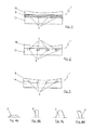
- FIG. 4 For the design of the cross sections of the tracks 3, there are various possibilities, some of which FIG. 4 are shown. Etched or vapor-deposited conductor tracks 3 are usually flat, as in FIG. 4a shown. In order to reduce the optically effective cross section but can be selected for a given resistance value, a profile of the conductor 3, in which the conductor 3 is higher than wide; this case is in FIG. 4b shown. For the cases in which the beam path at the relevant point of the optical element 1 is divergent, can also as in Fig. 4c sketched a trapezoidal cross-section of the conductor tracks 3 are selected.
- the profile of the conductor tracks 3 can be formed inclined towards the center of the optical element 1, as in FIG. 4d shown.
- the electrical conductor tracks can have a cross section of at most 1 or between 0.5 and 0.01 micrometers at least in sections laterally to the direction of incidence of the optical radiation.
- the spacing of the tracks is between 0.01 and 1 millimeters. There are also complaints between 0.05 and 0.5 millimeters possible, or specifically of 0.1 millimeters.
- FIG. 5 shows in the subfigures 5a and 5b cases in which areas of large thermal power densities are mapped.
- the case of the FIG. 5a a heat load applied in the drawing plane as vertical, not shown, caused by a dipole, in the case of use of the optical element 1 in a microlithographic projection exposure apparatus.
- the printed conductors 3 are concentrated in the in FIG. 5a illustrated case on the complementary to the area acted upon by the optical radiation area. As a result, an at least partial homogenization of the total heat input is achieved.
- Also shown in FIG. 5a are the connecting wires 7, with which the conductor elements 3 arranged in the optical element 1 are contacted.
- the optical element 1 shows a variant for a near-field position of the optical element with a formation of the heating zone corresponding to the field in the form of the scanner slot.
- the optical element 1 is in this case arranged in a field-near region of the projection lens.
- the interconnects 3 and the connecting wires 7 are shown in the optical element 1.
- the density of the heating of the optical element 1 can be varied by the spacing of the strip conductors 3 or their use, as in FIG Figure 5a and Figure 5b shown, is varied.
- the use may be a lateral variation in the sense of a lateral zigzag course of the printed conductors 3; Moreover, it is also conceivable, the use three-dimensional, for example in the manner of a coil spring form.
- FIG. 5a Another variant of the invention takes in FIG. 5a respectively.
- FIG. 5b an equal azimuthal orientation of the heat input of the optical radiation and the heat input of the conductor tracks.
- the substrate of the optical element provided with the tracks has an inverse sign of dn / dT as the optical element or elements that substantially absorb the heat input caused by the optical radiation.
- Possible pairings here are quartz glass and CaF2 or vice versa.
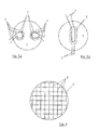
- FIG. 6 shows an optical element 1 in plan view, on which the conductor tracks 3 are arranged in the manner of a matrix.
- the horizontal and the vertical tracks are connected via not shown here heating resistors or uses.
- the possibility is created by each separate contacting of the interconnects 3 to heat locally at the intersections of the interconnects 3.
- arrangement of the tracks opens up the possibility of strip-shaped variations in the nature of the material used for the optical element, as they can occur at individual manufacturers compensate.
- an offset of the conductor tracks in the direction out of the plane of the drawing is necessary in order to be able to individually control all points of intersection.
- a coupling of individual printed conductors can also be advantageous.
- the voltage applied to the individual tracks can additionally be pulsed.
- FIG. 7 also shows in the plan view the case that the interconnects 3 are arranged in the matrix structure over the optical element 1 is not equidistant.
- the individual interconnects are connected via here again not shown heating resistors or uses.
- This embodiment of the invention is particularly useful for compensating the effects of quadrupole illumination settings in the case of using the optical element 1 in a projection exposure apparatus suitable for semiconductor lithography.
- relative geometric position of the heat inputs by the optical radiation and the heating wires or heating resistors to each other analogous statements apply as in the above-mentioned dipole lighting.
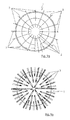
- the arrangement of the tracks or the thermal actuators have an at least approximately rotational symmetry about the optical axis, the balance of the symmetry (rotation by 360 ° / mecanicbericht transferred the arrangement in itself) 2 or higher;
- FIG. 8 shows such possibility in plan view, which is particularly suitable for the compensation of Learnwellmaschineen.
- the individual interconnects are connected via heating resistors or uses not shown here.
- the conductor tracks 3 are arranged radially star-shaped in the optical element 1; a variant in which the interconnects 3 are realized as a rotationally symmetric grid, is in FIG. 9a shown in plan view.
- the individual interconnects are connected via heating resistors, not shown here.
- heating resistors not shown here.
- FIG. 9b Another rotationally symmetric variant shows FIG. 9b in the plan view.
- no further heating resistors are provided.
- the locally different heat input is accomplished by the locally different density of the tracks. This allows a spatially high-resolution temperature control in the optical element. 1
- FIG. 10 shows the embodiments shown above only in plan view in detail at a crossing point of the conductor tracks.
- the interconnects 3a and 3b are connected in their crossing point via a resistor 8.
- it may also be a diode, a Zener diode, or a combination of a resistor, a diode and a Zener diode.
- the resistor 8 is selectively heated at the intersection of the interconnects 3a and 3b.
- the resistance is not limited to the crossing point but arranged meandering.
- the heating along the conductor tracks 3a and 3b can be kept low, that their resistance is kept small against that of the resistor 8. It is possible to arrange the interconnects 3 equidistant or not equidistant. In the case of the separate contacting of the conductor tracks 3a and 3b, respectively, it is possible to subject the conductor tracks 3a and 3b separately to voltage pulses. In this way, can be adjusted to a certain extent, the heating power in the resistor 8 and along the conductor 3a and 3b for themselves. This creates the possibility of correcting punctual errors via the resistor 8 and linearly extended errors with the conductor 3a or 3b. In FIG. 10 merely the two interconnects 3a and 3b are shown by way of example.
- a plurality of interconnects 3 may be arranged on this. If, for reasons of symmetry, for example mirror symmetry or point symmetry or rotational symmetry with respect to an azimuth such as 180 °, 90 ° or 45 °, the exposure of the optical radiation to the optical element can be waived for degrees of freedom in the correction, this has the consequence that Even individual interconnects can be short-circuited to each other, which has a simplification of the production of the optical element 1 result.
- FIG. 11 shows a variant in which the in FIG. 10 illustrated embodiment with the thoughts of FIG. 2 combined.
- a set of printed conductors 3a is buried in recesses 5 in the substrate 1a.
- the other set of printed conductors 3b is disposed on a surface of the second substrate 1b.
- the upper set of printed conductors 3b in the second substrate 1b are likewise arranged buried parallel to the drawing plane, so that it is possible to dispense with a cementing of the two substrates.
- An alternative to this is to provide a cement layer (not shown); In this case, it is possible to dispense with burying the printed conductors 3a or 3b in their respective substrates 1a and 1b.
- FIG. 12 shows a variant of the invention, in which the in FIG. 10 shown procedure is applied to the surface of an optical element 1.
- the interconnects 3a are arranged on the surface of the optical element 1 itself, which are covered by the resistive layer 9 in the region of the crossing points with the second set of interconnects 3b extending above.
- the arrangement is covered by the optical layer 6 as an antireflection layer.
- An alternative is to connect the two interconnects 3a and 3b, respectively, by a further interconnect of smaller cross-section. This must be like in FIGS. 11 and 12 shown proceed with the difference that instead of the resistive layer 9, an insulating layer is necessary.
- the further conductor track can thereby be produced by breaking the insulation layer locally by spot welding, laser welding, flashover or a lithographic production process is, resulting in the intersection points, a region between the interconnects 3a and 3b, which has a finite, but much higher resistance than the track resistance of the interconnects.
- FIG. 13 shows an optical element 1, in which conductor tracks 3 are arranged on both sides and in the inner region.
- the conductor tracks 3 may be formed flat or adapted to the incident wavefront.
- the possibility is created, for example by heating, to influence the density of the material of the optical element 1 and thus the refractive index three-dimensionally. This allows the correction of homogeneity or voltage errors even with optical elements 1, which are irradiated at large angles.
- FIG. 14 different variants are shown how the matrix structure of the tracks 3 can be made locally variable, whereby the optical effect of the tracks 3 distributed over a larger angular space.
- the density of the interconnects 3 can be varied or a different degrees of use of the interconnects 3 in frequency and amplitude can be varied to optimally adapt the local Schumansêtn to the requirements.
- the shape of the use of the conductor tracks 3 can be selected, for example, sinusoidal or sawtooth, triangular or along other functions. Of course, it is also possible to vary the profile of the conductor tracks 3.
- FIG. 15 shows a variant in which can be dispensed with resistors or a resistor or insulating layer.
- the conductor tracks 3a and 3b are formed in the vicinity of their crossing points with a reduced cross-section.
- the crossing point itself is realized in a conductive manner; This can be achieved, for example, by vapor deposition on top of each other or spot welding.
- the desired structure may be made by forming a metallization layer applied flat, z. B. is evaporated, from the below, for example, by an etching process, the structure is generated.
- an equally thick conductor track can be applied in the entire area of the optical element 1, which is varied only in its width.
- the tapers 17 and 18 of the current-carrying interconnects 3a and 3b heat up equally strong.
- a selectivity can be achieved in that not at the same time each of the interconnects 3a and 3b are placed on a voltage, but in each case only one end of the interconnects 3a and 3b.
- a voltage between the points 10 and 11 is applied in a first pulse and a voltage between the points 12 and 13 in a second pulse.
- a current flows in the direction indicated by the arrow 15, during the second pulse in the direction of the arrow 16.
- twice the power is released at the intersection point 19 as at the tapers 17 and 18th
- One possible problem with the present invention is that of crosstalk between individual interconnects. This problem becomes particularly relevant when the area coverage considered in a plan view in the optical element becomes very large.
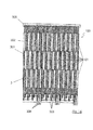
- Fig. 16 Based on Fig. 16 is explained below a way to realize a 2-dimensional array of individually controllable heating zones 101, the very high demands on the maximum area coverage, so the proportion of the surface of the optical element 1, which is covered by the tracks 3, the homogeneity of Area coverage, the homogeneity of the temperature distribution and the mutual crosstalk, so the release of undesirable heating power in a non-driven heating zone 101, is sufficient.
- the resulting scattered light component in the field is proportional to the area coverage in a first approximation.
- Typical stray light levels of modern lenses of well below one percent allow only a maximum area coverage of a few per thousand.
- the area coverage is as homogeneous as possible.
- the light intensities in this pupil plane are locally different, and relatively strongly focused, especially in dipole illumination settings. For example, one chooses an area coverage of the heating elements, which has the same effect on all diffraction orders.
- the area coverage, averaged over the typical size of a dipole spot, must be homogeneous within a few percent over the entire optically free area, that is to say over the entire area penetrated by the useful optical radiation.
- the interconnects 3 Since the interconnects 3 a local heat input into the material of in FIG. 16 cause not shown optical element 1, forms on the surface of a so-called temperature ripple, so a variation of the local temperature, from.
- the penetration depth of this temperature ripple into the optical element 1 corresponds approximately to the spacing of the interconnects 3.
- the distance between the interconnects In order to keep the influence of the temperature ripple on the optical wavefront small, the distance between the interconnects must therefore be sufficiently tight. For the same reason, it is advantageous to arrange the conductor tracks 3 as regularly as possible.
- the described problem is inventively, as in Fig. 16 by way of example on a heating field 100 with 3x3 heating zones 101 illustrated, by forming the conductor tracks 3 as an alternating arrangement of sections of lead wires 301 and heating wires 302.
- the lead wires 301 are chosen low impedance, in order to cause the lowest possible heat input in the run non-driven heating zones 101.
- the heating wires 302, however, are, for example, as in FIG. 16 represented by a cross-section reduction high impedance selected to produce the desired heat output locally in the associated heating zone 101 and in the in FIG. 16 not shown optical element 1 initiate.
- the individual, as shown in sections as supply wires 301 and heating wires 302 formed sections of the conductors 3 are electrically contacted in each case for a heating zone 101 via a bridge 303, which in turn can be connected via a connection pad 304 with a voltage source, not shown.
- a connection pad 304 with a voltage source, not shown.
- the common busbar 305 On the opposite side of the contacting of the interconnects 3 by means of the common busbar 305, which can be used for all interconnects 3 together.
- the resistance of the lead wire 301 or the feed track 301 in relation to the resistance of the heating wire 302 is chosen to be as small as possible in order to minimize undesired heating of the area through which the lead wires 301 pass.
- a much lower heating in the region of the lead wires 301 is limited to the one after the other in the direction of the tracks 3 heating zones 101 and homogeneous within the heating zones 101. This makes it possible to decouple the parasitic heat power component by a decoupling transformation on the control side; in other words, by suitable regulation on the basis of the knowledge of the activation of the desired heating zones 101, the parasitic effects in the heating zones 101 of the same heating zones arranged one behind the other can be compensated.
- the maximum, parasitic proportion of heating power within a heating zone 101 should not be greater than 10% -20% of the desired heating power.
- the parasitic heating power proportion is proportional to the number of heating zones 101 within a column minus one and the supply resistance and the heating resistance along a heating zone 101.
- the resistance of lead wires 301 and heating wires 302 can be adjusted across the line width, the layer thickness, the material choice, and the effective line length.
- Such optical elements according to the invention have 100 to 225 heating zones.
- an operating voltage of less than or equal to 200V the electronic and connection components can be realized compactly. Higher operating voltages are conceivable, but require an increasingly higher effort to avoid electrical flashovers and to ensure the dielectric strength of the electronic components.
- the minimum possible lead resistance is limited by the maximum allowable wire cross-section, which in turn is limited by the allowable area coverage and by the resistivity of suitable conductive materials. Pure elements have the lowest possible specific resistances, the resistances of alloys are generally higher than those of the elements. For a given length of heating zones 101 and a given cross-sectional boundary, the minimum possible resistance is limited by the resistivities of available conductive materials. Suitable materials for the lead wires 301 are, for example, metals having a low specific resistance, such as Ag, Cu, Au, Al, Wo, Mo, Sn or Ni.
- the lowest possible lead resistance is desirable.
- Higher resistances of the heating wires 302 can be achieved by reduced cross sections of the heating wires 302 relative to the cross sections of the lead wires 301.
- the effective length of the heating wire 302 may be extended by a meandering configuration, thereby increasing the total resistance of the heating wire 302. Over the effective length, the heating wire resistances can theoretically be arbitrarily increased, which, however, is at the expense of the area coverage, which is why length factors between 1-50 are preferred.
- a second conductor material the resistivity of which is greater than that of the lead wires 301, can be selected for the heating wires 302 in the zones 101 to be heated.
- materials for the heating wires 302 for example, higher resistivity metals such as Ni, Pt or Cr or semiconductors such as Si or Ge may be selected.
- the resistivities of the materials used are optimally adapted by doping with foreign elements for the requirements.
- the resistivity can be artificially increased by doping or by introducing alloying components, in the case of semiconductors the resistivity can be artificially reduced by the introduction of doping elements.
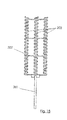
- FIG Fig. 17 An embodiment of the lead wire 301, a meandering heating wire 302 and the transition region 306 between the individual sections is shown in FIG Fig. 17 shown.
- the course of the heating wires 302 is at least in sections rounded by radii.
- bevels can be provided. Furthermore, in the transition region 306 of the two materials, a transition zone with a larger overlap area is to be provided in order to reduce the current densities in this area and thus to eliminate the risk of electrochemical degradation at the boundary layer.
- the increased overlap area defuses the overlay requirements if lead wires 301 and heater wires 302 are patterned in two separate lithography processes.
- heating wires 302 are required to have very thin lines with the lowest possible layer thicknesses in order to set the electrical resistance to the desired level, there is an increased risk of defects due to constrictions, material thinning, layer defects, resist defects, particles and stitching defects. errors.
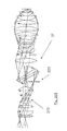
- a robust arrangement relative to such local defects is in FIG. 18 shown. Instead of a single meander now several meandering sections of the heating wire 302 are arranged in parallel and connected at regular intervals with bypasses 307 transversely. If a local defect occurs in one of the sections, the current circumscribes this point via the bypasses 307 and the adjacent meandering sections.
- the bridges 303 are realized with the aid of a second layer with conductor structures, which is electrically insulated by a suitable dielectric with respect to the first layer with the conductor tracks 3.
- a suitable dielectric with respect to the first layer with the conductor tracks 3.
- the bridges 303 are realized by bonding wires, whereby the structuring of a second layer can be saved.
- the bridges 303 are realized in the connection board.
- the number of contact points in this case corresponds to the number of printed conductors 3, the number of lines led out is reduced to the number of heating zones 101.
- the number of lead-out lines corresponding to the number of heating zones or heating wires is typically one hundred to several thousand.
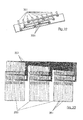
- the electrical connection is accomplished by wire-bonding on a transfer board, wherein the transfer board is mechanically decoupled from the optical element 101. Because the bonding wires are chosen very thin and the arcuate geometry is beneficial in minimizing mechanical stiffness, bonding bridges provide electrical connections with minimal mechanical rigidity and thus optimal mechanical decoupling.
- flexible conductor foils 350 for electrical connection can also be used, as in FIG Fig. 20 shown.
- all of a heating zone 101 to parent lead wires 301 can be arranged one behind the other in alignment on the same contacting track 351 on the flexible conductor foil, thereby reducing the Kunststofftechniksaufwand reduced.
- the contact pads associated with a row can be arranged on the same conductor foil 350.
- an S-shape or plural waves similar to a bellows may be impressed.
- the flexible conductor foil 350 is slotted into sections along the contacting row in order to avoid that over the surface stiffness of the flexible conductor foil 350 shearing stresses are built up, which may result in a deformation of the optical element.
- Suitable electrical contacting methods of the flexible conductor foil 350 at the contact points of the optical elements according to the invention are electrically conductive adhesive, anisotropically conductive adhesive or adhesive tapes, anisotropically conductive tapes, solder joints by stamp soldering, furnace brazing, hot air soldering or laser brazing and wire bonding.
- the conductor tracks on the optical element can be embedded in a Si0 2 layer or layer of another optically transparent dielectric.
- a Si0 2 layer or layer of another optically transparent dielectric covers any surface defects and roughness caused by the patterning process and can be overpolished to achieve the required surface accuracy of the optical element.
- An additionally occurring problem of the invention is the scattered light generated by the conductor tracks with an increasing area coverage of the conductor tracks.
- the following embodiments of the invention are formulated for projection objectives for microlithography. But they are also conceivable for other optical systems.
- the scattered light component which is caused by the interconnects in the wafer plane of a projection exposure apparatus, can be dependent not only on the areal coverage but also on the orientation of the interconnects relative to the scan direction.
- a field stop in a field position following the optical element according to the invention can be a considerable part of the field Intercept scattered light caused by the tracks, so that this does not fall on the wafer to be exposed.
- a favorable shape of the field stop corresponds to the image of the object field, in particular of the scanner field.
- the scanner slit in the scanning direction is significantly narrower than perpendicular to it, it is possible to arrange the wires perpendicular to the scanning direction, so that the stray light is diffracted in the scanning direction, whereby a significantly larger part is intercepted by the narrower in this direction field aperture than perpendicular to it.
- the field is larger orthogonal to the scan direction than in the scan direction.
- this "short" direction of the field it is easier to catch stray light than perpendicular to it. Stray light by straight conductor tracks, which are oriented perpendicular to the scanning direction, can therefore be more easily intercepted and thus reduced.
- a variant of the invention consists in the fact that the optical element according to the invention is positioned in or near a pupil plane, while the Falllblende is designed closer to the field and at least partially mounted in the direction of the short field direction laterally next to the Nutzstrahlengang.
- the use of at least one aperture diaphragm, which is arranged in the light direction after the optical element according to the invention, is an effective way to suppress stray light.
- optical elements for other reasons can be divided into different individual elements and offer themselves through this distribution anyway required as a carrier of correction means such as conductor tracks or thermal actuators.
- the use of crystalline optic materials such as calcium fluoride, barium fluoride, barium lithium fluoride, other fluorides, LuAG (luthetium aluminum garnet) or spinel, which show intrinsic birefringence in the ultraviolet range, is conceivable for the realization of the optical element according to the invention.
- LuAG lathetium aluminum garnet
- spinel which show intrinsic birefringence in the ultraviolet range
- the main crystallographic axes may be oriented in the [100], [111] or [110] direction in the direction of the optical axis of the system, the corresponding compensation schemes are widely found in the literature.
- a calibration data record in advance for the optical element according to the invention.
- one controls the individual local areas with a defined current intensity and measures interferometrically the resulting influence on the wavefront. Based on this information, the local areas are later controlled so that a highly accurate optical effect of the local temperature changes is achieved.
- the optical element according to the invention can be designed as a replacement part.
- the correction means according to the invention may be adapted to the preferred use of the projection exposure apparatus, i. for example, to dipole or quadrupole illumination.
- the replacement parts may have different aspheric effect by different surface shapes or be designed to correct specific changes in the projection lens by, for example, Compaction.
- the optical element is designed as a plane-parallel plate, it may be useful to make it displaceable in a divergent or convergent beam path along the optical axis. Due to a shift along the optical axis, the subaperture ratios then change appreciably due to the divergent beam path, so that the optical element can operate in each case for the optimum system state. Such a shift may be useful if, for example, lifespan and lens heating effects are dominant in different subaperture areas and interfere with different weights depending on the usage and duration that the system is already in use.
- the optical element can additionally be variable in its position (decentration, tilt preferably about an axis parallel or perpendicular to the optical axis, rotation) and / or in particular astigmatic, three- or four-wave deformable (within the load limits of the conductors or thermal actuators ) be designed.
- the said displacements / rotations / tiltings of the optical element can of course also be provided if the optical element is located in a non-divergent or convergent part of the beam path.
- a first mode e.g. generates a low wavefront error with uniform lens warming, but sensitive to false light
- a second mode of operation generates strong heating effects, but it may be useful to provide a quick exchange of the optical element according to the invention against an optical element which is unstructured and the same desired optical effect as the non-driven inventive optical element has.
- the first mode of operation the unstructured optical element which does not generate a false light is used in the beam path.
- the optical element according to the invention is used and the wavefront error caused by the, for example, uneven heating of the second mode is corrected by the element.
- the optical element according to the invention is designed in such a way that it can be exchanged during operation of the projection exposure apparatus, that is, in particular held in a mechanical exchange fit and precautions are taken for easy accessibility.
- the fault to be corrected must be known as accurately as possible.
- this information can be obtained from measurements of the wavefront error on projection exposure apparatuses during operation.
- the irradiation is constant in the conducting agent, it is possible to extrapolate to the amount of absorbed light and the temperature distribution which results. From this, the temporally developing aberrations can be calculated and used as a basis for a correction. The extrapolations can either be based on simultaneous high-speed simulations or based on them previous calibrations based on a measurement of the wavefront error.
- measurements should then preferably be performed at shorter intervals if the irradiation changes, for example immediately after a change of the reticle and / or illumination has taken place.
- the time evolution will be particularly rapid, so that in the first case, the frequency of the system measurements at the time interval to the last change in irradiation and the (previously known by calculation or measurement) system time constants can be adjusted. If the system approaches the static state ("saturation"), it will be necessary to measure less frequently, and the throughput of exposed projection imaging system wafers will increase accordingly.
- paraxial subaperture ratio serves as a measure of the position in the system.
- a definition of the paraxial Edge beam or paraxial main beam is in " Fundamental Optical Design "by Michael J. Kidger, SPIE PRESS, Bellingham, Washington, USA given by reference herein.
- the paraxial subaperture ratio is a signed quantity, which is a measure of the field or pupil near a plane in the beam path.
- the subaperture ratio is normalized to values between -1 and 1, where each field plane corresponds to a zero of the paraxial subaperture ratio, and where each pupil plane corresponds to a discontinuity with a jump of the paraxial subaperture ratio from -1 to +1 or from +1 to -1 ,
- paraxial subaperture ratios of 0 for the present application designate field levels, while a magnitude paraxial subaperture ratio of 1 determines a pupil level.
- Near-field levels thus have paraxial subaperture ratios that are close to 0, while near-pupal levels have paraxial subaperture ratios that are close to 1 in magnitude.
- the sign of the paraxial sub-pair ratio indicates the position of the plane in front of or behind a reference plane. For definition, e.g. the sign of the piercing point of a Komastrahls be used in the area concerned.
- Two planes in the beam path are called conjugate if they have the same paraxial subaperture ratio.
- Pupillary planes are conjugated to each other, as well as field levels.
- the optical elements or the arrangement according to the invention can be arranged at a location in the system at which the paraxial subaperture ratio for a first element according to the invention or for a first arrangement according to the invention is greater than 0.8, preferably greater than 0.9.
- an inventive optical element, or an inventive arrangement be present for for which the paraxial subaperture ratio is less than 0.9, preferably less than 0.8.
- a further optical element according to the invention or a further arrangement according to the invention may be present whose subaperture ratio is smaller than 0.8 in absolute value and whose subaperture ratio has the opposite sign to that of the second element or to that of the second arrangement.
- the respective paraxial subaperture ratios differ by at least 0.15, preferably 0.3, from one another.
- the dioptric projection lens 37 in FIG Figure 201 which also in the WO 2003/075096 A2 is shown, which is hereby fully integrated into this application, there is an optical element 211, which is designed as a flat plate.
- This plane plate is designed to be interchangeable. In one embodiment of the invention of the optical element 211, this is equipped with the conductor tracks according to the invention and can be exchangeable and / or not exchangeable.
- This plane plate is located at a position corresponding to a subaperture ratio between 0.9 and 1.0.
- the projection objective 37 according to the invention can be provided with a scattered light diaphragm 221 between the last optical element in the direction of the beam path and the wafer, not shown here.
- an optical element 212 which is designed as a plane plate.
- the optical element 212 according to the invention is equipped with the strip conductors according to the invention and can be exchangeable and / or not exchangeable.
- This plane plate is located at a position corresponding to a subaperture ratio between -0.8 and -0.9. Therefore This plan plate is a little closer to the field than in the previous embodiment.
- the projection objective 37 according to the invention can be provided with a scattered-light diaphragm 222 in a pupil plane of the projection objective 37.
- the projection objective 37 according to the invention can be provided with a scattered-light diaphragm 223 in the vicinity of an intermediate image.
- the scattered light aperture can have the image of the scanner slot in the intermediate image plane.
- the invention can be used in catoptric projection lenses for microlithography.
- One way to avoid moiré effects is to arrange the optical elements according to the invention azimuthally folded with respect to the orientation of their interconnects. For example, you can entangle by 90 °.
- stray-light advantageous orientation of the interconnects orthogonal to the scanning direction of the projection exposure system, as in FIG. 21 shown only a slight, in particular less than 5 °, azimuthal entanglement of the interconnects of the respective optical elements according to the invention made against each other.
- Such an entanglement can be carried out relative to several individual optical elements according to the invention. But it can also be made within a single optical element according to the invention.
- FIG. 204 is a projection exposure apparatus 31 for semiconductor lithography, in which the described optical elements according to the invention are integrated, shown. This is used to illuminate structures on a coated with photosensitive materials substrate, which generally consists predominantly of silicon and is referred to as wafer 32, for the production of semiconductor devices, such as computer chips.
- the projection exposure apparatus 31 consists essentially of a lighting device 33, a device 34 for receiving and exact positioning of a mask provided with a structure, a so-called reticle 35, by which the later structures on the wafer 32 are determined, a device 36 for mounting, Movement and exact positioning of just this wafer 32 and an imaging device, namely a projection lens 37, with a plurality of optical elements 38, which are mounted on sockets 39 in a lens housing 40 of the projection lens 37.
- an inventive optical element 1 at any point in
- the basic functional principle provides that the structures introduced into the reticle 35 are imaged onto the wafer 32; the image is usually scaled down.
- the wafer 32 After exposure has taken place, the wafer 32 is moved further in the direction of the arrow so that a multiplicity of individual fields, in each case with the structure predetermined by the reticle 35, are exposed on the same wafer 32.
- the exposure process itself can be carried out during a relative rest position of the wafer and the reticle relative to one another (wafer stepper) or during a relative movement of the wafer and reticle (wafer scanner).
- the illumination device 33 provides a projection beam 41 required for imaging the reticle 35 on the wafer 32, for example light or similar electromagnetic radiation.
- the source of this radiation may be a laser or the like.
- the radiation is formed in the illumination device 33 via optical elements in such a way that the projection beam 41 has the desired properties when it strikes the reticle 35: polarization, homogeneous field illumination ("uniformity") or intensity profile, telecentricity, shadowing at the edge of the field, application-specific pupil filling ( Dipole, quadrupole, annular) with requirements for symmetry.
- the projection lens 37 has a plurality of individual refractive, diffractive and / or reflective optical elements 38, such as lenses, mirrors, prisms, end plates and the like on.
Abstract
Description
Die vorliegende Erfindung betrifft ein optisches Element und ein Verfahren zur Beeinflussung des optischen Verhaltens dieses optischen Elements, sowie die Verwendung des optischen Elements in einem optischen System, vorzugsweise in einer Projektionsbelichtungsanlage für die Mikrolithographie. Ferner betrifft die vorliegende Erfindung eine Projektionsbelichtungsanlage bzw, ein Projektionsobjektiv für die Mikrolithographie, welche bzw. welches das erfindungsgemäße optische Element enthält. Ferner betrifft die vorliegende Erfindung ein Verfahren zum Betrieb dieser erfindungsgemäßen Projektionsbelichtungsanlage bzw. dieses erfindungsgemäßen Projektionsobjektivs.The present invention relates to an optical element and a method for influencing the optical behavior of this optical element, and to the use of the optical element in an optical system, preferably in a projection exposure apparatus for microlithography. Furthermore, the present invention relates to a projection exposure apparatus or a projection objective for microlithography, which contains the optical element according to the invention. Furthermore, the present invention relates to a method for operating this projection exposure apparatus according to the invention or this projection objective according to the invention.
In modernen Projektionsobjektiven für die Mikrolithographie wird eine Vielzahl von Wellenfront-Manipulatoren zur Korrektur von optischen Aberrationen eingesetzt. Die meisten dieser Manipulatoren bewirken eine Wellenfront-Korrektur über mechanische Manipulation von optischen Elementen. Dies geschieht entweder über eine Positionsänderung und/oder über eine Deformation der optischen Elemente. Diese Manipulatoren haben Korrekturmöglichkeiten für niederwellige Wellenfrontfehler wie sie typischerweise bei der Verwendung der Objektive in Verbindung mit sogenannten konventionellen Settings und bei einem Durchsatz von etwa 120 Wafer/Stunde auftreten.Modern projection objectives for microlithography use a variety of wavefront manipulators to correct optical aberrations. Most of these manipulators cause wavefront correction via mechanical manipulation of optical elements. This is done either via a change in position and / or via a deformation of the optical elements. These manipulators have low-wavefront error correction capabilities typically encountered with the use of the lenses in conjunction with so-called conventional settings and at a throughput of about 120 wafers / hour.
Stetig steigende Durchsatz-Anforderungen bedingen jedoch immer höhere Lichtintensitäten im Objektiv und damit eine stetig steigende Thermallast, die auf die optischen Elemente wirkt. Diese Thermallast verursacht Wellenfront-Fehler: bei Linsen über den temperaturabhängigen Brechungsindex und die Oberflächendeformation, bei Spiegeln vorwiegend durch die Oberflächendeformation aufgrund der thermischen Ausdehnung des Spiegelsubstrates. Hinzu kommt in der Entwicklung der Lithographie der Trend zu Beleuchtungs-Settings, wie zum Beispiel den Dipol-Settings, die eine starke Fokussierung der Lichtleistungsdichte auf insbesondere pupillennahen Linsen mit sich bringen und damit, aufgrund der hieraus resultierenden lokal hohen Thermallast, auch radiale und/oder azimutale höherwellige und stark lokalisierte Wellenfrontfehler verursachen können. Diese können mit den eingangs erwähnten Manipulatoren nur noch bedingt kompensiert werden. Das gleiche gilt für Wellenfrontfehler, die durch lichtinduzierte Lebensdauereffekte wie Compaction, welche aufgrund der höheren optischen Leistungsdichten verstärkt hervortritt, verursacht werden. Auch diese Wellenfrontfehler können mit den bisher bekannten Manipulatoren nicht effizient kompensiert werden.Constantly increasing throughput requirements, however, require ever higher light intensities in the lens and thus a steadily increasing thermal load, which acts on the optical elements. This thermal load causes wavefront errors: in the case of lenses over the temperature-dependent refractive index and the surface deformation, in mirrors predominantly by the surface deformation due to the thermal expansion of the mirror substrate. in addition In the development of lithography, the trend is towards lighting settings, such as the dipole settings, which bring about a strong focusing of the light power density on, in particular, near-pupil lenses and thus, due to the resulting locally high thermal load, also radial and / or azimuthal higher-wave and strongly localized wavefront errors can cause. These can be only partially compensated with the manipulators mentioned above. The same is true for wavefront errors caused by light-induced lifetime effects such as compaction, which is more pronounced due to the higher optical power densities. These wavefront errors can not be compensated efficiently with the previously known manipulators.
Eine Möglichkeit, diese durch Lebensdauereffekte verursachten Wellenfrontfehler in effizienterer Weise zu kompensieren, ist derzeit die Verwendung von tauschbaren Platten, auf die spezielle Korrekturasphären aufgebracht sind. Innerhalb der Lebensdauer des Objektivs müssen diese Kompensationsplatten mehrmals getauscht werden, um den Änderungen der Wellenfrontfehler während der Lebensdauer des Objektivs angemessen gerecht zu werden.One way to more efficiently compensate for these wavefront errors caused by lifetime effects is currently the use of exchangeable plates with special correction aspheres applied to them. Over the lifetime of the lens, these compensation plates must be replaced several times to adequately accommodate the changes in wavefront error over the life of the lens.
Kompensationsplatten mit Korrekturasphären können zwar Fehler kompensieren, sie sind aber zur Kompensation dynamisch schnell veränderlicher Fehler eher ungeeignet. Auch muss der zu kompensierende Fehler vor der Erstellung der Kompensationsplatte und insbesondere damit vor ihrem Einbau in das Projektionsobjektiv bekannt sein. Da mit dem Einbau der Kompensationsplatte wiederum neue Wellenfrontfehler induziert werden, ist hier naturgemäß keine vollständige Kompensation möglich.Although compensation spheres with correction aspheres can compensate for errors, they are rather unsuitable for compensating dynamically rapidly changing errors. Also, the error to be compensated must be known prior to the preparation of the compensation plate and in particular before its installation in the projection lens. As new wavefront errors are again induced with the installation of the compensation plate, complete compensation is naturally not possible here.
Die zu lösende Problemstellung besteht nun darin, einen Wellenfront-Manipulator zu finden, mit dem möglichst flexibel Wellenfrontfehler, synonym Aberrationen, und hierbei insbesondere radial und/oder azimutal höherwellige Aberrationen, kompensiert werden können. Eine ideale Lösung dieses Problems besteht aus steuerbaren, 2-dimensionalen Korrekturasphären, welche insbesondere die radial und/oder azimutal höherwellige Aberrationen kompensieren.The problem to be solved is now to find a wavefront manipulator, with the most flexible wavefront error, synonymous aberrations, and in this case in particular radially and / or azimuthally higher-wave aberrations, can be compensated. An ideal solution to this problem consists of controllable, 2-dimensional correction spheres, which in particular compensate the radially and / or azimuthally higher-wave aberrations.
Wie bereits erwähnt sind etablierte Manipulatoren im obigen Sinne insbesondere mechanischer Art. So beschreibt beispielsweise die
Aus
Da mechanische Elemente im optischen Strahlengang jedoch Abschattung und Streulicht verursachen, sind, im Falle von zu manipulierenden Linsen, mechanische Konzepte auf die Manipulation des Linsenrandes beschränkt. Diese Beschränkung auf den Linsenrand stellt eine inhärente Einschränkung der möglichen Korrekturprofile und speziell der radialen Ordnungen dar, die sich auch durch aufwendige Mechanismen nicht umgehen lässt.However, since mechanical elements in the optical beam path cause shading and stray light, in the case of lenses to be manipulated, mechanical concepts are limited to the manipulation of the lens edge. This limitation to the lens edge is an inherent limitation of the possible correction profiles and especially of the radial orders, which can not be circumvented even by complicated mechanisms.
Alternativ zu den mechanischen Manipulatoren sind thermische Manipulatoren bekannt, wobei die thermischen Manipulatoren ebenfalls am Linsenrand angeordnet sind wie beispielsweise in der US-Patentschrift
Ferner ist ein Verfahren zur Korrektur nicht rotationssymmetrischer Bildfehler mit am Umfang von Linsen angeordneten Peltier-Elementen aus der
Eine Vorrichtung und ein Verfahren zur Korrektur asymmetrischer Temperaturbelastungen eines optischen Elements wie einer Linse oder eines Spiegels sind ebenfalls aus der
Aus der
Ferner ist aus der
Die Schriften
Die Aufgabe der vorliegenden Erfindung ist es, ein alternatives Verfahren zur Korrektur von Projektionsbelichtungsanlagen für die Mikrolithographie hinsichtlich ihrer Abbildungsfehler bereitzustellen, wobei insbesondere zeitlich veränderliche Abbildungsfehler und / oder azimutal und / oder radial höherwellige Abbildungsfehler als relevant erachtet sind. Eine weitere Aufgabe der vorliegenden Erfindung ist es, ein optisches Element sowie ein Verfahren anzugeben, das es erlaubt, eine auf das optische Element einfallende elektromagnetische Strahlung zeitlich und räumlich lokal zu beeinflussen. Ferner ist eine Aufgabe der vorliegenden Erfindung, eine Projektionsbelichtungsanlage bzw. ein Projektionsobjektiv für die Halbleiterlithographie anzugeben, welche bzw. welches hinsichtlich etwaiger Abbildungsfehler dynamisch korrigiert werden kann.The object of the present invention is to provide an alternative method for the correction of projection exposure systems for microlithography with respect to their aberrations, wherein in particular temporally variable aberrations and / or azimuthal and / or radial higher-wavefront aberrations are considered relevant. A further object of the present invention is to specify an optical element and a method which makes it possible to temporally and spatially influence an electromagnetic radiation incident on the optical element locally. A further object of the present invention is to provide a projection exposure apparatus or a projection objective for semiconductor lithography, which can be dynamically corrected for any imaging errors.
Ferner ist es die Aufgabe der Erfindung, ein Verfahren zum Betrieb einer Projektionsbelichtungsanlage bzw. eines Projektionsobjektivs für die Halbleiterlithographie anzugeben, welche eine örtlich und zeitlich stark aufgelöste Korrektur von Abbildungs- fehlern erlaubt.Furthermore, it is the object of the invention to specify a method for operating a projection exposure apparatus or a projection objective for semiconductor lithography, which permits a locally and temporally highly resolved correction of imaging errors.
Diese Aufgabe wird durch die Vorrichtungen mit den in den unabhängigen Ansprüchen aufgeführten Merkmalen gelöst. Die Unteransprüche betreffen vorteilhafte Varianten und Weiterbildungen der Erfindung.This object is achieved by the devices having the features listed in the independent claims. The subclaims relate to advantageous variants and developments of the invention.
Eine Lösung der obigen Problemstellung besteht nun darin, ein optisches Element mit einem frei einstellbaren Temperaturprofil zu realisieren. Notwendig hierzu ist die Fähigkeit, dem Element an jeder Stelle Wärme zuzuführen zu können. Die Anforderungen an die optische Performance der Projektionsobjektive bedingen jedoch sehr stringente Einschränkungen hinsichtlich der optisch wirksamen Elemente, die im Strahlengang platziert werden dürfen. Für pupillennahe Elemente ergibt sich eine maximale erlaubte homogene Flächendeckung, d.h. eine Abschattung des Stahlenganges, von grössenordnungsmässig wenigen Promille. Für feldnahe Elemente sind die Einschränkungen noch stärker. Die Verwendung von fluid-mechanischen Wärmepumpen ist damit ausgeschlossen.A solution of the above problem is now to realize an optical element with a freely adjustable temperature profile. What is needed is the ability to heat the element at any point. However, the requirements on the optical performance of the projection lenses require very stringent restrictions with regard to the optically active elements that may be placed in the beam path. For pupil-near elements results in a maximum allowed homogeneous area coverage, ie shading of the steel passage, of the order of magnitude few per thousand. For field-related elements, the restrictions are even stronger. The use of fluid-mechanical heat pumps is thus excluded.
Das erfindungsgemäße optische Element besitzt wenigstens eine elektrische Leiterbahn, wobei die optische Wirkung des optischen Elementes durch eine Ansteuerung der Leiterbahn beeinflussbar ist.The optical element according to the invention has at least one electrical conductor, wherein the optical effect of the optical element can be influenced by a control of the conductor.
Die optische Dicke des optischen Elements kann somit über die Temperaturabhängigkeit des optischen Brechungsindexes des optischen Elementes variiert werden. Die Phasenvariation Δϕ ist dabei näherungsweise proportional zum durchlaufenen erwärmten Weg im optischen Element ΔZ, der Temperatursensitivität des optischen Brechungsindexes dn/dT und der Temperaturvariation ΔT 
Für eine gegebene Geometrie des optischen Elementes ist die Phasenänderung somit näherungsweise proportional zur Temperaturänderung. Eine optische Wellenfront, die ein optisches Element durchläuft, erfährt daher eine Wellenfrontdeformation, die dem Temperaturprofil des optischen Elementes entspricht. Umgekehrt kann eine deformierte Wellenfront durch ein geeignetes inverses Temperaturprofil korrigiert werden.For a given geometry of the optical element, the phase change is thus approximately proportional to the temperature change. An optical wavefront passing through an optical element therefore experiences wavefront deformation that corresponds to the temperature profile of the optical element. Conversely, a deformed wavefront can be corrected by a suitable inverse temperature profile.
Innerhalb des sehr kleinen Temperaturbereichs von typischerweise weniger als einem Kelvin bis zu einigen Kelvin kann die Temperaturänderung des Brechungsindexes als konstant über die Temperatur angenommen werden. Für Quarzglas ergibt sich zum Beispiel eine Empfindlichkeit von etwa 0.002/1mK, mit 1K Temperaturhub kann also bei 20mm Glasdicke ein Phaseneffekt von 400nm erzeugt werden.Within the very small temperature range, typically less than one Kelvin to a few Kelvin, the temperature change of refractive index can be assumed to be constant over temperature. For quartz glass, for example, results in a sensitivity of about 0.002 / 1mK, with 1K Temperaturhub can thus be produced at 20mm glass thickness, a phase effect of 400nm.
Dies ist hinreichend zur Korrektur der typischen Amplituden von hochwelligen Wellenfrontfehlern in Projektionsobjektiven für die Mikrolithographie.This is sufficient to correct the typical amplitudes of high wavefront aberrations in microlithography projection objectives.
Zusätzlich zur Brechzahländerung wird auch die wärmebedingte Ausdehnung des optischen Elementes für die Veränderung der optischen Wirkung des optischen Elementes relevant. Diese Phasenvariation Δϕ' ist dabei örtlich lokal näherungsweise proportional zum Sprung des Brechungsindex an der Grenze des optischen Elementes Δn, der Ausdehungssensitivität bzw. des thermischen Ausdehnungskoeffizienten (CTE) des optischen Elementes dZ/dT und der Temperaturvariation ΔT 
Je nach Anordnung der Leiterbahn im optischen Element variieren dabei die Anteile der Wirkungen aus der Änderung des Brechungsindexes des optischen Elementes und der Formvariation einer optisch wirksamen Fläche des optischen Elementes, Bei Spiegeln ist naturgemäß nur Letzteres wirksam.Depending on the arrangement of the conductor track in the optical element, the proportions of the effects from the change in the refractive index of the optical element and the shape variation of an optically active surface of the optical element vary. In the case of mirrors, of course, only the latter is effective.
Wird eine Leiterbahn zur Temperierung verwendet, so ist es aufgrund der bereits geschilderten Abschattungsproblematik einerseits vorteilhaft, wenn diese mindestens abschnittsweise orthogonal zur Einfallsrichtung der optischen Strahlung einen Querschnitt von weniger als 50µm aufweist, damit die Leiterbahn an sich die optische Wirkung des optischen Elementes nicht beeinträchtigt. Andererseits ist es vorteilhaft, durch eine hinreichende Dichte der Leiterbahnen die örtlich freie Einstellbarkeit der Temperatur im optischen Element zu gewährleisten. Vorteilhaft sind Abstände zwischen den Leiterbahnen, die eine laterale Auflösung des Wellenfrontfehlers von 10 - 15 Prozent des Pupillendurchmessers gewährleisten.If a conductor track is used for tempering, it is on the one hand advantageous due to the shading problem already described, if this at least partially orthogonal to the direction of incidence of the optical radiation has a cross section of less than 50 μ m, so that the conductor does not intrinsically the optical effect of the optical element impaired. On the other hand, it is advantageous to ensure the location-free adjustability of the temperature in the optical element by a sufficient density of the conductor tracks. Distances between the interconnects are advantageous, which ensure a lateral resolution of the wavefront error of 10 to 15 percent of the pupil diameter.
In Abhängigkeit von der Position des erfindungsgemäßen optischen Elementes in dem abbildenden System, in dem es zum Einsatz kommt, können auch kleinere Ausdehnungen der Leiterbahn als 50µm von Vorteil sein. Bei einer Position im Bereich einer Pupillenebene eines Projektionsobjektives für die Halbleiterlithographie sind insbesondere Ausdehnungen von ca. 1µm äußerst vorteilhaft. Diese zusätzlich einschränkende Maßnahme hat die Wirkung, dass aufgrund des vergleichsweise geringen Durchmessers der Leiterbahn eine Beeinträchtigung der Funktionalität des optischen Elementes weitgehend vermieden oder sogar ausgeschlossen wird, und dass bei einer geeigneten räumlichen Verteilung der Leiterbahn nur ein geringer Anteil des optisch wirksamen Anteils des optischen Elementes von der Abschattung betroffen ist.Depending on the position of the optical according to the invention Elements in the imaging system in which it is used may also be advantageous for smaller dimensions of the track than 50 μm . In a position in the region of a pupil plane of a projection objective for semiconductor lithography, in particular expansions of approximately 1 μm are extremely advantageous. This additionally restrictive measure has the effect that, owing to the comparatively small diameter of the conductor track, impairment of the functionality of the optical element is largely avoided or even ruled out, and that with a suitable spatial distribution of the conductor track only a small portion of the optically effective portion of the optical element is affected by the shading.
Mit Methoden der Feinstleiterätzung aus der Leiterplattenherstellung, der Lithographie, der Elektronenstrahl Lithographie oder mit Laser-Mikrostrukturierung ist es möglich, die Leiterbahnen bis zu einer minimalen Ausdehnung von ca. 0,5 µm bis zu 10 nm herzustellen.With methods of Feinstleiterätzung from printed circuit board production, lithography, electron beam lithography or laser microstructuring, it is possible to produce the conductor tracks to a minimum extent of about 0.5 .mu.m up to 10 nm.
Um einen negativen Einfluss der Leiterbahnen an sich auf die optische Wirkung des optischen Elementes zu vermeiden ist nicht nur der Durchmesser der Leiterbahnen zu beschränken sondern auch die von den Leiterbahnen insgesamt verursachte Abschattung im optischen Element.In order to avoid a negative influence of the interconnects per se on the optical effect of the optical element is not only to limit the diameter of the interconnects but also the overall shading caused by the interconnects in the optical element.
Im Fall der Anwendung der Erfindung für in einem Projektionsobjektiv für die Halbleiterlithographie verwendete optische Elemente lässt sich die folgende Abschätzung vornehmen: abhängig von der Position des optischen Elementes im Objektiv seien beispielsweise Blasenklassen bis 5x0,25 erlaubt. Dies entspricht einer Gesamtfläche von 1,25mm2. Nach ISO 1010-3 ist es erlaubt, diese Fläche auf mehr Blasen einer äquivalenten Gesamtfläche zu verteilen, solange hierbei keine Häufung auftritt. In erster Näherung wäre es also zulässig, eine Leiterbahn mit einer Länge von bis zu 1,25m und einer Breite von 1µm auf dem optischen Element zu verteilen. Gegebenenfalls kann durch Unregelmäßigkeiten in der Verteilung oder der Breite und der Querschnittsform der Leiterbahn sichergestellt werden, dass es nicht zu systematischen Effekten wie z. B. der Beeinflussung bestimmter Beugungsordnungen oder einem gerichtetem Streulicht kommt.In the case of the application of the invention for optical elements used in a projection objective for semiconductor lithography, the following estimation can be made: depending on the position of the optical element in the objective, bubble classes up to 5x0.25, for example, are permitted. This corresponds to a total area of 1.25mm 2 . According to ISO 1010-3 it is allowed to distribute this area over more bubbles of an equivalent total area, as long as there is no accumulation. In a first approximation, it would be permissible to distribute a conductor track with a length of up to 1.25 m and a width of 1 μ m on the optical element. It may be due to irregularities be ensured in the distribution or the width and the cross-sectional shape of the conductor that it is not too systematic effects such. B. the influence of certain orders of diffraction or directed stray light comes.
Die Erfindung eignet sich insbesondere für eine Anwendung im durchstrahlten Bereich von Linsen oder Planplatten; ebenso ist aber auch eine Verwendung auf oder auch hinter der reflektiven Oberfläche eines Spiegels denkbar. Ebenso ist eine Verwendung in Strahlteilern denkbar, welches aus einem refraktiven und einem reflektiven Teil bestehen. Die durch den Wärmeeintrag induzierte optische Wirkung entspricht in allen Fällen, wo ein erster, von Licht durchtretender und ein zweiter, das Licht reflektierender Bereich des optischen Elementes auftritt, der Überlagerung der oben beschriebenen Wirkungen auf den Brechungsindex und die Formvariation des optischen Elementes.The invention is particularly suitable for use in the irradiated area of lenses or plane plates; but also a use on or behind the reflective surface of a mirror is conceivable. Likewise, a use in beam splitters is conceivable, which consist of a refractive and a reflective part. The optical action induced by the heat input corresponds to the superimposition of the above-described effects on the refractive index and the shape variation of the optical element in all cases where a first light-transmitting region and a second light-reflecting region of the optical element occur.
Durch die wenigstens eine vorzugsweise verteilt angeordnete elektrisch leitende Leiterbahn im Bereich einer optisch wirksamen optischen Fläche des erfindungsgemäßen optischen Elements lässt sich vorteilhaft über elektrische Leistung das optische Element in der Nähe der optisch wirksamen Fläche lokal erwärmen, z.B. um einige Millikelvin, so dass sich die optisch wirksame Fläche aufgrund des Wärmeeintrags hinsichtlich ihrer Form oder anderer Parameter steuerbar verändern lässt, Damit ist es möglich, die optische Wirkung des optischen Elements mittels der durch die elektrisch leitende Leiterbahn eingetragenen elektrischen Leistung zu steuern. Dies lässt sich dazu verwenden, um in einem optischen Abbildungssystem, wie z. B. einer Projektionsbelichtungsanlage, Abbildungsfehler höherer Ordnung dynamisch zu korrigieren. Durch den möglichen Einsatz des Korrekturelementes in Transmission lassen sich Abbildungsfehler höherer radialer und / oder azimutaler Ordnung an beliebigen Positionen in einem optischen Abbildungssystem korrigieren, also insbesondere auch an Positionen, an denen keine lokal deformierbaren Spiegel vorgesehen sind, beispielsweise also auch in rein refraktiven optischen Abbildungssystemen.By means of the at least one preferably electrically distributed conductor track in the region of an optically effective optical surface of the optical element according to the invention, the optical element in the vicinity of the optically active surface can advantageously be locally heated by electrical power, for example by a few millikelvin, so that the optically This makes it possible to control the optical effect of the optical element by means of the recorded by the electrically conductive trace electrical power. This can be used to in an optical imaging system, such. B. a projection exposure system to correct aberrations higher order dynamically. Due to the possible use of the correction element in transmission, aberrations of higher radial and / or azimuthal order can be corrected at arbitrary positions in an optical imaging system, ie in particular at positions where no locally deformable mirrors are provided, for example also in purely refractive optical Imaging systems.
Der Wellenlängenbereich der auf das optische Element einfallenden, elektromagnetischen Strahlung liegt vorzugsweise im optischen Bereich bis hin zum extrem ultravioletten Bereich (EUV), das heißt, in einem Spektralbereich von ca. 10 nm - ca. 1µm. Das optische Element der vorliegenden Erfindung lässt sich jedoch auch anwenden für elektromagnetische Strahlung, die den wellenlängenbereich von 1µm übersteigt wie z. B. im Infrarot- und Ferninfrarotbereich bis hin zu 10 µm.The wavelength range of the incident on the optical element, electromagnetic radiation is preferably in the optical range up to the extreme ultraviolet range (EUV), that is, in a spectral range of about 10 nm - about 1 micron. However, the optical element of the present invention can also be used for electromagnetic radiation that exceeds the wavelength range of 1 micron, such as. B. in the infrared and far infrared range up to 10 microns.
Die wenigstens eine im optischen Element vorzugsweise verteilt angeordnete, elektrisch leitende Leiterbahn kann sowohl auf einer optisch wirksamen Fläche des optischen Elementes als auch unterhalb einer optisch wirksamen Oberfläche im Inneren des optischen Elementes angeordnet sein. Die elektrisch leitende Leiterbahn des erfindungsgemäßen optischen Elements umfasst ferner Anschlusselemente zum elektrischen Ansteuern der Leiterbahn.The at least one in the optical element preferably distributed, arranged electrically conductive trace can be arranged both on an optically active surface of the optical element and below an optically active surface in the interior of the optical element. The electrically conductive track of the optical element according to the invention further comprises connection elements for electrically driving the conductor track.
Das erfindungsgemäße optische Element gestattet es, die Wellenfront der elektromagnetischen Strahlung mit einer ähnlichen Ortsauflösung wie bei der Verwendung von mittels Ion Beam Figuring hergestellte Korrekturasphären zu kontrollieren, allerdings kann die Einstellung im Unterschied zu der konventionellen Vorgehensweise dynamisch innerhalb weniger Sekunden geändert werden.The optical element according to the invention makes it possible to control the wavefront of the electromagnetic radiation with a similar spatial resolution as when using correction spheres produced by Ion Beam Figuring, but the setting can be changed dynamically within a few seconds, unlike the conventional approach.
Durch die Verwendung vorab berechneter, statischer Heizprofile kann die aufwendige Herstellung und Integration der o. g. Korrekturasphären ersetzt werden. Ebenso können verschiedene, vorprogrammierte Korrekturwirkungen dynamisch "aufgeschaltet" werden, was zur Verbesserung der Auflösung bei bestimmten Anwendungen dienen kann. Vorausberechnete, oder von Messdaten abgeleitete Korrekturprofile können dabei Abbildungsfehler aufgrund von Compaction/Rarefaction (d. h. lokale Dichteänderungen des Materials des optischen Elementes), verspannten Fassungen der optischen Elemente oder oberflächendeformationen des optischen Elementes korrigieren. Im Zusammenspiel mit Informationen aus einem Steuerrechner über den aktuellen Betriebsmodus des Systems, in dem das erfindungsgemäße optische Element eingesetzt ist, können dynamisch lokale Dichte- und Formänderungen aufgrund der Erwärmung des optischen Elementes kompensiert werden. Ferner ist auch eine automatische Rückkopplungsschleife denkbar, bei der Daten von Wellenfrontsensoren direkt zur Ableitung des benötigten Heizprofils verwendet werden.By using pre-calculated, static heating profiles, the costly production and integration of the above correction spheres can be replaced. Likewise, various pre-programmed correction effects can be dynamically "switched on", which can serve to improve the resolution in certain applications. Predicted or derived from measurement data correction profiles can thereby aberrations due to Compaction / Rarefaction (ie local density changes of the material of the optical element), straightened frames of the optical elements or surface deformations of the optical element. In interaction with information from a control computer on the current operating mode of the system in which the optical element according to the invention is used, dynamically local density and shape changes due to the heating of the optical element can be compensated. Furthermore, an automatic feedback loop is conceivable in which data from wavefront sensors are used directly for deriving the required heating profile.
In einer bevorzugten Ausführungsform weist das optische Element eine wenigstens teilweise transparente und/oder reflektive wirksame optische Fläche auf. Dabei kann das optische Element als Strahlteilerwürfel, Strahlteilerplatte, planparallele Platte, Keilplatte oder allgemein als refraktives optisches Element (RO-E) ausgebildet sein. Vorzugsweise ist das erfindungsgemäße optische Element als Linse z. B. als Sammellinse, Zerstreuungslinse, Fresnellinse oder fresnelsche Zonenplatte ausgebildet.In a preferred embodiment, the optical element has an at least partially transparent and / or reflective effective optical surface. In this case, the optical element can be designed as a beam splitter cube, beam splitter plate, plane-parallel plate, wedge plate or generally as a refractive optical element (RO-E). Preferably, the optical element according to the invention as a lens z. B. formed as a converging lens, diverging lens, Fresnel lens or Fresnel zone plate.
Das erfindungsgemäße optische Element kann auch ein mindestens teilweise spiegelndes Element sein, bspw. eine Strahlteilervorrichtung. Bei solchen optischen Elementen kann die verspiegelte Fläche auf der Eingangsseite des optischen Elementes für den Nutzlichstrahlengang oder auf dessen Ausgangsseite angeordnet sein. Entsprechend wirkt sich die Erwärmung des optischen Elementes auf die oberflächenform der Eingangsseite bzw., im anderen Fall, auf die Oberflächenform der Ausgangsseite sowie auf den Brechungsindex des optischen Elementes aus. Ferner lässt sich das erfindungsgemäße optische Element als diffraktives optisches Element realisieren wie z. B. in Form eines Reflexions- bzw. Transmissionsgitters. Weiter lässt sich das erfindungsgemäße optische Element auch als kombiniertes Element aus brechenden, reflektierenden und/oder beugenden Strukturen realisieren.The optical element according to the invention can also be an at least partially reflective element, for example a beam splitter device. In such optical elements, the mirrored surface can be arranged on the input side of the optical element for the Nutzstrahlengang or on its output side. Accordingly, the heating of the optical element has an effect on the surface shape of the input side or, in the other case, on the surface shape of the output side and on the refractive index of the optical element. Furthermore, the optical element according to the invention can be realized as a diffractive optical element such. B. in the form of a reflection or transmission grating. Furthermore, the optical element according to the invention can also be realized as a combined element of refractive, reflective and / or diffractive structures.
Die wenigstens eine Leiterbahn des erfindungsgemäßen optischen Elements kann mindestens abschnittsweise einen Durchmesser bzw. eine Querschnittsdimension von weniger als 50 µm aufweisen, vorzugsweise liegt der Durchmesser bzw. die Querschnittsdimension zwischen 50 nm und 1µm.
Figur 100- eine Illustration des grundlegenden Prinzips der Erfindung;
Figur 101- eine Illustration der Einflüsse des Wärmeeintrages auf ein optisches Element;
Figur 1- ein zweiteilig aufgebautes optisches Element;
Figur 2- eine erste Variante der Erfindung;
Figur 3- eine Ausführungsform der Erfindung, bei der die Leiterbahnen auf die fertig polierte Oberfläche eines Substrats aufgebracht sind;
- Figur 4
- verschiedene Varianten des Querschnittprofils der Leiterbahnen;
Figur 5- in den Teilfiguren 5a und 5b Ausführungsformen der Erfindung, bei denen Gebiete großer Wärmeleistungsdichten nachgebildet werden;
Figur 6- die Anordnung von Leiterbahnen in einer Matrixstruktur;
Figur 7- eine Matrixstruktur mit nicht äquidistanten Leiterbahnen;
Figur 8- eine sternförmige Anordnung der Leiterbahnen;
Figur 9- in den Teilfiguren 9a und 9b rotationssymmetrische Anordnungen der Leiterbahnen;
Figur 10- eine Variante der Erfindung, bei der die Leiterbahnen in ihren Kreuzungspunkten über Widerstände verbunden sind;
Figur 11- eine Abwandlung der in
Figur 10 Figur 12- eine weitere Abwandlung der in
Figur 10 Figur 13- eine Möglichkeit, Leiterbahnen auf beiden Seiten des optischen Elements anzuordnen;
- Figur 14
- verschiedene unregelmäßige Matrixstrukturen;
Figur 15- eine weitere Variante der Erfindung;
- Figur 16
- eine Möglichkeit zur räumlich hoch aufgelösten thermischen Ansteuerung verschiedener Oberflächenbereiche eines optischen Elementes;
Figur 17- eine vorteilhafte Ausführungsform des Zuleitungsdrahtes, eines mäanderförmigen Heizdrahtes und des Übergangsbereiches;
Figur 18- eine Möglichkeit, die Heizdrähte so anzuordnen, dass diese robust gegenüber lokalen Defekten sind;
Figur 19- eine dreidimensionale prinzipielle Darstellung der Gruppierung der Leiterbahnen;
- Figur 20
- eine Kontaktierung und Gruppierung über flexible Leiterfolien zur elektrischen Anbindung;
- Figur 21
- eine Möglichkeit, bei zwei übereinander liegenden plattenförmigen erfindungsgemäßen optischen Elementen Moire-Effekte zu vermeiden und gleichzeitig von der Vorzugsrichtung hinsichtlich Streulicht zu profitieren;
- Figur 201
- ein erfindungsgemäßes Projektionsobjektiv für die Mikrolithographie mit einem erfindungsgemäßen optischen Element und einer erfindungsgemäßen Streulichtblende;
- Figur 202
- ein zweites erfindungsgemäßes Projektionsobjektiv für die Mikrolithographie mit einem erfindungsgemäßen optischen Element und einer erfindungsgemäßen Streulichtblende;
- Figur 203
- ein drittes erfindungsgemäßes Projektionsobjektiv für die Mikrolithographie mit einem erfindungsgemäßen optischen Element und einer erfindungsgemäßen Streulichtblende, und
- Figur 204
- eine Projektionsbelichtungsanlage für die Halbleiterlithographie, in die die in den vorstehenden Ausführungsbeispielen beschriebenen optischen Elemente integriert sind.
- Figure 100
- an illustration of the basic principle of the invention;
- FIG. 101
- an illustration of the effects of heat input on an optical element;
- FIG. 1
- a two-part optical element;
- FIG. 2
- a first variant of the invention;
- FIG. 3
- an embodiment of the invention, wherein the conductor tracks are applied to the finished polished surface of a substrate;
- FIG. 4
- different variants of the cross-sectional profile of the conductor tracks;
- FIG. 5
- in the sub-figures 5a and 5b embodiments of the invention, in which areas of large thermal power densities are modeled;
- FIG. 6
- the arrangement of conductor tracks in a matrix structure;
- FIG. 7
- a matrix structure with non-equidistant tracks;
- FIG. 8
- a star-shaped arrangement of the conductor tracks;
- FIG. 9
- in the sub-figures 9a and 9b rotationally symmetrical arrangements of the conductor tracks;
- FIG. 10
- a variant of the invention, in which the interconnects are connected in their crossing points via resistors;
- FIG. 11
- a modification of the in
FIG. 10 illustrated embodiment; - FIG. 12
- another variation of in
FIG. 10 embodiment shown; - FIG. 13
- a possibility to arrange conductor tracks on both sides of the optical element;
- FIG. 14
- different irregular matrix structures;
- FIG. 15
- another variant of the invention;
- FIG. 16
- a possibility for spatially highly resolved thermal control of different surface areas of an optical element;
- FIG. 17
- an advantageous embodiment of the lead wire, a meandering heating wire and the transition region;
- FIG. 18
- a way to arrange the heating wires so that they are resistant to local defects;
- FIG. 19
- a three-dimensional schematic representation of the grouping of the tracks;
- FIG. 20
- a contacting and grouping via flexible conductor foils for electrical connection;
- FIG. 21
- a possibility with two superimposed plate-shaped optical elements according to the invention to avoid moire effects and at the same time to benefit from the preferred direction with respect to scattered light;
- Figure 201
- an inventive projection lens for microlithography with an optical element according to the invention and a scattered light diaphragm according to the invention;
- FIG. 202
- a second projection lens according to the invention for microlithography with an optical element according to the invention and a scattered light diaphragm according to the invention;
- FIG. 203
- a third inventive projection lens for microlithography with an optical element according to the invention and a scattered light diaphragm according to the invention, and
- FIG. 204
- a projection exposure apparatus for semiconductor lithography, in which the optical elements described in the above embodiments are integrated.

des optischen Elementes. Die zweite Wirkung die einer Ausdehnung und der damit verbundenen Formvariation 
des optischen Elementes.
of the optical element. The second effect is an expansion and the associated shape variation
of the optical element.
Es ist auch möglich, dass das optische Element aus einem Substrat gebildet wird, und dass sich die Leiterbahnen im Bereich einer Oberfläche dieses optischen Elementes befinden.It is also possible that the optical element is formed from a substrate, and that the conductor tracks are in the region of a surface of this optical element.
Für die Gestaltung der Querschnitte der Leiterbahnen 3 gibt es verschiedene Möglichkeiten, von denen einige in
Die elektrischen Leiterbahnen können dabei mindestens abschnittsweise lateral zur Einfallsrichtung der optischen Strahlung einen Querschnitt von höchstens 1 oder zwischen 0,5 und 0,01 Mikrometer haben. Die Beabstandung der Leiterbahnen liegt zwischen 0.01 und 1 Millimetern. Es sind auch Beanstandungen zwischen 0.05 und 0.5 Millimetern möglich, oder speziell von 0.1 Millimeter.The electrical conductor tracks can have a cross section of at most 1 or between 0.5 and 0.01 micrometers at least in sections laterally to the direction of incidence of the optical radiation. The spacing of the tracks is between 0.01 and 1 millimeters. There are also complaints between 0.05 and 0.5 millimeters possible, or specifically of 0.1 millimeters.
Eine weitere Variante der Erfindung nimmt in
Um das an den Leiterbahnen gebeugte Licht und die notwendige Stromzufuhr zu minimieren, ist es sinnvoll, die Länge der Zuleitungsdrähte zu minimieren. Für eine gleichmäßige Ansteuerung von Korrekturelementen über die Fläche ist ausgehend von einem nahezu runden optisch genutzten Bereich, wie er für pupillennahe Flächen typisch ist, ein radialer Ansatz denkbar. Dabei kann vorgesehen sein, dass die Anordnung der Leiterbahnen bzw. der thermischen Aktuatoren eine zumindest annähernde Drehsymmetrie um die optische Achse aufweisen, wobei die Zähligkeit der Symmetrie (Drehung um 360°/zähligkeit überführt die Anordnung in sich selbst) 2 oder höher ist;
Eine weitere rotationssymmetrische Variante zeigt
Eine Alternative besteht darin, die beiden Leiterbahnen 3a bzw. 3b durch eine weitere Leiterbahn geringeren Querschnitts zu verbinden. Hierzu muss wie in
In
Eine mögliche Problematik bei der vorliegenden Erfindung ist die des Übersprechens von zwischen einzelnen Leiterbahnen. Diese Problematik wird insbesondere dann relevant, wenn die in einer Draufsicht betrachtete Flächendeckung im optischen Element sehr groß wird.One possible problem with the present invention is that of crosstalk between individual interconnects. This problem becomes particularly relevant when the area coverage considered in a plan view in the optical element becomes very large.
Anhand von
Für eine reguläre gitterförmige Struktur der Leiterbahnen 3, beispielsweise in der Pupillenebene eines Projektionsobjektives, ist der resultierende Streulichtanteil im Feld in erster Näherung proportional zur Flächendeckung. Typische Streulicht-Level moderner Objektive von deutlich unterhalb von einem Prozent lassen nur eine maximale Flächendeckung von wenigen Promille zu. Des Weiteren ist die Flächendeckung möglichst homogen.For a regular grid-shaped structure of the conductor tracks 3, For example, in the pupil plane of a projection objective, the resulting scattered light component in the field is proportional to the area coverage in a first approximation. Typical stray light levels of modern lenses of well below one percent allow only a maximum area coverage of a few per thousand. Furthermore, the area coverage is as homogeneous as possible.
Abhängig von der Beleuchtungs-Einstellung und den abzubildenden Strukturen sind die Lichtintensitäten in dieser Pupillenebene lokal unterschiedlich, und speziell bei Dipol-Beleuchtungssettings relativ stark fokussiert. Beispielsweise wählt man eine Flächendeckung der Heizelemente, welche sich auf alle Beugungsordnungen gleichmäßig auswirkt.Depending on the illumination setting and the structures to be imaged, the light intensities in this pupil plane are locally different, and relatively strongly focused, especially in dipole illumination settings. For example, one chooses an area coverage of the heating elements, which has the same effect on all diffraction orders.
Daher muss die Flächendeckung, gemittelt über die typische Größe eines Dipol-Spots, über den gesamten optisch freien Bereich, also über den gesamten von der optischen Nutzstrahlung durchtretenen Bereich, innerhalb weniger Prozent homogen sein.Therefore, the area coverage, averaged over the typical size of a dipole spot, must be homogeneous within a few percent over the entire optically free area, that is to say over the entire area penetrated by the useful optical radiation.
Da die Leiterbahnen 3 einen lokalen Wärmeeintrag in das Material des in
Das geschilderte Problem wird erfindungsgemäß, wie in
Die einzelnen, wie dargestellt abschnittsweise als Zuleitungsdrähte 301 und Heizdrähte 302 ausgebildeten Teilabschnitte der Leiterbahnen 3, sind dabei jeweils für eine Heizzone 101 gemeinsam über eine Brücke 303 elektrisch kontaktiert, welche ihrerseits über ein Anschlusspad 304 mit einer nicht dargestellten Spannungsquelle verbunden werden kann. Auf der gegenüberliegenden Seite erfolgt die Kontaktierung der Leiterbahnen 3 mittels der gemeinsamen Stromschiene 305, die für alle Leiterbahnen 3 gemeinsam verwendet werden kann.The individual, as shown in sections as
Im Ausführungsbeispiel ist der Widerstand des Zuleitungsdrahtes 301 bzw. der Zuleitungsbahn 301 im Verhältnis zum Widerstand des Heizdrahtes 302 möglichst klein gewählt, um ein unerwünschtes Aufheizen desjenigen Bereiches, der von den Zuleitungsdrähten 301 durchlaufen wird, möglichst gering zu halten. Ein wesentlich geringeres Aufheizen im Bereich der Zuleitungsdrähte 301 ist auf die in Richtung der Leiterbahnen 3 hintereinander liegenden Heizzonen 101 begrenzt und innerhalb der Heizzonen 101 homogen. Dadurch ist es möglich, den parasitären Heizleistungsanteil durch eine Entkopplungstransformation ansteuerungsseitig zu entkoppeln; mit anderen Worten können durch geeignete Regelung aufgrund der Kenntnis der Ansteuerung der gewünschten Heizzonen 101 die parasitären Effekte in den Heizzonen 101 der selben, hintereinander angeordneten Heizzonen kompensiert werden.In the exemplary embodiment, the resistance of the
Der maximale, parasitäre Heizleistungsanteil innerhalb einer Heizzone 101 sollte dabei nicht größer als 10%-20% der gewünschten Heizleistung sein.The maximum, parasitic proportion of heating power within a
Der parasitäre Heizleistungsanteil ist proportional zur Anzahl der Heizzonen 101 innerhalb einer Spalte minus eins und dem Zuleitungswiderstand und dem Heizwiderstand entlang einer Heizzone 101. Für ein Heizfeld mit einer lateralen Ausdehnung von 10 Heizzonen 101 und einem angestrebten Übersprechen von 10% ergibt sich ein erforderliches Widerstandsverhältnis von Rfeed (Widerstand des Zuleitungsdrahtes 301) d/Rheat (Widerstand des Heizdrahtes 302)= 1/90, bei einem Heizfeld mit einer lateralen Ausdehung von 15 Heizzonen 101 ergibt sich eine Rfeed/Rheat = 1/140. Der Widerstand von Zuleitungsdrähten 301 und Heizdrähten 302 kann über die Linienbreite, die Schichtdicke, die Materialwahl und über die effektive Leitungslänge eingestellt werden. Derartige erfindungsgemäße optische Elemente besitzen 100 bis 225 Heizzonen.The parasitic heating power proportion is proportional to the number of
Der maximale Wert der absoluten Widerstände R = U/I ist begrenzt durch die erforderliche Spannung U, um eine vorgegebene Heizleistung zu realisieren. Bei einer Betriebsspannung von kleiner oder gleich 200V lassen sich die Elektronik- und Anschlusskomponenten kompakt realisieren. Höhere Betriebsspannungen sind zwar denkbar, erfordern jedoch einen zunehmend höheren Aufwand, um elektrische Überschläge zu vermeiden und die Spannungsfestigkeit der elektronischen Komponenten zu gewährleisten.The maximum value of the absolute resistances R = U / I is limited by the required voltage U in order to realize a predetermined heating power. With an operating voltage of less than or equal to 200V, the electronic and connection components can be realized compactly. Higher operating voltages are conceivable, but require an increasingly higher effort to avoid electrical flashovers and to ensure the dielectric strength of the electronic components.
Nach unten hin ist der minimal mögliche Zuleitungswiderstand begrenzt durch den maximal erlaubten Drahtquerschnitt, der wiederum durch die erlaubte Flächendeckung begrenzt ist sowie durch die spezifischen Widerstände geeigneter leitender Materialien. Reine Elemente weisen dabei die niedrigsten möglichen spezifischen Widerstände auf, die Widerstände von Legierungen liegen im allgemeinen höher als die der Elemente. Für eine vorgegebene Länge der Heizzonen 101 und einer vorgegeben Querschnittsbegrenzung ist der minimal mögliche Widerstand durch die spezifischen Widerstände verfügbarer leitender Materialien begrenzt. Als Materialien für die Zuleitungsdrähte 301 eignen sich beispielsweise Metalle mit einem geringen spezifischen Widerstand wie Ag, Cu, Au, Al, Wo, Mo, Sn oder Ni.At the bottom, the minimum possible lead resistance is limited by the maximum allowable wire cross-section, which in turn is limited by the allowable area coverage and by the resistivity of suitable conductive materials. Pure elements have the lowest possible specific resistances, the resistances of alloys are generally higher than those of the elements. For a given length of
Allgemein ist ein möglichst niedriger Zuleitungswiderstand anzustreben. Höhere Widerstände der Heizdrähte 302 können durch reduzierte Querschnitte der Heizdrähte 302 relativ zu den Querschnitten der Zuleitungsdrähte 301 erreicht werden. Darüber hinaus kann die effektive Länge des Heizdrahtes 302 durch eine mäanderförmige Gestaltung verlängert werden, um hiermit den Gesamtwiderstand des Heizdrahtes 302 zu erhöhen. Über die effektive Länge lassen sich die Heizdrahtwiderstände theoretisch beliebig vergrößern, was jedoch zu Lasten der Flächendeckung geht, weshalb Längenfaktoren zwischen 1-50 bevorzugt werden.In general, the lowest possible lead resistance is desirable. Higher resistances of the
zusätzlich kann ein zweites Leitermaterial, dessen spezifischer Widerstand größer ist als der der Zuleitungsdrähte 301, für die Heizdrähte 302 in den zu beheizenden Zonen 101 gewählt werden. Als Materialien für die Heizdrähte 302 können beispielsweise Metalle mit höherem spezifischem Widerstand wie beispielsweise Ni, Pt oder Cr oder Halbleiter wie Si oder Ge gewählt werden. In einer alternativen Ausführung sind die spezifischen Widerstände der verwendeten Materialien durch Dotierung mit Fremdelementen für die Erfordernisse optimal angepasst. Im Falle von Metallen kann der spezifische Widerstand durch Dotierung oder durch Einbringen von Legierungsbestandteilen künstlich erhöht werden, im Falle von Halbleitern kann der spezifische Widerstand durch das Einbringen von Dotierungselementen künstlich reduziert werden.In addition, a second conductor material, the resistivity of which is greater than that of the
Dies kann dadurch erreicht werden, dass einige der Leiterbahnen, insbesondere die Zuleitungsdrähte und/oder die Heizdrähte, dotiert sind.This can be achieved by doping some of the conductor tracks, in particular the lead wires and / or the heating wires.
Eine Ausführungsform des Zuleitungsdrahtes 301, eines mäanderförmigen Heizdrahtes 302 und des Übergangsbereiches 306 zwischen den einzelnen Abschnitten ist in
Alternativ können auch Fasen vorgesehen werden. Des Weiteren ist im Übergangsbereich 306 der beiden Materialien eine Übergangszone mit größerem Überlappungsbereich vorzusehen, um in diesem Bereich die Stromdichten zu reduzieren und somit das Risiko elektro-chemischer Degradation an der Grenzschicht zu eliminieren. Der vergrößerte Überlappungsbereich entschärft die Overlay-Anforderungen, falls Zuleitungsdrähte 301 und Heizdrähte 302 in zwei separaten Lithographieprozessen strukturiert werden.Alternatively bevels can be provided. Furthermore, in the
Da bei den Heizdrähten 302 je nach Erfordernis sehr dünne Linien mit möglichst geringen Schichtdicken angestrebt werden, um den elektrischen Widerstand auf das gewünschte Niveau einzustellen, besteht hier ein erhöhtes Risiko von Defekten durch Einschnürungen, Materialverdünnung, Schichtfehler, Resist-Fehler, Partikel und Stitching-Fehlern. Eine gegenüber solchen lokalen Defekten robuste Anordnung ist in
Je nach Anzahl der Heizzonen 101 pro optischem Element 1 und der Anzahl der Heizdrähte 302 pro Heizzone 101 müssen einige hundert bis hin zu einigen tausend Drähte elektrisch kontaktiert werden. Wie in
In einer weiteren Ausführungsform sind die Brücken 303 mit Hilfe einer zweiten Lage mit Leiterstrukturen realisiert, die durch ein geeignetes Dielektrikum gegenüber der ersten Lage mit den Leiterbahnen 3 elektrisch isoliert ist. Durch Kontaktierungslöcher werden alle Zuleitungsdrähte 301, die zu einer Heizzone 101 gehören, mit der Brücke 303 verbunden. Der elektrische Anschluss zur Treiberelektronik hin kann dann durch eine Kontaktfläche auf der zweiten Lage oder eine freigelegte Kontaktfläche auf der ersten Lage vorgenommen werden; eine prinzipielle Darstellung dieser Lösung zeigt
In einer alternativen Ausführungsform werden die Brücken 303 durch Bonding Wires realisiert, wodurch die Strukturierung einer zweiten Lage eingespart werden kann.In an alternative embodiment, the
In einer weiteren alternativen Ausführungsform werden die Brücken 303 im Anschluss-Board realisiert. Die Anzahl der Kontaktierungspunkte entspricht in diesem Fall zwar der Anzahl der Leiterbahnen 3, die Anzahl der herausgeführten Leitungen ist jedoch auf die Anzahl der Heizzonen 101 reduziert.In a further alternative embodiment, the
Nach der Reduktion der Leitungen durch die zuvor geschilderten Maßnahmen ist die Anzahl der herausgeführten Leitungen entsprechend der Anzahl der Heizzonen bzw. Heizdrähte typischerweise hundert bis zu mehreren tausend. Es besteht daher zusätzlich die Aufgabe, eine Vielzahl von Anschlussleitungen möglichst kräftefrei an das erfindungsgemäße optische Element 1 elektrisch anzubinden, da über die elektrische Zuleitung eingebrachte Kräfte und Momente Deformation, Verkippung und Positionsänderungen des optischen Elementes 1 verursachen können, welche wiederum zu optischen Aberrationen führen.After the reduction of the lines by the measures described above, the number of lead-out lines corresponding to the number of heating zones or heating wires is typically one hundred to several thousand. There is therefore additionally the task of electrically connecting a plurality of connection lines as possible without force on the
In einer ersten Ausführungsform wird die elektrische Verbindung mittels Wire-Bonding auf ein Übergabe-Board bewerkstelligt, wobei das Übergabe-Board von dem optischen Element 101 mechanisch entkoppelt ist. Da die Bonding Wires sehr dünn gewählt werden können und die bogenförmige Geometrie günstig hinsichtlich der Minimierung der mechanischen Steifigkeit ist, stellen Bonding Bridges elektrische Verbindungen mit minimaler mechanischer Steifigkeit und somit optimaler mechanischen Entkopplung dar.In a first embodiment, the electrical connection is accomplished by wire-bonding on a transfer board, wherein the transfer board is mechanically decoupled from the
Alternativ können auch flexible Leiterfolien 350 zur elektrischen Anbindung verwendet werden, wie in
Um Kriechströme und Überschläge zu vermeiden können die Leiterbahnen auf dem optischen Element in eine Si02 Schicht oder Schicht eines anderen optisch transparenten Dielektrikums eingebettet sein. Solch eine Schicht überdeckt eventuelle Oberflächendefekte und Rauhigkeiten, die durch den Strukturierungsprozess verursacht sind, und kann zur Erreichung der benötigten Oberflächengenauigkeit des optischen Elementes überpoliert werden.In order to avoid leakage currents and flashovers, the conductor tracks on the optical element can be embedded in a Si0 2 layer or layer of another optically transparent dielectric. Such a layer covers any surface defects and roughness caused by the patterning process and can be overpolished to achieve the required surface accuracy of the optical element.
Eine zusätzlich auftretende Problematik der Erfindung ist die mit einer zunehmenden Flächendeckung der Leiterbahnen das von den Leiterbahnen erzeugte Streulicht. Die nachfolgenden Ausführungsformen der Erfindung werden für Projektionsobjektive für die Mikrolithograhie formuliert. Sie sind aber auch für andere optische Systeme denkbar.An additionally occurring problem of the invention is the scattered light generated by the conductor tracks with an increasing area coverage of the conductor tracks. The following embodiments of the invention are formulated for projection objectives for microlithography. But they are also conceivable for other optical systems.
Der Streulichtanteil, der durch die Leiterbahnen in der Wafer-Ebene einer Projektionsbelichtungsanlage verursacht wird, kann neben der Flächendeckung auch von der Orientierung der Leiterbahnen relativ zur Scan-Richtung abhängig sein, Eine Feldblende in einer dem erfindungsgemäßen optischen Element nachfolgenden Feldposition kann einen beachtlichen Teil des durch die Leiterbahnen verursachten Streulichtes abfangen, so dass dieses nicht auf den zu belichtenden Wafer fällt. Eine günstige Form der Feldblende entspricht dabei dem Bild des Objektfeldes, insbesondere des Scannerfeldes. Da der Scannerschlitz in Scanrichtung deutlich schmaler ist als senkrecht dazu, ist es möglich, die Drähte senkrecht zur Scanrichtung anzuordnen, so dass das Streulicht in Scanrichtung gebeugt wird, wobei durch die in dieser Richtung schmalere Feldapertur ein deutlich grösserer Teil abgefangen wird als senkrecht dazu.The scattered light component, which is caused by the interconnects in the wafer plane of a projection exposure apparatus, can be dependent not only on the areal coverage but also on the orientation of the interconnects relative to the scan direction. A field stop in a field position following the optical element according to the invention can be a considerable part of the field Intercept scattered light caused by the tracks, so that this does not fall on the wafer to be exposed. A favorable shape of the field stop corresponds to the image of the object field, in particular of the scanner field. Since the scanner slit in the scanning direction is significantly narrower than perpendicular to it, it is possible to arrange the wires perpendicular to the scanning direction, so that the stray light is diffracted in the scanning direction, whereby a significantly larger part is intercepted by the narrower in this direction field aperture than perpendicular to it.
Nachfolgend sollen weitere Möglichkeiten angegeben werden, mittels derer das durch die erfindungsgemäßen optischen Elemente bspw. durch Streuung oder Beugung an den Leiterbahnen bzw. thermischen Aktuatoren verursachte so genannte Streulicht, oder synonym Falschlicht, reduziert werden kann:
- Falschlicht ist typischerweise Licht, dessen Ausbreitungsrichtung am Ort der Beugung von der Nutzrichtung, also von der für die optische Nutzstrahlung vorgesehenen Richtung, abweicht. Findet diese Beugung pupillennah statt, so wird diese Richtungsänderung in eine Ortsänderung im Bild übersetzt, was zu so genannten Doppel- oder Geisterbildern führt.
- Falschlicht lässt sich dann abfangen, wenn es Orte passiert, die kein Nutzstrahlengang trifft. Beispielsweise sind diese Orte im Bereich von Zwischenbildern, wenn das Falschlicht pupillennah erzeugt wird, und Pupillenbereiche für feldnah erzeugtes Falschlicht. Erfindungsgemäß können beugend wirkende Korrekturmittel mit Falschlichtblenden an diesen entsprechenden Orten kombiniert werden. Für den Fall, dass das erfindungsgemäße optische Element in einem optischen System wie bspw. in einen Projektionsobjektiv in Lichtrichtung vor einem ersten Zwischenbild positioniert ist, kann eine Falschlichtblende in Zwischenbildnähe von Vorteil sein.
- False light is typically light whose direction of propagation differs at the location of the diffraction from the useful direction, that is, from the direction intended for the optical useful radiation. If this diffraction takes place close to the pupil, this change in direction is translated into a change of location in the image, which leads to so-called double or ghost images.
- False light can then be intercepted when it passes places that do not hit the beam path. By way of example, these locations are in the range of intermediate images when the false light is generated close to the pupil, and pupil areas for field-produced false light. According to the invention, bowing correction means with false-blinds can be combined at these corresponding locations. In the event that the optical element according to the invention is positioned in front of a first intermediate image in an optical system, such as, for example, in a projection objective in the light direction, a false light aperture in the vicinity of an intermediate image can be advantageous.
Ein beispielhaftes Verfahren zur Auslegung solcher Falschlichtblenden umfasst die folgenden Schritte:
- 1. Auslegung des optischen Korrekturelements
- 2. Bestimmung seiner beugenden Wirkung
- 3. Berechnung des Nutzstrahlenganges sowie der Lichtwege des gebeugten Lichts durchs System. Dies kann etwa dadurch geschehen, dass Testflächen im Rahmen einer strahlbasierten Simulation im System plaziert werden und jeweils diejenigen Bereiche auf diesen Testflächen berechnet werden, auf denen Nutzstrahlung und Falschlicht durchtreten.
- 4. Ermitteln von Objektivbereichen, durch die Falschlicht, jedoch kein Nutzlicht läuft. Dies kann durch Bildung der Differenzmengen der in
Punkt 3 beschriebenen Testflächenbereiche geschehen. - 5. Prüfung, ob diese Objektivbereiche zur Platzierung von Falschlichtblenden geeignet sind. Gegebenenfalls Vorsehen einer Falschlichtblende an diesen Orten.
- 1. Design of the optical correction element
- 2. Determination of its diffractive effect
- 3. Calculation of the useful beam path and the light paths of the diffracted light through the system. This can be done, for example, by placing test areas in the system as part of a beam-based simulation, and in each case calculating those areas on which test radiation and passing light pass through on those test areas.
- 4. Determine lens areas through which stray light, but no useful light is running. This can be done by forming the difference amounts of the test area areas described in
point 3. - 5. Check whether these lens areas are suitable for the placement of Falschichtblenden. Optionally, providing a Falschichtblende in these places.
Durch die Auslegung und Positionierung der Falschlichtblenden sollen also im Wesentlichen die folgenden Bedingungen erfüllt werden:
- Licht im Nutzstrahlengang läuft unbeeinflusst durch die Falschlichtblende
- zumindest ein Teil des Lichtes, welches bei regulärer Bestrahlung von den Leiterbahnen bzw. den thermischen Aktuatoren gebeugt wird, trifft auf die Falschlichtblende.
- Light in the beam path runs unaffected by the Falschichtblende
- At least a portion of the light, which is diffracted by the conductor tracks or the thermal actuators during regular irradiation, strikes the Falschichtblende.
In den angesprochenen Systemen mit rechteckigem Feld ist orthogonal zur Scanrichtung das Feld größer als in der Scanrichtung. Entsprechend lässt sich in dieser "kurzen" Richtung des Feldes leichter Falschlicht abfangen als senkrecht dazu. Streulicht durch geradlinige Leiterbahnen, welche senkrecht zur Scanrichtung orientiert sind, kann daher leichter abgefangen und damit reduziert werden.In the mentioned rectangular field systems, the field is larger orthogonal to the scan direction than in the scan direction. Correspondingly, in this "short" direction of the field, it is easier to catch stray light than perpendicular to it. Stray light by straight conductor tracks, which are oriented perpendicular to the scanning direction, can therefore be more easily intercepted and thus reduced.
Eine Variante der Erfindung besteht dabei darin, dass das erfindungsgemäße optische Element in oder nahe einer Pupillenebene positioniert ist, während die Falschlichtblende feldnäher ausgelegt wird und zumindest teilweise in Richtung der kurzen Feldrichtung seitlich neben dem Nutzstrahlengang angebracht wird.A variant of the invention consists in the fact that the optical element according to the invention is positioned in or near a pupil plane, while the Falschichtblende is designed closer to the field and at least partially mounted in the direction of the short field direction laterally next to the Nutzstrahlengang.
Auch die Verwendung mindestens einer Aperturblende, die in Lichtrichtung nach dem erfindungsgemäßen optischen Element angeordnet ist, stellt eine wirksame Möglichkeit zur Unterdrückung von Falschlicht dar.Also, the use of at least one aperture diaphragm, which is arranged in the light direction after the optical element according to the invention, is an effective way to suppress stray light.
Auch die letzte Fläche eines optischen Projektionsobjektivs stellt einen Ort dar, wo Falschlicht abgefangen werden kann.Even the last surface of an optical projection lens represents a place where false light can be intercepted.
Im Folgenden sollen weitere alternative Realisationsformen der erfindungsgemäßen optischen Elemente vorgestellt werden:
- Zum Aufbringen der Leiterbahnen bzw. der thermischen Aktuatoren sind Planparallelplatten als optische Elemente geeignet. Eine Alternative hierzu besteht darin, die Leiterbahnen bzw. die thermischen Aktuatoren auf gekrümmten, gegebenenfalls asphärischen Flächen anzuordnen. Die gekrümmten Oberflächen können dabei einen Krümmungsradius kleiner als 10000 mm, bevorzugt kleiner als 5000 mm zeigen. Hierzu ist es möglich, ein Element an ein anderes gekrümmtes Element anzusprengen, plan zu bearbeiten und zu strukturieren. Nach dem Absprengen wird sich eine gekrümmte, strukturierte Oberflächenform einstellen. Gründe für die Anordnung der Leiterbahnen bzw. der thermischen Aktuatoren auf gekrümmten Flächen können Bauraummangel im sinnvollen Subaperturbereich oder eine gewünschte Verstärkung der Brechzahländerung bei begrenzter Leistung sein, beispielsweise wenn im betreffenden Bereich eine starke Strahlumlenkung stattfindet und das betreffende Element dadurch besonders empfindlich auf Änderungen in der Brechzahl reagiert.
- Planar parallel plates are suitable as optical elements for applying the conductor tracks or the thermal actuators. An alternative to this is to arrange the conductor tracks or the thermal actuators on curved, optionally aspherical surfaces. The curved surfaces can show a radius of curvature smaller than 10000 mm, preferably smaller than 5000 mm. For this it is possible to attach an element to bang, plan and structure another curved element. After being broken off, a curved, structured surface shape will set. Reasons for the arrangement of the tracks or the thermal actuators on curved surfaces may be lack of space in the useful Subaperturbereich or a desired increase in refractive index change with limited power, for example, if in the area a strong beam deflection takes place and the element in question particularly sensitive to changes in the Refractive index reacts.
Ferner können optische Elemente aus anderen Gründen auf unterschiedliche Einzelelemente aufgeteilt werden und sich durch diese ohnehin erforderliche Aufteilung als Träger von Korrekturmitteln wie bspw. Leiterbahnen oder thermischen Aktuatoren anbieten.Furthermore, optical elements for other reasons can be divided into different individual elements and offer themselves through this distribution anyway required as a carrier of correction means such as conductor tracks or thermal actuators.
Auch die Verwendung von kristallinen Optikmaterialien wie Kalziumfluorid, Bariumfluorid, Barium-Lithiumfluorid, andere Fluoride, LuAG (Luthetiumaluminiumgranat) oder Spinell, welche im Ultraviolettbereich intrinsische Doppelbrechung zeigen, ist zur Realisation des erfindungsgemäßen optischen Elements denkbar. Um die resultierende Doppelbrechung im System klein zu halten, wurde bereits vorgeschlagen, diese Elemente in Teilelemente unterschiedlicher Kristallorientierung und unterschiedlicher Drehstellung um die optische Achse so zu zerlegen, dass der summarische Effekt tolerable Grenzen nicht übersteigt. Beispielsweise können die kristallographischen Hauptachsen in [100]-, [111]- oder [110]-Richtung in Richtung der optischen Achse des Systems orientiert sein, die entsprechenden Kompensationsschemata finden sich vielfältig in der Literatur.Also, the use of crystalline optic materials such as calcium fluoride, barium fluoride, barium lithium fluoride, other fluorides, LuAG (luthetium aluminum garnet) or spinel, which show intrinsic birefringence in the ultraviolet range, is conceivable for the realization of the optical element according to the invention. In order to keep the resulting birefringence in the system small, it has already been proposed to divide these elements into subelements of different crystal orientation and different rotational position about the optical axis in such a way that the overall effect does not exceed tolerable limits. For example, the main crystallographic axes may be oriented in the [100], [111] or [110] direction in the direction of the optical axis of the system, the corresponding compensation schemes are widely found in the literature.
In einer alternativen Variante der Erfindung ist es auch denkbar, die unvermeidlichen durch die Leiterbahnen bzw. die thermischen Aktuatoren verursachten Beugungseffekte als erwünschte diffraktive optische Effekte einzusetzen. Mit anderen Worten hätte die auf dem optischen Element aufgebrachte Leiterstruktur sowohl eine erwünschte optische als auch eine erwünschte thermische Wirkung.In an alternative variant of the invention, it is also conceivable to use the unavoidable diffraction effects caused by the conductor tracks or the thermal actuators as desired diffractive optical effects. In other words would have the applied on the optical element conductor structure both a desired optical and a desired thermal effect.
Korrekturstrategien zur Auslegung bzw. Anwendung der erfindungsgemäßen optischen Elemente:
- Für die Korrekturstrategien zur Auslegung bzw. Anwendung der erfindungsgemäßen optischen Elemente ist insbesondere zu beachten, dass deren Korrekturpotential begrenzt ist, da beispielsweise der maximal zulässige Strom einen limitierenden Faktor darstellt. In einem Beispiel ist daher vorgesehen, die erfindungsgemäßen optischen Elemente mit herkömmlichen Manipulatoren (Wellenlänge, Gaszusammensetzung, -druck und -temperatur, Starrkörperbewegungen optischer Elemente oder deren Verbiegung vom Rand her) zu kombinieren und die verfahrwegsintensive Grobabstimmung mit diesen herkömmlichen Manipulatoren durchzuführen, wohingegen nur feinere Korrekturen mittels der erfindungsgemäßen optischen Elemente erfolgen. Ist bekannt, dass gewisse Korrekturfreiheitsgrade zwar prinzipiell in beide Richtungen angeregt werden können, aber nur in einer benötigt werden, so kann man im System (entweder am erfindungsgemäßen optischen Element selbst oder an einem anderen Optikteil an äquivalenter Subaperturposition) einen Vorhalt in die benötigte Richtung etwa durch Asphärisierung erzeugen, so dass sich der Nullzustand bereits durch Anfahren des Manipulators in die sonst unnütze Korrekturrichtung ergibt. Die gewünschte Korrekturwirkung kann dann durch Zurückfahren des Manipulators aus dieser "unnützen" Korrekturrichtung heraus erreicht werden. Gegenüber einer Vorgehensweise ohne den oben erwähnten Vorhalt ergibt sich ein doppelter Verstellrange, der für eine Wellenfrontkorrektur zur Verfügung steht.
- For the correction strategies for the design or application of the optical elements according to the invention, it should be noted in particular that their correction potential is limited, since, for example, the maximum permissible current represents a limiting factor. In one example, it is therefore intended to combine the optical elements according to the invention with conventional manipulators (wavelength, gas composition, pressure and temperature, rigid body movements of optical elements or their bending from the edge) and to perform the path-intensive coarse tuning with these conventional manipulators, whereas only finer ones Corrections made by means of the optical elements according to the invention. While it is known that while certain degrees of freedom of correction may in principle be excited in both directions but are only required in one, the system (either the optical element according to the invention itself or an equivalent optical subaperture at another optical component) can be used in the required direction produce by aspherization, so that the zero state already results by starting the manipulator in the otherwise useless correction direction. The desired correction effect can then be achieved by moving the manipulator back out of this "useless" correction direction. Compared to a procedure without the above-mentioned Vorhaltung results in a double Verstellrange, which is available for a wave front correction.
Um Fertigungsvariationen auszugleichen, ist es zweckmäßig, für das erfindungsgemäße optische Element vorab einen Kalibrierungsdatensatz zu erstellen. Dazu steuert man mit definierter Stromstärke die einzelnen lokalen Bereiche an und vermisst interferometrisch den resultierenden Einfluss auf die Wellenfront. Auf Basis dieser Informationen werden die lokalen Bereiche später so angesteuert, dass eine hochgenaue optische Wirkung der lokalen Temperaturänderungen erzielt wird.In order to compensate for manufacturing variations, it is expedient to create a calibration data record in advance for the optical element according to the invention. For this purpose, one controls the individual local areas with a defined current intensity and measures interferometrically the resulting influence on the wavefront. Based on this information, the local areas are later controlled so that a highly accurate optical effect of the local temperature changes is achieved.
In einem Beispiel kann das erfindungsgemäße optische Element als Tauschteil ausgelegt sein. So kann das erfindungsgemäße Korrekturmittel in einem Beispiel an den bevorzugten Einsatz der Projektionsbelichtungsanlage angepasst sein, d.h. beispielsweise an Dipol- oder Quadrupolbeleuchtung. Zusätzlich können die Tauschteile unterschiedliche asphärische Wirkung durch unterschiedliche Flächenformen aufweisen oder zur Korrektur spezifischer Veränderungen des Projektionsobjektives durch beispielsweise Compaction ausgelegt sein.In one example, the optical element according to the invention can be designed as a replacement part. Thus, in one example, the correction means according to the invention may be adapted to the preferred use of the projection exposure apparatus, i. for example, to dipole or quadrupole illumination. In addition, the replacement parts may have different aspheric effect by different surface shapes or be designed to correct specific changes in the projection lens by, for example, Compaction.
Falls das optische Element als Planparallelplatte ausgeführt ist, kann es sinnvoll sein, es in einem divergenten oder konvergenten Strahlengang entlang der optischen Achse verschiebbar auszulegen. Durch eine Verschiebung entlang der optischen Achse ändern sich dann aufgrund des divergenten Strahlenganges die Subaperturverhältnisse merklich, so dass das optische Element jeweils für den Systemzustand optimalen Bereich operieren kann. Solch eine Verschiebung kann dann sinnvoll sein, wenn etwa Lebensdauer- und Linsenerwärmungseffekte in unterschiedlichen Subaperturbereichen dominant sind und je nach Nutzung und Dauer, die das System schon im Einsatz ist, mit unterschiedlichem Gewicht stören. Generell kann das optische Element zusätzlich in seiner Position variierbar sein (Dezentrierung, Kipp bevorzugt um eine Achse parallel oder senkrecht zur optischen Achse, Drehung) oder/und insbesondere astigmatisch, drei- oder vierwellig deformierbar (im Rahmen der Belastungsgrenzen der Leiterbahnen bzw. thermischen Aktuatoren) ausgelegt sein. Die genannten Verschiebungen/Drehungen/Verkippungen des optischen Elementes können selbstverständlich auch dann vorgesehen sein, wenn sich das optische Element in einem nicht divergenten oder konvergenten Teil des Strahlenganges befindet.If the optical element is designed as a plane-parallel plate, it may be useful to make it displaceable in a divergent or convergent beam path along the optical axis. Due to a shift along the optical axis, the subaperture ratios then change appreciably due to the divergent beam path, so that the optical element can operate in each case for the optimum system state. Such a shift may be useful if, for example, lifespan and lens heating effects are dominant in different subaperture areas and interfere with different weights depending on the usage and duration that the system is already in use. In general, the optical element can additionally be variable in its position (decentration, tilt preferably about an axis parallel or perpendicular to the optical axis, rotation) and / or in particular astigmatic, three- or four-wave deformable (within the load limits of the conductors or thermal actuators ) be designed. The said displacements / rotations / tiltings of the optical element can of course also be provided if the optical element is located in a non-divergent or convergent part of the beam path.
Falls die Projektionsbelichtungsanlage in unterschiedlichen Betriebsmodi genutzt wird, von denen ein erster Modus z.B. mit gleichmäßiger Linsenerwärmung einen geringen Wellenfrontfehler generiert, aber empfindlich auf Falschlicht reagiert, während ein zweiter Betriebsmodus starke Erwärmungseffekte generiert, aber kann es sinnvoll sein, einen schnellen Tausch des erfindungsgemäßen optischen Elementes gegen ein optisches Element vorzusehen, welches unstrukturiert ist und über dieselbe gewünschte optische Wirkung wie das nicht angesteuerte erfindungsgemäße optische Element verfügt. Im ersten Betriebsmodus wird das unstrukturierte und damit kein Falschlicht generierende optische Element in den Strahlengang genutzt. Im zweiten Modus wird das erfindungsgemäße optische Element eingesetzt und der durch die beispielsweise ungleichmäßige Erwärmung des zweiten Modus hervorgerufenen Wellenfrontfehler durch das Element korrigiert.If the projection exposure apparatus is used in different modes of operation, a first mode e.g. generates a low wavefront error with uniform lens warming, but sensitive to false light, while a second mode of operation generates strong heating effects, but it may be useful to provide a quick exchange of the optical element according to the invention against an optical element which is unstructured and the same desired optical effect as the non-driven inventive optical element has. In the first mode of operation, the unstructured optical element which does not generate a false light is used in the beam path. In the second mode, the optical element according to the invention is used and the wavefront error caused by the, for example, uneven heating of the second mode is corrected by the element.
Es ist somit vorteilhaft, wenn das erfindungsgemäße optische Element in der Weise ausgelegt wird, dass es während des Betriebs der Projektionsbelichtungsanlage ausgetauscht werden kann, also insbesondere in einer mechanischen Wechselfassung gehalten wird und Vorkehrungen für eine einfache Zugänglichkeit getroffen werden.It is thus advantageous if the optical element according to the invention is designed in such a way that it can be exchanged during operation of the projection exposure apparatus, that is, in particular held in a mechanical exchange fit and precautions are taken for easy accessibility.
Um das erfindungsgemäße optische Element sinnvoll auslegen zu können, muss die zu korrigierende Störung möglichst genau bekannt sein. Diese Informationen können in einem ersten Fall aus Messungen des Wellenfrontfehlers an Projektionsbelichtungsanlagen während des Betriebes gewonnen werden. Alternativ dazu kann bei im Leitmittel konstanter Bestrahlung auf die absorbierte Lichtmenge und die sich einstellende Temperaturverteilung extrapoliert werden. Daraus können die sich zeitlich entwickelnden Bildfehler berechnet werden und als Grundlage einer Korrektur genutzt werden. Die Extrapolationen können dabei entweder auf zeitgleichen schnellen Simulationsrechnungen beruhen oder ausgehend vorheriger Kalibrierungen beruhend auf einer Messung des Wellenfrontfehlers durchgeführt werden. In jedem Falle sollten bevorzugt dann Messungen in kürzeren Abständen durchgeführt werden, wenn sich die Bestrahlung ändert, z.B. unmittelbar nachdem ein Retikel- oder/und Beleuchtungswechsel stattgefunden hat. Nach solch einem Fall wird die Zeitentwicklung besonders rapide ablaufen, so dass im ersten Fall die Frequenz der Systemmessungen an den zeitlichen Abstand zur letzten Bestrahlungsänderung und die (vorab durch Rechnung oder Messung bekannten) Systemzeitkonstanten angepasst werden kann. Nähert sich das System dem statischen Zustand ("geht es in Sättigung"), muss seltener gemessen werden, entsprechend erhöht sich der Durchsatz an belichteten Wafern der Projektionsbelichtungsanlage.In order to interpret the optical element according to the invention meaningful, the fault to be corrected must be known as accurately as possible. In a first case, this information can be obtained from measurements of the wavefront error on projection exposure apparatuses during operation. Alternatively, if the irradiation is constant in the conducting agent, it is possible to extrapolate to the amount of absorbed light and the temperature distribution which results. From this, the temporally developing aberrations can be calculated and used as a basis for a correction. The extrapolations can either be based on simultaneous high-speed simulations or based on them previous calibrations based on a measurement of the wavefront error. In any case, measurements should then preferably be performed at shorter intervals if the irradiation changes, for example immediately after a change of the reticle and / or illumination has taken place. After such a case, the time evolution will be particularly rapid, so that in the first case, the frequency of the system measurements at the time interval to the last change in irradiation and the (previously known by calculation or measurement) system time constants can be adjusted. If the system approaches the static state ("saturation"), it will be necessary to measure less frequently, and the throughput of exposed projection imaging system wafers will increase accordingly.
Eine weitere Problemstellung, die sich aus Sicht des gesamten Projektionsobjektivs stellt, ist der Ort, an dem das erfindungsgemäße optische Element anzuordnen ist. Hierbei ist der Ort im Sinne der optischen Wirkung des erfindungsgemäßen optischen Elementes auf die Wellenfront der optischen Strahlung des Projektionsobjektivs zu verstehen.Another problem that arises from the perspective of the entire projection lens is the location at which the optical element according to the invention is to be arranged. Here, the location in the sense of the optical effect of the optical element according to the invention to understand the wavefront of the optical radiation of the projection lens.
Nachfolgend sollen beispielhaft einige bevorzugte Positionen der erfindungsgemäßen optischen Elemente im optischen System erläutert werden. Als Maß für die Position im System dient dabei das so genannte paraxiale Subaperturverhältnis.Below, by way of example, some preferred positions of the optical elements according to the invention in the optical system will be explained. The so-called paraxial subaperture ratio serves as a measure of the position in the system.
Das paraxiale Subaperturverhältnis ist gegeben durch 
wobei r die paraxiale Randstrahlhöhe, h die paraxiale Hauptstrahlhöhe und die Signumsfunktion sign x das Vorzeichen von x bezeichnet, wobei sgn0=1 vereinbart sei. Eine Definition des paraxialen Randstrahls bzw. paraxialen Hauptstrahls ist in "
where r denotes the paraxial edge ray height, h the paraxial principal ray height and the sign function sign x denotes the sign of x , where sgn0 = 1 has been agreed. A definition of the paraxial Edge beam or paraxial main beam is in "
Das paraxiale Subaperturverhältnis ist eine vorzeichenbehaftete Größe, die ein Maß für die Feld- bzw. Pupillennähe einer Ebene im Strahlengang ist. Per Definition ist das Subaperturverhältnis auf Werte zwischen -1 und 1 normiert, wobei jeder Feldebene eine Nullstelle des paraxialen Subaperturverhältnisses entspricht, und wobei jeder Pupillenebene eine Unstetigkeitsstelle mit einem Sprung des paraxialen Subaperturverhältnisses von -1 nach +1 oder von +1 nach -1 entspricht. Entsprechend bezeichnen paraxiale Subaperturverhältnisse von 0 für die vorliegende Anmeldung Feldebenen, während ein betragsmäßig paraxiales Subaperturverhältnis von 1 eine Pupillenebene bestimmt. Feldnahe Ebenen weisen somit paraxiale Subaperturverhältnisse auf, die nahe bei 0 liegen, während pupillennahe Ebenen paraxiale Subaperturverhältnisse aufweisen, die betragsmäßig nahe bei 1 liegen. Das Vorzeichen des paraxialen Subperturverhältnisses gibt die Stellung der Ebene vor oder hinter einer Bezugsebene an. Zur Definition kann z.B. das Vorzeichen des Durchstoßpunktes eines Komastrahls in der betreffenden Fläche herangezogen werden.The paraxial subaperture ratio is a signed quantity, which is a measure of the field or pupil near a plane in the beam path. By definition, the subaperture ratio is normalized to values between -1 and 1, where each field plane corresponds to a zero of the paraxial subaperture ratio, and where each pupil plane corresponds to a discontinuity with a jump of the paraxial subaperture ratio from -1 to +1 or from +1 to -1 , Similarly, paraxial subaperture ratios of 0 for the present application designate field levels, while a magnitude paraxial subaperture ratio of 1 determines a pupil level. Near-field levels thus have paraxial subaperture ratios that are close to 0, while near-pupal levels have paraxial subaperture ratios that are close to 1 in magnitude. The sign of the paraxial sub-pair ratio indicates the position of the plane in front of or behind a reference plane. For definition, e.g. the sign of the piercing point of a Komastrahls be used in the area concerned.
Zwei Ebenen im Strahlengang heißen konjugiert, wenn sie das gleiche paraxiale Subaperturverhältnis haben. Pupillenebenen sind zueinander konjugiert, ebenso Feldebenen.Two planes in the beam path are called conjugate if they have the same paraxial subaperture ratio. Pupillary planes are conjugated to each other, as well as field levels.
Die erfindungsgemäßen optischen Elemente bzw. die erfindungsgemäße Anordnung kann dabei in einem Beispiel an einem Ort im System angeordnet sein, an dem das paraxiale Subaperturverhältnis für ein erstes erfindungsgemäßes Element, bzw. für eine erste erfindungsgemäße Anordnung, betragsmäßig größer als 0,8, vorzugsweise größer als 0,9, ist. Zusätzlich oder in einer alternativen Ausführungsform kann ein erfindungsgemäßes optisches Element, bzw. eine erfindungsgemäße Anordnung, vorhanden sein, für das bzw. für die das paraxiale Subaperturverhältnis betragsmäßig kleiner als 0,9, vorzugsweise kleiner als 0,8, ist. Zusätzlich kann ein weiteres erfindungsgemäßes optisches Element, bzw. eine weitere erfindungsgemäße Anordnung, vorhanden sein, deren Subaperturverhältnis betragsmäßig kleiner als 0,8 ist, und deren Subaperturverhältnis das umgekehrte Vorzeichen zu jenem des zweiten Elements, bzw. zu jener der zweiten Anordnung hat.In one example, the optical elements or the arrangement according to the invention can be arranged at a location in the system at which the paraxial subaperture ratio for a first element according to the invention or for a first arrangement according to the invention is greater than 0.8, preferably greater than 0.9. Additionally or in an alternative embodiment, an inventive optical element, or an inventive arrangement, be present for for which the paraxial subaperture ratio is less than 0.9, preferably less than 0.8. In addition, a further optical element according to the invention or a further arrangement according to the invention may be present whose subaperture ratio is smaller than 0.8 in absolute value and whose subaperture ratio has the opposite sign to that of the second element or to that of the second arrangement.
In einer Ausführungsform sind für zwei erfindungsgemäße optische Elemente, die an verschiedenen Stellen in einem Projektionsobjektiv angeordnet sind, die jeweiligen paraxialen Subaperturverhältnisse um mindestens 0,15, bevorzugt 0,3 von einander verschieden.In one embodiment, for two optical elements according to the invention, which are arranged at different locations in a projection objective, the respective paraxial subaperture ratios differ by at least 0.15, preferably 0.3, from one another.
In dem dioptrischen Projektionsobjektiv 37 in
In dem katadioptrischen Projektionsobjektiv 37 in
In dem katadioptrischen Projektionsobjektiv 37 in
Ebenso ist die Erfindung in katoptrischen Projektionsobjektiven für die Mikrolithographie einsetzbar.Likewise, the invention can be used in catoptric projection lenses for microlithography.
In den drei obigen Ausführungsbeispielen der Erfindung kann an Stelle eines erfindungsgemäßen optischen Elementes auch eine Mehrzahl solcher an verschiedenen Positionen eingesetzt werden, was die Korrekturmöglichkeiten erhöht.In the three above embodiments of the invention, instead of an optical element according to the invention, a plurality of such can also be used at different positions, which increases the possibilities of correction.
Bei der Verwendung von zwei oder allgemein mehreren erfindungsgemäßen optischen Elementen tritt als zusätzlich auftretende Problematik der Erfindung die Vermeindung von Moire-Effekten. Die nachfolgenden Ausführungsformen der Erfindung werden für Projektionsobjektive für die Mikrolithograhie formuliert. Sie sind aber auch für andere optische Systeme denkbar.When using two or more general inventive optical elements occurs as an additional problem of the invention, the avoidance of moire effects. The following embodiments of the invention are formulated for projection objectives for microlithography. But they are also conceivable for other optical systems.
Eine Möglichkeit, Moire-Effekte zu vermeiden ist, die erfindungsgemäßen optischen Elemente azimutal verschränkt bzgl. der Ausrichtung ihrer Leiterbahnen anzuordnen. Beispielsweise kann man um 90° verschränken. Um die bereits angesprochene, streulichttechnisch vorteilhafte Ausrichtung der Leiterbahnen orthogonal zur Scanrichtung der Projektionsbelichtungsanlage dabei nicht vollständig aufgeben zu müssen, wird, wie in
In
Die Projektionsbelichtungsanlage 31 besteht dabei im wesentlichen aus einer Beleuchtungseinrichtung 33, einer Einrichtung 34 zur Aufnahme und exakten Positionierung einer mit einer Struktur versehenen Maske, einem sogenannten Reticle 35, durch welches die späteren Strukturen auf dem Wafer 32 bestimmt werden, einer Einrichtung 36 zur Halterung, Bewegung und exakten Positionierung eben dieses Wafers 32 und einer Abbildungseinrichtung, nämlich einem Projektionsobjektiv 37, mit mehreren optischen Elementen 38, die über Fassungen 39 in einem Objektivgehäuse 40 des Projektionsobjektives 37 gelagert sind. Dabei kann ein erfindungsgemäßes optisches Element 1 an einer beliebigen Stelle imThe
Projektionsobjektiv 37 oder auch in der Beleuchtungseinrichtung 33 angeordnet
Das grundsätzliche Funktionsprinzip sieht dabei vor, dass die in das Retikel 35 eingebrachten Strukturen auf den Wafer 32 abgebildet werden; die Abbildung wird in der Regel verkleinernd ausgeführt.The basic functional principle provides that the structures introduced into the
Nach einer erfolgten Belichtung wird der Wafer 32 in Pfeilrichtung weiterbewegt, sodass auf demselben Wafer 32 eine Vielzahl von einzelnen Feldern, jeweils mit der durch das Reticle 35 vorgegebenen Struktur, belichtet wird. Der Belichtungsprozess selbst kann dabei während einer relativen Ruheposition von Wafer und Retikel zueinander durchgeführt werden (Wafer-Stepper) oder während einer Relativbewegung von Wafer und Retikel (WaferScanner).After exposure has taken place, the
Die Beleuchtungseinrichtung 33 stellt einen für die Abbildung des Retikels 35 auf dem Wafer 32 benötigten Projektionsstrahl 41, beispielsweise Licht oder eine ähnliche elektromagnetische Strahlung, bereit. Als Quelle für diese Strahlung kann ein Laser oder dergleichen Verwendung finden. Die Strahlung wird in der Beleuchtungseinrichtung 33 über optische Elemente so geformt, dass der Projektionsstrahl 41 beim Auftreffen auf das Retikel 35 die gewünschten Eigenschaften aufweist: Polarisation, homogene Feldausleuchtung ("Uniformität") bzw. Intensitätsprofil, Telezentrie, Abschattung am Feldrand, anwendungsspezifische Pupillenfüllung (Dipol, Quadrupol, annular) mit Anforderungen an Symmetrie.The
Über die Strahlen 41 wird ein Bild des Retikels 35 erzeugt und von dem Projektionsobjektiv 37 entsprechend verkleinert auf den Wafer 32 übertragen, wie bereits vorstehend erläutert wurde. Das Projektionsobjektiv 37 weist eine Vielzahl von einzelnen refraktiven, diffraktiven und/oder reflekiven optischen Elementen 38, wie z.B. Linsen, Spiegeln, Prismen, Abschlussplatten und dergleichen auf.An image of the
Die vorliegende Erfindung umfasst alle Ausführungsformen, die in den folgenden Sätzen beschrieben sind, die keine Ansprüche, sondern Teil der Beschreibung sind, entsprechend der Entscheidung der juristischen Beschwerdekammer J15/88.
- [1] Optisches Element (1) zur zumindest teilweisen, ortsaufgelösten Korrektur eines Wellenfrontfehlers eines mit einer optischen Strahlung beaufschlagbaren optischen Systems, beinhaltend einen für die optische Strahlung optisch wirksamen Bereich und elektrische Leiterbahnen (3) in diesem optisch wirksamen Bereich, wobei die elektrischen Leiterbahnen mindestens abschnittsweise lateral zur Einfallsrichtung der optischen Strahlung einen Durchmesser von höchstens 50 Mikrometer haben.
- [2] Optisches Element nach Satz [1], wobei die elektrischen Leiterbahnen lokale Heizzonen ausbilden, die die ortsaufgelöste Korrektur von lateral weniger als 30 Millimetern ermöglichen.
- [3] Optisches Element nach Satz [1] oder Satz [2], wobei der Wellenfrontfehler einen Abbildungsfehler beinhaltet, welcher azimutal und/oder radial höherwellig ist.
- [4] Optisches Element nach einem der obigen Sätze, wobei das von den Heizzonen erzeugbare Temperaturprofil invers zu dem von der optischen Strahlung im optischen Element erzeugbaren Temperaturprofil ist.
- [5] Optisches Element nach einem der obigen Sätze, wobei die elektrischen Leiterbahnen mindestens abschnittsweise lateral zur Einfallsrichtung der optischen Strahlung einen Querschnitt von höchstens 1 oder
zwischen und 0,01 Mikrometer haben und/oder die Beabstandung der Leiterbahnen zwischen 0.01 und 1, vorzugsweise 0.05 und 0.5, ganz vorzugsweise etwa 0.1 Millimeter beträgt. - [6] Optisches Element nach einem der obigen Sätze, wobei das optische Element eine Linse, Sammellinse, Zerstreuungslinse, Fresnellinse, fresnelsche Zonenplatte, Planplatte, Keilplatte, ein Spiegel oder ein Strahlteiler ist.
- [7] Optisches Element nach einem der obigen Sätze, wobei die Wellenlänge der optischen Strahlung in einem Spektralbereich von 0.01
bis 1 Mikrometer liegt. - [8] Optisches Element nach Satz [7], wobei die Wellenlänge der optischen Strahlung etwa 248, 193
oder 13 Nanometer beträgt. - [9] Optisches Element nach einem der obigen Sätze, wobei der optisch wirksame Bereich einen transmittiven Anteil hat, welcher zumindest einen Teil der Leiterbahnen beinhaltet.
- [10] Optisches Element nach einem der obigen Sätze, wobei die Leiterbahnen elektrische Anschlusselemente zur Ansteuerung aufweisen.
- [11] Optisches Element nach einem der obigen Sätze, wobei der Wellenfrontfehler einen Abbildungsfehler beinhaltet, welcher durch Compaction und/oder Rarefaction eines weiteren optischen Elementes des optischen Systems verursachbar ist.
- [12] Optisches Element nach einem der obigen Sätze, wobei sich die Leiterbahnen im Bereich einer Oberfläche des optischen Elementes befinden.
- [13] Optisches Element nach einem der obigen Sätze, wobei das optische Element (1) aus einem ersten Substrat (1a) und einem zweiten Substrat (1b) aufgebaut ist und die Leiterbahnen (3) zwischen den beiden Substraten angeordnet sind.
- [14] Optisches Element nach Satz [13], wobei das erste Substrat (1a) mit dem zweiten Substrat (1b) mit einer Kittschicht (4) verbunden ist.
- [15] Optisches Element nach Satz [13] oder [14], wobei die Leiterbahnen (3) in Ausnehmungen (5) angeordnet sind.
- [16] Optisches Element nach Satz [13] bis [15], wobei die Leiterbahnen (3) von einer optischen Schicht(6) bedeckt sind, bei der es sich um eine Antireflex- oder hochreflektive Schicht handelt.
- [17] Optisches Element nach einem der obigen Sätze, wobei der Querschnitt der Leiterbahnen trapezförmig ist und/oder die Kanten und/oder Ecken der Leiterbahnen verrundet sind.
- [18] Optisches Element nach einem der obigen Sätze, wobei eine Verwendelung der Leiterbahnen in einem komplementären Bereich zu dem von der optischen Strahlung beaufschlagbaren Bereich vorliegt.
- [19] Optisches Element nach Satz [18], wobei der beaufschlagbare Bereich die Form eines Dipol- oder Quadrupols hat.
- [20] Optisches Element nach einem der obigen Sätze, wobei eine Verwendelung der Leiterbahnen in dem von der optischen Strahlung beaufschlagbaren Bereich vorliegt, und das optische Element bei der Wellenlänge der optischen Strahlung ein dem Vorzeichen nach entgegengesetztes dn/dT hat wie ein weiteres, mit optischer Strahlung beaufschlagbares optisches Element des optischen Systems.
- [21] Optisches Element nach Satz [20], wobei das optische Element aus Kalziumfluorid, das weitere optische Element aus Quarzglas und die Wellenlänge der optischen Strahlung etwa 193 Nanometer ist.
- [22] Optisches Element nach Satz [20], wobei das optische Element aus Quarzglas, das weitere optische Element aus Kalziumfluorid und die Wellenlänge der optischen Strahlung etwa 193 Nanometer ist.
- [23] Optisches Element nach einem der obigen Sätze, wobei die Leiterbahnen (3) in einer Draufsicht auf das optische Element (1) in Ausbreitungsrichtung der optischen Strahlung in einer Matrix angeordnet sind.
- [24] Optisches Element nach einem der Sätze [1] bis [22], wobei die Leiterbahnen (3) in einer Draufsicht auf das optische Element (1) in Ausbreitungsrichtung der optischen Strahlung radial sternförmig oder rotationssymmetrisch angeordnet sind.
- [25] Optisches Element nach Satz [23], wobei die Matrixstruktur äquidistant oder nicht äquidistant ist.
- [26] Optisches Element nach einem der obigen Sätze, wobei die Leiterbahnen an in einer Draufsicht auf das optische Element (1) in Blickrichtung der optischen Strahlung gesehenen Kreuzungspunkten mittels Widerständen (8), Dioden, Zener Dioden oder Kombinationen aus diesen verbunden sind.
- [27] Optisches Element nach einem der obigen Sätze, wobei die Leiterbahnen durch zumindest eine Widerstandsschicht (9) voneinander getrennt sind.
- [28] Optisches Element nach einem der obigen Sätze, wobei die Leiterbahnen durch weitere Leiterbahnen geringeren Querschnittes verbunden sind.
- [29] Optisches Element nach einem der obigen Sätze, wobei die Heizzonen (101) individuell ansteuerbar sind.
- [30] Optisches Element nach einem der obigen Sätze, wobei die Leiterbahnen jeweils für eine Heizzone (101) gemeinsam über eine Brücke (303) und/oder durch eine gemeinsame Stromschiene elektrisch kontaktiert sind.
- [31] Optisches Element nach einem der obigen Sätze, wobei zwischen 100 und 225 Heizzonen (101) existieren.
- [32] Optisches Element nach einem der obigen Sätze, wobei die Leiterbahnen mit einer Betriebsspannung von etwa 200 Volt betreibbar sind.
- [33] Optisches Element nach einem der obigen Sätze, wobei die Leiterbahnen sich in Zuleitungsdrähte und Heizdrähte unterteilen und die Zuleitungsdrähte einen geringeren spezifischen Widerstand als die Heizdrähte haben und/oder einige der Leiterbahnen, insbesondere genau die Zuleitungsdrähte und/oder genau die Heizdrähte, dotiert sind.
- [34] Optisches Element nach einem der obigen Sätze, wobei die Leiterbahnen sich in Zuleitungsdrähte und Heizdrähte unterteilen, welche aus Ag, Cu, Au, Al, Wo, Mo, Sn oder Ni bestehen, bzw. aus Ni, Pt oder Cr oder einem Halbleiter wie Si oder Ge bestehen.
- [35] Optisches Element nach einem der obigen Sätze, wobei der Verlauf der Heizdrähte mindestens abschnittsweise durch Radien abgerundet ist.
- [36] Optisches Element nach einem der obigen Sätze, wobei die Heizdrähte (302) mäanderformig verteilt liegen und einige der Heizdrähte durch Bypässe (307) verbunden sind.
- [37] Optisches Element nach einem der Sätze [10] bis [36], wobei mehr als hundert oder mehr als tausend Anschlusselemente vorliegen, die mittels Wire-Bonding oder flexiblen Leiterfolien (350) an ein Übergabe-Board angeschlossen sind, wobei die Leiterfolien (350) gefaltet und/oder geschlitzt und/oder mit einem elektrisch leitenden Kleber an die Leiterbahnen angebunden sind.
- [38] Optisches Element nach einem der obigen Sätze, wobei die Leiterbahnen auf dem optischen Element in ein optisch transparentes Dielektrikum, insbesondere SiO2 eingebettet sind.
- [39] Optisches Element nach einem der obigen Sätze, wobei das optische Element aus einem kristallinen Material besteht, insbesondere aus Kalziumfluorid, Bariumfluorid, Barium-Lithiumfluorid, Luthetiumaluminiumgranat oder Spinell.
- [40] Optisches Element nach Satz [39], wobei das optische Element zwei Teilelementen enthält, welche relativ zueinander unterschiedliche Kristallorientierungen haben.
- [41] Optisches Element nach einem der obigen Sätze, wobei das optische Element als Tauschteil ausgelegt ist.
- [42] Optisches Element nach einem der obigen Sätze, wobei das optische System ein Projektionsobjektiv für die Mikrolithographie ist.
- [43] Projektionsobjektiv für die Mikrolithographie mit einem optischen
Element 1 nach Satz [42]. - [44] Projektionsobjektiv nach Satz [43], wobei sich das optische Element in einer Pupillenebene des Projektionsobjektivs befindet.
- [45] Projektionsobjektiv nach Satz [43] oder [44], wobei das Projektionsobjektiv dioptrisch, katoptrisch oder katadioptrisch ist.
- [46] Projektionsobjektiv nach einen der Sätze [43] bis [45], mit dem eine ortsaufgelöste Korrektur der
Wellenfront von 10bis 15 Prozent eines Pupillendurchmessers des Projektionsobjektivs gewährleistet ist. - [47] Projektionsobjektiv nach einem der Sätze [43] bis [46], wobei das Projektionsobjektiv mit einer nach dem optischen Element nachfolgenden Feldblende (215) ausgestattet ist, die insbesondere die Form eines Bildes des Objektfeldes in einer Zwischenbildebene hat, und/oder mit einer Aperturblende (213) ausgestattet ist, und/oder durch eine Blende (211) nach seiner letzten optisch wirksamen Fläche ausgestattet ist.
- [48] Projektionsobjektiv nach einem der Sätze [43] bis [47], wobei das Projektionsobjektiv einen etablierten Manipulator beinhaltet.
- [49] Projektionsobjektiv nach einem der Sätze [43] bis [48], wobei das optische Element verlagerbar, insbesondere in Richtung der optischen Strahlung verschiebbar, und/oder verformbar, insbesondere astigmatisch und/oder drei- und/oder vierwellig verformbar ist.
- [50] Projektionsobjektiv nach einem der Sätze [43] bis [49], wobei das optische Element an einer Stelle im Projektionsobjektiv angeordnet ist, die einem betragsmässigen Subaperturverhältnis
von mehr als mehr als - [51] Projektionsobjektiv nach einem der Sätze [43] bis [50], wobei das optische Element an einer Stelle im Projektionsobjektiv angeordnet ist, die einem betragsmässigen Subaperturverhältnis von weniger
als als - [52] Projektionsobjektiv nach Satz [50], wobei ein zweites optisches Element gemäß einem der Sätze [1] bis [42] an einer Stelle im Projektionsobjektiv angeordnet ist, die einem betragsmässigen Subaperturverhältnis von weniger
als - [53] Projektionsobjektiv nach einem der Sätze [43] bis [52], wobei mehrere optische Elemente gemäß jeweils einem der Sätze [1] bis [42] an Stellen im Projektionsobjektiv angeordnet sind, die betragsmässigen Subaperturverhältnissen entsprechen, die sich um 0,15
oder - [54] Projektionsobjektiv nach einem der Sätze [43] bis [53], wobei das Projektionsobjektiv ein zweites optisches Element nach einem der Sätze [1] bis [42] enthält, und wobei das optische Element und das zweite optische Element bzgl. einer Ausrichtung ihrer jeweiligen Leiterbahnen paarweise um 90° oder um einen Winkel von weniger
als 5° azimutal verschränkt voneinander verdreht sind. - [55] Projektionsbelichtungsanlage mit einem Projektionsobjektiv nach einem der Sätze [43] bis [54].
- [56] Projektionsbelichtungsanlage nach Satz [55], welche einen Steuerrechner und Wellenfrontsensoren beinhaltet.
- [57] Verwendung eines optischen Elementes (1) nach einem der Sätze [1] bis [42], oder eines Projektionsobjektivs nach einem der Sätze [43] bis [54] oder einer Projektionsbelichtungsanlage nach Satz [55] oder [56].
- [58] Verfahren zur zumindest teilweisen, ortsaufgelösten Korrektur eines Wellenfrontfehlers eines mit einer optischen Strahlung beaufschlagbaren optischen Systems, beinhaltend ein Ansteuern eines optischen Elementes (1), dieses beinhaltend einen für die optische Strahlung optisch wirksamen Bereich und elektrische Leiterbahnen (3) in diesem optisch wirksamen Bereich, wobei die elektrischen Leiterbahnen mindestens abschnittsweise lateral zur Einfallsrichtung der optischen Strahlung einen Durchmesser von höchstens 50 Mikrometer haben, und wobei die Ansteuerung des optischen Elementes durch eine elektrische Ansteuerung der elektrischen Leiterbahnen vorgenommen wird.
- [59] Verfahren nach Satz [58], wobei die Leiterbahnen lokale Heizzonen ausbilden, die eine ortsaufgelöste Korrektur von lateral weniger als 30 Millimetern ermöglichen.
- [60] Verfahren nach Satz [58] oder [59], wobei der Wellenfrontfehler und/oder die optische Strahlung zeitlich variabel ist und eine zeitlich variable Ansteuerung des optischen Elementes durch eine zeitlich variable elektrische Ansteuerung der elektrischen Leiterbahnen vorgenommen wird.
- [61] Verfahren nach einem der Sätze [58] bis [60], wobei der Wellenfrontfehler einen radial und/oder azimutal höherwelligen Abbildungsfehler enthält.
- [62] Verfahren nach einem der Sätze [58] bis [61], wobei die Leiterbahnen (3) gepulst mit Spannung belegt werden.
- [63] Verfahren nach einem der Sätze [58] bis [62], wobei Homogenitäts- und/oder Spannungsfehler in weiteren optischen Elementen des optischen Systems korrigiert werden.
- [64] Verfahren nach einem der Sätze [58] bis [62], wobei eine parasitäre Heizleistung der Heizzonen durch eine Entkopplungstransformation ansteuerungsseitig entkoppelt wird.
- [65] Verfahren nach einem der Sätze [58] bis [64], wobei eine Grobkorrektur mit einem etablierten Manipulator vorgenommen wird.
- [66] Verfahren zum Betrieb einer Projektionsbelichtungsanlage für die Mikrolithographie, mit einer Projektionsbelichtungsanlage nach einem der Sätze [55] oder [56].
- [67] Verfahren nach Satz [66], wobei die Projektionsbelichtungsanlage eine nach Satz [56] ist und der Steuerrechner Informationen der Wellenfrontsensoren zu der Ansteuerung der elektrischen Leiterbahnen zur Durchführung eines der Verfahren aus einem der Sätze [58] bis [65] verwendet.
- [68] Verfahren nach Satz [66] oder [67], wobei das optische Element ausgetauscht wird, insbesondere gegen ein weiteres, unstrukturiertes optisches Element ausgetauscht wird oder ein unstrukturiertes, weiteres optisches Element gegen das optische Element ausgetauscht wird.
- [69] Verfahren nach einem der Sätze [66] bis [68], wobei das optische Element verlagert, insbesondere in Richtung der optischen Strahlung verschoben, und/oder verformt, insbesondere astigmatisch und/oder drei- und/oder vierwellig verformt wird.
- [70] Verfahren nach einem der Sätze [66] bis [69], wobei eine einzustellende Temperaturverteilung im optischen Element durch Messung und/oder Simulation und/oder Extrapolation einer Temperaturverteilung im Projektionsobjektiv ermittelt wird und eine Berechnung der Korrektur vorgenommen wird.
- [71] Verfahren nach einem der Sätze [67] bis [70], wobei die Ansteuerung nach einem Retikel- und/oder Beleuchtungswechsel vorgenommen wird.
- [72] Optisches Element (1) mit wenigstens einer optisch wirksamen Fläche mit wenigstens einer im Bereich der wirksamen Fläche verteilt angeordneten elektrischen Leiterbahn (3), wobei die Wechselwirkung der optisch wirksamen Fläche mit der auf die optisch wirksame Fläche einfallenden elektromagnetischen Strahlung durch eine elektrische Ansteuerung der Leiterbahn (3) beeinflussbar ist, dadurch gekennzeichnet,
dass die wenigstens eine Leiterbahn (3) mindestens abschnittsweise orthogonal zur Einfallsrichtung der optischen Strahlung eine Ausdehnung von kleiner als 50 µm aufweist. - [73] Optisches Element (1) nach Satz [72], dadurch gekennzeichnet, dass das optische Element (1) für die auf die wirksame Fläche fallende Strahlung wenigstens teilweise transparent und/oder teilweise reflektiv ist.
- [74] Optisches Element (1) nach einem der Sätze [72] bis [73], dadurch gekennzeichnet, dass das optische Element (1) eine Linse, ein Spiegel oder eine Strahlteilervorrichtung ist.
- [75] Optisches Element (1) nach einem der Sätze [72] bis [74], dadurch gekennzeichnet, dass das optische Element eine diffraktive Struktur aufweist.
- [76] Optisches Element (1) nach einem der Sätze [72] bis [75], dadurch gekennzeichnet, dass das optische Element (1) zwei miteinander verbundene Substrate (1a, 1b) umfasst, zwischen denen die Leiterbahn (3) angeordnet ist, wobei wenigstens ein Substrat (1a) die optisch wirksame Fläche aufweist.
- [77] Optisches Element (1) nach einem der Sätze [72] bis [76], dadurch gekennzeichnet, dass das optische Element (1) wenigstens ein Substrat (1a) mit wenigstens einer Ausnehmung (5) umfasst, wobei die Leiterbahn wenigstens teilweise in der Ausnehmung (5) angeordnet ist.
- [78] Optisches Element (1) nach einem der Sätze [72] bis [77], dadurch gekennzeichnet, dass das optische Element (1) eine Oberfläche umfasst und die Leiterbahn (3) wenigstens teilweise auf die Oberfläche aufgebracht ist.
- [79] Optisches Element (1) nach einem der Sätze [72] bis [78], dadurch gekennzeichnet, dass die mit der Leiterbahn (3) belegte Oberfläche eine die Leiterbahn (3) wenigstens teilweise bedeckende Schicht (6) umfasst.
- [80] Optisches Element (1) nach Satz [79], dadurch gekennzeichnet, dass die Schicht (6) eine reflektierende, hochreflektierende (HR) oder eine Antireflex-(AR)-Schicht ist.
- [81] Optisches Element (1) nach einem der Sätze [72] bis [80], dadurch gekennzeichnet, dass der Querschnitt der Leiterbahn (3) senkrecht zu ihrer Längsrichtung etwa ein rechteckiges, trapezförmiges oder rautenförmiges Profil zeigt.
- [82] Optisches Element (1) nach Satz [81], dadurch gekennzeichnet, dass das Profil unregelmäßig gestaltete Kanten aufweist.
- [83] Optisches Element (1) nach einem der Sätze [72] bis [82], dadurch gekennzeichnet, dass das optische Element eine Leiterbahn (3) umfasst, die entlang ihrer Längsrichtung eine zwei- und/oder dreidimensionale wellenförmige Struktur aufweist.
- [84] Optisches Element (1) nach einem der Sätze [72] bis [83], dadurch gekennzeichnet, dass wenigstens zwei Leiterbahnen (3) parallel angeordnet sind.
- [85] Optisches Element (1) nach einem der Sätze [72] bis [84], dadurch gekennzeichnet, dass wenigstens zwei Leiterbahnen (3) unter einem
von 0° verschiedenen Winkel zueinander angeordnet sind. - [86] Optisches Element (1) nach einem der Sätze [72] bis [85], dadurch gekennzeichnet, dass ein erster Satz von Leiterbahnen (3) unter einem
von 0° unterschiedlichen Winkel zu einem zweiten Satz von Leiterbahnen (3) angeordnet ist, wobei sich Leiterbahnen (3) des ersten und zweiten Satzes in Kreuzungspunkten (19) kreuzen. - [87] Optisches Element (1) nach Satz [86], dadurch gekennzeichnet, dass die Kreuzungspunkte (19) miteinander elektrisch verbunden sind.
- [88] Optisches Element (1) nach einem der Sätze [86] oder [87], dadurch gekennzeichnet, dass wenigstens ein Satz von Leiterbahnen (3) eine äquidistante Anordnung der Leiterbahnen (3) aufweist.
- [89] Optisches Element (1) nach einem der Sätze [86] - [88], dadurch gekennzeichnet, dass wenigstens ein Satz von Leiterbahnen (3) eine nicht äquidistante Anordnung von Leiterbahnen (3) aufweist.
- [90] Optisches Element (1) nach einem der Sätze [72] bis [89], dadurch gekennzeichnet, dass mehrere Leiterbahnen (3) sternförmig angeordnet sind.
- [91] Optisches Element (1) nach einem der Sätze [72] bis [90], dadurch gekennzeichnet, dass zwischen zwei einzeln ansteuerbaren Leiterbahnen (3) wenigstens ein zusätzlicher Widerstand (8) mit den jeweiligen Leiterbahnen (3) elektrisch verbunden ist.
- [92] Optisches Element (1) nach einem der Sätze [72] bis [91], dadurch gekennzeichnet, dass das optische Element wenigstens zwei miteinander verbundene Substrate (1a, 1b) umfasst, und dass zwischen den beiden Substraten (1a, 1b) in wenigstens zwei Ebenen Leiterbahnen (3) angeordnet sind, zwischen denen elektrische Widerstände (8) angeordnet sind.
- [93] Optisches Element (1) nach einem der Sätze [72] bis [92], dadurch gekennzeichnet, dass das optische Element (1) wenigstens zwei miteinander verbundene Substrate (1a, 1b) umfasst, und dass in wenigstens einem Substrat (1a) wenigstens teilweise Leiterbahnen (3) angeordnet sind, die mit elektrischen Widerständen (8) verbunden sind.
- [94] Optisches Element (1) nach einem der Sätze [72] bis [93], dadurch gekennzeichnet, dass das optische Element (1) an der Oberfläche wenigstens stückweise in zwei übereinander angeordneten Bereichen Leiterbahnen (3) umfasst, wobei zwischen den Bereichen wenigstens ein Widerstand (8) angeordnet ist.
- [95] Optisches Element (1) nach einem der Sätze [92] bis [94], dadurch gekennzeichnet, dass zwischen den Ebenen oder Bereichen, in denen die Leiterbahnen (3) angeordnet sind, wenigstens stückweise eine Isolierschicht angeordnet ist.
- [96] Optisches Element (1) nach einem der Sätze [72] bis [95], dadurch gekennzeichnet, dass zur Erhöhung des elektrischen Widerstands einer Leiterbahn (3) diese wenigstens stückweise hinsichtlich ihres Querschnitts verengt ausgebildet ist.
- [97] Verfahren zur Beeinflussung des optischen Verhaltens eines optischen Elements (1) mit wenigstens einer im Bereich einer optisch wirksamen Fläche angeordneten elektrischen Leiterbahn (3) nach einem der Sätze [72] bis [96] durch elektrische Ansteuerung wenigstens einer Leiterbahn (3) zum lokalen Heizen des optischen Elements (1).
- [98] Verfahren nach Satz [97] zur Verbesserung der Abbildungseigenschaften einer Projektionsbelichtungsanlage (31).
- [99] Verwendung eines optischen Elements (1) nach einem der Sätze [72] bis [96] zur Beeinflussung des Abbildungsverhaltens eines optischen Abbildungssystems.
- [100] Verwendung eines optischen Elements (1) nach einem der Sätze [72] bis [96] in einem optischen Abbildungssystem einer Projektionsbelichtungsanlage (31) für die Halbleiterlithographie.
- [101] Projektionsbelichtungsanlage (31) für die Halbleiterlithographie, dadurch gekennzeichnet, dass sie mindestens ein optisches Element (1) nach einem der Sätze [72] bis [96] aufweist.
- Optical element (1) for the at least partial, spatially resolved correction of a wavefront error of an optical system can be acted upon optical system comprising an optically effective for the optical radiation region and electrical conductor tracks (3) in this optically effective region, wherein the electrical conductor tracks at least in sections laterally to the direction of incidence of the optical radiation have a diameter of at most 50 microns.
- [2] Optical element according to sentence [1], wherein the electrical traces form local heating zones, which allow the spatially resolved correction of laterally less than 30 millimeters.
- [3] Optical element according to sentence [1] or sentence [2], where the wavefront error includes an aberration which is azimuthally and / or radially higher-wave.
- [4] An optical element according to any of the above statements, wherein the temperature profile that can be generated by the heating zones is inversely related to the temperature profile that can be generated by the optical radiation in the optical element.
- [5] An optical element according to one of the above statements, wherein the electrical interconnects at least in sections laterally to the direction of incidence of the optical radiation have a cross section of at most 1 or between 0.5 and 0.01 micrometers and / or the spacing of the interconnects between 0.01 and 1 , preferably 0.05 and 0.5, most preferably about 0.1 millimeter.
- [6] An optical element according to any one of the above statements, wherein the optical element is a lens, condenser lens, diverging lens, Fresnel lens, Fresnel zone plate, face plate, wedge plate, mirror or beam splitter.
- [7] An optical element according to any one of the preceding sentences, wherein the wavelength of the optical radiation is in a spectral range of 0.01 to 1 micrometer.
- [8] Optical element according to sentence [7], where the wavelength of the optical radiation is about 248, 193 or 13 nanometers.
- [9] An optical element according to any of the above statements, wherein the optically effective region has a transmissive portion which includes at least a portion of the conductive lines.
- [10] An optical element according to any of the above statements, wherein the conductor tracks comprise electrical connection elements for driving.
- [11] An optical element according to any one of the preceding sentences, wherein the wavefront error includes an aberration that is caused by compaction and / or rarefaction of another optical element of the optical system.
- [12] An optical element according to any of the above statements, wherein the conductor tracks are in the region of a surface of the optical element.
- [13] An optical element according to any one of the above statements, wherein the optical element (1) is composed of a first substrate (1a) and a second substrate (1b), and the conductor tracks (3) are disposed between the two substrates.
- [14] The optical element according to sentence [13], wherein the first substrate (1a) is connected to the second substrate (1b) with a cement layer (4).
- [15] Optical element according to sentence [13] or [14], wherein the conductor tracks (3) are arranged in recesses (5).
- [16] An optical element according to sentence [13] to [15], wherein the conductor tracks (3) are covered by an optical layer (6) which is an antireflective or highly reflective layer.
- [17] Optical element according to one of the above statements, wherein the cross section of the conductor tracks is trapezoidal and / or the edges and / or corners of the conductor tracks are rounded.
- [18] An optical element according to any one of the above statements, wherein a use of the conductor tracks is in a complementary region to the area acted upon by the optical radiation.
- [19] The optical element according to Theorem [18], where the loadable region is in the form of a dipole or quadrupole.
- [20] An optical element according to any one of the above sentences, wherein there is a use of the conductive lines in the region to be acted upon by the optical radiation, and the optical element has an opposite sign in the optical radiation wavelength of the optical radiation as another optical radiation acted upon optical element of the optical system.
- [21] The optical element according to sentence [20], wherein the optical element is made of calcium fluoride, the further optical element is made of quartz glass and the wavelength of the optical radiation is about 193 nanometers.
- [22] The optical element according to sentence [20], wherein the optical element is made of quartz glass, the other optical element is calcium fluoride and the wavelength of the optical radiation is about 193 nanometers.
- [23] An optical element according to any of the above statements, wherein the conductor tracks (3) are arranged in a plan view of the optical element (1) in the propagation direction of the optical radiation in a matrix.
- [24] An optical element according to one of sentences [1] to [22], wherein the conductor tracks (3) are radially star-shaped or rotationally symmetric in a plan view of the optical element (1) in the propagation direction of the optical radiation.
- [25] Optical element according to Theorem [23], where the matrix structure is equidistant or not equidistant.
- [26] An optical element according to any one of the above statements, wherein the conductor tracks are connected to crossing points seen in a plan view of the optical element (1) in the direction of the optical radiation by means of resistors (8), diodes, zener diodes or combinations thereof.
- [27] An optical element according to any of the above statements, wherein the interconnects are separated from each other by at least one resistive layer (9).
- [28] An optical element according to one of the above statements, wherein the conductor tracks are connected by further conductor tracks of smaller cross-section.
- [29] Optical element according to one of the above statements, wherein the heating zones (101) are individually controllable.
- [30] An optical element according to one of the above statements, wherein the interconnects are in each case electrically contacted for a heating zone (101) together via a bridge (303) and / or through a common busbar.
- [31] An optical element according to any of the above sentences, wherein between 100 and 225 heating zones (101) exist.
- [32] An optical element according to any one of the above statements, wherein the tracks are operable with an operating voltage of about 200 volts.
- [33] The optical element according to any one of the above statements, wherein the conductor tracks are divided into lead wires and heating wires and the lead wires have a lower resistivity than the heating wires and / or some of the conductor tracks, in particular precisely the lead wires and / or just the heating wires, doped are.
- [34] An optical element according to any one of the above statements, wherein the conductor tracks are divided into lead wires and heating wires consisting of Ag, Cu, Au, Al, Wo, Mo, Sn or Ni, or Ni, Pt or Cr or a Semiconductors such as Si or Ge exist.
- [35] Optical element according to one of the above sentences, wherein the course of the heating wires is rounded at least in sections by radii.
- [36] An optical element according to any one of the above statements, wherein the heating wires (302) are distributed meandering and some of the heating wires are connected by bypasses (307).
- [37] Optical element according to any one of sentences [10] to [36], wherein more than one hundred or more than one thousand connecting elements are present, which are connected by means of wire-bonding or flexible conductor foils (350) to a transfer board, wherein the conductor foils (350) are folded and / or slotted and / or connected to an electrically conductive adhesive to the conductor tracks.
- [38] An optical element according to one of the above statements, wherein the conductor tracks are embedded on the optical element in an optically transparent dielectric, in particular SiO 2 .
- [39] An optical element according to any of the above statements, wherein the optical element is made of a crystalline material, in particular calcium fluoride, barium fluoride, barium lithium fluoride, lutetium aluminum garnet or spinel.
- [40] The optical element according to Theorem [39], wherein the optical element contains two subelements which have different crystal orientations relative to each other.
- [41] An optical element according to any of the above statements, wherein the optical element is designed as a replacement part.
- [42] An optical element according to any one of the above statements, wherein the optical system is a projection lens for microlithography.
- [43] Projection objective for microlithography with an
optical element 1 according to theorem [42]. - [44] Projection objective according to Theorem [43], whereby the optical element is located in a pupil plane of the projection objective.
- [45] Projection objective by theorem [43] or [44], where the projection objective is dioptric, catoptric or catadioptric is.
- [46] Projection objective according to one of the sentences [43] to [45], with which a spatially resolved correction of the wavefront of 10 to 15 percent of a pupil diameter of the projection lens is ensured.
- [47] Projection objective according to one of the sentences [43] to [46], wherein the projection objective is equipped with a field stop (215) following the optical element, which in particular has the form of an image of the object field in an intermediate image plane, and / or with an aperture diaphragm (213) is equipped, and / or by a diaphragm (211) is equipped to its last optically effective surface.
- [48] Projection objective according to one of the sentences [43] to [47], wherein the projection lens includes an established manipulator.
- [49] Projection objective according to one of the sentences [43] to [48], wherein the optical element is displaceable, in particular displaceable in the direction of the optical radiation, and / or deformable, in particular astigmatic and / or three- and / or four-wave deformable.
- [50] A projection lens according to any one of sentences [43] to [49], wherein the optical element is disposed at a position in the projection lens that corresponds to an absolute subaperture ratio of more than 0.8 or more than 0.9.
- [51] A projection lens according to any one of sentences [43] to [50], wherein the optical element is disposed at a position in the projection lens having an absolute subaperture ratio of less than 0.9 or less than 0.8 equivalent.
- [52] A projection lens according to sentence [50], wherein a second optical element according to any one of sentences [1] to [42] is disposed at a position in the projection lens that corresponds to an absolute subaperture ratio of less than 0.8, and wherein the signs of Subaperturverhältnisse of the optical element and the second optical element are different.
- [53] A projection lens according to any of sentences [43] to [52], wherein a plurality of optical elements according to each of the sentences [1] to [42] are arranged at locations in the projection lens that correspond to absolute subaperture ratios that are around 0.15 or 0.3.
- [54] The projection lens according to any one of sentences [43] to [53], wherein the projection lens includes a second optical element according to any one of sentences [1] to [42], and wherein the optical element and the second optical element are aligned their respective interconnects in pairs by 90 ° or by an angle of less than 5 ° azimuthally twisted from each other are twisted.
- [55] Projection exposure machine with a projection lens according to one of the sentences [43] to [54].
- [56] Projection exposure system according to sentence [55], which includes a control computer and wavefront sensors.
- [57] Use of an optical element (1) according to any one of sentences [1] to [42], or a projection objective according to one of the sentences [43] to [54] or a projection exposure apparatus according to sentence [55] or [56].
- [58] Method for at least partial, spatially resolved correction a wavefront error of an optical system which can be acted upon by an optical radiation, comprising driving an optical element (1) comprising an area optically effective for the optical radiation and electrical interconnects (3) in this optically effective area, wherein the electrical interconnects are laterally at least partially to the direction of incidence of the optical radiation have a diameter of at most 50 micrometers, and wherein the control of the optical element is performed by an electrical control of the electrical conductor tracks.
- [59] Method according to Theorem [58], whereby the tracks form local heating zones which allow a spatially resolved correction of laterally less than 30 millimeters.
- [60] Method according to sentence [58] or [59], wherein the wavefront error and / or the optical radiation is variable in time and a time-variable control of the optical element by a time-variable electrical control of the electrical conductors is made.
- [61] Method according to one of the sentences [58] to [60], wherein the wavefront error contains a radially and / or azimuthally higher-wave aberration.
- [62] Method according to one of sentences [58] to [61], wherein the printed conductors (3) are pulsed with voltage.
- [63] Method according to one of sentences [58] to [62], wherein homogeneity and / or voltage errors are corrected in further optical elements of the optical system.
- [64] Method according to one of the sentences [58] to [62], wherein a parasitic heating power of the heating zones is decoupled on the control side by a decoupling transformation.
- [65] The method according to one of the sentences [58] to [64], wherein a coarse correction is performed with an established manipulator.
- [66] Method of operating a microlithographic projection exposure apparatus using a projection exposure apparatus according to one of the sentences [55] or [56].
- [67] The method of sentence [66], wherein the projection exposure apparatus is one of sentence [56], and the control computer uses wavefront sensor information to drive the electrical traces to perform one of the methods of any one of sentences [58] to [65].
- [68] Method according to sentence [66] or [67], wherein the optical element is exchanged, in particular exchanged for another, unstructured optical element, or an unstructured, further optical element is exchanged for the optical element.
- [69] Method according to one of sentences [66] to [68], wherein the optical element is displaced, in particular displaced in the direction of the optical radiation, and / or deformed, in particular astigmatically and / or three- and / or four-wave-shaped.
- [70] Method according to one of the sentences [66] to [69], wherein a temperature distribution to be set in the optical element is determined by measurement and / or simulation and / or extrapolation of a temperature distribution in the projection lens and a calculation of the correction is made.
- [71] Method according to one of the sentences [67] to [70], wherein the activation is carried out after a reticle and / or illumination change.
- [72] Optical element (1) having at least one optically active surface with at least one distributed in the region of the effective surface arranged electrical conductor (3), wherein the interaction of the optically active surface with the incident on the optically active surface electromagnetic radiation by an electric Actuation of the conductor track (3) can be influenced, characterized
the at least one conductor track (3) has an extension of less than 50 μm at least in sections orthogonal to the direction of incidence of the optical radiation. - [73] Optical element (1) according to sentence [72], characterized in that the optical element (1) for the radiation incident on the effective surface is at least partially transparent and / or partially reflective.
- [74] An optical element (1) according to any one of sentences [72] to [73], characterized in that the optical element (1) is a lens, a mirror or a beam splitting device.
- [75] Optical element (1) according to one of the sentences [72] to [74], characterized in that the optical element has a diffractive structure.
- [76] Optical element (1) according to one of the sentences [72] to [75], characterized in that the optical element (1) comprises two interconnected substrates (1a, 1b), between which the conductor track (3) is arranged wherein at least one substrate (1a) has the optically effective area.
- [77] Optical element (1) according to one of the sentences [72] to [76], characterized in that the optical element (1) has at least one substrate (1a) with at least one recess (5), wherein the conductor track is at least partially disposed in the recess (5).
- [78] Optical element (1) according to one of the sentences [72] to [77], characterized in that the optical element (1) comprises a surface and the conductor track (3) is at least partially applied to the surface.
- [79] Optical element (1) according to one of the sentences [72] to [78], characterized in that the surface covered with the conductor track (3) comprises a layer (6) covering the conductor track (3) at least partially.
- [80] Optical element (1) according to sentence [79], characterized in that the layer (6) is a reflective, highly reflective (HR) or antireflective (AR) layer.
- [81] Optical element (1) according to one of the sentences [72] to [80], characterized in that the cross-section of the conductor track (3) shows approximately a rectangular, trapezoidal or diamond-shaped profile perpendicular to its longitudinal direction.
- [82] Optical element (1) according to sentence [81], characterized in that the profile has irregularly shaped edges.
- [83] Optical element (1) according to one of the sentences [72] to [82], characterized in that the optical element comprises a conductor track (3) which has a two- and / or three-dimensional wave-shaped structure along its longitudinal direction.
- [84] Optical element (1) according to one of the sentences [72] to [83], characterized in that at least two conductor tracks (3) are arranged in parallel.
- [85] Optical element (1) according to one of the sentences [72] to [84], characterized in that at least two conductor tracks (3) are arranged at an angle different from 0 ° to each other.
- [86] Optical element (1) according to one of the sentences [72] to [85], characterized in that a first set of conductor tracks (3) is arranged at an angle different from 0 ° to a second set of conductor tracks (3) , wherein tracks (3) of the first and second set intersect at points of intersection (19).
- [87] Optical element (1) according to sentence [86], characterized in that the crossing points (19) are electrically connected to each other.
- [88] Optical element (1) according to one of the sentences [86] or [87], characterized in that at least one set of conductor tracks (3) has an equidistant arrangement of the conductor tracks (3).
- [89] Optical element (1) according to one of the sentences [86] - [88], characterized in that at least one set of conductor tracks (3) has a non-equidistant arrangement of conductor tracks (3).
- [90] Optical element (1) according to one of the sentences [72] to [89], characterized in that a plurality of conductor tracks (3) are arranged in a star shape.
- [91] Optical element (1) according to one of the sentences [72] to [90], characterized in that between two individually controllable conductor tracks (3) at least one additional resistor (8) with the respective conductor tracks (3) is electrically connected.
- [92] Optical element (1) according to one of the sentences [72] to [91], characterized in that the optical element comprises at least two interconnected substrates (1a, 1b), and that between the two substrates (1a, 1b) In at least two levels conductor tracks (3) are arranged, between which electrical resistors (8) are arranged.
- [93] An optical element (1) according to any one of sentences [72] to [92], characterized in that the optical element (1) comprises at least two interconnected substrates (1a, 1b), and that in at least one substrate (1a ) at least partially conductor tracks (3) are arranged, which are connected to electrical resistors (8).
- [94] Optical element (1) according to one of the sentences [72] to [93], characterized in that the optical element (1) on the surface at least piecewise in two superimposed regions conductor tracks (3), wherein between the areas at least one resistor (8) is arranged.
- [95] Optical element (1) according to one of the sentences [92] to [94], characterized in that between the planes or areas in which the conductor tracks (3) are arranged at least one piece of insulating layer is arranged.
- [96] Optical element (1) according to one of the sentences [72] to [95], characterized in that, in order to increase the electrical resistance of a conductor track (3), it is formed at least partially narrowed in its cross section.
- [97] Method for influencing the optical behavior of an optical element (1) with at least one electrical conductor track (3) arranged in the region of an optically active surface according to one of the sentences [72] to [96] by electrical Driving at least one conductor track (3) for local heating of the optical element (1).
- [98] Method according to Theorem [97] for improving the imaging properties of a projection exposure apparatus (31).
- [99] Use of an optical element (1) according to any one of sentences [72] to [96] for influencing the imaging behavior of an optical imaging system.
- [100] Use of an optical element (1) according to any one of sentences [72] to [96] in an optical imaging system of a projection exposure apparatus (31) for semiconductor lithography.
- [101] A projection exposure apparatus (31) for semiconductor lithography, characterized in that it comprises at least one optical element (1) according to one of the sentences [72] to [96].
Claims (30)
das optische Element aus Quarzglas, das weitere optische Element aus Kalziumfluorid und die Wellenlänge der optischen Strahlung etwa 193 Nanometer ist.An optical element according to claim 6, wherein the optical element is calcium fluoride, the further quartz glass optical element and the wavelength of the optical radiation is about 193 nanometers, or
the optical element of quartz glass, the other optical element of calcium fluoride and the wavelength of the optical radiation is about 193 nanometers.
die Leiterbahnen sich in Zuleitungsdrähte und Heizdrähte unterteilen und die Zuleitungsdrähte einen geringeren spezifischen Widerstand als die Heizdrähte haben und / oder einige der Leiterbahnen, insbesondere genau die Zuleitungsdrähte und/oder genau die Heizdrähte, dotiert sind.Optical element (1) for the at least partial, spatially resolved correction of a wavefront error of an optical system which can be acted upon by optical radiation, comprising an optically effective region for the optical radiation and electrical interconnects (3) in this optically active region, wherein the electrical interconnects laterally at least in sections to the direction of incidence of the optical radiation have a diameter of at most 50 microns, and wherein
the conductor tracks are subdivided into lead wires and heating wires and the lead wires have a lower specific resistance than the heating wires and / or some of the conductor tracks, in particular exactly the lead wires and / or just the heating wires, are doped.
Applications Claiming Priority (2)
| Application Number | Priority Date | Filing Date | Title |
|---|---|---|---|
| DE102006045075A DE102006045075A1 (en) | 2006-09-21 | 2006-09-21 | Controllable optical element |
| EP07818354A EP2064595A2 (en) | 2006-09-21 | 2007-09-21 | Optical element and method |
Related Parent Applications (1)
| Application Number | Title | Priority Date | Filing Date |
|---|---|---|---|
| EP07818354.8 Division | 2007-09-21 |
Publications (1)
| Publication Number | Publication Date |
|---|---|
| EP2650730A2 true EP2650730A2 (en) | 2013-10-16 |
Family
ID=39134083
Family Applications (2)
| Application Number | Title | Priority Date | Filing Date |
|---|---|---|---|
| EP07818354A Withdrawn EP2064595A2 (en) | 2006-09-21 | 2007-09-21 | Optical element and method |
| EP13175621.5A Withdrawn EP2650730A2 (en) | 2006-09-21 | 2007-09-21 | Optical element and method |
Family Applications Before (1)
| Application Number | Title | Priority Date | Filing Date |
|---|---|---|---|
| EP07818354A Withdrawn EP2064595A2 (en) | 2006-09-21 | 2007-09-21 | Optical element and method |
Country Status (7)
| Country | Link |
|---|---|
| US (2) | US8891172B2 (en) |
| EP (2) | EP2064595A2 (en) |
| JP (1) | JP5453673B2 (en) |
| KR (1) | KR101493535B1 (en) |
| CN (1) | CN101517489B (en) |
| DE (1) | DE102006045075A1 (en) |
| WO (1) | WO2008034636A2 (en) |
Cited By (2)
| Publication number | Priority date | Publication date | Assignee | Title |
|---|---|---|---|---|
| WO2015135648A1 (en) | 2014-03-10 | 2015-09-17 | Jenoptik Optical Systems Gmbh | Adjustable, deformable mirror for compensating irregularities of a beam |
| WO2022008336A1 (en) * | 2020-07-06 | 2022-01-13 | Carl Zeiss Smt Gmbh | Optical element, optical system, lithography system, and method for operating an optical element |
Families Citing this family (49)
| Publication number | Priority date | Publication date | Assignee | Title |
|---|---|---|---|---|
| DE102006045075A1 (en) | 2006-09-21 | 2008-04-03 | Carl Zeiss Smt Ag | Controllable optical element |
| US20080079928A1 (en) * | 2006-09-29 | 2008-04-03 | Nikon Corporation | System and method for designing an optical element |
| US7525640B2 (en) | 2006-11-07 | 2009-04-28 | Asml Netherlands B.V. | Lithographic apparatus and device manufacturing method |
| CN101784954B (en) * | 2007-08-24 | 2015-03-25 | 卡尔蔡司Smt有限责任公司 | Controllable optical element and method for operating an optical element with thermal actuators and projection exposure apparatus for semiconductor lithography |
| DE102008016360A1 (en) | 2008-03-29 | 2008-08-07 | Carl Zeiss Smt Ag | Contact element producing method for use in projection illumination system, involves applying contact structure in retaining structure, where insulating areas of contact structure are arranged in free intermediate area of structure |
| NL1036905A1 (en) * | 2008-06-03 | 2009-12-04 | Asml Netherlands Bv | Lithographic apparatus and device manufacturing method. |
| EP2136231A1 (en) | 2008-06-17 | 2009-12-23 | Carl Zeiss SMT AG | High aperture catadioptric system |
| DE102008042356A1 (en) | 2008-09-25 | 2010-04-08 | Carl Zeiss Smt Ag | Projection exposure system with optimized adjustment option |
| EP2219077A1 (en) | 2009-02-12 | 2010-08-18 | Carl Zeiss SMT AG | Projection exposure method, projection exposure system and projection objective |
| DE102009054869B4 (en) | 2009-04-09 | 2022-02-17 | Carl Zeiss Smt Gmbh | Mirrors for guiding a beam of radiation, devices with such a mirror and methods for producing microstructured or nanostructured components |
| JP5478773B2 (en) | 2010-03-26 | 2014-04-23 | カール・ツァイス・エスエムティー・ゲーエムベーハー | Optical system, exposure apparatus, and wavefront correction method |
| DE102010029651A1 (en) | 2010-06-02 | 2011-12-08 | Carl Zeiss Smt Gmbh | Method for operating a microlithographic projection exposure apparatus with correction of aberrations induced by rigorous effects of the mask |
| JP5661172B2 (en) | 2010-04-23 | 2015-01-28 | カール・ツァイス・エスエムティー・ゲーエムベーハー | Method for operating a lithographic system including the manipulation of optical elements of the lithographic system |
| DE102010021539B4 (en) * | 2010-05-19 | 2014-10-09 | Carl Zeiss Smt Gmbh | Projection lens with apertures |
| DE102011081259A1 (en) | 2010-09-28 | 2012-03-29 | Carl Zeiss Smt Gmbh | Arrangement for mirror temperature measurement and / or for thermal actuation of a mirror in a microlithographic projection exposure apparatus |
| DE102010041528A1 (en) | 2010-09-28 | 2012-03-29 | Carl Zeiss Smt Gmbh | Projection exposure system with optimized adjustment option |
| DE102010061950A1 (en) | 2010-11-25 | 2012-05-31 | Carl Zeiss Smt Gmbh | Method and device for determining the heating state of a mirror in an optical system |
| DE102011077784A1 (en) | 2011-06-20 | 2012-12-20 | Carl Zeiss Smt Gmbh | projection arrangement |
| CN103814331B (en) | 2011-09-21 | 2016-06-29 | 卡尔蔡司Smt有限责任公司 | The layout of thermal actuation reflecting mirror in microlithographic projection exposure apparatus |
| WO2013044936A1 (en) | 2011-09-29 | 2013-04-04 | Carl Zeiss Smt Gmbh | Projection objective of a microlithographic projection exposure apparatus |
| DE102012216286A1 (en) | 2011-09-30 | 2013-04-04 | Carl Zeiss Smt Gmbh | Measuring system for determining position change of optical element for projection exposure apparatus for microlithography, has sensor head and light conductor for emitting measuring light of measurement light source to sensor head |
| DE102011086513A1 (en) | 2011-11-16 | 2013-05-16 | Carl Zeiss Smt Gmbh | Projection exposure method for exposure of semiconductor wafer with image of pattern of reticle for manufacturing semiconductor component, involves heating mask corresponding to two-dimensional heating profile by heating device |
| CN104169797B (en) | 2012-02-04 | 2016-05-18 | 卡尔蔡司Smt有限责任公司 | The operation method of microlithographic projection exposure apparatus and the projection objective of this equipment |
| WO2013156041A1 (en) | 2012-04-18 | 2013-10-24 | Carl Zeiss Smt Gmbh | A microlithographic apparatus and a method of changing an optical wavefront in an objective of such an apparatus |
| DE102012212758A1 (en) | 2012-07-20 | 2014-01-23 | Carl Zeiss Smt Gmbh | System correction from long time scales |
| DE102012212898A1 (en) | 2012-07-24 | 2014-01-30 | Carl Zeiss Smt Gmbh | Mirror arrangement for an EUV projection exposure apparatus, method for operating the same, and EUV projection exposure apparatus |
| WO2014117791A1 (en) | 2013-02-01 | 2014-08-07 | Carl Zeiss Smt Gmbh | Microlithographic projection exposure apparatus and method of operating same |
| KR101809343B1 (en) | 2013-03-13 | 2017-12-14 | 칼 짜이스 에스엠테 게엠베하 | Microlithographic apparatus |
| DE102013204427A1 (en) | 2013-03-14 | 2014-09-18 | Carl Zeiss Smt Gmbh | Arrangement for the thermal actuation of a mirror, in particular in a microlithographic projection exposure apparatus |
| DE102013205567A1 (en) | 2013-03-28 | 2014-03-06 | Carl Zeiss Smt Gmbh | Micro-lithographic projection exposure system for manufacturing micro-structured component, has refractive optical element whose absorption coefficient for projection of light is changed due to effect of induced absorption |
| WO2015032418A1 (en) | 2013-09-09 | 2015-03-12 | Carl Zeiss Smt Gmbh | Microlithographic projection exposure apparatus and method of correcting optical wavefront deformations in such an apparatus |
| KR101668984B1 (en) | 2013-09-14 | 2016-10-24 | 칼 짜이스 에스엠티 게엠베하 | Method of operating a microlithographic projection apparatus |
| US9606419B2 (en) | 2014-03-21 | 2017-03-28 | Fundació Institut De Ciències Fotòniques | Adaptive photothermal lens |
| US9804424B2 (en) * | 2014-03-21 | 2017-10-31 | FundacióInstitut de Ciències Fotòniques | Adaptive photothermal lens |
| DE102014206765A1 (en) * | 2014-04-08 | 2015-10-08 | Carl Zeiss Smt Gmbh | Mirror arrangement, projection objective and EUV lithography system |
| US10274648B2 (en) * | 2014-05-28 | 2019-04-30 | Fundació Institut De Ciències Fotòniques | Adaptive thermal micro lens |
| DE102014226269A1 (en) * | 2014-12-17 | 2016-06-23 | Carl Zeiss Smt Gmbh | Wavefront measuring device, projection lens with such a measuring device and with such a measuring device cooperating optical wavefront manipulator |
| DE102015201020A1 (en) | 2015-01-22 | 2016-07-28 | Carl Zeiss Smt Gmbh | Projection exposure apparatus with manipulator and method for controlling a projection exposure apparatus |
| DE102015220537A1 (en) | 2015-10-21 | 2016-10-27 | Carl Zeiss Smt Gmbh | Projection exposure system with at least one manipulator |
| KR101830364B1 (en) * | 2016-03-18 | 2018-02-20 | 주식회사 레티널 | Apparatus for augmented reality with function of adjust depth of field |
| DE102017205405A1 (en) | 2017-03-30 | 2018-10-04 | Carl Zeiss Smt Gmbh | Mirror, in particular for a microlithographic projection exposure apparatus |
| DE102017206256A1 (en) | 2017-04-11 | 2018-10-11 | Carl Zeiss Smt Gmbh | Wavefront correction element for use in an optical system |
| DE102018203241A1 (en) | 2018-03-05 | 2019-09-05 | Carl Zeiss Smt Gmbh | Optical element, and method for correcting the wavefront effect of an optical element |
| DE102018211596A1 (en) * | 2018-07-12 | 2020-01-16 | Carl Zeiss Smt Gmbh | Method for producing a reflective optical element of a projection exposure system and reflective optical element for a projection exposure system, projection objective and projection exposure system |
| DE102018212400A1 (en) | 2018-07-25 | 2020-01-30 | Carl Zeiss Smt Gmbh | Method and device for determining the heating state of an optical element in an optical system for microlithography |
| DE102018218983A1 (en) | 2018-11-07 | 2018-12-27 | Carl Zeiss Smt Gmbh | Assembly, in particular in a microlithographic projection exposure apparatus |
| DE102020201723A1 (en) * | 2020-02-12 | 2021-08-12 | Carl Zeiss Smt Gmbh | Projection exposure system with a thermal manipulator |
| WO2022020098A1 (en) * | 2020-07-20 | 2022-01-27 | Applied Materials, Inc. | Integrated conductive apertures for optical devices |
| DE102021210243A1 (en) * | 2021-09-16 | 2023-03-16 | Carl Zeiss Smt Gmbh | Optical arrangement for DUV lithography |
Citations (15)
| Publication number | Priority date | Publication date | Assignee | Title |
|---|---|---|---|---|
| EP0678768A2 (en) | 1994-04-22 | 1995-10-25 | Canon Kabushiki Kaisha | Projection exposure apparatus and microdevice manufacturing method |
| DE19824030A1 (en) | 1998-05-29 | 1999-12-02 | Zeiss Carl Fa | Catadioptric projection lens with adaptive mirror and projection exposure method |
| DE19827602A1 (en) | 1998-06-20 | 1999-12-23 | Zeiss Carl Fa | Process for correcting non-rotationally symmetrical image errors |
| US6081388A (en) | 1996-03-26 | 2000-06-27 | Mannesmann Ag | Opto-electronic imaging system for industrial applications |
| DE19859634A1 (en) | 1998-12-23 | 2000-06-29 | Zeiss Carl Fa | Optical system, in particular projection exposure system for microlithography |
| US6466382B2 (en) | 1999-12-29 | 2002-10-15 | Carl-Zeiss-Stiftung | Optical arrangement |
| US20030021040A1 (en) | 2001-05-22 | 2003-01-30 | Carl Zeiss Semiconductor Manufacturing Technologies Ag | Catadioptric reduction lens |
| US6521877B1 (en) | 1999-11-24 | 2003-02-18 | Carl-Zeiss-Stiftung | Optical arrangement having improved temperature distribution within an optical element |
| WO2003075096A2 (en) | 2002-03-01 | 2003-09-12 | Carl Zeiss Smt Ag | Refractive projection lens |
| WO2004036316A1 (en) | 2002-10-15 | 2004-04-29 | Carl Zeiss Smt Ag | Optical arrangement and method of specifying and performing a deformation of an optical surface of an optical element being part of the optical arrangement |
| JP2004246343A (en) | 2003-01-21 | 2004-09-02 | Nikon Corp | Catoptric system and exposure device |
| WO2005069055A2 (en) | 2004-01-14 | 2005-07-28 | Carl Zeiss Smt Ag | Catadioptric projection objective |
| WO2006128613A1 (en) | 2005-06-02 | 2006-12-07 | Carl Zeiss Smt Ag | Microlithography projection objective |
| US20070019305A1 (en) | 2005-07-01 | 2007-01-25 | Wilhelm Ulrich | Method for correcting a lithography projection objective, and such a projection objective |
| DE102005062401A1 (en) | 2005-12-23 | 2007-06-28 | Carl Zeiss Smt Ag | Mirror`s imaging characteristics variation device for projection exposure system, has actuators formed such that changeable forces are introduced in mirror by variation in temperature, where forces lead to deformation of mirror surface |
Family Cites Families (50)
| Publication number | Priority date | Publication date | Assignee | Title |
|---|---|---|---|---|
| US3904274A (en) * | 1973-08-27 | 1975-09-09 | Itek Corp | Monolithic piezoelectric wavefront phase modulator |
| US4872743A (en) * | 1983-04-18 | 1989-10-10 | Canon Kabushiki Kaisha | Varifocal optical element |
| JPS6036622A (en) | 1983-08-08 | 1985-02-25 | Nippon Kokan Kk <Nkk> | Production of cold rolled steel plate by continuous annealing |
| JPS6036622U (en) * | 1983-08-19 | 1985-03-13 | 日本電気株式会社 | optical lens |
| JPS6079357A (en) | 1983-10-07 | 1985-05-07 | Nippon Kogaku Kk <Nikon> | Projecting and exposing device |
| JPS60163046A (en) * | 1984-02-03 | 1985-08-24 | Nippon Kogaku Kk <Nikon> | Projection exposing optical device |
| US4773748A (en) * | 1984-10-09 | 1988-09-27 | Hughes Aircraft Company | Dynamically controlled mirror for reduction of projected image distortion |
| US4848881A (en) * | 1984-12-03 | 1989-07-18 | Hughes Aircraft Company | Variable lens and birefringence compensator |
| US4784476A (en) * | 1987-01-27 | 1988-11-15 | Hughes Aircraft Company | Nipi refractive index modulation apparatus and method |
| US5036317A (en) * | 1988-08-22 | 1991-07-30 | Tektronix, Inc. | Flat panel apparatus for addressing optical data storage locations |
| JPH04142727A (en) | 1990-10-03 | 1992-05-15 | Canon Inc | Projection exposure device |
| DE4042259C1 (en) | 1990-12-31 | 1992-06-04 | Fibronix Sensoren Gmbh, 2300 Kiel, De | IR radiation filter esp. for selective transmission in IR A-range - sandwiches liq. pref. water between plane-parallel plates of good heat conductive material e.g. aluminium@ and cover-sealed |
| IT1251281B (en) * | 1991-07-12 | 1995-05-08 | Alenia Aeritalia & Selenia | ELECTROCONDUCTIVE THIN FILM ADAPTIVE OPTICAL COMPONENT BASED ON THE JOULE EFFECT |
| EP0532236B1 (en) * | 1991-09-07 | 1997-07-16 | Canon Kabushiki Kaisha | System for stabilizing the shapes of optical elements, exposure apparatus using this system and method of manufacturing semiconductor devices |
| US5359444A (en) * | 1992-12-24 | 1994-10-25 | Motorola, Inc. | Auto-focusing optical apparatus |
| JP3341269B2 (en) | 1993-12-22 | 2002-11-05 | 株式会社ニコン | Projection exposure apparatus, exposure method, semiconductor manufacturing method, and projection optical system adjustment method |
| US5386427A (en) * | 1994-02-10 | 1995-01-31 | Massachusetts Institute Of Technology | Thermally controlled lenses for lasers |
| JPH09232213A (en) * | 1996-02-26 | 1997-09-05 | Nikon Corp | Projection aligner |
| US5768462A (en) * | 1996-03-05 | 1998-06-16 | Kvh Industries, Inc. | Grooved optical fiber for use with an electrode and a method for making same |
| DE69728126T2 (en) | 1996-12-28 | 2005-01-20 | Canon K.K. | Projection exposure apparatus and method of manufacturing a device |
| JP3290631B2 (en) * | 1998-10-02 | 2002-06-10 | キヤノン株式会社 | Optical unit, method for manufacturing optical unit, optical system using optical unit, exposure apparatus using optical unit, and method for manufacturing device using this exposure apparatus |
| JP2001013297A (en) | 1999-06-30 | 2001-01-19 | Nikon Corp | Catoptric element and exposure device |
| TW594711B (en) * | 1999-12-24 | 2004-06-21 | Koninkl Philips Electronics Nv | Optical wavefront modifier |
| US6621557B2 (en) * | 2000-01-13 | 2003-09-16 | Nikon Corporation | Projection exposure apparatus and exposure methods |
| JP2001264626A (en) * | 2000-03-15 | 2001-09-26 | Canon Inc | Optical system having diffraction optical device |
| JP3870002B2 (en) * | 2000-04-07 | 2007-01-17 | キヤノン株式会社 | Exposure equipment |
| US6690500B2 (en) * | 2000-06-30 | 2004-02-10 | Pioneer Corporation | Aberration correction apparatus and method |
| EP1243970A1 (en) * | 2001-03-22 | 2002-09-25 | ASML Netherlands B.V. | Lithographic apparatus |
| DE10046379A1 (en) * | 2000-09-20 | 2002-03-28 | Zeiss Carl | System for the targeted deformation of optical elements |
| US6951397B1 (en) * | 2002-03-19 | 2005-10-04 | Lockheed Martin Corporation | Composite ultra-light weight active mirror for space applications |
| DE10220324A1 (en) * | 2002-04-29 | 2003-11-13 | Zeiss Carl Smt Ag | Projection method with pupil filtering and projection lens for this |
| US6880942B2 (en) | 2002-06-20 | 2005-04-19 | Nikon Corporation | Adaptive optic with discrete actuators for continuous deformation of a deformable mirror system |
| US20050099611A1 (en) | 2002-06-20 | 2005-05-12 | Nikon Corporation | Minimizing thermal distortion effects on EUV mirror |
| JP2004039862A (en) | 2002-07-03 | 2004-02-05 | Nikon Corp | Optical device, aligner, and method for manufacturing the same |
| US7019888B1 (en) * | 2002-10-17 | 2006-03-28 | Aoptix Technologies | Deformable mirror with perimeter wiring |
| US7656572B2 (en) * | 2003-02-26 | 2010-02-02 | Universitat Bern | Method, array, and influencing unit for said array in order to modify a wavefront of an optical beam |
| JP2005019628A (en) | 2003-06-25 | 2005-01-20 | Nikon Corp | Optical apparatus, aligner, manufacturing method of device |
| US7153615B2 (en) * | 2003-08-20 | 2006-12-26 | Intel Corporation | Extreme ultraviolet pellicle using a thin film and supportive mesh |
| JP2005268015A (en) * | 2004-03-18 | 2005-09-29 | Koito Mfg Co Ltd | Lamp for vehicle and manufacturing method of lamp for vehicle |
| WO2005101111A2 (en) * | 2004-04-13 | 2005-10-27 | Arizona Board Of Regents On Behalf Of The University Of Arizona | Patterned electrodes for electroactive liquid-crystal ophthalmic devices |
| US7791440B2 (en) * | 2004-06-09 | 2010-09-07 | Agency For Science, Technology And Research | Microfabricated system for magnetic field generation and focusing |
| JP5266641B2 (en) | 2004-08-31 | 2013-08-21 | 株式会社ニコン | Exposure apparatus and device manufacturing method |
| JP2006285182A (en) * | 2004-09-07 | 2006-10-19 | Fuji Photo Film Co Ltd | Variable-focus lens and photographing device |
| JP4980922B2 (en) * | 2004-11-18 | 2012-07-18 | カール・ツァイス・エスエムティー・ゲーエムベーハー | Microlithography projection exposure apparatus and method for correcting field curvature of a microlithography projection exposure apparatus |
| JP5022914B2 (en) * | 2005-01-26 | 2012-09-12 | カール・ツァイス・エスエムティー・ゲーエムベーハー | Optical assembly |
| US7683303B2 (en) * | 2006-01-17 | 2010-03-23 | Sri International | Nanoscale volumetric imaging device having at least one microscale device for electrically coupling at least one addressable array to a data processing means |
| DE102006045075A1 (en) | 2006-09-21 | 2008-04-03 | Carl Zeiss Smt Ag | Controllable optical element |
| US7525640B2 (en) * | 2006-11-07 | 2009-04-28 | Asml Netherlands B.V. | Lithographic apparatus and device manufacturing method |
| US20090015785A1 (en) * | 2007-06-08 | 2009-01-15 | Blum Ronald D | Adjustable correction for a variety of ambient lighting conditions |
| CN101784954B (en) * | 2007-08-24 | 2015-03-25 | 卡尔蔡司Smt有限责任公司 | Controllable optical element and method for operating an optical element with thermal actuators and projection exposure apparatus for semiconductor lithography |
-
2006
- 2006-09-21 DE DE102006045075A patent/DE102006045075A1/en not_active Ceased
-
2007
- 2007-09-21 WO PCT/EP2007/008266 patent/WO2008034636A2/en active Application Filing
- 2007-09-21 JP JP2009528651A patent/JP5453673B2/en not_active Expired - Fee Related
- 2007-09-21 EP EP07818354A patent/EP2064595A2/en not_active Withdrawn
- 2007-09-21 KR KR20097008082A patent/KR101493535B1/en active IP Right Grant
- 2007-09-21 CN CN2007800350696A patent/CN101517489B/en active Active
- 2007-09-21 EP EP13175621.5A patent/EP2650730A2/en not_active Withdrawn
-
2009
- 2009-03-11 US US12/402,015 patent/US8891172B2/en active Active
-
2010
- 2010-12-13 US US12/966,552 patent/US8508854B2/en active Active
Patent Citations (16)
| Publication number | Priority date | Publication date | Assignee | Title |
|---|---|---|---|---|
| EP0678768A2 (en) | 1994-04-22 | 1995-10-25 | Canon Kabushiki Kaisha | Projection exposure apparatus and microdevice manufacturing method |
| US6081388A (en) | 1996-03-26 | 2000-06-27 | Mannesmann Ag | Opto-electronic imaging system for industrial applications |
| DE19824030A1 (en) | 1998-05-29 | 1999-12-02 | Zeiss Carl Fa | Catadioptric projection lens with adaptive mirror and projection exposure method |
| DE19827602A1 (en) | 1998-06-20 | 1999-12-23 | Zeiss Carl Fa | Process for correcting non-rotationally symmetrical image errors |
| US6198579B1 (en) | 1998-06-20 | 2001-03-06 | Carl-Zeiss-Stiftung | Process for the correction of non-rotationally-symmetrical image errors |
| DE19859634A1 (en) | 1998-12-23 | 2000-06-29 | Zeiss Carl Fa | Optical system, in particular projection exposure system for microlithography |
| US6521877B1 (en) | 1999-11-24 | 2003-02-18 | Carl-Zeiss-Stiftung | Optical arrangement having improved temperature distribution within an optical element |
| US6466382B2 (en) | 1999-12-29 | 2002-10-15 | Carl-Zeiss-Stiftung | Optical arrangement |
| US20030021040A1 (en) | 2001-05-22 | 2003-01-30 | Carl Zeiss Semiconductor Manufacturing Technologies Ag | Catadioptric reduction lens |
| WO2003075096A2 (en) | 2002-03-01 | 2003-09-12 | Carl Zeiss Smt Ag | Refractive projection lens |
| WO2004036316A1 (en) | 2002-10-15 | 2004-04-29 | Carl Zeiss Smt Ag | Optical arrangement and method of specifying and performing a deformation of an optical surface of an optical element being part of the optical arrangement |
| JP2004246343A (en) | 2003-01-21 | 2004-09-02 | Nikon Corp | Catoptric system and exposure device |
| WO2005069055A2 (en) | 2004-01-14 | 2005-07-28 | Carl Zeiss Smt Ag | Catadioptric projection objective |
| WO2006128613A1 (en) | 2005-06-02 | 2006-12-07 | Carl Zeiss Smt Ag | Microlithography projection objective |
| US20070019305A1 (en) | 2005-07-01 | 2007-01-25 | Wilhelm Ulrich | Method for correcting a lithography projection objective, and such a projection objective |
| DE102005062401A1 (en) | 2005-12-23 | 2007-06-28 | Carl Zeiss Smt Ag | Mirror`s imaging characteristics variation device for projection exposure system, has actuators formed such that changeable forces are introduced in mirror by variation in temperature, where forces lead to deformation of mirror surface |
Non-Patent Citations (1)
| Title |
|---|
| MICHAEL J. KIDGER: "Funda- mental Optical Design", SPIE PRESS |
Cited By (3)
| Publication number | Priority date | Publication date | Assignee | Title |
|---|---|---|---|---|
| WO2015135648A1 (en) | 2014-03-10 | 2015-09-17 | Jenoptik Optical Systems Gmbh | Adjustable, deformable mirror for compensating irregularities of a beam |
| US9829702B2 (en) | 2014-03-10 | 2017-11-28 | Jenoptik Optical Systems Gmbh | Adjustable, deformable mirror for compensating irregularities of a beam |
| WO2022008336A1 (en) * | 2020-07-06 | 2022-01-13 | Carl Zeiss Smt Gmbh | Optical element, optical system, lithography system, and method for operating an optical element |
Also Published As
| Publication number | Publication date |
|---|---|
| WO2008034636A3 (en) | 2008-08-28 |
| DE102006045075A1 (en) | 2008-04-03 |
| US20110080569A1 (en) | 2011-04-07 |
| US8891172B2 (en) | 2014-11-18 |
| CN101517489A (en) | 2009-08-26 |
| US8508854B2 (en) | 2013-08-13 |
| EP2064595A2 (en) | 2009-06-03 |
| JP5453673B2 (en) | 2014-03-26 |
| KR20090058575A (en) | 2009-06-09 |
| US20090257032A1 (en) | 2009-10-15 |
| JP2010504631A (en) | 2010-02-12 |
| CN101517489B (en) | 2012-08-29 |
| KR101493535B1 (en) | 2015-02-13 |
| WO2008034636A2 (en) | 2008-03-27 |
Similar Documents
| Publication | Publication Date | Title |
|---|---|---|
| EP2650730A2 (en) | Optical element and method | |
| EP1456891B1 (en) | Imaging device in a projection exposure facility | |
| WO2010079133A2 (en) | Individual mirror for constructing a faceted mirror, in particular for use in a projection exposure system for microlithography | |
| EP3323020B1 (en) | Mirror, in particular for a microlithographic projection exposure apparatus | |
| DE19827603A1 (en) | Projection light exposure system for microlithography | |
| DE102014103157B3 (en) | Adjustable deformable mirror to compensate for aberrations of a beam | |
| DE102017217695A1 (en) | Method for modifying the deformation behavior of a deformable mirror | |
| DE102016201445A1 (en) | Mirror, in particular for a microlithographic projection exposure apparatus | |
| DE102017213900A1 (en) | Mirror, in particular for a microlithographic projection exposure apparatus | |
| WO2020020550A1 (en) | Mirror for a microlithographic projection exposure system, and method for operating a deformable mirror | |
| DE102007046419A1 (en) | Optical system`s i.e. projection lens for microlithography, imaging characteristics improving method, involves arranging optical correction arrangement in proximity of pupil level of optical system | |
| DE102014206765A1 (en) | Mirror arrangement, projection objective and EUV lithography system | |
| DE102012200733A1 (en) | Mirror assembly for optical system e.g. microlithographic projection exposure apparatus, has radiator whose sections are designed in such way that relative contribution of sections compensate to temperature-induced deformation | |
| DE102012200732A1 (en) | Mirror assembly for optical system of microlithography projection exposure apparatus used for manufacture of LCD, has fixing elements and solid-portion joints that are arranged on opposite sides of carrier | |
| DE102018213220A1 (en) | Apparatus and method for correcting aberrations of a projection exposure apparatus | |
| DE102020214798A1 (en) | FIELD FACET SYSTEM AND LITHOGRAPHY PLANT | |
| WO2021160583A1 (en) | Projection exposure apparatus with a thermal manipulator | |
| DE102022116698B3 (en) | Projection exposure system for semiconductor lithography | |
| DE102020210024B4 (en) | Optical assembly and projection exposure system | |
| DE102012206148A1 (en) | Optical system of a microlithographic projection exposure apparatus, and method for adjusting an optical system | |
| DE102023200390A1 (en) | Adaptive mirror with temperature-controlled actuators | |
| DE102021202769A1 (en) | Optical assembly and method for its manufacture, method for deforming an optical element and projection exposure system | |
| DE102006024810A1 (en) | Projection lens for use in microlithographic projection illumination system, has actuation device, with which flat deflecting reflector is bent for correction of non-rotational symmetric aberrations exactly around bending axis | |
| DE102020214800A1 (en) | FIELD FACET SYSTEM AND LITHOGRAPHY PLANT | |
| DE102005019726A1 (en) | Projection objective lens mounting and aligning method, for lithography, involves assembling optical units to form lens, which is mounted/aligned based on azimuth angular position, which is determined based on inhomogeneities of one unit |
Legal Events
| Date | Code | Title | Description |
|---|---|---|---|
| PUAI | Public reference made under article 153(3) epc to a published international application that has entered the european phase |
Free format text: ORIGINAL CODE: 0009012 |
|
| AC | Divisional application: reference to earlier application |
Ref document number: 2064595 Country of ref document: EP Kind code of ref document: P |
|
| AK | Designated contracting states |
Kind code of ref document: A2 Designated state(s): AT BE BG CH CY CZ DE DK EE ES FI FR GB GR HU IE IS IT LI LT LU LV MC MT NL PL PT RO SE SI SK TR |
|
| RIN1 | Information on inventor provided before grant (corrected) |
Inventor name: FLUEGGE, OLE Inventor name: GRUNER, TORALF Inventor name: TAYEBATI, PAYAM Inventor name: SAUERHOEFER, ALEXANDER Inventor name: THIER, MICHAEL Inventor name: KAZI, ARIF Inventor name: EVA, ERIC Inventor name: SCHOENHOFF, ULRICH Inventor name: HAUF, MARKUS Inventor name: WEBER, JOCHEN Inventor name: FOCHT, GERHARD |
|
| STAA | Information on the status of an ep patent application or granted ep patent |
Free format text: STATUS: THE APPLICATION IS DEEMED TO BE WITHDRAWN |
|
| 18D | Application deemed to be withdrawn |
Effective date: 20180404 |