EP1629314B1 - Display device - Google Patents
Display device Download PDFInfo
- Publication number
- EP1629314B1 EP1629314B1 EP04732693.9A EP04732693A EP1629314B1 EP 1629314 B1 EP1629314 B1 EP 1629314B1 EP 04732693 A EP04732693 A EP 04732693A EP 1629314 B1 EP1629314 B1 EP 1629314B1
- Authority
- EP
- European Patent Office
- Prior art keywords
- fluid
- support plate
- pixel
- wettable
- oil
- Prior art date
- Legal status (The legal status is an assumption and is not a legal conclusion. Google has not performed a legal analysis and makes no representation as to the accuracy of the status listed.)
- Active
Links
Images
Classifications
-
- G—PHYSICS
- G02—OPTICS
- G02B—OPTICAL ELEMENTS, SYSTEMS OR APPARATUS
- G02B6/00—Light guides; Structural details of arrangements comprising light guides and other optical elements, e.g. couplings
- G02B6/24—Coupling light guides
- G02B6/26—Optical coupling means
- G02B6/35—Optical coupling means having switching means
- G02B6/3538—Optical coupling means having switching means based on displacement or deformation of a liquid
-
- G—PHYSICS
- G02—OPTICS
- G02B—OPTICAL ELEMENTS, SYSTEMS OR APPARATUS
- G02B26/00—Optical devices or arrangements for the control of light using movable or deformable optical elements
- G02B26/08—Optical devices or arrangements for the control of light using movable or deformable optical elements for controlling the direction of light
-
- G—PHYSICS
- G02—OPTICS
- G02B—OPTICAL ELEMENTS, SYSTEMS OR APPARATUS
- G02B26/00—Optical devices or arrangements for the control of light using movable or deformable optical elements
- G02B26/004—Optical devices or arrangements for the control of light using movable or deformable optical elements based on a displacement or a deformation of a fluid
- G02B26/005—Optical devices or arrangements for the control of light using movable or deformable optical elements based on a displacement or a deformation of a fluid based on electrowetting
-
- G—PHYSICS
- G02—OPTICS
- G02B—OPTICAL ELEMENTS, SYSTEMS OR APPARATUS
- G02B26/00—Optical devices or arrangements for the control of light using movable or deformable optical elements
- G02B26/02—Optical devices or arrangements for the control of light using movable or deformable optical elements for controlling the intensity of light
Definitions
- the invention relates to an optical switch comprising at least one first fluid and a second fluid immiscible with each other within a space between a first transparent substrate and a second substrate, the second fluid being electroconductive or polar.
- the invention relates to a display device comprising picture elements (pixels) having at least one first fluid and a second fluid immiscible with each other within a space between a first transparent substrate and a second substrate, the second fluid being electroconductive or polar.
- pixels picture elements having at least one first fluid and a second fluid immiscible with each other within a space between a first transparent substrate and a second substrate, the second fluid being electroconductive or polar.
- Optical switches may be used in shutter applications, diaphragms, but also in switchable color filters in e.g. display applications.
- Display devices like TFT-LCDs are used in laptop computers and in organizers, but also find an increasingly wider application in GSM telephones. Instead of LCDs, for example, (polymer) LED display devices are also being used.
- the invention is based on a principle called electro-wetting.
- the invention provides new ways of using this principle in which one of the fluids in a first state adjoins a greater part of the first substrate and in the second state the other fluid at least partly adjoins the first substrate.
- a two layer system which comprises a water layer and an oil layer.
- the oil layer moves aside or breaks up due to electrostatic forces. Since parts of the water now penetrate the oil layer the picture element becomes partly transparent.
- these pixel walls have a certain wall height of about 80 ⁇ m or more which has severe implications for the optical performance of small pixels in particular.
- the presence of such pixel walls results in an effectively reduced pixel area, since the area close to the walls does not contribute to the pixel brightness at the higher incoming angles. As a result, the total pixel will become less bright. This reduction of brightness will be more severe for smaller pixels.
- the loss of brightness is about 10 -15 % for a 500 ⁇ m x 500 ⁇ m pixel.
- the walls are generally glued to the underlying surface.
- This underlying surface is often a fluoropolymer surface so the bonding is rather weak mechanically due to the fact that the fluoropolymer is very hydrophobic.
- the glue in between the walls and the fluoropolymer surface tends to move into the pixel area. In this case, the oil will not cover this part of the pixel, since the oil is repelled from the glue surface. These areas cause a considerable increase in reflectivity in the "black" off-state, thereby reducing the optical contrast.
- an optical device comprises at one substrate within said space a surface area less wettable for the second fluid, the less wettable surface area being surrounded by areas having a more wettable surface area.
- the less wettable surface area is preferably separated by more wettable surfaces provided on walls.
- the device By lowering the walls to 20 ⁇ m thickness, or less, the device can be operating in a range where the oil height upon contraction is in fact larger than the actual wall height.
- the inventors have experimentally confirmed that the oil remains within the pixel, due to the pinning of the oil/water interface at the bottom of the wall.
- the possibility of oil in adjacent pixels mixing when both pixels are switched can be avoided by incorporating a controlled oil motion e.g. by electromagnetic forces.
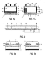
- Fig. 1 shows a diagrammatic cross-section of a part of a display device 1 which shows the principle on which a display device according to the invention is based.
- a first fluid 5 and a second fluid 6 are provided, which are immiscible with each other.
- the first fluid 5 is for instance an alkane like hexadecane or as in this example a (silicone) oil.
- the second fluid 6 is electroconductive or polar, for instance water or a salt solution (e.g. a solution of KCl in a mixture of water and ethyl alcohol).
- a transparent electrode 7 for example indium (tin) oxide is provided and an intermediate less wettable (hydrophobic) layer 8, in this example an amorphous fluoropolymer (AF1600).
- Figure 2 shows an embodiment of a display device according to the invention, in which walls between separate picture elements have been omitted for the greater part for the sake of clarity.
- the pixel walls 13 do not extend across the whole pixel thickness.
- Such walls may be obtained by offset printing or other printing techniques known in the art.
- the oil film 5 is very stable, which is enhanced even further as the pixel size decreases. So during switching the oil remains confined in each area.
- the other reference numerals have the same meaning as those in Figure 1 .
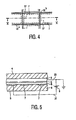
- the layer 13 in this example is approximately 20 ⁇ m thick or less and consists of a lower part 13 b , more wettable to the first fluid (hydrophobic) and an upper less wettable (hydrophilic) part 13 a (see Figure 3 ).
- the wetting of the lower part of the pixel wall by the oil ensures a homogeneous optical off -state.
- the pixel is activated the reversibility of oil movement due to the less wettable (hydrophilic) upper part is also maintained.
- the less wettable (hydrophilic) part or a surface part
- the layer thickness of approximately 20 ⁇ m or less is a significant improvement with respect to the 80 ⁇ m layer, leading to an improved brightness and speed. Furthermore, due to the absence of glue, the oil covers the entire pixel area, improving the optical contrast.
- the layer 13 or layer parts 13 a , 13 b in this example are printed.
- a printing process is very simple and flexible, thereby facilitating the fabrication of electrowetting displays at high resolutions significantly. In such a printing process it may be advantageous to use a pre-treatment of the substrate, such as a reactive ion-etching step using O 2 to make it more hydrophilic.
- the separating area between pixel areas has been integrated into the substrate by making interpixel areas 13'of the substrate less wettable to the first fluid (hydrophilic) for instance by means of laser radiation, a UV-ozone treatment or an oxygen-plasma treatment.
- the further reference numerals in Figures 4, 5 have the same meaning as those in the other examples.
- the possibility of oil in adjacent pixels mixing when both pixels are switched to the transparent state is avoided by incorporating a controlled oil motion by electromagnetic control, in this case by leaving apertures 17 in the electrodes 7.
- the display may be made reflective by adding a reflector as shown by dashed lines 14 in Figure 3 .
- the electrode configuration chosen here is merely an example.
- Other electrode configurations can be chosen, such as a circular geometry. Such a circular geometry is used in e.g. shutter applications and diaphragms.
Description
- The invention relates to an optical switch comprising at least one first fluid and a second fluid immiscible with each other within a space between a first transparent substrate and a second substrate, the second fluid being electroconductive or polar.
- In particular the invention relates to a display device comprising picture elements (pixels) having at least one first fluid and a second fluid immiscible with each other within a space between a first transparent substrate and a second substrate, the second fluid being electroconductive or polar.
- Optical switches may be used in shutter applications, diaphragms, but also in switchable color filters in e.g. display applications.
- Display devices like TFT-LCDs are used in laptop computers and in organizers, but also find an increasingly wider application in GSM telephones. Instead of LCDs, for example, (polymer) LED display devices are also being used.
- Apart from these display effects that are well established by now other display techniques are evolving like electrophoretic displays, which are suitable for paper white applications.
- Known prior art is represented by
US 4 079 368 . - The invention is based on a principle called electro-wetting. The invention provides new ways of using this principle in which one of the fluids in a first state adjoins a greater part of the first substrate and in the second state the other fluid at least partly adjoins the first substrate.
- If for instance a (first) fluid is a (colored) oil and the second (the other) fluid is water (due to interfacial tensions) a two layer system is provided which comprises a water layer and an oil layer. However, if a voltage is applied between the water and an electrode on the first support plate the oil layer moves aside or breaks up due to electrostatic forces. Since parts of the water now penetrate the oil layer the picture element becomes partly transparent.
- Display devices based on this principle have been described in PCT Application
WO 03/071346 NL 02.0129 - In practice however these pixel walls have a certain wall height of about 80 µm or more which has severe implications for the optical performance of small pixels in particular. The presence of such pixel walls results in an effectively reduced pixel area, since the area close to the walls does not contribute to the pixel brightness at the higher incoming angles. As a result, the total pixel will become less bright. This reduction of brightness will be more severe for smaller pixels. At a wall height of about 80 µm, the loss of brightness is about 10 -15 % for a 500 µm x 500 µm pixel.
- Moreover the walls are generally glued to the underlying surface. This underlying surface is often a fluoropolymer surface so the bonding is rather weak mechanically due to the fact that the fluoropolymer is very hydrophobic. Also the glue in between the walls and the fluoropolymer surface tends to move into the pixel area. In this case, the oil will not cover this part of the pixel, since the oil is repelled from the glue surface. These areas cause a considerable increase in reflectivity in the "black" off-state, thereby reducing the optical contrast.
- It is one of the objects of the present invention to overcome at least partly the above mentioned problems.
- To this end an optical device according to the invention comprises at one substrate within said space a surface area less wettable for the second fluid, the less wettable surface area being surrounded by areas having a more wettable surface area.
- Although not strictly necessary the less wettable surface area is preferably separated by more wettable surfaces provided on walls.
- By lowering the walls to 20 µm thickness, or less, the device can be operating in a range where the oil height upon contraction is in fact larger than the actual wall height. The inventors have experimentally confirmed that the oil remains within the pixel, due to the pinning of the oil/water interface at the bottom of the wall. In display applications the possibility of oil in adjacent pixels mixing when both pixels are switched can be avoided by incorporating a controlled oil motion e.g. by electromagnetic forces.
- These and other aspects of the invention are apparent from and will be elucidated with reference to the embodiments described hereinafter.
- In the drawings:
-
Figure 1 is a diagrammatic cross-section of a part of a display device, to show the principle on which a display device according to the invention is based, -
Figure 2 is another diagrammatic cross-section of a part of a display device according to the invention, -
Figure 3 is a diagrammatic cross-section of a part of a display device according to the invention, while -
Figure 4 is a plan views of a part of a further display device according to the invention and -
Figure 5 is a diagrammatic cross-section along line V -V inFigure 4 - The Figures are diagrammatic and not drawn to scale. Corresponding elements are generally denoted by the same reference numerals.
-
Fig. 1 shows a diagrammatic cross-section of a part of a display device 1 which shows the principle on which a display device according to the invention is based. Between twotransparent substrates first fluid 5 and asecond fluid 6 are provided, which are immiscible with each other. Thefirst fluid 5 is for instance an alkane like hexadecane or as in this example a (silicone) oil. Thesecond fluid 6 is electroconductive or polar, for instance water or a salt solution (e.g. a solution of KCl in a mixture of water and ethyl alcohol). - In a first state, when no external voltage is applied (Fig. la) the
fluids transparent substrate support plate transparent electrode 7, for example indium (tin) oxide is provided and an intermediate less wettable (hydrophobic)layer 8, in this example an amorphous fluoropolymer (AF1600). - When a voltage is applied (voltage source 9) via
interconnections layer 5 moves aside or breaks up into small droplets (Fig. 1b ). This occurs when the electrostatic energy gain is larger than the surface energy loss due to the creation of curved surfaces. As a very important aspect it was found that reversible switching between acontinuous film 5 covering thesupport plate 3 and a film adjoining thewall 2 is achieved by means of the electrical switching means (voltage source 9). -
Figure 2 shows an embodiment of a display device according to the invention, in which walls between separate picture elements have been omitted for the greater part for the sake of clarity. In this embodiment thepixel walls 13 do not extend across the whole pixel thickness. Such walls may be obtained by offset printing or other printing techniques known in the art. It appears that theoil film 5 is very stable, which is enhanced even further as the pixel size decreases. So during switching the oil remains confined in each area. The other reference numerals have the same meaning as those inFigure 1 . - The
layer 13 in this example is approximately 20 µm thick or less and consists of alower part 13b, more wettable to the first fluid (hydrophobic) and an upper less wettable (hydrophilic) part 13a (seeFigure 3 ). In this way the wetting of the lower part of the pixel wall by the oil ensures a homogeneous optical off -state. Then when the pixel is activated the reversibility of oil movement due to the less wettable (hydrophilic) upper part is also maintained. Especially the less wettable (hydrophilic) part (or a surface part) has been found to be essential for good switching. - The layer thickness of approximately 20 µm or less is a significant improvement with respect to the 80 µm layer, leading to an improved brightness and speed. Furthermore, due to the absence of glue, the oil covers the entire pixel area, improving the optical contrast. The
layer 13 orlayer parts - In the display of
Figures 4, 5 the separating area between pixel areas has been integrated into the substrate by making interpixel areas 13'of the substrate less wettable to the first fluid (hydrophilic) for instance by means of laser radiation, a UV-ozone treatment or an oxygen-plasma treatment. The further reference numerals inFigures 4, 5 have the same meaning as those in the other examples. The possibility of oil in adjacent pixels mixing when both pixels are switched to the transparent state is avoided by incorporating a controlled oil motion by electromagnetic control, in this case by leavingapertures 17 in theelectrodes 7. - Several variations to the principle are possible. Although a transmissive device has been described, the display may be made reflective by adding a reflector as shown by dashed
lines 14 inFigure 3 . The electrode configuration chosen here is merely an example. Other electrode configurations can be chosen, such as a circular geometry. Such a circular geometry is used in e.g. shutter applications and diaphragms. - The invention resides in each and every novel characteristic feature and each and every combination of characteristic features. Reference numerals in the claims do not limit their protective scope. Use of the verb "to comprise" and its conjugations does not exclude the presence of elements other than those stated in the claims. Use of the article "a" or "an" preceding an element does not exclude the presence of a plurality of such elements.
Claims (5)
- A display device comprising- a first support plate (3) and a second support plate (4), at least one of which is transparent;- electrodes (7) provided on a first surface of the first support plate, the electrodes being spaced apart from each other;- an intermediate layer (8) provided on the electrodes (7) and on the first support plate in an area between said electrodes;- a space between the first support plate and the second support plate, the intermediate layer (8) facing the second support plate (4), and said space comprising a first fluid (5) and a second fluid (6) immiscible with each other, the second fluid (6) being electroconductive or polar;- pixel walls (13) provided on the intermediate layer (8) in the area between said electrodes, the pixel walls extending into said space but not extending to the second support plate;wherein the intermediate layer (8) is less wettable to the second fluid (6) than to the first fluid, surfaces provided on the pixel walls (13) are more wettable to the second fluid than to the first fluid and lower parts of the pixel walls adjacent to the intermediate layer are more wettable to the first fluid than to the second fluid.
- A display device according to Claim 1 in which the pixel walls have a height of at most 20 µm.
- A method for manufacturing an optical device according to claims 1 or 2, characterised by the step of making at least part of the first support plate more wettable to the second fluid by means of a pre-treatment.
- A method for manufacturing an optical device according to claim 3 including the step of providing the first support plate with pixel walls by means of a mold.
- A method for manufacturing an optical device according to claims 1, characterised by the step of making the pixel walls by means of a printing method.
Priority Applications (1)
| Application Number | Priority Date | Filing Date | Title |
|---|---|---|---|
| EP04732693.9A EP1629314B1 (en) | 2003-05-22 | 2004-05-13 | Display device |
Applications Claiming Priority (3)
| Application Number | Priority Date | Filing Date | Title |
|---|---|---|---|
| EP03101479 | 2003-05-22 | ||
| PCT/IB2004/050693 WO2004104670A1 (en) | 2003-05-22 | 2004-05-13 | Display device |
| EP04732693.9A EP1629314B1 (en) | 2003-05-22 | 2004-05-13 | Display device |
Publications (2)
| Publication Number | Publication Date |
|---|---|
| EP1629314A1 EP1629314A1 (en) | 2006-03-01 |
| EP1629314B1 true EP1629314B1 (en) | 2015-10-21 |
Family
ID=33462207
Family Applications (1)
| Application Number | Title | Priority Date | Filing Date |
|---|---|---|---|
| EP04732693.9A Active EP1629314B1 (en) | 2003-05-22 | 2004-05-13 | Display device |
Country Status (8)
| Country | Link |
|---|---|
| US (1) | US7529012B2 (en) |
| EP (1) | EP1629314B1 (en) |
| JP (1) | JP4610561B2 (en) |
| KR (1) | KR101100980B1 (en) |
| CN (1) | CN100405120C (en) |
| HK (1) | HK1090984A1 (en) |
| TW (1) | TWM275501U (en) |
| WO (1) | WO2004104670A1 (en) |
Families Citing this family (57)
| Publication number | Priority date | Publication date | Assignee | Title |
|---|---|---|---|---|
| US8319759B2 (en) | 2003-10-08 | 2012-11-27 | E Ink Corporation | Electrowetting displays |
| CN101930118B (en) * | 2003-10-08 | 2013-05-29 | 伊英克公司 | Electro-wetting displays |
| KR100531796B1 (en) * | 2003-12-10 | 2005-12-02 | 엘지전자 주식회사 | Optical shutter for plasma display panel and driving method therof |
| KR101293444B1 (en) * | 2004-04-05 | 2013-08-05 | 리쿠아비스타 비.브이. | Display device based on electrowetting effect |
| US8482496B2 (en) | 2006-01-06 | 2013-07-09 | Pixtronix, Inc. | Circuits for controlling MEMS display apparatus on a transparent substrate |
| US8159428B2 (en) | 2005-02-23 | 2012-04-17 | Pixtronix, Inc. | Display methods and apparatus |
| US9229222B2 (en) | 2005-02-23 | 2016-01-05 | Pixtronix, Inc. | Alignment methods in fluid-filled MEMS displays |
| US9082353B2 (en) * | 2010-01-05 | 2015-07-14 | Pixtronix, Inc. | Circuits for controlling display apparatus |
| US7502159B2 (en) * | 2005-02-23 | 2009-03-10 | Pixtronix, Inc. | Methods and apparatus for actuating displays |
| US8310442B2 (en) | 2005-02-23 | 2012-11-13 | Pixtronix, Inc. | Circuits for controlling display apparatus |
| US20070205969A1 (en) | 2005-02-23 | 2007-09-06 | Pixtronix, Incorporated | Direct-view MEMS display devices and methods for generating images thereon |
| US9261694B2 (en) | 2005-02-23 | 2016-02-16 | Pixtronix, Inc. | Display apparatus and methods for manufacture thereof |
| US8519945B2 (en) | 2006-01-06 | 2013-08-27 | Pixtronix, Inc. | Circuits for controlling display apparatus |
| US7999994B2 (en) | 2005-02-23 | 2011-08-16 | Pixtronix, Inc. | Display apparatus and methods for manufacture thereof |
| US9158106B2 (en) | 2005-02-23 | 2015-10-13 | Pixtronix, Inc. | Display methods and apparatus |
| JP5042865B2 (en) * | 2005-02-28 | 2012-10-03 | サムスン エルシーディ ネザーランド アールアンドディ センター ビー ヴィ | Display device |
| US7911681B2 (en) * | 2005-07-29 | 2011-03-22 | Dai Nippon Printing Co., Ltd. | Display device, its manufacturing method, and display medium |
| US8526096B2 (en) | 2006-02-23 | 2013-09-03 | Pixtronix, Inc. | Mechanical light modulators with stressed beams |
| GB0611134D0 (en) | 2006-06-06 | 2006-07-19 | Liquavista Bv | Optical apparatus |
| US9176318B2 (en) | 2007-05-18 | 2015-11-03 | Pixtronix, Inc. | Methods for manufacturing fluid-filled MEMS displays |
| JP5130726B2 (en) * | 2007-01-26 | 2013-01-30 | 大日本印刷株式会社 | Display device and display medium using the same |
| TWI363920B (en) * | 2007-05-25 | 2012-05-11 | Ind Tech Res Inst | Electrical field controlled surface tension displace devices and fabrication methods thereof |
| CN101393320B (en) * | 2007-09-21 | 2010-08-25 | 群康科技(深圳)有限公司 | Electric moisten display device |
| GB0720484D0 (en) * | 2007-10-19 | 2007-11-28 | Seereal Technologies Sa | Cells |
| CN101424783B (en) * | 2007-11-02 | 2010-09-29 | 群康科技(深圳)有限公司 | Electrowetting display |
| GB0723861D0 (en) | 2007-12-06 | 2008-01-23 | Liquavista Bv | Transflective electrowetting display device |
| JP2009211047A (en) * | 2008-02-05 | 2009-09-17 | Sony Corp | Liquid optical element |
| GB0807667D0 (en) | 2008-04-28 | 2008-06-04 | Liquavista Bv | Display device |
| US8520285B2 (en) | 2008-08-04 | 2013-08-27 | Pixtronix, Inc. | Methods for manufacturing cold seal fluid-filled display apparatus |
| TW201007321A (en) * | 2008-08-08 | 2010-02-16 | Wintek Corp | Electro-wetting display device |
| CN101666908B (en) * | 2008-09-04 | 2011-09-07 | 元太科技工业股份有限公司 | Pixel structure for displaying device and displaying device |
| US8169679B2 (en) | 2008-10-27 | 2012-05-01 | Pixtronix, Inc. | MEMS anchors |
| CN101750732B (en) * | 2008-12-08 | 2012-07-11 | 财团法人工业技术研究院 | Colored electroweting type display device |
| GB0822756D0 (en) | 2008-12-13 | 2009-01-21 | Eastman Kodak Co | Backlit display |
| TWI407146B (en) | 2009-06-10 | 2013-09-01 | Ind Tech Res Inst | Electrowetting display and method for fabricating the same |
| TWI422858B (en) * | 2009-09-04 | 2014-01-11 | Wintek Corp | Electrowetting pixel structure |
| TWI424192B (en) * | 2009-12-15 | 2014-01-21 | Au Optronics Corp | Electro-wetting display panel |
| DE102009059094A1 (en) | 2009-12-18 | 2011-06-22 | Seereal Technologies S.A. | Controllable spatial light modulator for use in spatial light modulation device of holographic display that is utilized in photo indicator, has field arranged outside optical path, where electrowetting on dielectrics cells are controllable |
| GB0922690D0 (en) * | 2009-12-30 | 2010-02-17 | Liquavista Bv | Electrowetting display device |
| TWI418849B (en) * | 2009-12-31 | 2013-12-11 | Wintek Corp | Electrowetting display and pixel array substrate thereof and electrowetting display pixel structure thereof |
| TW201122545A (en) * | 2009-12-31 | 2011-07-01 | Wintek Corp | Electrowetting display and pixel array substrate thereof and electrowetting display pixel structure thereof |
| BR112012019383A2 (en) | 2010-02-02 | 2017-09-12 | Pixtronix Inc | CIRCUITS TO CONTROL DISPLAY APPARATUS |
| US8723759B2 (en) | 2010-06-23 | 2014-05-13 | Sharp Kabushiki Kaisha | Display with light concentrating substrate |
| US8587858B2 (en) | 2011-05-23 | 2013-11-19 | Nokia Corporation | Apparatus and associated methods |
| EP2555039B1 (en) * | 2011-08-05 | 2017-08-23 | Samsung Electronics Co., Ltd. | Electrofluidic chromatophore (EFC) display apparatus |
| US8547623B2 (en) | 2011-11-22 | 2013-10-01 | Sharp Kabushiki Kaisha | Dual-mode electrowetting display device |
| GB201121710D0 (en) | 2011-12-16 | 2012-02-01 | Samsung Lcd Nl R & D Ct Bv | Electrowetting device |
| GB201121707D0 (en) | 2011-12-16 | 2012-02-01 | Samsung Lcd Nl R & D Ct Bv | Electrowetting display device |
| TWI442088B (en) * | 2012-02-24 | 2014-06-21 | Ind Tech Res Inst | Electrowetting display device |
| KR101952445B1 (en) * | 2012-05-10 | 2019-04-26 | 리쿠아비스타 비.브이. | Eloctro wetting display apparatus |
| KR101941165B1 (en) | 2012-06-07 | 2019-04-12 | 삼성전자주식회사 | Micro optical switch device, Image display apparatus comprising micro optical switch device and Methed of manufacturing micro optical switch device |
| US9134552B2 (en) | 2013-03-13 | 2015-09-15 | Pixtronix, Inc. | Display apparatus with narrow gap electrostatic actuators |
| JP6233596B2 (en) | 2013-09-09 | 2017-11-22 | パナソニックIpマネジメント株式会社 | Reflective display element |
| WO2015161433A1 (en) * | 2014-04-22 | 2015-10-29 | 深圳市国华光电科技有限公司 | Display structure having paper effect and manufacturing method therefor |
| CN104238106B (en) * | 2014-07-01 | 2017-04-26 | 陈明晖 | twisting ball display panel |
| CN107195781B (en) * | 2017-05-24 | 2020-07-07 | 华南师范大学 | PMMA-doped small molecule-based high-mobility transistor and preparation method thereof |
| CN110632752A (en) | 2019-09-27 | 2019-12-31 | Oppo广东移动通信有限公司 | Light gathering plate, light gathering display screen and mobile terminal |
Citations (2)
| Publication number | Priority date | Publication date | Assignee | Title |
|---|---|---|---|---|
| JP2000356750A (en) * | 1999-06-16 | 2000-12-26 | Canon Inc | Display element and display device |
| WO2003071346A1 (en) * | 2002-02-19 | 2003-08-28 | Koninklijke Philips Electronics N.V. | Display device |
Family Cites Families (12)
| Publication number | Priority date | Publication date | Assignee | Title |
|---|---|---|---|---|
| US4079368A (en) * | 1976-05-17 | 1978-03-14 | International Business Machines Corporation | Information display through deformation of liquid dielectric media |
| FR2524658A1 (en) * | 1982-03-30 | 1983-10-07 | Socapex | OPTICAL SWITCH AND SWITCHING MATRIX COMPRISING SUCH SWITCHES |
| JP2542750B2 (en) | 1985-12-09 | 1996-10-09 | 益弘 小駒 | Surface energy control method for plastics |
| JPH02196834A (en) * | 1989-01-25 | 1990-08-03 | Rikagaku Kenkyusho | Method for modifying surface of fluororesin with laser |
| US5956005A (en) * | 1995-12-29 | 1999-09-21 | Xerox Corporation | Electrocapillary display sheet which utilizes an applied electric field to move a liquid inside the display sheet |
| US5757345A (en) * | 1996-05-06 | 1998-05-26 | Xerox Corportion | Electrocapillary color display sheet |
| FR2769375B1 (en) * | 1997-10-08 | 2001-01-19 | Univ Joseph Fourier | VARIABLE FOCAL LENS |
| JP4532624B2 (en) * | 1999-06-16 | 2010-08-25 | キヤノン株式会社 | Optical element and photographing apparatus |
| US6449081B1 (en) * | 1999-06-16 | 2002-09-10 | Canon Kabushiki Kaisha | Optical element and optical device having it |
| JP3918371B2 (en) * | 1999-07-19 | 2007-05-23 | 富士ゼロックス株式会社 | Color filter, display element, display method, and display device |
| JP4424708B2 (en) * | 2000-02-17 | 2010-03-03 | キヤノン株式会社 | Optical system and photographing apparatus incorporating optical element, aperture or shutter in lens element |
| WO2003034748A1 (en) | 2001-10-11 | 2003-04-24 | Koninklijke Philips Electronics N.V. | 2d/3d display apparatus |
-
2004
- 2004-05-13 WO PCT/IB2004/050693 patent/WO2004104670A1/en active Application Filing
- 2004-05-13 US US10/557,378 patent/US7529012B2/en active Active
- 2004-05-13 JP JP2006530851A patent/JP4610561B2/en active Active
- 2004-05-13 CN CNB2004800138196A patent/CN100405120C/en active Active
- 2004-05-13 EP EP04732693.9A patent/EP1629314B1/en active Active
- 2004-05-13 KR KR1020057021912A patent/KR101100980B1/en active IP Right Grant
- 2004-05-19 TW TW093207870U patent/TWM275501U/en not_active IP Right Cessation
-
2006
- 2006-10-23 HK HK06111668.2A patent/HK1090984A1/en unknown
Patent Citations (3)
| Publication number | Priority date | Publication date | Assignee | Title |
|---|---|---|---|---|
| JP2000356750A (en) * | 1999-06-16 | 2000-12-26 | Canon Inc | Display element and display device |
| US6603444B1 (en) * | 1999-06-16 | 2003-08-05 | Canon Kabushiki Kaisha | Display element and display device having it |
| WO2003071346A1 (en) * | 2002-02-19 | 2003-08-28 | Koninklijke Philips Electronics N.V. | Display device |
Also Published As
| Publication number | Publication date |
|---|---|
| US20070127108A1 (en) | 2007-06-07 |
| TWM275501U (en) | 2005-09-11 |
| JP2007500876A (en) | 2007-01-18 |
| CN100405120C (en) | 2008-07-23 |
| JP4610561B2 (en) | 2011-01-12 |
| HK1090984A1 (en) | 2007-01-05 |
| WO2004104670A1 (en) | 2004-12-02 |
| KR20060014404A (en) | 2006-02-15 |
| EP1629314A1 (en) | 2006-03-01 |
| KR101100980B1 (en) | 2011-12-29 |
| US7529012B2 (en) | 2009-05-05 |
| CN1791823A (en) | 2006-06-21 |
Similar Documents
| Publication | Publication Date | Title |
|---|---|---|
| EP1629314B1 (en) | Display device | |
| EP1856571B1 (en) | Display device | |
| US9563052B2 (en) | Support plate of an electrowetting display | |
| EP1478974B1 (en) | Display device | |
| EP1629315B1 (en) | Display device | |
| EP1478972A1 (en) | Subtractive display device | |
| US8189267B2 (en) | Electrowetting display device | |
| US9019589B2 (en) | Electrowetting device | |
| WO2006021912A1 (en) | Display device based on immiscible fluids | |
| EP3049849A2 (en) | Electrowetting element | |
| WO2009100584A1 (en) | Liquid optical deflector and method for fabricating the same |
Legal Events
| Date | Code | Title | Description |
|---|---|---|---|
| PUAI | Public reference made under article 153(3) epc to a published international application that has entered the european phase |
Free format text: ORIGINAL CODE: 0009012 |
|
| 17P | Request for examination filed |
Effective date: 20051222 |
|
| AK | Designated contracting states |
Kind code of ref document: A1 Designated state(s): AT BE BG CH CY CZ DE DK EE ES FI FR GB GR HU IE IT LI LU MC NL PL PT RO SE SI SK TR |
|
| RAP1 | Party data changed (applicant data changed or rights of an application transferred) |
Owner name: LIQUAVISTA B.V. |
|
| DAX | Request for extension of the european patent (deleted) | ||
| 17Q | First examination report despatched |
Effective date: 20080930 |
|
| RAP1 | Party data changed (applicant data changed or rights of an application transferred) |
Owner name: LIQUAVISTA B.V. |
|
| 111L | Licence recorded |
Designated state(s): AT BE BG CH CY CZ DE DK EE ES FI FR GB GR HU IE IT LU MC NL PL PT RO SE SI SK TR Name of requester: MIORTECH HOLDING B.V., NL Effective date: 20110125 |
|
| RAP1 | Party data changed (applicant data changed or rights of an application transferred) |
Owner name: SAMSUNG LCD NETHERLANDS R&D CENTER B.V. |
|
| RAP1 | Party data changed (applicant data changed or rights of an application transferred) |
Owner name: LIQUAVISTA B.V. |
|
| REG | Reference to a national code |
Ref country code: DE Ref legal event code: R079 Ref document number: 602004048103 Country of ref document: DE Free format text: PREVIOUS MAIN CLASS: G02B0026020000 Ipc: G02B0026000000 |
|
| GRAP | Despatch of communication of intention to grant a patent |
Free format text: ORIGINAL CODE: EPIDOSNIGR1 |
|
| RIC1 | Information provided on ipc code assigned before grant |
Ipc: G02B 26/00 20060101AFI20150413BHEP Ipc: G02B 6/35 20060101ALI20150413BHEP |
|
| INTG | Intention to grant announced |
Effective date: 20150506 |
|
| GRAS | Grant fee paid |
Free format text: ORIGINAL CODE: EPIDOSNIGR3 |
|
| GRAA | (expected) grant |
Free format text: ORIGINAL CODE: 0009210 |
|
| 111L | Licence recorded |
Designated state(s): AT BE BG CH CY CZ DE DK EE ES FI FR GB GR HU IE IT LU MC NL PL PT RO SE SI SK TR Name of requester: MIORTECH HOLDING B.V., NL Effective date: 20110125 |
|
| AK | Designated contracting states |
Kind code of ref document: B1 Designated state(s): AT BE BG CH CY CZ DE DK EE ES FI FR GB GR HU IE IT LI LU MC NL PL PT RO SE SI SK TR |
|
| REG | Reference to a national code |
Ref country code: GB Ref legal event code: FG4D Ref country code: DE Ref legal event code: R081 Ref document number: 602004048103 Country of ref document: DE Owner name: AMAZON EUROPE HOLDING TECHNOLOGIES SCS, LU Free format text: FORMER OWNER: KONINKLIJKE PHILIPS ELECTRONICS N.V., EINDHOVEN, NL Ref country code: NL Ref legal event code: MP Effective date: 20151021 |
|
| REG | Reference to a national code |
Ref country code: CH Ref legal event code: PK Free format text: ERGAENZUNG LIZENZEINTRAG: NICHT AUSSCHLIESSLICHE LIZENZ Ref country code: CH Ref legal event code: EP |
|
| REG | Reference to a national code |
Ref country code: AT Ref legal event code: REF Ref document number: 756955 Country of ref document: AT Kind code of ref document: T Effective date: 20151115 |
|
| REG | Reference to a national code |
Ref country code: IE Ref legal event code: FG4D |
|
| REG | Reference to a national code |
Ref country code: DE Ref legal event code: R096 Ref document number: 602004048103 Country of ref document: DE |
|
| REG | Reference to a national code |
Ref country code: AT Ref legal event code: MK05 Ref document number: 756955 Country of ref document: AT Kind code of ref document: T Effective date: 20151021 |
|
| PG25 | Lapsed in a contracting state [announced via postgrant information from national office to epo] |
Ref country code: NL Free format text: LAPSE BECAUSE OF FAILURE TO SUBMIT A TRANSLATION OF THE DESCRIPTION OR TO PAY THE FEE WITHIN THE PRESCRIBED TIME-LIMIT Effective date: 20151021 Ref country code: ES Free format text: LAPSE BECAUSE OF FAILURE TO SUBMIT A TRANSLATION OF THE DESCRIPTION OR TO PAY THE FEE WITHIN THE PRESCRIBED TIME-LIMIT Effective date: 20151021 Ref country code: IT Free format text: LAPSE BECAUSE OF FAILURE TO SUBMIT A TRANSLATION OF THE DESCRIPTION OR TO PAY THE FEE WITHIN THE PRESCRIBED TIME-LIMIT Effective date: 20151021 |
|
| REG | Reference to a national code |
Ref country code: FR Ref legal event code: PLFP Year of fee payment: 13 |
|
| PG25 | Lapsed in a contracting state [announced via postgrant information from national office to epo] |
Ref country code: FI Free format text: LAPSE BECAUSE OF FAILURE TO SUBMIT A TRANSLATION OF THE DESCRIPTION OR TO PAY THE FEE WITHIN THE PRESCRIBED TIME-LIMIT Effective date: 20151021 Ref country code: SE Free format text: LAPSE BECAUSE OF FAILURE TO SUBMIT A TRANSLATION OF THE DESCRIPTION OR TO PAY THE FEE WITHIN THE PRESCRIBED TIME-LIMIT Effective date: 20151021 Ref country code: PT Free format text: LAPSE BECAUSE OF FAILURE TO SUBMIT A TRANSLATION OF THE DESCRIPTION OR TO PAY THE FEE WITHIN THE PRESCRIBED TIME-LIMIT Effective date: 20160222 Ref country code: PL Free format text: LAPSE BECAUSE OF FAILURE TO SUBMIT A TRANSLATION OF THE DESCRIPTION OR TO PAY THE FEE WITHIN THE PRESCRIBED TIME-LIMIT Effective date: 20151021 Ref country code: AT Free format text: LAPSE BECAUSE OF FAILURE TO SUBMIT A TRANSLATION OF THE DESCRIPTION OR TO PAY THE FEE WITHIN THE PRESCRIBED TIME-LIMIT Effective date: 20151021 Ref country code: GR Free format text: LAPSE BECAUSE OF FAILURE TO SUBMIT A TRANSLATION OF THE DESCRIPTION OR TO PAY THE FEE WITHIN THE PRESCRIBED TIME-LIMIT Effective date: 20160122 |
|
| REG | Reference to a national code |
Ref country code: DE Ref legal event code: R082 Ref document number: 602004048103 Country of ref document: DE Representative=s name: EIP EUROPE LLP, GB Ref country code: DE Ref legal event code: R081 Ref document number: 602004048103 Country of ref document: DE Owner name: AMAZON EUROPE HOLDING TECHNOLOGIES SCS, LU Free format text: FORMER OWNER: LIQUAVISTA B.V., EINDHOVEN, NL Ref country code: DE Ref legal event code: R082 Ref document number: 602004048103 Country of ref document: DE Representative=s name: EISENFUEHR SPEISER PATENTANWAELTE RECHTSANWAEL, DE |
|
| REG | Reference to a national code |
Ref country code: DE Ref legal event code: R082 Ref document number: 602004048103 Country of ref document: DE Representative=s name: EISENFUEHR SPEISER PATENTANWAELTE RECHTSANWAEL, DE |
|
| REG | Reference to a national code |
Ref country code: DE Ref legal event code: R097 Ref document number: 602004048103 Country of ref document: DE |
|
| RAP2 | Party data changed (patent owner data changed or rights of a patent transferred) |
Owner name: AMAZON EUROPE HOLDING TECHNOLOGIES SCS |
|
| PG25 | Lapsed in a contracting state [announced via postgrant information from national office to epo] |
Ref country code: CZ Free format text: LAPSE BECAUSE OF FAILURE TO SUBMIT A TRANSLATION OF THE DESCRIPTION OR TO PAY THE FEE WITHIN THE PRESCRIBED TIME-LIMIT Effective date: 20151021 |
|
| REG | Reference to a national code |
Ref country code: GB Ref legal event code: 732E Free format text: REGISTERED BETWEEN 20160707 AND 20160713 |
|
| PLBE | No opposition filed within time limit |
Free format text: ORIGINAL CODE: 0009261 |
|
| STAA | Information on the status of an ep patent application or granted ep patent |
Free format text: STATUS: NO OPPOSITION FILED WITHIN TIME LIMIT |
|
| PG25 | Lapsed in a contracting state [announced via postgrant information from national office to epo] |
Ref country code: EE Free format text: LAPSE BECAUSE OF FAILURE TO SUBMIT A TRANSLATION OF THE DESCRIPTION OR TO PAY THE FEE WITHIN THE PRESCRIBED TIME-LIMIT Effective date: 20151021 Ref country code: DK Free format text: LAPSE BECAUSE OF FAILURE TO SUBMIT A TRANSLATION OF THE DESCRIPTION OR TO PAY THE FEE WITHIN THE PRESCRIBED TIME-LIMIT Effective date: 20151021 Ref country code: BE Free format text: LAPSE BECAUSE OF NON-PAYMENT OF DUE FEES Effective date: 20160531 Ref country code: RO Free format text: LAPSE BECAUSE OF FAILURE TO SUBMIT A TRANSLATION OF THE DESCRIPTION OR TO PAY THE FEE WITHIN THE PRESCRIBED TIME-LIMIT Effective date: 20151021 Ref country code: SK Free format text: LAPSE BECAUSE OF FAILURE TO SUBMIT A TRANSLATION OF THE DESCRIPTION OR TO PAY THE FEE WITHIN THE PRESCRIBED TIME-LIMIT Effective date: 20151021 |
|
| 26N | No opposition filed |
Effective date: 20160722 |
|
| PG25 | Lapsed in a contracting state [announced via postgrant information from national office to epo] |
Ref country code: SI Free format text: LAPSE BECAUSE OF FAILURE TO SUBMIT A TRANSLATION OF THE DESCRIPTION OR TO PAY THE FEE WITHIN THE PRESCRIBED TIME-LIMIT Effective date: 20151021 |
|
| PG25 | Lapsed in a contracting state [announced via postgrant information from national office to epo] |
Ref country code: BE Free format text: LAPSE BECAUSE OF FAILURE TO SUBMIT A TRANSLATION OF THE DESCRIPTION OR TO PAY THE FEE WITHIN THE PRESCRIBED TIME-LIMIT Effective date: 20151021 Ref country code: LU Free format text: LAPSE BECAUSE OF FAILURE TO SUBMIT A TRANSLATION OF THE DESCRIPTION OR TO PAY THE FEE WITHIN THE PRESCRIBED TIME-LIMIT Effective date: 20160513 |
|
| REG | Reference to a national code |
Ref country code: CH Ref legal event code: PL |
|
| PG25 | Lapsed in a contracting state [announced via postgrant information from national office to epo] |
Ref country code: LI Free format text: LAPSE BECAUSE OF NON-PAYMENT OF DUE FEES Effective date: 20160531 Ref country code: CH Free format text: LAPSE BECAUSE OF NON-PAYMENT OF DUE FEES Effective date: 20160531 |
|
| REG | Reference to a national code |
Ref country code: IE Ref legal event code: MM4A |
|
| REG | Reference to a national code |
Ref country code: FR Ref legal event code: PLFP Year of fee payment: 14 |
|
| REG | Reference to a national code |
Ref country code: FR Ref legal event code: TP Owner name: AMAZON EUROPE HOLDING TECHNOLOGIES SCS, LU Effective date: 20170424 |
|
| PG25 | Lapsed in a contracting state [announced via postgrant information from national office to epo] |
Ref country code: IE Free format text: LAPSE BECAUSE OF NON-PAYMENT OF DUE FEES Effective date: 20160513 |
|
| REG | Reference to a national code |
Ref country code: FR Ref legal event code: PLFP Year of fee payment: 15 |
|
| PG25 | Lapsed in a contracting state [announced via postgrant information from national office to epo] |
Ref country code: HU Free format text: LAPSE BECAUSE OF FAILURE TO SUBMIT A TRANSLATION OF THE DESCRIPTION OR TO PAY THE FEE WITHIN THE PRESCRIBED TIME-LIMIT; INVALID AB INITIO Effective date: 20040513 Ref country code: CY Free format text: LAPSE BECAUSE OF FAILURE TO SUBMIT A TRANSLATION OF THE DESCRIPTION OR TO PAY THE FEE WITHIN THE PRESCRIBED TIME-LIMIT Effective date: 20151021 |
|
| PG25 | Lapsed in a contracting state [announced via postgrant information from national office to epo] |
Ref country code: MC Free format text: LAPSE BECAUSE OF FAILURE TO SUBMIT A TRANSLATION OF THE DESCRIPTION OR TO PAY THE FEE WITHIN THE PRESCRIBED TIME-LIMIT Effective date: 20151021 Ref country code: TR Free format text: LAPSE BECAUSE OF FAILURE TO SUBMIT A TRANSLATION OF THE DESCRIPTION OR TO PAY THE FEE WITHIN THE PRESCRIBED TIME-LIMIT Effective date: 20151021 |
|
| PG25 | Lapsed in a contracting state [announced via postgrant information from national office to epo] |
Ref country code: BG Free format text: LAPSE BECAUSE OF FAILURE TO SUBMIT A TRANSLATION OF THE DESCRIPTION OR TO PAY THE FEE WITHIN THE PRESCRIBED TIME-LIMIT Effective date: 20151021 |
|
| P01 | Opt-out of the competence of the unified patent court (upc) registered |
Effective date: 20230523 |
|
| PGFP | Annual fee paid to national office [announced via postgrant information from national office to epo] |
Ref country code: FR Payment date: 20230525 Year of fee payment: 20 Ref country code: DE Payment date: 20230530 Year of fee payment: 20 |
|
| PGFP | Annual fee paid to national office [announced via postgrant information from national office to epo] |
Ref country code: GB Payment date: 20230529 Year of fee payment: 20 |