EP1516224B1 - Enhancement electrode configuration for electrically controlled light modulators - Google Patents
Enhancement electrode configuration for electrically controlled light modulators Download PDFInfo
- Publication number
- EP1516224B1 EP1516224B1 EP02743283A EP02743283A EP1516224B1 EP 1516224 B1 EP1516224 B1 EP 1516224B1 EP 02743283 A EP02743283 A EP 02743283A EP 02743283 A EP02743283 A EP 02743283A EP 1516224 B1 EP1516224 B1 EP 1516224B1
- Authority
- EP
- European Patent Office
- Prior art keywords
- electrode structure
- enhancement
- signal
- cell
- layer
- Prior art date
- Legal status (The legal status is an assumption and is not a legal conclusion. Google has not performed a legal analysis and makes no representation as to the accuracy of the status listed.)
- Expired - Lifetime
Links
- 230000005684 electric field Effects 0.000 claims abstract description 37
- 229920000642 polymer Polymers 0.000 claims description 52
- 239000000463 material Substances 0.000 claims description 9
- 238000000034 method Methods 0.000 claims description 6
- 239000003190 viscoelastic substance Substances 0.000 claims description 6
- AMGQUBHHOARCQH-UHFFFAOYSA-N indium;oxotin Chemical compound [In].[Sn]=O AMGQUBHHOARCQH-UHFFFAOYSA-N 0.000 claims description 3
- 229920001296 polysiloxane Polymers 0.000 claims description 2
- 150000001875 compounds Chemical class 0.000 claims 1
- 239000012141 concentrate Substances 0.000 abstract 1
- 230000003287 optical effect Effects 0.000 description 15
- 238000004088 simulation Methods 0.000 description 11
- 239000000758 substrate Substances 0.000 description 10
- 238000009413 insulation Methods 0.000 description 9
- 239000003989 dielectric material Substances 0.000 description 6
- 230000000694 effects Effects 0.000 description 6
- 239000011521 glass Substances 0.000 description 6
- 239000002861 polymer material Substances 0.000 description 6
- 239000004020 conductor Substances 0.000 description 5
- 239000000126 substance Substances 0.000 description 5
- 238000006073 displacement reaction Methods 0.000 description 4
- 238000004519 manufacturing process Methods 0.000 description 4
- 238000005457 optimization Methods 0.000 description 3
- VYPSYNLAJGMNEJ-UHFFFAOYSA-N Silicium dioxide Chemical compound O=[Si]=O VYPSYNLAJGMNEJ-UHFFFAOYSA-N 0.000 description 2
- 239000012212 insulator Substances 0.000 description 2
- 230000002093 peripheral effect Effects 0.000 description 2
- PNEYBMLMFCGWSK-UHFFFAOYSA-N aluminium oxide Inorganic materials [O-2].[O-2].[O-2].[Al+3].[Al+3] PNEYBMLMFCGWSK-UHFFFAOYSA-N 0.000 description 1
- 230000000903 blocking effect Effects 0.000 description 1
- 230000015556 catabolic process Effects 0.000 description 1
- 229910052681 coesite Inorganic materials 0.000 description 1
- 238000005094 computer simulation Methods 0.000 description 1
- 238000010276 construction Methods 0.000 description 1
- 229910052593 corundum Inorganic materials 0.000 description 1
- 229910052906 cristobalite Inorganic materials 0.000 description 1
- 230000009849 deactivation Effects 0.000 description 1
- 238000006731 degradation reaction Methods 0.000 description 1
- 238000005516 engineering process Methods 0.000 description 1
- 230000000149 penetrating effect Effects 0.000 description 1
- 230000002040 relaxant effect Effects 0.000 description 1
- 239000000377 silicon dioxide Substances 0.000 description 1
- 229910052682 stishovite Inorganic materials 0.000 description 1
- 238000006467 substitution reaction Methods 0.000 description 1
- 239000012780 transparent material Substances 0.000 description 1
- 229910052905 tridymite Inorganic materials 0.000 description 1
- 239000011345 viscous material Substances 0.000 description 1
- 229910001845 yogo sapphire Inorganic materials 0.000 description 1
Images


Classifications
-
- G—PHYSICS
- G02—OPTICS
- G02B—OPTICAL ELEMENTS, SYSTEMS OR APPARATUS
- G02B26/00—Optical devices or arrangements for the control of light using movable or deformable optical elements
- G02B26/004—Optical devices or arrangements for the control of light using movable or deformable optical elements based on a displacement or a deformation of a fluid
-
- G—PHYSICS
- G02—OPTICS
- G02B—OPTICAL ELEMENTS, SYSTEMS OR APPARATUS
- G02B26/00—Optical devices or arrangements for the control of light using movable or deformable optical elements
- G02B26/02—Optical devices or arrangements for the control of light using movable or deformable optical elements for controlling the intensity of light
-
- G—PHYSICS
- G03—PHOTOGRAPHY; CINEMATOGRAPHY; ANALOGOUS TECHNIQUES USING WAVES OTHER THAN OPTICAL WAVES; ELECTROGRAPHY; HOLOGRAPHY
- G03H—HOLOGRAPHIC PROCESSES OR APPARATUS
- G03H2225/00—Active addressable light modulator
- G03H2225/20—Nature, e.g. e-beam addressed
- G03H2225/24—Having movable pixels, e.g. microelectromechanical systems [MEMS]
-
- G—PHYSICS
- G03—PHOTOGRAPHY; CINEMATOGRAPHY; ANALOGOUS TECHNIQUES USING WAVES OTHER THAN OPTICAL WAVES; ELECTROGRAPHY; HOLOGRAPHY
- G03H—HOLOGRAPHIC PROCESSES OR APPARATUS
- G03H2225/00—Active addressable light modulator
- G03H2225/30—Modulation
- G03H2225/32—Phase only
Definitions
- the present invention relates to electrically controlled light modulator devices according to the preamble of the appended claim 1.
- Document WO 01/48531 discloses a display panel structure (see especially Figs 49 to 55) in the form of an array of cells each of which comprises two deformable dielectric layers, which meet at a common interface.
- One of said dielectrics can be air ; the other is preferably polymer material acting as a relief forming gel.
- a support electrode structure is arranged on one side (below) of said dielectric layers and a second electrode structure, a signal electrode structure on the other side (above) of said layers, there being means for providing signals to the signal electrodes in order to create electric fields through the two dielectric layers and to further create surface reliefs on the gel surface at the interface of said two dielectrics.
- the periodical, sinusoidally varying reliefs created on the gel surface in each of the cells allows under the effect of light from a light source to create images on the display panel, which are viewable by the naked eye.
- FIG. 1 illustrates schematically the general principle of physics, which can be observed in connection with dielectric substances and which is also utilized in the aforementioned optical display device.
- Dielectric substance can be defined as a substance in which an electric field may be maintained with zero or near zero power dissipation, that is the electrical conductivity of the substance is zero or near zero.
- This ponderomotive force F is proportional to the square of the electric field E at that point. In the case of an interface between air and polymer, the ponderomotive force F acts onto the polymer surface into the direction of the air.
- the electric field generated between a support electrode and a signal electrode and penetrating through the interface of the two dielectrics within a light modulator cell is inhomogeneous over the polymer surface; the electric field is strongest directly under a signal electrode and weakest in the middle between two adjacent signal electrodes.
- This situation is valid for any practical dimensions of the light modulator cells and corresponding devices. Therefore, the force acting onto the polymer surface is inhomogeneous as well and a deformation of the polymer surface causing the surface to deviate from a flat plane can be observed.
- An optimum situation would be such that maximum ponderomotive force is reached directly under the center part of a signal electrode and correspondingly no force is applied in the middle between two adjacent signal electrodes.
- Figure 2 clarifies the aforementioned prior art solution by showing two adjacent pixels (cells) L,R in a possible pixel line of a display panel or corresponding light modulator device.
- Each pixel comprises several strip like signal electrodes 10 arranged parallel respect to each other on a substrate 11, which may be for example glass.
- Figure 2 shows an end view of the signal electrodes 10 thus revealing only the width and mutual distance between the electrodes 10.
- a dielectric and viscoelastic gel material 12 for example polymer, is applied onto a support electrode 14 and facing the signal electrodes 10.
- a gap 13 for example an air gap, is left between the surface of the viscoelastic layer 12 and the signal electrodes 10.
- the usually transparent support electrode 14 providing AC or DC potential is preferably made of indium tin oxide (ITO), as is known in the art, on the surface of a transparent front plate 15.
- the front plate 15 may be for example glass.
- the light may enter the structure depicted in Fig. 2 either through the front plate 15 or through the substrate 11.
- the device can be designed to operate either in transmissive or reflective mode depending on the light transmitting or reflecting properties of the various elements of the device.
- Fig. 2 the left pixel L is switched on by providing suitable voltage to the respective signal electrodes 10, whereas the right pixel R is switched off, that is no signal is fed to the signal electrodes 10 belonging to said pixel R.
- Arrows 16 marked for the left pixel L illustrate schematically the ponderomotive forces acting on the surface of the gel layer 12.
- the power consumption and thickness of the display devices should also be further reduced.
- the manufacturing technology of the display devices should be simple in order to allow lower prices.
- the displays should also be fast enough to be able to display video or similar fast changing image content without degration of the image quality.
- the aforementioned requirements also apply on other light modulator devices than display panels.
- Other applications which may be based on the use of electrically controlled deformation of dielectric and viscoelastic transparent materials include, but are not limited to, electrically controlled diffractive or refractive lenses, or electrically reconfigurable optical waveguide couplers.
- the main purpose of the present invention is to present a novel electrode configuration for light modulator cells based on the use of dielectric and viscoelastic materials to facilitate enhanced and active deformation of viscoelastic material in order to, among other things, increase the diffraction efficiency of the light modulator cells, shorten the response time required to switch a cell (pixel) or corresponding primary optical unit between on and off states, and to reduce the voltage levels required for a defined diffraction amplitude, that is for a certain height of a gel relief. Therefore, the current invention aims to the manufacturing of light modulators with better optical contrast, higher switching speed and smaller power consumption than what can be provided by devices of prior art. The invention also allows the use of softer polymers once more increasing the diffraction amplitude of the gel relief with the named advantages.
- the electrically controlled light modulator device is primarily characterized in what will be presented in the characterizing part of the independent claim 1.
- the basic idea of the invention is to utilize active fieldshaping enhancement electrode structure located in the proximity and in addition to the signal electrode structure of a cell in order to affect the electric field between the signal electrode structure and the support electrode structure and through the viscoelastic layer in a manner that the deformation amplitude of the viscoelastic layer in the cell is increased.
- the invention has the following two principal emdodiments: An in-plane-type enhancement electrode configuration and a sandwich-type enhancement electrode configuration.
- the signal electrode structures and the enhancement electrode structures are located side by side substantially in a single common plane facing the opposite support electrode structure.
- This embodiment of the invention describes a quite strict configuration but on the other hand it is easy to manufacture.
- the signal electrode structure and the enhancement electrode structure are located in different layers, that is in different planes respect to each other and respect to the opposite support electrode structure.
- a conductor plated glass substrate is used, where the whole conductor layer is utilized as an enhancement electrode.
- a thin dielectric insulation layer is further disposed and the signal electrodes are lithographically generated onto said dielectric insulation layer.
- the concept of a cell corresponds closely to a single pixel of a display.
- the invention is not limited to display devices, but can be applied broadly also to other type of light modulators. Therefore, the term cell is mainly used in the following description.
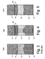
- Figures 3-5 illustrate schematically a single sub-cell cell structure used for the numerical computer simulations.
- the sub-cell comprises one signal electrode 10 plus half the spacing to the next adjacent signal electrode on each side. Therefore, a complete cell comprises in this example case all together three adjacent signal electrodes in a manner similar than presented in Fig. 2 .
- a practical cell (or pixel) can comprise also more than two sub-cells, for example, 5 or more sub-cells.
- the numerical simulations were decided to be performed using half-sub-cells instead complete sub-cells for the obvious reasons that this significantly increases simulation speed and reduces computer memory requirements without losing any relevant information due to the center symmetry of the sub-cell.
- Figs 3-5 are simplified and show only the basic parts of the light modulator structure: support electrodes 14, polymer gel layer 12, air gap 13, signal electrode 10 and substrate material 11.
- Figure 3 corresponds in general manner to the solution of prior art ( Fig. 2 ), disclosed for example in WO 01/48531 , and without the use of any active field enhancement electrodes. It can be seen that in this case when the signal electrode 10 is energized, the electric field illustrated with arrow-ended field lines spreads out from the area directly below the narrow signal electrode 10 due to the peripheral field (edge) effects, which take place in the area between the adjacent signal electrodes 10.
- Figure 4 shows the effect of a sandwich-type enhancement electrode 40 in a situation where the cell is switched on, that is the signal electrode 10 is energized.
- the enhancement electrode 40 arranged near to the signal electrode 10 changes the electric field between the signal electrode 10 and the support electrode 14. With the location and the potential of the enhancement electrode 40 chosen correctly, the electric field is altered in such a way that the electric field is concentrated directly below the signal electrode 10 and the peripheral effects outside the aforementioned area are reduced. This significantly increases the amplitude of the deformation of the gel layer 12 compared to the situation illustrated in Fig. 3 .
- the enhancement electrode plane above the signal electrode plane is separated by a thin dielectric insulator layer 41, which maybe, for example, an Al 2 O 3 or SiO 2 layer.
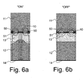
- Figures 6a and 6b show schematically an in-plane-type enhancement electrode configuration in on and off states, respectively.
- the in-plane-type configuration of the enhancement electrodes increases the efficiency of deformation nearly equally compared to the sandwich-type configuration shown in Figs. 4 and 5 .
- the enhancement electrodes 50 are arranged parallel on both sides of the signal electrode 10 in a common plane.
- an active enhancement electrode 50 is located in between every two adjacent signal electrodes 10.
- a thin dielectric insulator layer 51 since without such insulation said electrodes 10,50 would face directly the air of the air gap 13 and thus experience a low break-through voltage.
- the enhancement electrodes 40,50 do not need to be on ground potential. Simulations have showed that for the sandwich- and in-plane-type enhancement electrode configurations, a slightly negative potential is optimum for the enhancement electrodes 40,50 when the support electrode 14 is on ground potential and the signal electrodes 10 run at some tens to hundreds of volts.
- a defined minimum deformation (diffraction) amplitude for the polymer layer 12 is necessary. This minimum diffraction amplitude depends on several parameters of which one is the signal electrode 10 voltage. Since the invention creates significantly larger diffraction amplitudes at the same signal electrode voltage, the voltage may now be reduced to produce the same minimum diffraction amplitude needed for a working light modulator cell. Hence, because smaller voltage amplitudes can be created faster than large ones (limiting parameter V/ ⁇ s), increased switch-on speed of the light modulator can be observed together with smaller power consumption.
- the effect of the enhancement electrodes 40,50 can be understood best through the concept of electric field concentration. Due to the electric field concentration, only the polymer 12 in areas of strong electric field, that is directly below signal electrode 10 is drawn towards the air gap 13. At the same time the force onto the polymer 12 surface in the adjacent areas, that is areas not below the signal electrode 10, is reduced. Since the polymer material 12 is substantially incompressible, a polymer flow from the aforementioned areas of weak electric field to the areas of strong electric field takes place, and correspondingly significantly higher polymer layer 12 deformation amplitude can be seen. Without the enhancement electrodes 40,50, the electric field dynamics are much smaller; the polymer 12 remains under stress also at the sub-cell sides, hindering it from flowing freely to the area below the signal electrode 10.
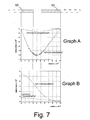
- Figure 7 shows horizontal (E x -field, Graph A) and vertical (Ey -field, Graph B) electric fields 250 nm above the polymer-air interface 12,13 of an in-plane enhancement electrode implementation shown schematically in Figs 6a,6b .
- the distance between the enhancement electrode 50 and the signal electrode 10 is 2 ⁇ m.
- Figure 7 corresponds therefore to half of a sub-cell presented in Figs 6a,6b .
- the horizontal E x -field shown in Graph A is a magnitude smaller than the vertical Ey-field shown in Graph B.
- Fig. 7 also includes electric fields corresponding a prior art situation, in other words without the enhancement electrodes.
- the enhancement electrodes 50 reduce significantly or remove almost completely the electric field beside the signal electrodes 10 and therefore allow the upward movement of the polymer 12 in the area directly below the signal electrodes 10. A higher deformation amplitude is resulted.
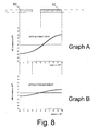
- Figure 8 shows the displacement of the polymer 12 surface in manner similar than Fig 7 .
- Graph A in Fig. 8 describes the situation with in-plane-type enhancement electrodes 50 activated and Graph B in Fig. 8 corresponds to the prior art situation without enhancement electrodes.
- the displacement in y-axis in both figures is given in micrometers.
- a slightly more negative potential for the enhancement electrodes 50 relative to the support electrode 14 improves performance. Other parameters are similar in both simulations.
- FIG. 8 the use of enhancement electrodes according to the invention clearly provides a much higher deformation amplitude.
- a very important feature of the invention is that it provides possibility to use active off switching instead of relying only on then natural relaxation of the polymer layer 12 after deactivation of the signal electrodes 10. This is a major difference compared to any prior art solutions, because it allows the use of softer polymer materials in the deformable layer 12 instead of typical harder polymers in order to produce larger diffraction amplitudes or, alternatively, lower signal voltages for similar, "standard” diffraction amplitudes.
- the "soft” polymer relaxes much slower than a "hard” polymer, and in order to prevent degradation of the response times of the system, active off switching is necessary.
- One parameter describing the aforementioned softness/hardness of a polymer is the elastic modulus of the material.
- the basic idea behind the active off switching according to the invention is the following: when the signal electrode 10 is switched off, the enhancement electrodes 40,50 are switched on for a short period of time until the polymer layer 12 just flattens out. This becomes possible because the electric field created by the enhancement electrodes especially in the in-plane-type configuration are located there, where the signal electrodes 10 create a polymer valley region. In other words, during on switching the polymer 12 beside the signal electrodes 10 was drawn to the area directly below the signal electrodes 10 in order to generate the diffraction peak. Naturally, this leaves a valley in the polymer layer 12 beside the signal electrodes 10, and for example in Fig. 6 directly under the in-plane-type enhancement electrodes 50.
- the enhancement electrodes 50 are provided for a short time with a suitable (high) voltage, this pulls actively the missing polymer back to fill up that valley, which results in an actively flattened polymer surface; the optical cell (pixel) is switched off much faster than through its natural slow relaxation due to the internal forces of the polymer.
- Fig. 5 Active off switching in the case of the sandwich-type enhancement electrode configuration is illustrated in Fig. 5 , where the pulling of the polymer layer 12 upwards beside the signal electrode 10 is somewhat exaggerated for demonstration purposes.
- the invention proposes a novel and inventive use of active enhancement electrodes, which provide at least the following significant benefits over prior art:
- Suitable dielectric and viscoelastic materials 12 include, for example, silicone gel, oil, various polymer materials or other viscous substances that have a tendency to deform when placed in a presence of an electric field, and said materials relax towards their original form or shape after the aforementioned effect ceases.
- the transparent electrode structures may be made of indium tin oxide (ITO), as is known in the art, or other methods for creating substantially transparent electrode structures on any substantially transparent substrate material can also be employed without departing from the scope of the present invention. If the device is designed to be used in reflection, or the electrode structures are designed to be small enough to cause only minor light blockage, it is also possble to use non-transparent electrode systems for the various electrodes.
- ITO indium tin oxide
- the support electrode structure, the signal electrode structure and also the enhancement electrode structure may be each composed of one or more separate electrode zones.
- Optimization parameters that may be selected according to the specific application, for a given signal electrode structure, include for example the number and width of the enhancement electrodes 40,50, the distance between the enhancement electrodes 40,50 and the signal electrodes 10.
- the enhancement electrode 40,50 voltage also is a parameter for optimization depending on voltage applied to the signal electrodes 10 and support electrodes 14.
- the sandwich-type implementation shown schematically in Figs 4 and 5 may use a conductor plated glass substrate 11, where the whole conductor layer is used as an enhancement electrode 40.
- a thin dielectric insulation layer 41 is disposed onto the enhancement electrode layer 40.
- the signal electrodes 10 are lithographically generated. No further insulation layers are needed to prevent electric break-through between said electrodes. Optimization parameters here include the thickness of the dielectric insulation layer 11, and as above, the voltage level of the enhancement electrode 40.
- the signal 10 and enhancement electrodes 50 may be lithographically generated on a conductor plated glass substrate 11.
- a dielectric insulation layer 51 is disposed onto the electrodes 10,50. Only small openings through the dielectric insulation layer 51 need to be arranged for contacting electrically said electrodes 10,50.
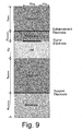
- Figure 9 corresponds to a sandwich-type configuration and Fig. 10 to an in-plane-type configuration.
- a typical number of sub-cells per pixel/cell depends on the application. For example, in case of a micro display one pixel (cell) could have dimensions 200 ⁇ m x 200 ⁇ m. This would lead to a construction with 5 - 50 sub-cells per pixel.
- the signal, support and enhancement electrode voltages depend on the mechanical dimensions of the cells as well as on the properties of the material of the viscoelastic layer. Table 2 gives certain voltage levels that can be regarded as target voltages for a micro display application. Table 1. Typical dimensions. Dimensions Abbreviation Typical Size Sandwich Typical Size In-Plane Airgap d air 3...5 ⁇ m 3... ⁇ m Polymer thickness d polymer 5...25 ⁇ m 5...25 ⁇ m opglass d glass 1mm 1 mm Substrate d substrate 2.3mm 2.3mm Signal electrode width W sig 2...20 ⁇ m 2...20 ⁇ m Enhancement electrode width W enh Pixel width 3...5 ⁇ m Electrode distance W sp X 2 ⁇ m Table 2. Typical voltages. Signal name Voltage OFF Voltage ON Signal 0 V 10...15 V Enhancement -60...-80 V -40...-20 V Support -80 V -80 V
- the electrically controlled light modulator and the various applications utilizing the same may be used for many types of optical switching purposes.
- the devices according to the invention can be used, for example, in display panels, electrically controlled lens elements or electrically reconfigurable optical couplers.
- the last mentioned devices might be used to switch or divide optical signal between several alternative targets, said targets being for example optical waveguides.
Abstract
Description
- The present invention relates to electrically controlled light modulator devices according to the preamble of the appended
claim 1. - Document
WO 01/48531 -
Figure 1 illustrates schematically the general principle of physics, which can be observed in connection with dielectric substances and which is also utilized in the aforementioned optical display device. Dielectric substance can be defined as a substance in which an electric field may be maintained with zero or near zero power dissipation, that is the electrical conductivity of the substance is zero or near zero. An electric field E going through an interface where dielectricity changes, such as the interface between air and polymer, causes a force F onto the surface of the dielectric having the higher dielectricity constant. This ponderomotive force F is proportional to the square of the electric field E at that point. In the case of an interface between air and polymer, the ponderomotive force F acts onto the polymer surface into the direction of the air. - The electric field generated between a support electrode and a signal electrode and penetrating through the interface of the two dielectrics within a light modulator cell is inhomogeneous over the polymer surface; the electric field is strongest directly under a signal electrode and weakest in the middle between two adjacent signal electrodes. This situation is valid for any practical dimensions of the light modulator cells and corresponding devices. Therefore, the force acting onto the polymer surface is inhomogeneous as well and a deformation of the polymer surface causing the surface to deviate from a flat plane can be observed. An optimum situation would be such that maximum ponderomotive force is reached directly under the center part of a signal electrode and correspondingly no force is applied in the middle between two adjacent signal electrodes. This would provide maximum height for the surface relief, because it allows the maximum flow of the polymer material towards the area where the electric field is strongest. The concept of polymer flow is essential here, since most polymers are substantially uncompressible and therefore cannot simply expand in volume under the effect of an electric field.
-
Figure 2 clarifies the aforementioned prior art solution by showing two adjacent pixels (cells) L,R in a possible pixel line of a display panel or corresponding light modulator device. Each pixel comprises several strip likesignal electrodes 10 arranged parallel respect to each other on asubstrate 11, which may be for example glass.Figure 2 shows an end view of thesignal electrodes 10 thus revealing only the width and mutual distance between theelectrodes 10. A dielectric andviscoelastic gel material 12, for example polymer, is applied onto asupport electrode 14 and facing thesignal electrodes 10. Agap 13, for example an air gap, is left between the surface of theviscoelastic layer 12 and thesignal electrodes 10. The usuallytransparent support electrode 14 providing AC or DC potential is preferably made of indium tin oxide (ITO), as is known in the art, on the surface of atransparent front plate 15. Thefront plate 15 may be for example glass. - The light may enter the structure depicted in
Fig. 2 either through thefront plate 15 or through thesubstrate 11. The device can be designed to operate either in transmissive or reflective mode depending on the light transmitting or reflecting properties of the various elements of the device. - In
Fig. 2 the left pixel L is switched on by providing suitable voltage to therespective signal electrodes 10, whereas the right pixel R is switched off, that is no signal is fed to thesignal electrodes 10 belonging to saidpixel R. Arrows 16 marked for the left pixel L illustrate schematically the ponderomotive forces acting on the surface of thegel layer 12. Through proper selection of thesignal electrode 10 dimensions (width) and mutual positioning (distance between adjacent and parallel electrodes) a sinusoidal surface structure, a surface relief can be created on thepolymer gel 12 surface. Illuminating light onto thesinusoidal gel 12 surface in pixel L through thefront plate 15 orsubstrate 11 refracts light into a slightly different direction than illuminating a plane gel surface in pixel R. By this means and using an optical blocking filter for the pixel in off state, a pixel can be electrically switched on and off. - The major shortcomings of the light modulators, like the display panels described in
WO 01/48531 - With the goal of bringing display quality closer to that of a paper print, for example brightness and contrast of the displays must be further improved. In order to allow the use of display devices in small-size portable devices, the power consumption and thickness of the display devices should also be further reduced. To make mass production of portable devices possible, the manufacturing technology of the display devices should be simple in order to allow lower prices. The displays should also be fast enough to be able to display video or similar fast changing image content without degration of the image quality. The aforementioned requirements also apply on other light modulator devices than display panels. Other applications which may be based on the use of electrically controlled deformation of dielectric and viscoelastic transparent materials include, but are not limited to, electrically controlled diffractive or refractive lenses, or electrically reconfigurable optical waveguide couplers.
- The main purpose of the present invention is to present a novel electrode configuration for light modulator cells based on the use of dielectric and viscoelastic materials to facilitate enhanced and active deformation of viscoelastic material in order to, among other things, increase the diffraction efficiency of the light modulator cells, shorten the response time required to switch a cell (pixel) or corresponding primary optical unit between on and off states, and to reduce the voltage levels required for a defined diffraction amplitude, that is for a certain height of a gel relief. Therefore, the current invention aims to the manufacturing of light modulators with better optical contrast, higher switching speed and smaller power consumption than what can be provided by devices of prior art. The invention also allows the use of softer polymers once more increasing the diffraction amplitude of the gel relief with the named advantages.
- To attain these purposes, the electrically controlled light modulator device according to the invention is primarily characterized in what will be presented in the characterizing part of the
independent claim 1. - The basic idea of the invention is to utilize active fieldshaping enhancement electrode structure located in the proximity and in addition to the signal electrode structure of a cell in order to affect the electric field between the signal electrode structure and the support electrode structure and through the viscoelastic layer in a manner that the deformation amplitude of the viscoelastic layer in the cell is increased.
- The invention has the following two principal emdodiments: An in-plane-type enhancement electrode configuration and a sandwich-type enhancement electrode configuration.
- In the in-plane-type configuration, the signal electrode structures and the enhancement electrode structures are located side by side substantially in a single common plane facing the opposite support electrode structure. This embodiment of the invention describes a quite strict configuration but on the other hand it is easy to manufacture.
- In the sandwich-type configuration, the signal electrode structure and the enhancement electrode structure are located in different layers, that is in different planes respect to each other and respect to the opposite support electrode structure. In a preferred embodiment of the sandwich-type electrode configuration, a conductor plated glass substrate is used, where the whole conductor layer is utilized as an enhancement electrode. Onto this enhancement electrode layer, a thin dielectric insulation layer is further disposed and the signal electrodes are lithographically generated onto said dielectric insulation layer.
- The preferred embodiments of the invention and their benefits will become more apparent to a person skilled in the art through the description and examples given herein below, and also through the appended claims.
- In the following, the invention will be described in more detail with reference to the appended drawings, in which
- Fig.1
- illustrates schematically force F acting on an interface between substances having different dielectricity under the influence of an electric field,
- Fig. 2
- illustrates schematically two adjacent pixels of a prior art display panel based on the use of electrically deformable dielectric viscoelastic gel,
- Fig. 3
- illustrates schematically a single sub-cell according to the prior art, including illustrations of electric field lines,
- Fig. 4
- illustrates schematically a single sub-cell according to the invention with sandwich-type enhancement electrode and the cell switched on, including illustrations of electric field lines
- Fig. 5
- same as
Fig. 4 but the cell switched off, - Fig. 6a
- illustrates schematically a single sub-cell according to the invention with in-plane-type enhancement electrode and switched on, including illustrations of electric field lines
- Fig 6b
- same as
Fig. 6a but the cell switched off, - Fig. 7
- presents simulation results comparing the horizontal (Graph A) and the vertical (Graph B) electric field strengths above the polymer surface in an in-plane-type enhancement electrode implementation and in a prior art type solution,
- Fig. 8
- presents a simulation result showing the polymer surface displacement in an in-plane-type, enhancement electrode implementation (Graph A), and a comparable simulation result showing the polymer surface displacement in a prior art solution (Graph B),
- Fig.9
- defines abbreviations for the various dimensions of a sandwich-type cell configuration,
- Fig. 10
- defines abbreviations for the various dimensions of a in-plane-type cell configuration.
- In the following, the enhancement electrode configurations according to the invention are described in more detail and their benefits compared to the prior art solutions are pointed out using selected simulation results.
- It should be noted that when the invention is applied to display devices, the concept of a cell corresponds closely to a single pixel of a display. However, the invention is not limited to display devices, but can be applied broadly also to other type of light modulators. Therefore, the term cell is mainly used in the following description.
-
Figures 3-5 illustrate schematically a single sub-cell cell structure used for the numerical computer simulations. The sub-cell comprises onesignal electrode 10 plus half the spacing to the next adjacent signal electrode on each side. Therefore, a complete cell comprises in this example case all together three adjacent signal electrodes in a manner similar than presented inFig. 2 . A practical cell (or pixel) can comprise also more than two sub-cells, for example, 5 or more sub-cells. The numerical simulations were decided to be performed using half-sub-cells instead complete sub-cells for the obvious reasons that this significantly increases simulation speed and reduces computer memory requirements without losing any relevant information due to the center symmetry of the sub-cell. - Compared to
Fig. 2 ,Figs 3-5 are simplified and show only the basic parts of the light modulator structure:support electrodes 14,polymer gel layer 12,air gap 13,signal electrode 10 andsubstrate material 11. -
Figure 3 corresponds in general manner to the solution of prior art (Fig. 2 ), disclosed for example inWO 01/48531 signal electrode 10 is energized, the electric field illustrated with arrow-ended field lines spreads out from the area directly below thenarrow signal electrode 10 due to the peripheral field (edge) effects, which take place in the area between theadjacent signal electrodes 10. -
Figure 4 shows the effect of a sandwich-type enhancement electrode 40 in a situation where the cell is switched on, that is thesignal electrode 10 is energized. Now according to the invention, theenhancement electrode 40 arranged near to thesignal electrode 10 changes the electric field between thesignal electrode 10 and thesupport electrode 14. With the location and the potential of theenhancement electrode 40 chosen correctly, the electric field is altered in such a way that the electric field is concentrated directly below thesignal electrode 10 and the peripheral effects outside the aforementioned area are reduced. This significantly increases the amplitude of the deformation of thegel layer 12 compared to the situation illustrated inFig. 3 . In order to allow thesignal electrode 10 and theenhancement electrode 40 to be arranged in different potentials, the enhancement electrode plane above the signal electrode plane is separated by a thindielectric insulator layer 41, which maybe, for example, an Al2O3 or SiO2 layer. -
Figures 6a and 6b show schematically an in-plane-type enhancement electrode configuration in on and off states, respectively. According to the simulations, the in-plane-type configuration of the enhancement electrodes increases the efficiency of deformation nearly equally compared to the sandwich-type configuration shown inFigs. 4 and 5 . InFigs 6a and 6b showing a sub-cell, theenhancement electrodes 50 are arranged parallel on both sides of thesignal electrode 10 in a common plane. In other words anactive enhancement electrode 50 is located in between every twoadjacent signal electrodes 10. To avoid electrical break-through between the signal- and enhancement electrodes they are covered with a thindielectric insulator layer 51, since without such insulation saidelectrodes air gap 13 and thus experience a low break-through voltage. - According to the invention, the
enhancement electrodes enhancement electrodes support electrode 14 is on ground potential and thesignal electrodes 10 run at some tens to hundreds of volts. - A very significant increase in the
polymer layer 12 deformation efficiency, that is higher deformation amplitudes can be expected through the use of theenhancement electrodes polymer layer 12 amplitude may be increased by a factor 6.5 without changing any other parameters expect the addition of theenhancement electrodes signal electrode 10 and thesupport electrodes 14. - To achieve a reasonable optical contrast between a light modulator cell being switched on and a light modulator cell being switched off, a defined minimum deformation (diffraction) amplitude for the
polymer layer 12 is necessary. This minimum diffraction amplitude depends on several parameters of which one is thesignal electrode 10 voltage. Since the invention creates significantly larger diffraction amplitudes at the same signal electrode voltage, the voltage may now be reduced to produce the same minimum diffraction amplitude needed for a working light modulator cell. Hence, because smaller voltage amplitudes can be created faster than large ones (limiting parameter V/µs), increased switch-on speed of the light modulator can be observed together with smaller power consumption. - The effect of the
enhancement electrodes polymer 12 in areas of strong electric field, that is directly belowsignal electrode 10 is drawn towards theair gap 13. At the same time the force onto thepolymer 12 surface in the adjacent areas, that is areas not below thesignal electrode 10, is reduced. Since thepolymer material 12 is substantially incompressible, a polymer flow from the aforementioned areas of weak electric field to the areas of strong electric field takes place, and correspondingly significantlyhigher polymer layer 12 deformation amplitude can be seen. Without theenhancement electrodes polymer 12 remains under stress also at the sub-cell sides, hindering it from flowing freely to the area below thesignal electrode 10. - In the following, some simulations results for in-plane-type enhancement electrodes are presented in order to compare their performance with the solutions of prior art.
-
Figure 7 shows horizontal (Ex -field, Graph A) and vertical (Ey -field, Graph B) electric fields 250 nm above the polymer-air interface Figs 6a,6b . InFig. 7 half of the 10 µmwide signal electrode 10 is located at the right side of the graphs from x=5 to x=10 and half of the 6 µmwide enhancement electrode 50 is in plane with thesignal electrode 10 and located on the left side of the graphs from location x=0 to x=3. The distance between theenhancement electrode 50 and thesignal electrode 10 is 2 µm.Figure 7 corresponds therefore to half of a sub-cell presented inFigs 6a,6b . The horizontal Ex-field shown in Graph A is a magnitude smaller than the vertical Ey-field shown in Graph B. For comparison,Fig. 7 also includes electric fields corresponding a prior art situation, in other words without the enhancement electrodes. - Especially from Graph B in
Fig. 7 showing the vertical Ey-field it is immediately clear that with theenhancement electrodes 50 the electric field is reduced at the sides of the sub-cell, that is outside the area directly below thesignal electrode 10. Below thesignal electrode 10, the field strength corresponds closely to the prior art situation without the enhancement electrodes. Keeping in mind that the forces acting onto thepolymer 12 surface are proportional to the square of the electric field strength, it is clear that the deeper gradient in the electric field between the area directly below the signal electrode 10 (x = 5-10) and outside that area (x = 0-5) make a major difference in thepolymer layer 12 behaviour. In the prior art situation without enhancement electrodes the polymer surface is under stress also beside (x = 0-5) thesignal electrodes 10, where it basically should be allowed to move freely downwards to compensate the polymer flow necessary for the upward movement below thesignal electrodes 10. Since thepolymer 12 cannot expand significantly in volume due to its incompressibility, the force onto thepolymer 12 surface beside thesignal electrodes 10 prohibits effectively said upward movement below thesignal electrode 10. Theenhancement electrodes 50 reduce significantly or remove almost completely the electric field beside thesignal electrodes 10 and therefore allow the upward movement of thepolymer 12 in the area directly below thesignal electrodes 10. A higher deformation amplitude is resulted. -
Figure 8 shows the displacement of thepolymer 12 surface in manner similar thanFig 7 . Graph A inFig. 8 describes the situation with in-plane-type enhancement electrodes 50 activated and Graph B inFig. 8 corresponds to the prior art situation without enhancement electrodes. The displacement in y-axis in both figures is given in micrometers. In order to get a fair comparison between the invention and the prior art solution, similar voltage differences between signal- and support electrodes have been used. Therefore, in Graph A Vsupport = - 150 V and Vsignal= 40 V and in Graph B Vsupport = - 150 V and Vsignal= 40 V. Theenhancement electrodes 50 in Graph A are provided with Venhancement = - 200 V. A slightly more negative potential for theenhancement electrodes 50 relative to thesupport electrode 14 improves performance. Other parameters are similar in both simulations. - It is evident from
Fig. 8 that the use of enhancement electrodes according to the invention clearly provides a much higher deformation amplitude. A very important feature of the invention is that it provides possibility to use active off switching instead of relying only on then natural relaxation of thepolymer layer 12 after deactivation of thesignal electrodes 10. This is a major difference compared to any prior art solutions, because it allows the use of softer polymer materials in thedeformable layer 12 instead of typical harder polymers in order to produce larger diffraction amplitudes or, alternatively, lower signal voltages for similar, "standard" diffraction amplitudes. Because the inner forces in a "soft" polymer are much smaller than in a "hard" polymer, the "soft" polymer relaxes much slower than a "hard" polymer, and in order to prevent degradation of the response times of the system, active off switching is necessary. One parameter describing the aforementioned softness/hardness of a polymer is the elastic modulus of the material. - The basic idea behind the active off switching according to the invention is the following: when the
signal electrode 10 is switched off, theenhancement electrodes polymer layer 12 just flattens out. This becomes possible because the electric field created by the enhancement electrodes especially in the in-plane-type configuration are located there, where thesignal electrodes 10 create a polymer valley region. In other words, during on switching thepolymer 12 beside thesignal electrodes 10 was drawn to the area directly below thesignal electrodes 10 in order to generate the diffraction peak. Naturally, this leaves a valley in thepolymer layer 12 beside thesignal electrodes 10, and for example inFig. 6 directly under the in-plane-type enhancement electrodes 50. Now, during off switching if theenhancement electrodes 50 are provided for a short time with a suitable (high) voltage, this pulls actively the missing polymer back to fill up that valley, which results in an actively flattened polymer surface; the optical cell (pixel) is switched off much faster than through its natural slow relaxation due to the internal forces of the polymer. - Active off switching in the case of the sandwich-type enhancement electrode configuration is illustrated in
Fig. 5 , where the pulling of thepolymer layer 12 upwards beside thesignal electrode 10 is somewhat exaggerated for demonstration purposes. - To shortly summarize the main aspects of the current invention, the invention proposes a novel and inventive use of active enhancement electrodes, which provide at least the following significant benefits over prior art:
- Higher efficiency: Smaller signal voltage levels are required to achieve required diffractive amplitude levels, that is amplitudes of viscoelastic layer deformations. Correspondingly, "standard" voltage levels may be used to achieve increased diffractive amplitudes.
- Increased response time: The
enhancement electrodes - While the invention has been shown and described above with respect to selected embodiments, it should be understood that these embodiments are only examples and that a person skilled in the art could construct other embodiments utilizing technical details other than those specifically disclosed herein while still remaining within the scope of the present invention as defined in the appended claims. It should therefore be understood that various omissions and substitutions and changes in the form and detail of the light modulator illustrated, as well as in the operation of the same, may be made by those skilled in the art without departing from the scope of the invention . It is the intention, therefore, to restrict the invention only in the manner indicated by the scope of the claims appended hereto.
- For example, the embodiments of the invention can be extended to devices where the
air gap 13 is replaced with a gap formed from some other suitable gas or vacuum or other deformable polymer. Suitable dielectric andviscoelastic materials 12 include, for example, silicone gel, oil, various polymer materials or other viscous substances that have a tendency to deform when placed in a presence of an electric field, and said materials relax towards their original form or shape after the aforementioned effect ceases. - The transparent electrode structures may be made of indium tin oxide (ITO), as is known in the art, or other methods for creating substantially transparent electrode structures on any substantially transparent substrate material can also be employed without departing from the scope of the present invention. If the device is designed to be used in reflection, or the electrode structures are designed to be small enough to cause only minor light blockage, it is also possble to use non-transparent electrode systems for the various electrodes.
- Within a single light modulator cell or corresponding primary optical unit the support electrode structure, the signal electrode structure and also the enhancement electrode structure may be each composed of one or more separate electrode zones.
- Optimization parameters that may be selected according to the specific application, for a given signal electrode structure, include for example the number and width of the
enhancement electrodes enhancement electrodes signal electrodes 10. Theenhancement electrode signal electrodes 10 andsupport electrodes 14. - The sandwich-type implementation shown schematically in
Figs 4 and 5 may use a conductor platedglass substrate 11, where the whole conductor layer is used as anenhancement electrode 40. Onto theenhancement electrode layer 40, a thindielectric insulation layer 41 is disposed. Onto thedielectric insulation layer 41, thesignal electrodes 10 are lithographically generated. No further insulation layers are needed to prevent electric break-through between said electrodes. Optimization parameters here include the thickness of thedielectric insulation layer 11, and as above, the voltage level of theenhancement electrode 40. - For the in-plane-type implementation shown schematically in
Figs 6a,6b , thesignal 10 andenhancement electrodes 50 may be lithographically generated on a conductor platedglass substrate 11. Adielectric insulation layer 51 is disposed onto theelectrodes dielectric insulation layer 51 need to be arranged for contacting electrically saidelectrodes - In table 1 selected examples of typical dimensions of the various structures in the enhancement electrode cells are given with reference to
Figs 9 and10 .Figure 9 corresponds to a sandwich-type configuration andFig. 10 to an in-plane-type configuration. - A typical number of sub-cells per pixel/cell depends on the application. For example, in case of a micro display one pixel (cell) could have dimensions 200µm x 200µm. This would lead to a construction with 5 - 50 sub-cells per pixel.
- The signal, support and enhancement electrode voltages depend on the mechanical dimensions of the cells as well as on the properties of the material of the viscoelastic layer. Table 2 gives certain voltage levels that can be regarded as target voltages for a micro display application.
Table 1. Typical dimensions. Dimensions Abbreviation Typical Size Sandwich Typical Size In- Plane Airgap d air 3... 5µm 3...µm Polymer thickness d polymer 5... 25µm 5...25µm opglass dglass 1mm 1 mm Substrate dsubstrate 2.3mm 2.3mm Signal electrode width W sig 2... 20µm 2...20µm Enhancement electrode width Wenh Pixel width 3...5µm Electrode distance Wsp X 2µm Table 2. Typical voltages. Signal name Voltage OFF Voltage ON Signal 0 V 10...15 V Enhancement -60...-80 V -40...-20 V Support -80 V -80 V - It is obvious for a person skilled in the art that the operation of the optical devices according to the invention on some applications rely on optical interference, and thus require a certain degree of coherence and/or collimation of the optical signal/beam that is being processed.
- The electrically controlled light modulator and the various applications utilizing the same may be used for many types of optical switching purposes. The devices according to the invention can be used, for example, in display panels, electrically controlled lens elements or electrically reconfigurable optical couplers. The last mentioned devices might be used to switch or divide optical signal between several alternative targets, said targets being for example optical waveguides.
Claims (12)
- A light modulating device comprising at least one cell, said cell comprising- two deformable dielectric layers (12,13) which meet at an interface, at least one of said layers being a viscoelastic layer (12) consisting of a viscoelastic relief forming material,- a first support electrode structure (14) arranged on one side of said dielectric layers (12,13).- a second signal electrode structure (10) arranged on the other side of said dielectric layers (12,13) and opposite said support electrode structure (14),- signal means for applying signal voltage between said support electrode structure (14) and said signal electrode structure (10) to generate an electric field passing through said two deformable dielectric layers (12,13) in order to create a surface relief on said viscoelastic layer (12),- a third enhancement electrode structure (40,50) arranged in the proximity of said first signal electrode structure (10), and- enhancement signal means for applying an enhancement signal voltage between said enhancement electrode structure (40, 50) and said signal electrode structure (10) in order to enhance the amplitude of deformation of said viscoelastic layer by locally concentrating the electric field passing through said two deformable dielectric layers (12,13),characterized in that said enhancement signal means is further arranged to apply a pulsed enhancement signal voltage between said enhancement electrode structure (40, 50) and said signal electrode structure (10) during flattening of said surface relief in order to enhance the relaxation of said viscoelastic layer (12).
- The light modulating device according to the claim 1, characterized in that within a cell said enhancement electrode structure (50) and said signal electrode structure (10) are arranged substantially in a single common plane.
- The light modulating device according to the claim 2, characterized in that within a cell a zone of said signal electrode structure is located between at least two zones of said enhancement electrode structure.
- The light modulating device according to the claim 1, characterized in that within a cell said enhancement electrode structure (40) and said signal electrode structure (10) are arranged in substantially different planes with respect to each other and with respect to said support electrode structure (14).
- The light modulating device according to any of the foregoing claims, characterized in that said enhancement electrode structure (40,50) is opaque.
- The light modulating device according to any of the foregoing claims 1 to 4, characterized in that said enhancement electrode structure (40,50) is an optically transparent structure formed of indium tin oxide.
- The light modulating device according to any of the foregoing claims, characterized in that an electrically insulating layer (41,51) is arranged on one or both sides of said enhancement electrode structure (40,50).
- The light modulating device according to any of the foregoing claims, characterized in that the material of the viscoelastic relief forming layer (12) is selected from the following group: polymer, silicone compound, oil.
- The light modulating device according to any of the foregoing claims, characterized in that a plurality of cells are arranged to form a display device.
- A method for modulating light by creating and flattening a relief in a viscoelastic material layer (12),
by using a cell, said cell comprising a support electrode structure a cell, said cell comprising (10) opposite said support electrode structure (14), an enhancement electrode structure (40, 50) arranged in the proximity of said signal electrode structure (10), and an interface between a first deformable dielectric layer (12) and a second deformable dielectric layer (13), said first and second layers (12, 13) being arranged between said support electrode structure (14) and said signal electrode structure (10), said first dielectric layer (12) consisting of a viscoelastic relief-forming material,
said method comprising applying a signal voltage between said signal electrode structure (10) and said support electrode structure (14) to generate an electric field passing through said layers (12, 13) in order to create a surface relief on said viscoelastic layer (12), characterized in that said method further comprises applying a pulsed enhancement voltage between said enhancement electrode structure (40, 50) and said signal electrode structure (10) during flattening of said relief in order to enhance relaxation of said first layer (12). - The method according to claim 10, characterized in that said signal electrode structure (10) and said enhancement electrode structure (40, 50) are in the same plane.
- The method according to claim 10 or 11, characterized in that said enhancement electrode structure (40, 50) is opaque.
Applications Claiming Priority (1)
| Application Number | Priority Date | Filing Date | Title |
|---|---|---|---|
| PCT/FI2002/000512 WO2003107087A1 (en) | 2002-06-13 | 2002-06-13 | Enhancement electrode configuration for electrically controlled light modulators |
Publications (2)
| Publication Number | Publication Date |
|---|---|
| EP1516224A1 EP1516224A1 (en) | 2005-03-23 |
| EP1516224B1 true EP1516224B1 (en) | 2008-08-27 |
Family
ID=29724851
Family Applications (1)
| Application Number | Title | Priority Date | Filing Date |
|---|---|---|---|
| EP02743283A Expired - Lifetime EP1516224B1 (en) | 2002-06-13 | 2002-06-13 | Enhancement electrode configuration for electrically controlled light modulators |
Country Status (6)
| Country | Link |
|---|---|
| US (1) | US7375870B2 (en) |
| EP (1) | EP1516224B1 (en) |
| AT (1) | ATE406599T1 (en) |
| AU (1) | AU2002345104A1 (en) |
| DE (1) | DE60228629D1 (en) |
| WO (1) | WO2003107087A1 (en) |
Families Citing this family (59)
| Publication number | Priority date | Publication date | Assignee | Title |
|---|---|---|---|---|
| AU2003258743A1 (en) | 2003-08-29 | 2005-03-16 | Nokia Corporation | Electrical device utilizing charge recycling within a cell |
| DE102005005933A1 (en) * | 2005-02-09 | 2006-08-17 | Carl Zeiss Meditec Ag | Variable optics |
| GB0718706D0 (en) | 2007-09-25 | 2007-11-07 | Creative Physics Ltd | Method and apparatus for reducing laser speckle |
| US7501572B1 (en) | 2007-12-31 | 2009-03-10 | Mario Rabinowitz | Solar photovoltaic cell system tracks the sun for increased efficiency |
| US11726332B2 (en) | 2009-04-27 | 2023-08-15 | Digilens Inc. | Diffractive projection apparatus |
| US9335604B2 (en) | 2013-12-11 | 2016-05-10 | Milan Momcilo Popovich | Holographic waveguide display |
| US11320571B2 (en) | 2012-11-16 | 2022-05-03 | Rockwell Collins, Inc. | Transparent waveguide display providing upper and lower fields of view with uniform light extraction |
| US11300795B1 (en) | 2009-09-30 | 2022-04-12 | Digilens Inc. | Systems for and methods of using fold gratings coordinated with output couplers for dual axis expansion |
| US8233204B1 (en) | 2009-09-30 | 2012-07-31 | Rockwell Collins, Inc. | Optical displays |
| US10795160B1 (en) | 2014-09-25 | 2020-10-06 | Rockwell Collins, Inc. | Systems for and methods of using fold gratings for dual axis expansion |
| US9341846B2 (en) | 2012-04-25 | 2016-05-17 | Rockwell Collins Inc. | Holographic wide angle display |
| US8659826B1 (en) | 2010-02-04 | 2014-02-25 | Rockwell Collins, Inc. | Worn display system and method without requiring real time tracking for boresight precision |
| US9274349B2 (en) | 2011-04-07 | 2016-03-01 | Digilens Inc. | Laser despeckler based on angular diversity |
| WO2013016389A1 (en) | 2011-07-25 | 2013-01-31 | Neuronexus Technologies, Inc. | Opto-electrical device and method for artifact reduction |
| WO2013016391A1 (en) | 2011-07-25 | 2013-01-31 | Neuronexus Technologies, Inc. | Neuromodulation transfection system with means for active fluid delivery and a method for its use |
| WO2013016392A1 (en) | 2011-07-25 | 2013-01-31 | Neuronexus Technologies, Inc. | Neuromodulation transfection system with passive fluid delivery |
| US10670876B2 (en) | 2011-08-24 | 2020-06-02 | Digilens Inc. | Waveguide laser illuminator incorporating a despeckler |
| EP2748670B1 (en) | 2011-08-24 | 2015-11-18 | Rockwell Collins, Inc. | Wearable data display |
| WO2016020630A2 (en) | 2014-08-08 | 2016-02-11 | Milan Momcilo Popovich | Waveguide laser illuminator incorporating a despeckler |
| US8634139B1 (en) | 2011-09-30 | 2014-01-21 | Rockwell Collins, Inc. | System for and method of catadioptric collimation in a compact head up display (HUD) |
| US9715067B1 (en) | 2011-09-30 | 2017-07-25 | Rockwell Collins, Inc. | Ultra-compact HUD utilizing waveguide pupil expander with surface relief gratings in high refractive index materials |
| US9599813B1 (en) | 2011-09-30 | 2017-03-21 | Rockwell Collins, Inc. | Waveguide combiner system and method with less susceptibility to glare |
| US9366864B1 (en) | 2011-09-30 | 2016-06-14 | Rockwell Collins, Inc. | System for and method of displaying information without need for a combiner alignment detector |
| US20150010265A1 (en) | 2012-01-06 | 2015-01-08 | Milan, Momcilo POPOVICH | Contact image sensor using switchable bragg gratings |
| US9523852B1 (en) | 2012-03-28 | 2016-12-20 | Rockwell Collins, Inc. | Micro collimator system and method for a head up display (HUD) |
| US9933684B2 (en) | 2012-11-16 | 2018-04-03 | Rockwell Collins, Inc. | Transparent waveguide display providing upper and lower fields of view having a specific light output aperture configuration |
| US9674413B1 (en) | 2013-04-17 | 2017-06-06 | Rockwell Collins, Inc. | Vision system and method having improved performance and solar mitigation |
| US9727772B2 (en) | 2013-07-31 | 2017-08-08 | Digilens, Inc. | Method and apparatus for contact image sensing |
| US9244281B1 (en) | 2013-09-26 | 2016-01-26 | Rockwell Collins, Inc. | Display system and method using a detached combiner |
| US10732407B1 (en) | 2014-01-10 | 2020-08-04 | Rockwell Collins, Inc. | Near eye head up display system and method with fixed combiner |
| US9519089B1 (en) | 2014-01-30 | 2016-12-13 | Rockwell Collins, Inc. | High performance volume phase gratings |
| US9244280B1 (en) | 2014-03-25 | 2016-01-26 | Rockwell Collins, Inc. | Near eye display system and method for display enhancement or redundancy |
| US10359736B2 (en) | 2014-08-08 | 2019-07-23 | Digilens Inc. | Method for holographic mastering and replication |
| WO2016042283A1 (en) | 2014-09-19 | 2016-03-24 | Milan Momcilo Popovich | Method and apparatus for generating input images for holographic waveguide displays |
| US9715110B1 (en) | 2014-09-25 | 2017-07-25 | Rockwell Collins, Inc. | Automotive head up display (HUD) |
| US10088675B1 (en) | 2015-05-18 | 2018-10-02 | Rockwell Collins, Inc. | Turning light pipe for a pupil expansion system and method |
| CN107873086B (en) | 2015-01-12 | 2020-03-20 | 迪吉伦斯公司 | Environmentally isolated waveguide display |
| US9632226B2 (en) | 2015-02-12 | 2017-04-25 | Digilens Inc. | Waveguide grating device |
| US10126552B2 (en) | 2015-05-18 | 2018-11-13 | Rockwell Collins, Inc. | Micro collimator system and method for a head up display (HUD) |
| US11366316B2 (en) | 2015-05-18 | 2022-06-21 | Rockwell Collins, Inc. | Head up display (HUD) using a light pipe |
| US10247943B1 (en) | 2015-05-18 | 2019-04-02 | Rockwell Collins, Inc. | Head up display (HUD) using a light pipe |
| US10108010B2 (en) | 2015-06-29 | 2018-10-23 | Rockwell Collins, Inc. | System for and method of integrating head up displays and head down displays |
| WO2017060665A1 (en) | 2015-10-05 | 2017-04-13 | Milan Momcilo Popovich | Waveguide display |
| US10598932B1 (en) | 2016-01-06 | 2020-03-24 | Rockwell Collins, Inc. | Head up display for integrating views of conformally mapped symbols and a fixed image source |
| JP6895451B2 (en) | 2016-03-24 | 2021-06-30 | ディジレンズ インコーポレイテッド | Methods and Devices for Providing Polarized Selective Holography Waveguide Devices |
| JP6734933B2 (en) | 2016-04-11 | 2020-08-05 | ディジレンズ インコーポレイテッド | Holographic Waveguide Device for Structured Light Projection |
| WO2018102834A2 (en) | 2016-12-02 | 2018-06-07 | Digilens, Inc. | Waveguide device with uniform output illumination |
| US10545346B2 (en) | 2017-01-05 | 2020-01-28 | Digilens Inc. | Wearable heads up displays |
| US10295824B2 (en) | 2017-01-26 | 2019-05-21 | Rockwell Collins, Inc. | Head up display with an angled light pipe |
| EP3698214A4 (en) | 2017-10-16 | 2021-10-27 | Digilens Inc. | Systems and methods for multiplying the image resolution of a pixelated display |
| JP7246068B2 (en) * | 2017-12-28 | 2023-03-27 | 国立大学法人信州大学 | Optical element and method for producing optical element |
| KR20200108030A (en) | 2018-01-08 | 2020-09-16 | 디지렌즈 인코포레이티드. | System and method for high throughput recording of holographic gratings in waveguide cells |
| US10914950B2 (en) | 2018-01-08 | 2021-02-09 | Digilens Inc. | Waveguide architectures and related methods of manufacturing |
| US11402801B2 (en) | 2018-07-25 | 2022-08-02 | Digilens Inc. | Systems and methods for fabricating a multilayer optical structure |
| JP2022520472A (en) | 2019-02-15 | 2022-03-30 | ディジレンズ インコーポレイテッド | Methods and equipment for providing holographic waveguide displays using integrated grids |
| KR20210134763A (en) | 2019-03-12 | 2021-11-10 | 디지렌즈 인코포레이티드. | Holographic waveguide backlights and related manufacturing methods |
| KR20220016990A (en) | 2019-06-07 | 2022-02-10 | 디지렌즈 인코포레이티드. | Waveguides incorporating transmission and reflection gratings and related manufacturing methods |
| JP2022543571A (en) | 2019-07-29 | 2022-10-13 | ディジレンズ インコーポレイテッド | Method and Apparatus for Multiplying Image Resolution and Field of View for Pixelated Displays |
| EP4022370A4 (en) | 2019-08-29 | 2023-08-30 | Digilens Inc. | Evacuating bragg gratings and methods of manufacturing |
Citations (2)
| Publication number | Priority date | Publication date | Assignee | Title |
|---|---|---|---|---|
| RU2080641C1 (en) * | 1995-06-28 | 1997-05-27 | Малое индивидуальное предприятие "Кольцо" | Tv projector |
| WO2001048531A2 (en) * | 1999-12-23 | 2001-07-05 | Opti-Switch As | Optical systems |
Family Cites Families (6)
| Publication number | Priority date | Publication date | Assignee | Title |
|---|---|---|---|---|
| US4626920A (en) * | 1984-01-30 | 1986-12-02 | New York Institute Of Technology | Solid state light modulator structure |
| US4693561A (en) | 1985-12-23 | 1987-09-15 | The United States Of America As Represented By The Secretary Of The Army | Amorphous silicon spatial light modulator |
| US5002360A (en) * | 1989-12-20 | 1991-03-26 | North American Philips Corp. | Frequency doubling optical waveguide with active phase matching |
| US5623361A (en) * | 1995-01-09 | 1997-04-22 | Engle; Craig D. | Enhanced wavefront phase modulator device |
| FI20010917A (en) * | 2001-05-03 | 2002-11-04 | Nokia Corp | Electrically reconfigurable optical devices and methods for their formation |
| AU2003258743A1 (en) * | 2003-08-29 | 2005-03-16 | Nokia Corporation | Electrical device utilizing charge recycling within a cell |
-
2002
- 2002-06-13 EP EP02743283A patent/EP1516224B1/en not_active Expired - Lifetime
- 2002-06-13 WO PCT/FI2002/000512 patent/WO2003107087A1/en active IP Right Grant
- 2002-06-13 AT AT02743283T patent/ATE406599T1/en not_active IP Right Cessation
- 2002-06-13 DE DE60228629T patent/DE60228629D1/en not_active Expired - Lifetime
- 2002-06-13 AU AU2002345104A patent/AU2002345104A1/en not_active Abandoned
- 2002-06-13 US US10/517,946 patent/US7375870B2/en not_active Expired - Fee Related
Patent Citations (2)
| Publication number | Priority date | Publication date | Assignee | Title |
|---|---|---|---|---|
| RU2080641C1 (en) * | 1995-06-28 | 1997-05-27 | Малое индивидуальное предприятие "Кольцо" | Tv projector |
| WO2001048531A2 (en) * | 1999-12-23 | 2001-07-05 | Opti-Switch As | Optical systems |
Non-Patent Citations (1)
| Title |
|---|
| ALEKHIN V. A.: "Characteristics of multichannel phase reliefographic light modulators", OPTOELECTRONICS, INSTRUMENTATION AND DATA PROCESSING, vol. 1, 1990, pages 41 - 46, XP000997514 * |
Also Published As
| Publication number | Publication date |
|---|---|
| DE60228629D1 (en) | 2008-10-09 |
| US20060152790A1 (en) | 2006-07-13 |
| US7375870B2 (en) | 2008-05-20 |
| AU2002345104A1 (en) | 2003-12-31 |
| ATE406599T1 (en) | 2008-09-15 |
| WO2003107087A1 (en) | 2003-12-24 |
| EP1516224A1 (en) | 2005-03-23 |
Similar Documents
| Publication | Publication Date | Title |
|---|---|---|
| EP1516224B1 (en) | Enhancement electrode configuration for electrically controlled light modulators | |
| US7567372B2 (en) | Electrical device utilizing charge recycling within a cell | |
| JP5952853B2 (en) | Beam shaping device | |
| US7236663B2 (en) | Display element and display device using the same | |
| KR101355523B1 (en) | Methods and apparatus for spatial light modulation | |
| KR101622650B1 (en) | Liquid Crystal Lens Electrically driven and Stereoscopy Display Device | |
| KR101555892B1 (en) | Auto-stereoscopic display device | |
| KR20110014311A (en) | Liquid crystal lens panel, method of manufacturing the same and display device having the liquid crystal lens panel | |
| JP2006523850A (en) | High speed and wide viewing angle LCD | |
| KR20110074159A (en) | Liquid crystal lens electrically driven and stereoscopy display device using the same | |
| CN110221440A (en) | A kind of augmented reality shows equipment and its driving method, augmented reality glasses | |
| CN108051961A (en) | A kind of liquid crystal display panel and its display methods and liquid crystal display device | |
| TW201013289A (en) | A moving particle display device | |
| CN106292123B (en) | Liquid crystal lens and 3 d display device | |
| JP2004118001A (en) | Display device | |
| US20090153651A1 (en) | Suspended particle device | |
| CN202275240U (en) | Stereoscopic display system | |
| US10613408B2 (en) | Luminous display substrate, display panel and method of controlling the same, and display apparatus | |
| CN115050280B (en) | Display module and display device | |
| CN114594626B (en) | TFT substrate, TFT substrate preparation method, display panel and display device | |
| CN117572691A (en) | Backlight module and display device | |
| JP2020166169A (en) | Lens array and display device | |
| JP2001083894A (en) | Full-color display |
Legal Events
| Date | Code | Title | Description |
|---|---|---|---|
| PUAI | Public reference made under article 153(3) epc to a published international application that has entered the european phase |
Free format text: ORIGINAL CODE: 0009012 |
|
| 17P | Request for examination filed |
Effective date: 20041215 |
|
| AK | Designated contracting states |
Kind code of ref document: A1 Designated state(s): AT BE CH CY DE DK ES FI FR GB GR IE IT LI LU MC NL PT SE TR |
|
| AX | Request for extension of the european patent |
Extension state: AL LT LV MK RO SI |
|
| DAX | Request for extension of the european patent (deleted) | ||
| 17Q | First examination report despatched |
Effective date: 20070612 |
|
| GRAP | Despatch of communication of intention to grant a patent |
Free format text: ORIGINAL CODE: EPIDOSNIGR1 |
|
| RIC1 | Information provided on ipc code assigned before grant |
Ipc: G02B 5/00 20060101ALI20071121BHEP Ipc: G02F 1/37 20060101AFI20071121BHEP Ipc: G02B 27/00 20060101ALI20071121BHEP |
|
| GRAS | Grant fee paid |
Free format text: ORIGINAL CODE: EPIDOSNIGR3 |
|
| GRAA | (expected) grant |
Free format text: ORIGINAL CODE: 0009210 |
|
| AK | Designated contracting states |
Kind code of ref document: B1 Designated state(s): AT BE CH CY DE DK ES FI FR GB GR IE IT LI LU MC NL PT SE TR |
|
| REG | Reference to a national code |
Ref country code: GB Ref legal event code: FG4D |
|
| REG | Reference to a national code |
Ref country code: CH Ref legal event code: EP |
|
| REG | Reference to a national code |
Ref country code: IE Ref legal event code: FG4D |
|
| REF | Corresponds to: |
Ref document number: 60228629 Country of ref document: DE Date of ref document: 20081009 Kind code of ref document: P |
|
| PG25 | Lapsed in a contracting state [announced via postgrant information from national office to epo] |
Ref country code: ES Free format text: LAPSE BECAUSE OF FAILURE TO SUBMIT A TRANSLATION OF THE DESCRIPTION OR TO PAY THE FEE WITHIN THE PRESCRIBED TIME-LIMIT Effective date: 20081208 Ref country code: NL Free format text: LAPSE BECAUSE OF FAILURE TO SUBMIT A TRANSLATION OF THE DESCRIPTION OR TO PAY THE FEE WITHIN THE PRESCRIBED TIME-LIMIT Effective date: 20080827 |
|
| PG25 | Lapsed in a contracting state [announced via postgrant information from national office to epo] |
Ref country code: FI Free format text: LAPSE BECAUSE OF FAILURE TO SUBMIT A TRANSLATION OF THE DESCRIPTION OR TO PAY THE FEE WITHIN THE PRESCRIBED TIME-LIMIT Effective date: 20080827 Ref country code: AT Free format text: LAPSE BECAUSE OF FAILURE TO SUBMIT A TRANSLATION OF THE DESCRIPTION OR TO PAY THE FEE WITHIN THE PRESCRIBED TIME-LIMIT Effective date: 20080827 |
|
| PG25 | Lapsed in a contracting state [announced via postgrant information from national office to epo] |
Ref country code: BE Free format text: LAPSE BECAUSE OF FAILURE TO SUBMIT A TRANSLATION OF THE DESCRIPTION OR TO PAY THE FEE WITHIN THE PRESCRIBED TIME-LIMIT Effective date: 20080827 |
|
| PG25 | Lapsed in a contracting state [announced via postgrant information from national office to epo] |
Ref country code: DK Free format text: LAPSE BECAUSE OF FAILURE TO SUBMIT A TRANSLATION OF THE DESCRIPTION OR TO PAY THE FEE WITHIN THE PRESCRIBED TIME-LIMIT Effective date: 20080827 |
|
| PG25 | Lapsed in a contracting state [announced via postgrant information from national office to epo] |
Ref country code: PT Free format text: LAPSE BECAUSE OF FAILURE TO SUBMIT A TRANSLATION OF THE DESCRIPTION OR TO PAY THE FEE WITHIN THE PRESCRIBED TIME-LIMIT Effective date: 20090127 |
|
| PLBE | No opposition filed within time limit |
Free format text: ORIGINAL CODE: 0009261 |
|
| STAA | Information on the status of an ep patent application or granted ep patent |
Free format text: STATUS: NO OPPOSITION FILED WITHIN TIME LIMIT |
|
| 26N | No opposition filed |
Effective date: 20090528 |
|
| PG25 | Lapsed in a contracting state [announced via postgrant information from national office to epo] |
Ref country code: IT Free format text: LAPSE BECAUSE OF FAILURE TO SUBMIT A TRANSLATION OF THE DESCRIPTION OR TO PAY THE FEE WITHIN THE PRESCRIBED TIME-LIMIT Effective date: 20080827 |
|
| PG25 | Lapsed in a contracting state [announced via postgrant information from national office to epo] |
Ref country code: SE Free format text: LAPSE BECAUSE OF FAILURE TO SUBMIT A TRANSLATION OF THE DESCRIPTION OR TO PAY THE FEE WITHIN THE PRESCRIBED TIME-LIMIT Effective date: 20081127 Ref country code: MC Free format text: LAPSE BECAUSE OF NON-PAYMENT OF DUE FEES Effective date: 20090630 |
|
| REG | Reference to a national code |
Ref country code: CH Ref legal event code: PL |
|
| REG | Reference to a national code |
Ref country code: IE Ref legal event code: MM4A |
|
| PG25 | Lapsed in a contracting state [announced via postgrant information from national office to epo] |
Ref country code: LI Free format text: LAPSE BECAUSE OF NON-PAYMENT OF DUE FEES Effective date: 20090630 Ref country code: CH Free format text: LAPSE BECAUSE OF NON-PAYMENT OF DUE FEES Effective date: 20090630 Ref country code: IE Free format text: LAPSE BECAUSE OF NON-PAYMENT OF DUE FEES Effective date: 20090613 |
|
| PG25 | Lapsed in a contracting state [announced via postgrant information from national office to epo] |
Ref country code: GR Free format text: LAPSE BECAUSE OF FAILURE TO SUBMIT A TRANSLATION OF THE DESCRIPTION OR TO PAY THE FEE WITHIN THE PRESCRIBED TIME-LIMIT Effective date: 20081128 |
|
| PG25 | Lapsed in a contracting state [announced via postgrant information from national office to epo] |
Ref country code: LU Free format text: LAPSE BECAUSE OF NON-PAYMENT OF DUE FEES Effective date: 20090613 |
|
| PGFP | Annual fee paid to national office [announced via postgrant information from national office to epo] |
Ref country code: FR Payment date: 20110621 Year of fee payment: 10 |
|
| PG25 | Lapsed in a contracting state [announced via postgrant information from national office to epo] |
Ref country code: TR Free format text: LAPSE BECAUSE OF FAILURE TO SUBMIT A TRANSLATION OF THE DESCRIPTION OR TO PAY THE FEE WITHIN THE PRESCRIBED TIME-LIMIT Effective date: 20080827 |
|
| PGFP | Annual fee paid to national office [announced via postgrant information from national office to epo] |
Ref country code: GB Payment date: 20110608 Year of fee payment: 10 |
|
| PG25 | Lapsed in a contracting state [announced via postgrant information from national office to epo] |
Ref country code: CY Free format text: LAPSE BECAUSE OF FAILURE TO SUBMIT A TRANSLATION OF THE DESCRIPTION OR TO PAY THE FEE WITHIN THE PRESCRIBED TIME-LIMIT Effective date: 20080827 |
|
| PGFP | Annual fee paid to national office [announced via postgrant information from national office to epo] |
Ref country code: DE Payment date: 20110608 Year of fee payment: 10 |
|
| GBPC | Gb: european patent ceased through non-payment of renewal fee |
Effective date: 20120613 |
|
| REG | Reference to a national code |
Ref country code: FR Ref legal event code: ST Effective date: 20130228 |
|
| REG | Reference to a national code |
Ref country code: DE Ref legal event code: R119 Ref document number: 60228629 Country of ref document: DE Effective date: 20130101 |
|
| PG25 | Lapsed in a contracting state [announced via postgrant information from national office to epo] |
Ref country code: GB Free format text: LAPSE BECAUSE OF NON-PAYMENT OF DUE FEES Effective date: 20120613 Ref country code: DE Free format text: LAPSE BECAUSE OF NON-PAYMENT OF DUE FEES Effective date: 20130101 Ref country code: FR Free format text: LAPSE BECAUSE OF NON-PAYMENT OF DUE FEES Effective date: 20120702 |