EP0253375B1 - Two-dimensional piezoelectric actuator - Google Patents
Two-dimensional piezoelectric actuator Download PDFInfo
- Publication number
- EP0253375B1 EP0253375B1 EP87110218A EP87110218A EP0253375B1 EP 0253375 B1 EP0253375 B1 EP 0253375B1 EP 87110218 A EP87110218 A EP 87110218A EP 87110218 A EP87110218 A EP 87110218A EP 0253375 B1 EP0253375 B1 EP 0253375B1
- Authority
- EP
- European Patent Office
- Prior art keywords
- piezoelectric
- bimorphs
- micro
- displacement unit
- laminated
- Prior art date
- Legal status (The legal status is an assumption and is not a legal conclusion. Google has not performed a legal analysis and makes no representation as to the accuracy of the status listed.)
- Expired - Lifetime
Links
- 238000006073 displacement reaction Methods 0.000 claims description 56
- 239000002184 metal Substances 0.000 claims description 32
- 230000010287 polarization Effects 0.000 claims description 9
- 238000005452 bending Methods 0.000 description 13
- 238000010276 construction Methods 0.000 description 8
- 230000000694 effects Effects 0.000 description 4
- 230000002146 bilateral effect Effects 0.000 description 2
- 238000010586 diagram Methods 0.000 description 2
- 239000000463 material Substances 0.000 description 2
- 239000000853 adhesive Substances 0.000 description 1
- 230000001070 adhesive effect Effects 0.000 description 1
- 239000000919 ceramic Substances 0.000 description 1
- 238000007796 conventional method Methods 0.000 description 1
- 230000005684 electric field Effects 0.000 description 1
- 239000011521 glass Substances 0.000 description 1
- 230000012447 hatching Effects 0.000 description 1
- 239000004065 semiconductor Substances 0.000 description 1
Images


Classifications
-
- H—ELECTRICITY
- H02—GENERATION; CONVERSION OR DISTRIBUTION OF ELECTRIC POWER
- H02N—ELECTRIC MACHINES NOT OTHERWISE PROVIDED FOR
- H02N2/00—Electric machines in general using piezoelectric effect, electrostriction or magnetostriction
- H02N2/02—Electric machines in general using piezoelectric effect, electrostriction or magnetostriction producing linear motion, e.g. actuators; Linear positioners ; Linear motors
- H02N2/028—Electric machines in general using piezoelectric effect, electrostriction or magnetostriction producing linear motion, e.g. actuators; Linear positioners ; Linear motors along multiple or arbitrary translation directions, e.g. XYZ stages
-
- H—ELECTRICITY
- H10—SEMICONDUCTOR DEVICES; ELECTRIC SOLID-STATE DEVICES NOT OTHERWISE PROVIDED FOR
- H10N—ELECTRIC SOLID-STATE DEVICES NOT OTHERWISE PROVIDED FOR
- H10N30/00—Piezoelectric or electrostrictive devices
- H10N30/20—Piezoelectric or electrostrictive devices with electrical input and mechanical output, e.g. functioning as actuators or vibrators
- H10N30/204—Piezoelectric or electrostrictive devices with electrical input and mechanical output, e.g. functioning as actuators or vibrators using bending displacement, e.g. unimorph, bimorph or multimorph cantilever or membrane benders
- H10N30/2041—Beam type
- H10N30/2042—Cantilevers, i.e. having one fixed end
- H10N30/2043—Cantilevers, i.e. having one fixed end connected at their free ends, e.g. parallelogram type
Definitions
- This invention relates to a two-dimensional piezoelectric micro-displacement unit for accurate positioning in the desired direction on the same surface.
- This apparatus may find applications for positioning of a color solid-state image sensor for the video camera, a displacer for high-resolution solid-state image sensor, a precision pattern positioning device and the like.
- a micro displacer using the reverse piezoelectric effect of a piezoelectric element capable of electrical control has a looper-type carriage mechanism as disclosed in the Japanese Patent Publication No. 12497/76.
- Fig. 10 is a diagram for explaining such a looper-type carriage mechanism having clamps 2, 3 operated by use of electrostatic or electromagnetic force at the ends of a cylindrical piezoelectric element 1.
- the clamps 2, 3 are clamped on a fixing table 4, and the clamp 3 is set free in Fig. 10(b).
- Fig. 10(c) a voltage is applied to the piezoelectric element 1 to extend the same.
- Fig. 10 is a diagram for explaining such a looper-type carriage mechanism having clamps 2, 3 operated by use of electrostatic or electromagnetic force at the ends of a cylindrical piezoelectric element 1.
- the clamps 2, 3 are clamped on a fixing table 4, and the clamp 3 is set free in Fig. 10(b).
- Fig. 10(c) a voltage is applied to the
- a displacer for solid-state image sensor comprising a bending mode vibrator (bi-morph vibrator) with an end or both ends thereof fixed including a strip of piezoelectric elements attached on the upper and lower surfaces of a similarly-shaped thin metal plate, the piezoelectric element having a polarization axis along the thickness thereof, thus displacing the solid-state image sensor to increase the light-receiving area for a higher resolution.
- Fig. 11 shows a unilateral micro displacer using an example of such a bending mode vibrator.
- Bending mode vibrators 5, 5' with the ends thereof fixed are arranged in parallel to each other, and a carriage 6 having a solid-state image sensor or the like thereon is disposed at the central position of the bending mode vibrators 5, 5' where the amount of displacement is maximum.
- a bilateral micro displacer is easily conceivable by mounting the above-mentioned looper-type micro displacer in two directions on the same surface.
- one of the drive units is required to be clamped by electrostatic or electromagnetic force
- an apparatus which is portable or used by being inclined is complicated in construction requiring separate means for fixing movable members while not in operation, resulting in a bulky apparatus.
- the weight of movable objects while moving are concentrated at the part of the apparatus unclamped thereby to make the apparatus unstable.
- the direction of motion is determined solely by the manner in which the apparatus is mounted, but the motion in the desired direction is impossible once the apparatus is mounted.
- a displacer (first displacement unit) with the bending mode vibrator described above may be used to displace another displacer (second displacement unit).
- the effect of the weight of the second displacement unit is required to be reduced by enlarging the bending mode vibrator of the first displacement unit, thereby leading to a bulky apparatus on the one hand and posing the problem of shorter durability on the other.
- a piezoelectric X-Y-positioner including two pairs of bimorphs located in opposition to one another, of which the bimorphs of the first pair are attached with their longitudinal centers by supports to a rigid frame.
- a second pair of bimorphs located in opposition to one another support at their longitudinal centers a carriage for attachement of a sample to be positioned in the X-Y-plane.
- the bimorphs of the second pair are connected to the bimorphs of the first pair by connectors having a square-shaped sectional area so that each two ends of a bimorph of the first and second pair are arranged orthogonally to one another such that, for a displacement in the X and Y directions, each of the bimorphs has to be bent in a double S-form, the lengthwise central part of each bimorph being in a plane parallel to the plane of the ends of the bimorphs.
- each bimorph carries four independent electrodes on either side of which the electrodes at the ends are connected to voltages inverse to the voltages of the electrodes near the center of the bimorphs, which makes necessary a circuitry for the supplying voltages.
- the two pairs of bimorphs are arranged in different planes with respect to the direction parallel to the width of the bimorphs.
- a two-dimensional piezoelectric micro-displacement unit comprising a plurality of piezoelectric bimorphs each including two tabular piezoelectric elements laminated to each other, said tabular piezoelectric elements having a polarization axis along the thickness direction thereof and the polarization axes of each two piezoelectric elements laminated to each other being parallel, and electrodes at the opposed surfaces thereof, a plurality of fixing members for fixedly supporting a pair of opposed located piezoelectric bimorphs at the central parts of the length thereof, and a carriage mounted on another pair of opposed located piezoelectric bimorph members, the bimorphs being connected at their lengthwise ends so that the other pair of bimorphs is supported by the one pair of bimorphs, wherein the tabular piezoelectric elements are laminated to each other on the opposing sides of a thin metal strip bent into a rectangular shape, the bent portions of the metal strip forming the connections of the bimorphs at the lengthwise ends thereof, and the pairs of piezo
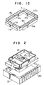
- Figs. 1A, 1B and 1C show an embodiment of the present invention, in which Fig. 1A is a perspective view, 1B an exploded perspective view, and 1C an exploded perspective view of a piezoelectric displacement unit.
- a rectangular thin metal strip 7 which is arranged in a rectangular form has vertically attached on the respective sides thereof tabular piezoelectric elements 8a, 8b; 9a, 9b; 10a, 10b; 11a, 11b with a polarization axis along the thickness directions and inner and outer electrodes.
- the tabular piezoelectric elements are so attached that the polarization axes thereof are arranged in the same direction, thereby constituting laminated piezoelectric bending of bimorph elements 8, 9, 10, 11 independent of each other.
- the central parts of the laminated piezoelectric bimorphs 10, 11 are fixedly supported by bonding or screwing with recessed fixing members 13a, 13b mountable to a base board 12, while the central parts of the piezoelectric bimorphs 8, 9 have mounted thereon a carriage 15 for carrying a movable member such as a solid-state image sensor 14.
- a carriage 15 for carrying a movable member such as a solid-state image sensor 14.
- voltage application terminals 16, 17, 18, 19 are provided, and the thin metal strip 7 is used as a common voltage application terminal 20.
- the laminated piezoelectric bimorphs 8, 9 function as both ends-supported bending elements and are displaced along the normal direction of the electrode surfaces.
- the amount of this displacement is proportional to the applied electric field and piezoelectric constant d31.
- the laminated piezoelectric elements 8a, 8b, 9a, 9b have the same thickness, and the polarization axes of the opposed laminated piezoelectric bimorphs 8, 9 are arranged in the same direction.
- the laminated piezoelectric bimorphs 8, 9 are displaced in the same amount in the same direction, so that it is possible to displace the carriage mounted at the central parts thereof along the direction of displacement of the laminated piezoelectric bimorphs 8, 9, that is, along the normal direction of the electrode surfaces.
- a voltage is applied to the terminals 20, 18, 19 in such a manner as to cause a displacement of the same amount in the same direction
- the laminated piezoelectric bimorphs 8, 9 are displaced in the same direction, that is, along the normal direction against the electrode surfaces of the piezoelectric vibrators 10, 11, thus displacing the carriage 15 in the same direction.
- the carriage 15 is displaceable in two directions on the same surface.
- the laminated piezoelectric bimorphs 8, 9, 10, 11 are constructed in the same plane, a compact micro-displacement unit capable of independent two-dimensional displacement simple in construction is provided. If conduction is assured with a grounding terminal between the voltage application terminals 16, 17, 18, 19 of the inner and outer electrodes of the laminated piezoelectric bimorphs and the fixing members, on the other hand, the resulting fact is that the thin metal strip 7 provides a common voltage application terminal 20, which reduces intrusion of noises while at the same time shorting by external contact is prevented.
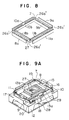
- FIG. 2 shows an example of such a package.
- a solid-state image sensor 14 is fixed on a carriage 15 of a two-dimensional micro-displacement unit by conductive adhesive or the like, and the displacement unit is fixedly mounted within a case 21 of ceramics or the like.
- the assembly is sealed in the case 21 with glass transparent to the light radiated on the light-receiving surface of the solid-state image sensor 14.
- the electric wiring to the piezoelectric elements required for two dimensional displacement and the solid-state image sensor are led out through electrodes 20 printed on the case 21.
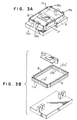
- Fig. 3A is a perspective view and Fig. 3B an exploded perspective view.
- the inner and outer electrodes 10a', 10b'; 11a', 11b' of the piezoelectric bimorphs 10, 11 fixedly supported by fixing members at the central parts thereof are isolated at the central parts as shown by hatching in Fig. 3B.
- the cantilever beam mode bimorphs on the sides of the fixed parts are driven independently.
- the laminated piezoelectric elements have the same thickness, and the opposed laminated piezoelectric bimorphs 10, 11 have the same direction of polarization axis.
- the laminated piezoelectric bimorph 8 is displaced, while by applying a voltage of the same phase to the voltage application terminals 20 and 18b, 19b in a similar manner, the laminated piezoelectric bimorph 9 is displaceable. Specifically, the laminated piezoelectric bimorphs 8 and 9 are displaced independently of each other.
- the amount of displacement of the laminated piezoelectric bimorphs 8, 9 are differentiated thereby to incline the carriage 15 in the horizontal plane.
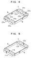
- Fig. 4 is an exploded perspective view of laminated piezoelectric bimorphs according to still another embodiment of the present invention.
- Piezoelectric bimorphs with the central parts thereof fixedly supported by fixing members are constructed of tabular piezoelectric elements 21a, 21b; 22a, 22b; 23a, 23b; 24a, 24b applied vertically on the surfaces of the thin metal strip 7 in such a manner as to be separated at the central parts thereof.
- the piezoelectric bimorphs on the sides on the fixing members are drivable independently, thereby resulting in the great advantage that an inclination can be corrected or micro positioning is made possible as described above.
- Fig. 5 is an exploded perspective view of a laminated piezoelectric bimorphs according to a further embodiment of the present invention.
- a rectangular thin metal strip 7 is formed by bending a metal sheet, and is configured in such a manner that the ends of the thin metal strip 7 are located at the central parts of the piezoelectric elements 10a, 10b to be laminated.
- the amount of displacement as a piezoelectric bimorph is not affected, and also the fact that the rectangular thin metal strip can be obtained from a sheet of metal simplifies the construction easy to fabricate.
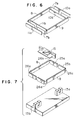
- Fig. 6 is an exploded perspective view of a laminated piezoelectric unit according to a still further embodiment of the present invention.
- Rectangular thin metal strips 7a, 7b bent in channel shape or C-shape are opposed to each other thereby to make up a thin metal strip arrangement formed in rectangle with the ends of the strips 7a, 7b at the central parts of the piezoelectric elements 10a, 10b; 11a, 11b to be laminated.
- the thin metal strips 7a, 7b are fabricated by being bent only in one direction, thereby leading to a high mass production efficiency.
- Fig. 7 is an exploded view of a micro-displacement unit according to another embodiment of the present invention.
- Micro-displacement units 25a, 25b with tabular piezoelectric elements attached vertically on the surfaces of rectangular thin metal strips 7a, 7b are bent in channel shape and arranged with the ends thereof opposed to each other.
- the ends of the micro-displacement units 25a, 25b are fixedly supported by fixing members 13a, 13b. Since this apparatus is constructed of fully independent micro displacement units, the great advantage results that the variations in the characteristics of the piezoelectric cantilever beam mode bimorphs are offset by adjusting the length of the fixed parts of the piezoelectric bimorphs at the time of mounting thereof by the fixing members.
- Fig. 8 is an exploded perspective view of a piezoelectric micro-displacement unit according to still another embodiment of the present invention.
- a piezoelectric cantilever beam mode bimorph is coupled with a laminated both ends-supported bimorph thereof by a metal thin plate, they are affected by each other.
- the modulus of flexural rigidity of the thin metal strips on the sides of the laminated piezoelectric both ends-supported bimorph thereof supported is increased by forming U-shaped recesses 26a, 26b, 26c, 26d as shown in Fig. 7 or narrow parts 26a', 26b', 26c', 26d' as shown in Fig. 8.
- apertures 27 are formed in the thin metal strip, piezoelectric elements are bonded to each other at these parts thereby to improve the bonding strength between the metal and piezoelectric elements.
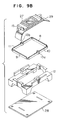
- Figs. 9A and 9B are diagrams showing a micro-displacement unit for a solid-state image sensor according to another embodiment of the present invention.
- Fig. 9A is a perspective view of the apparatus, and Fig. 9B an exploded perspective view thereof.
- a solid-state image sensor device 27 is mounted on a carriage 15. Signals of the solid-state image sensor device 27 and signals applied to voltage application terminals 16, 17, 18, 19 of laminated piezoelectric bimorphs 8, 9, 10, 11 are connected to a flexible base board 29 for connection to a printed board 28 mounted on the bottom of the base board 12.
- This construction provides an apparatus capable of accurate adjustment of mounting positions and color matching for a given solid-state image sensor device.
- a compact micro-displacement unit which is simple in construction and capable of independent displacement in two directions, comprising laminated piezoelectric bimorphs of cantilever type and laminated piezoelectric bimorphs with the ends thereof supported, both vibrators being configured in the same plane.
Description
- This invention relates to a two-dimensional piezoelectric micro-displacement unit for accurate positioning in the desired direction on the same surface. This apparatus may find applications for positioning of a color solid-state image sensor for the video camera, a displacer for high-resolution solid-state image sensor, a precision pattern positioning device and the like.
- In conventional methods of positioning by micro displacement in the order of microns or submicrons, mechanical means such as a stepping motor or a DC servo motor has been used for converting rotational motion into linear motion by a ball-type screw. The conventional mechanical apparatus has necessarily some errors due to mechanical connections and is therefore apt to be large in size in order to improve the precision thereof.
- Then, a micro displacer using the reverse piezoelectric effect of a piezoelectric element capable of electrical control has been suggested. Such a displacer has a looper-type carriage mechanism as disclosed in the Japanese Patent Publication No. 12497/76. Fig. 10 is a diagram for explaining such a looper-type carriage
mechanism having clamps 2, 3 operated by use of electrostatic or electromagnetic force at the ends of a cylindrical piezoelectric element 1. In Fig. 10(a), theclamps 2, 3 are clamped on a fixing table 4, and the clamp 3 is set free in Fig. 10(b). In Fig. 10(c), a voltage is applied to the piezoelectric element 1 to extend the same. In Fig. 10(d), the extended clamp 3 is clamped on the fixing table 4, and theclamp 2 is set free in Fig. 10(e). In Fig. 10(f), the applied voltage is removed, and in Fig. 10(g), theclamp 2 is clamped again. In this way, the same condition as in Fig. 10(a) is achieved, thus obtaining a displacement of Δℓ. A bilateral micro displacer is easily produced by mounting a similar carriage mechanism in two directions. The distortion caused by the reverse piezoelectric effect is so small that a highly accurate positioning is possible. - The Japanese Patent Laid-Open Publication No. 130677/83 and 196773/83, on the other hand, disclose a displacer for solid-state image sensor comprising a bending mode vibrator (bi-morph vibrator) with an end or both ends thereof fixed including a strip of piezoelectric elements attached on the upper and lower surfaces of a similarly-shaped thin metal plate, the piezoelectric element having a polarization axis along the thickness thereof, thus displacing the solid-state image sensor to increase the light-receiving area for a higher resolution. Fig. 11 shows a unilateral micro displacer using an example of such a bending mode vibrator. Bending
mode vibrators 5, 5' with the ends thereof fixed are arranged in parallel to each other, and acarriage 6 having a solid-state image sensor or the like thereon is disposed at the central position of thebending mode vibrators 5, 5' where the amount of displacement is maximum. - A bilateral micro displacer is easily conceivable by mounting the above-mentioned looper-type micro displacer in two directions on the same surface. In view of the fact that one of the drive units is required to be clamped by electrostatic or electromagnetic force, however, an apparatus which is portable or used by being inclined is complicated in construction requiring separate means for fixing movable members while not in operation, resulting in a bulky apparatus. Also, the weight of movable objects while moving are concentrated at the part of the apparatus unclamped thereby to make the apparatus unstable. Further, the direction of motion is determined solely by the manner in which the apparatus is mounted, but the motion in the desired direction is impossible once the apparatus is mounted.
- In a micro displacer using a bending mode vibrator, in spite of a large displacement allowable, the force generated is so weak that a heavy item cannot be moved. Also, under a heavy load, the resonant frequency of the vibrator is reduced, and the apparatus is rendered more liable to resonate to harmonic frequencies component of the drive frequency, thereby posing the problem of reduced durability. To obviate this problem by making micro displacement in the desired direction possible, a displacer (first displacement unit) with the bending mode vibrator described above may be used to displace another displacer (second displacement unit). Since the weight of the second displacement unit is exerted on the first displacement unit, however, the effect of the weight of the second displacement unit is required to be reduced by enlarging the bending mode vibrator of the first displacement unit, thereby leading to a bulky apparatus on the one hand and posing the problem of shorter durability on the other.
- From the US-A-4 520 570 is known a piezoelectric X-Y-positioner including two pairs of bimorphs located in opposition to one another, of which the bimorphs of the first pair are attached with their longitudinal centers by supports to a rigid frame. A second pair of bimorphs located in opposition to one another support at their longitudinal centers a carriage for attachement of a sample to be positioned in the X-Y-plane. The bimorphs of the second pair are connected to the bimorphs of the first pair by connectors having a square-shaped sectional area so that each two ends of a bimorph of the first and second pair are arranged orthogonally to one another such that, for a displacement in the X and Y directions, each of the bimorphs has to be bent in a double S-form, the lengthwise central part of each bimorph being in a plane parallel to the plane of the ends of the bimorphs. For bending the bimorphs into the double S-shape, each bimorph carries four independent electrodes on either side of which the electrodes at the ends are connected to voltages inverse to the voltages of the electrodes near the center of the bimorphs, which makes necessary a circuitry for the supplying voltages. Further, the two pairs of bimorphs are arranged in different planes with respect to the direction parallel to the width of the bimorphs.
- Further, from J. APPL. PHYS., vol. 59, no. 10, 15th May 1986, pages 3318-3327, American Institute of Physics; are known piezoelectric bimorphs consisting of two thin sheets of piezoceramic material one of which expands, the other contracts upon application of a voltage, such that the bending amplitude is larger than that of a unstructured bimorph material. The bimorphs described in this document also are bended into a S-shape by splitting the electrodes.
- It is an object of the present invention to provide a two-dimensional piezoelectric micro-displacement unit which has a large scanning range, is simple in construction and has compact dimensions.
- According to the present invention there is provided a two-dimensional piezoelectric micro-displacement unit comprising a plurality of piezoelectric bimorphs each including two tabular piezoelectric elements laminated to each other, said tabular piezoelectric elements having a polarization axis along the thickness direction thereof and the polarization axes of each two piezoelectric elements laminated to each other being parallel, and electrodes at the opposed surfaces thereof, a plurality of fixing members for fixedly supporting a pair of opposed located piezoelectric bimorphs at the central parts of the length thereof, and a carriage mounted on another pair of opposed located piezoelectric bimorph members, the bimorphs being connected at their lengthwise ends so that the other pair of bimorphs is supported by the one pair of bimorphs, wherein the tabular piezoelectric elements are laminated to each other on the opposing sides of a thin metal strip bent into a rectangular shape, the bent portions of the metal strip forming the connections of the bimorphs at the lengthwise ends thereof, and the pairs of piezoelectric bimorphs being configured in the same plane with respect to the rectangular shape formed by the thin metal strip.
- As a result, a compact micro displacer with simplified construction is provided which is capable of independent micro displacements in two directions.
-
- Figs. 1A, 1B, and 1C show a two-dimensional micro-displacement unit according to an embodiment of the present invention respectively, in which:
- Fig. 1A is a perspective view, 1B an exploded perspective view, and 1C an exploded perspective view of the inventive micro-displacement unit.
- Fig. 2 is an exploded perspective view of a two-dimensional micro-displacement unit in packaged form according to the present invention.
- Figs. 3A and 3B, Fig. 4, Fig. 5, Fig. 6 and Fig. 7 show other embodiments of the present invention, in which Fig. 3A is a perspective view, Fig. 3B an exploded perspective view, Fig. 4, Fig. 5 and Fig. 6 exploded perspective views of a laminated piezoelectric bimorph element, and Fig. 7 an exploded perspective view of a micro-displacement unit.
- Fig. 8 is an exploded perspective view of a laminated piezoelectric bimorph element.
- Fig. 9A is a perspective view of a micro-displacement unit for a solid-state image sensor, and Fig. 9B an exploded perspective view thereof.
- Fig. 10 and Fig. 11 are front view and perspective view of conventional micro-displacement units.
- Embodiments of the present invention will be explained in detail below with reference to the accompanying drawings.
- Figs. 1A, 1B and 1C show an embodiment of the present invention, in which Fig. 1A is a perspective view, 1B an exploded perspective view, and 1C an exploded perspective view of a piezoelectric displacement unit. A rectangular
thin metal strip 7 which is arranged in a rectangular form has vertically attached on the respective sides thereof tabularpiezoelectric elements bimorph elements piezoelectric bimorphs 10, 11 are fixedly supported by bonding or screwing withrecessed fixing members base board 12, while the central parts of thepiezoelectric bimorphs carriage 15 for carrying a movable member such as a solid-state image sensor 14. In order to assure conduction between the inner and outer electrodes of the laminatedpiezoelectric bimorphs voltage application terminals thin metal strip 7 is used as a commonvoltage application terminal 20. Upon application of a voltage to thevoltage application terminals piezoelectric bimorphs piezoelectric elements piezoelectric bimorphs laminated piezoelectric bimorphs laminated piezoelectric bimorphs laminated piezoelectric bimorphs 10, 11, with the lengthwise central parts thereof fixedly supported by the fixingmembers terminals laminated piezoelectric bimorphs piezoelectric vibrators 10, 11, thus displacing thecarriage 15 in the same direction. In view of the fact that thelaminated piezoelectric bimorphs carriage 15 is displaceable in two directions on the same surface. Also, since thelaminated piezoelectric bimorphs voltage application terminals thin metal strip 7 provides a commonvoltage application terminal 20, which reduces intrusion of noises while at the same time shorting by external contact is prevented. - The advantage of a reduced size leads to a great feature when the displacement unit is packaged with semiconductors in such applications as micro-displacement unit for a solid-state image sensor. Fig. 2 shows an example of such a package. A solid-
state image sensor 14 is fixed on acarriage 15 of a two-dimensional micro-displacement unit by conductive adhesive or the like, and the displacement unit is fixedly mounted within acase 21 of ceramics or the like. The assembly is sealed in thecase 21 with glass transparent to the light radiated on the light-receiving surface of the solid-state image sensor 14. The electric wiring to the piezoelectric elements required for two dimensional displacement and the solid-state image sensor are led out throughelectrodes 20 printed on thecase 21. - Now, another embodiment of the present invention will be described with reference to Figs. 3A and 3B. Fig. 3A is a perspective view and Fig. 3B an exploded perspective view. The inner and
outer electrodes 10a', 10b'; 11a', 11b' of thepiezoelectric bimorphs 10, 11 fixedly supported by fixing members at the central parts thereof are isolated at the central parts as shown by hatching in Fig. 3B. By applying a voltage between the such providedelectrodes voltage application terminal 20, the cantilever beam mode bimorphs on the sides of the fixed parts are driven independently. Assume, for instance, that the laminated piezoelectric elements have the same thickness, and the opposed laminatedpiezoelectric bimorphs 10, 11 have the same direction of polarization axis. When a voltage of the same phase is applied to thevoltage application terminals laminated piezoelectric bimorph 8 is displaced, while by applying a voltage of the same phase to thevoltage application terminals laminated piezoelectric bimorph 9 is displaceable. Specifically, thelaminated piezoelectric bimorphs voltage application terminals laminated piezoelectric bimorphs carriage 15 in the horizontal plane. This leads to the feature that any inclination of the solid-state image sensor mounted on the base within the horizontal plane is correctable and the angle adjustable in such applications as precision micro positioning in mask matching of integrated circuits or the like. - Fig. 4 is an exploded perspective view of laminated piezoelectric bimorphs according to still another embodiment of the present invention. Piezoelectric bimorphs with the central parts thereof fixedly supported by fixing members are constructed of tabular
piezoelectric elements 21a, 21b; 22a, 22b; 23a, 23b; 24a, 24b applied vertically on the surfaces of thethin metal strip 7 in such a manner as to be separated at the central parts thereof. In this construction, the piezoelectric bimorphs on the sides on the fixing members are drivable independently, thereby resulting in the great advantage that an inclination can be corrected or micro positioning is made possible as described above. - Fig. 5 is an exploded perspective view of a laminated piezoelectric bimorphs according to a further embodiment of the present invention. A rectangular
thin metal strip 7 is formed by bending a metal sheet, and is configured in such a manner that the ends of thethin metal strip 7 are located at the central parts of thepiezoelectric elements 10a, 10b to be laminated. In view of the fact that the ends of the thin metal strip are positioned at the parts fixed by the fixing members, the amount of displacement as a piezoelectric bimorph is not affected, and also the fact that the rectangular thin metal strip can be obtained from a sheet of metal simplifies the construction easy to fabricate. - Fig. 6 is an exploded perspective view of a laminated piezoelectric unit according to a still further embodiment of the present invention. Rectangular
thin metal strips strips piezoelectric elements 10a, 10b; 11a, 11b to be laminated. Thethin metal strips - Fig. 7 is an exploded view of a micro-displacement unit according to another embodiment of the present invention.
Micro-displacement units thin metal strips micro-displacement units members - Fig. 8 is an exploded perspective view of a piezoelectric micro-displacement unit according to still another embodiment of the present invention. In view of the fact that a piezoelectric cantilever beam mode bimorph is coupled with a laminated both ends-supported bimorph thereof by a metal thin plate, they are affected by each other. Neverthless, the modulus of flexural rigidity of the thin metal strips on the sides of the laminated piezoelectric both ends-supported bimorph thereof supported is increased by forming
U-shaped recesses narrow parts 26a', 26b', 26c', 26d' as shown in Fig. 8. In this way, the reliability is improved with a reduced mutual effect. Further, ifapertures 27 are formed in the thin metal strip, piezoelectric elements are bonded to each other at these parts thereby to improve the bonding strength between the metal and piezoelectric elements. - Figs. 9A and 9B are diagrams showing a micro-displacement unit for a solid-state image sensor according to another embodiment of the present invention. Fig. 9A is a perspective view of the apparatus, and Fig. 9B an exploded perspective view thereof. A solid-state
image sensor device 27 is mounted on acarriage 15. Signals of the solid-stateimage sensor device 27 and signals applied tovoltage application terminals piezoelectric bimorphs flexible base board 29 for connection to a printedboard 28 mounted on the bottom of thebase board 12. This construction provides an apparatus capable of accurate adjustment of mounting positions and color matching for a given solid-state image sensor device. - It will thus be understood from the foregoing description that according to the present invention, there is provided a compact micro-displacement unit which is simple in construction and capable of independent displacement in two directions, comprising laminated piezoelectric bimorphs of cantilever type and laminated piezoelectric bimorphs with the ends thereof supported, both vibrators being configured in the same plane.
Claims (11)
- A two-dimensional piezoelectric micro-displacement unit comprising a plurality of piezoelectric bimorphs (8,9, 10,11) each including two tabular piezoelectric elements (8a,8b;9a,9b;10a,10b;11a,11b) laminated to each other, said tabular piezoelectric elements (8a,8b;9a,9b;10a,10b;11a, 11b) having a polarization axis along the thickness direction thereof and the polarization axes of each two piezoelectric elements laminated to each other being parallel, and inner and outer electrodes (16,17,18,19) at the opposed surfaces thereof, a plurality of fixing members (13a,13b) for fixedly supporting a pair of opposed located piezoelectric bimorphs (10,11) at the central parts of the length thereof, and a carriage (15) mounted on another pair of opposed located piezoelectric bimorph members (8,9), the bimorphs (8,9,10,11) being connected at their lengthwise ends so that the other pair of bimorphs (8,9) is supported by the one pair of bimorphs (10,11), characterized in that the tabular piezoelectric elements (8a,8b;9a,9b;10a,10b; 11a,11b) are laminated to each other on the opposing sides of a thin metal strip (7) bent into a rectangular shape, the bent portions of the metal strip (7) forming the connections of the bimorphs at the lengthwise ends thereof, and the pairs of piezoelectric bimorphs (8,9;10,11) being configured in the same plane with respect to the rectangular shape formed by the thin metal strip (7).
- A two-dimensional piezoelectric micro-displacement unit according to claim 1, wherein the inner and outer electrodes (16,17,18,19) of said laminated piezoelectric bimorphs provide independent voltage application terminals (16,17,18,19), and said thin metal strip (7) provides a common voltage application terminal (20) for all the laminated piezoelectric bimorphs.
- A two-dimensional piezoelectric micro-displacement unit according to claim 1 or 2, wherein the inner and outer electrodes of the laminated piezoelectric bimorphs (10,11) fixedly supported by fixing members (13a,13b) are isolated at the central parts thereof for independent voltage application.
- A two-dimensional piezoelectric micro-displacement unit according to anyone of claims 1 to 3, wherein the tabular piezoelectric elements (10a,10b;11a,11b) of the pair of the piezoelectric bimorphs (10,11) fixedly supported at the central parts thereof by fixing members (13a,13b) are isolated at the fixed parts thereof.
- A two-dimensional piezoelectric micro-displacement unit according to anyone of claims 1 to 4, wherein the ends of said thin metal strip (7) are coincident with the fixed central parts of the laminated piezoelectric bimorphs (10, 11) fixedly supported by the fixing members (13a,13b).
- A two-dimensional piezoelectric micro-displacement unit according to anyone of claim 1 to 4, wherein two C-shaped strips of thin metal (7a,7b) are formed into a rectangular form, the ends of said two thin metal strips (7a,7b) being coincident with the central fixed parts of the laminated piezoelectric bimorphs (8,9) fixedly supported by fixing members (13a,13b).
- A two-dimensional piezoelectric micro-displacement unit according to anyone of claims 1 to 4, comprising two micro displacement arrangements (25a,25b) each including tabular piezoelectric elements attached to the inner and outer surfaces of a thin strip of metal bent into a C-shape, said micro displacement arrangements (25a,25b) being arranged with the ends thereof opposed to each other, said ends being fixedly supported by fixing members (13a,13b).
- A two-dimensional piezoelectric micro-displacement unit according to anyone of claims 1 to 7, wherein a plurality of apertures (27) are formed into the thin strip of metal.
- A two-dimensional piezoelectric micro-displacement unit according to anyone of claims 1 to 8, wherein the modulus of flexural rigidity of the thin metal strip (7) at the ends of the laminated piezoelectric vibrators (8,9) having the carriage (15) mounted thereon is increased by an U-shaped form (26a-26d) or narrow parts (26a'-26d').
- A two-dimensional piezoelectric micro-displacement unit according to anyone of claims 1 to 9, wherein the carriage (15) has mounted thereon a solid-state image sensor (14).
- A two-dimensional piezoelectric micro-displacement unit according to claim 10, comprising a flexible base board (12) wherein signals of the solid-state image sensor (14) mounted on the carriage (15) are processed externally and the voltage application signals applied to the laminated piezoelectric bimorphs (8,9,10,11) are produced externally.
Applications Claiming Priority (4)
| Application Number | Priority Date | Filing Date | Title |
|---|---|---|---|
| JP61165848A JPH0691635B2 (en) | 1986-07-15 | 1986-07-15 | Micro displacement device |
| JP165848/86 | 1986-07-15 | ||
| JP49296/87 | 1987-03-04 | ||
| JP62049296A JPH0671321B2 (en) | 1987-03-04 | 1987-03-04 | Micro displacement device for solid-state image sensor |
Publications (3)
| Publication Number | Publication Date |
|---|---|
| EP0253375A2 EP0253375A2 (en) | 1988-01-20 |
| EP0253375A3 EP0253375A3 (en) | 1989-12-06 |
| EP0253375B1 true EP0253375B1 (en) | 1993-02-03 |
Family
ID=26389674
Family Applications (1)
| Application Number | Title | Priority Date | Filing Date |
|---|---|---|---|
| EP87110218A Expired - Lifetime EP0253375B1 (en) | 1986-07-15 | 1987-07-15 | Two-dimensional piezoelectric actuator |
Country Status (2)
| Country | Link |
|---|---|
| EP (1) | EP0253375B1 (en) |
| DE (1) | DE3783960T2 (en) |
Cited By (3)
| Publication number | Priority date | Publication date | Assignee | Title |
|---|---|---|---|---|
| WO2005104257A1 (en) * | 2004-04-23 | 2005-11-03 | Agency For Science, Technology And Research | Micro-electromechanical device |
| US7777782B2 (en) | 2005-11-04 | 2010-08-17 | Nokia Corporation | Stabilization of an image produced by optics |
| US8041201B2 (en) | 2008-04-03 | 2011-10-18 | Nokia Corporation | Camera module having movable lens |
Families Citing this family (10)
| Publication number | Priority date | Publication date | Assignee | Title |
|---|---|---|---|---|
| JPH08280185A (en) * | 1995-04-07 | 1996-10-22 | Nikon Corp | Ultrasonic actuator |
| JPH10105243A (en) | 1996-09-10 | 1998-04-24 | Hewlett Packard Co <Hp> | Positioning feature, positioning device and information recorder |
| US6252333B1 (en) | 1998-02-20 | 2001-06-26 | Seiko Instruments Inc. | Stage utilizing ultrasonic motor and electronic equipment and printer utilizing the stage |
| US6017313A (en) | 1998-03-20 | 2000-01-25 | Hypertension Diagnostics, Inc. | Apparatus and method for blood pressure pulse waveform contour analysis |
| DE19927129C1 (en) | 1999-06-15 | 2001-01-04 | Wolf Gmbh Richard | Focusing and focal width adjuster for video camera with zoom lens produces time window which is supplied to focusing circuit and zoom control circuit to provide vertical scanning gap of video signal |
| US6331161B1 (en) * | 1999-09-10 | 2001-12-18 | Hypertension Diagnostics, Inc | Method and apparatus for fabricating a pressure-wave sensor with a leveling support element |
| GB0203897D0 (en) * | 2002-02-19 | 2002-04-03 | Pbt Ip Ltd | Low cost actuator with 2 dimensional motion |
| US7214919B2 (en) * | 2005-02-08 | 2007-05-08 | Micron Technology, Inc. | Microelectronic imaging units and methods of manufacturing microelectronic imaging units |
| EP1969417A4 (en) * | 2005-11-30 | 2010-03-24 | Nokia Corp | Method and system for image stabilization |
| US10516348B2 (en) | 2015-11-05 | 2019-12-24 | Mems Drive Inc. | MEMS actuator package architecture |
Family Cites Families (1)
| Publication number | Priority date | Publication date | Assignee | Title |
|---|---|---|---|---|
| US4520570A (en) * | 1983-12-30 | 1985-06-04 | International Business Machines Corporation | Piezoelectric x-y-positioner |
-
1987
- 1987-07-15 EP EP87110218A patent/EP0253375B1/en not_active Expired - Lifetime
- 1987-07-15 DE DE8787110218T patent/DE3783960T2/en not_active Expired - Fee Related
Cited By (4)
| Publication number | Priority date | Publication date | Assignee | Title |
|---|---|---|---|---|
| WO2005104257A1 (en) * | 2004-04-23 | 2005-11-03 | Agency For Science, Technology And Research | Micro-electromechanical device |
| US7596841B2 (en) | 2004-04-23 | 2009-10-06 | Agency For Science Technology And Research | Micro-electromechanical devices and methods of fabricating thereof |
| US7777782B2 (en) | 2005-11-04 | 2010-08-17 | Nokia Corporation | Stabilization of an image produced by optics |
| US8041201B2 (en) | 2008-04-03 | 2011-10-18 | Nokia Corporation | Camera module having movable lens |
Also Published As
| Publication number | Publication date |
|---|---|
| DE3783960D1 (en) | 1993-03-18 |
| EP0253375A3 (en) | 1989-12-06 |
| DE3783960T2 (en) | 1993-05-27 |
| EP0253375A2 (en) | 1988-01-20 |
Similar Documents
| Publication | Publication Date | Title |
|---|---|---|
| EP0253375B1 (en) | Two-dimensional piezoelectric actuator | |
| EP0149017B1 (en) | Piezoelectric x-y positioner | |
| US5543956A (en) | Torsional vibrators and light deflectors using the torsional vibrator | |
| US7109639B2 (en) | Vibration-type driving device, control apparatus for controlling the driving of the vibration-type driving device, and electronic equipment having the vibration-type driving device and the control apparatus | |
| JP2839543B2 (en) | Displacement generator | |
| CN101284642B (en) | Micromechanical device with tilted electrodes | |
| US7649301B2 (en) | Actuator capable of driving with large rotational angle or large deflection angle | |
| JP4511120B2 (en) | Ultrasonic linear motor | |
| US7508114B2 (en) | Ultrasonic motor | |
| US20060061235A1 (en) | Ultrasonic motor and method for operating the same | |
| KR20220055488A (en) | Camera module and mobile terminal | |
| JPH01251965A (en) | Solid-state image pickup device | |
| JPS62152379A (en) | Bidirectional microdisplacement device | |
| JP3348777B2 (en) | Differential piezoelectric actuator | |
| CN111077628A (en) | Piezoelectric lens driving device, camera device, and electronic apparatus | |
| JPH0646207A (en) | Piezoelectric drive micro scanner | |
| EP3974890A1 (en) | Microelectromechanical device having a structure tiltable by piezoelectric actuation about two rotation axes | |
| JP2009044861A (en) | Driving device | |
| JPS62152380A (en) | Bidirectional microdisplacement device | |
| JPH0691635B2 (en) | Micro displacement device | |
| KR20080093882A (en) | Driving device | |
| JP3605899B2 (en) | Optical scanner device | |
| JPH0455355B2 (en) | ||
| JPS62107685A (en) | Bidirectional fine displacing device | |
| JPH0671321B2 (en) | Micro displacement device for solid-state image sensor |
Legal Events
| Date | Code | Title | Description |
|---|---|---|---|
| PUAI | Public reference made under article 153(3) epc to a published international application that has entered the european phase |
Free format text: ORIGINAL CODE: 0009012 |
|
| AK | Designated contracting states |
Kind code of ref document: A2 Designated state(s): DE FR GB |
|
| RIN1 | Information on inventor provided before grant (corrected) |
Inventor name: YAMASHITA, ICHIRO Inventor name: WAKAMIYA, MASAYUKI Inventor name: FUKADA, TETSUJI |
|
| PUAL | Search report despatched |
Free format text: ORIGINAL CODE: 0009013 |
|
| AK | Designated contracting states |
Kind code of ref document: A3 Designated state(s): DE FR GB |
|
| 17P | Request for examination filed |
Effective date: 19900110 |
|
| 17Q | First examination report despatched |
Effective date: 19910902 |
|
| GRAA | (expected) grant |
Free format text: ORIGINAL CODE: 0009210 |
|
| AK | Designated contracting states |
Kind code of ref document: B1 Designated state(s): DE FR GB |
|
| REF | Corresponds to: |
Ref document number: 3783960 Country of ref document: DE Date of ref document: 19930318 |
|
| ET | Fr: translation filed | ||
| PLBE | No opposition filed within time limit |
Free format text: ORIGINAL CODE: 0009261 |
|
| STAA | Information on the status of an ep patent application or granted ep patent |
Free format text: STATUS: NO OPPOSITION FILED WITHIN TIME LIMIT |
|
| 26N | No opposition filed | ||
| REG | Reference to a national code |
Ref country code: GB Ref legal event code: 746 Effective date: 19960628 |
|
| PGFP | Annual fee paid to national office [announced via postgrant information from national office to epo] |
Ref country code: FR Payment date: 19990709 Year of fee payment: 13 |
|
| PGFP | Annual fee paid to national office [announced via postgrant information from national office to epo] |
Ref country code: GB Payment date: 19990714 Year of fee payment: 13 |
|
| PGFP | Annual fee paid to national office [announced via postgrant information from national office to epo] |
Ref country code: DE Payment date: 19990716 Year of fee payment: 13 |
|
| PG25 | Lapsed in a contracting state [announced via postgrant information from national office to epo] |
Ref country code: GB Free format text: LAPSE BECAUSE OF NON-PAYMENT OF DUE FEES Effective date: 20000715 |
|
| GBPC | Gb: european patent ceased through non-payment of renewal fee |
Effective date: 20000715 |
|
| PG25 | Lapsed in a contracting state [announced via postgrant information from national office to epo] |
Ref country code: FR Free format text: LAPSE BECAUSE OF NON-PAYMENT OF DUE FEES Effective date: 20010330 |
|
| REG | Reference to a national code |
Ref country code: FR Ref legal event code: ST |
|
| PG25 | Lapsed in a contracting state [announced via postgrant information from national office to epo] |
Ref country code: DE Free format text: LAPSE BECAUSE OF NON-PAYMENT OF DUE FEES Effective date: 20010501 |