EP0196839A2 - Piezoelectric transducer and components therefor - Google Patents
Piezoelectric transducer and components therefor Download PDFInfo
- Publication number
- EP0196839A2 EP0196839A2 EP86302108A EP86302108A EP0196839A2 EP 0196839 A2 EP0196839 A2 EP 0196839A2 EP 86302108 A EP86302108 A EP 86302108A EP 86302108 A EP86302108 A EP 86302108A EP 0196839 A2 EP0196839 A2 EP 0196839A2
- Authority
- EP
- European Patent Office
- Prior art keywords
- piezoelectric
- layer
- conductive
- piezoelectric transducer
- conductive layer
- Prior art date
- Legal status (The legal status is an assumption and is not a legal conclusion. Google has not performed a legal analysis and makes no representation as to the accuracy of the status listed.)
- Ceased
Links
- 239000000463 material Substances 0.000 claims abstract description 14
- 239000002033 PVDF binder Substances 0.000 claims description 13
- 229920002981 polyvinylidene fluoride Polymers 0.000 claims description 13
- 239000004033 plastic Substances 0.000 claims description 4
- 229920003023 plastic Polymers 0.000 claims description 4
- 239000004020 conductor Substances 0.000 claims description 3
- 229920001577 copolymer Polymers 0.000 claims description 3
- MIZLGWKEZAPEFJ-UHFFFAOYSA-N 1,1,2-trifluoroethene Chemical compound FC=C(F)F MIZLGWKEZAPEFJ-UHFFFAOYSA-N 0.000 claims description 2
- BQCIDUSAKPWEOX-UHFFFAOYSA-N 1,1-Difluoroethene Chemical compound FC(F)=C BQCIDUSAKPWEOX-UHFFFAOYSA-N 0.000 claims description 2
- 239000010410 layer Substances 0.000 description 40
- 239000010408 film Substances 0.000 description 11
- PXHVJJICTQNCMI-UHFFFAOYSA-N Nickel Chemical compound [Ni] PXHVJJICTQNCMI-UHFFFAOYSA-N 0.000 description 9
- 229920005989 resin Polymers 0.000 description 8
- 239000011347 resin Substances 0.000 description 8
- 239000003822 epoxy resin Substances 0.000 description 6
- 239000008187 granular material Substances 0.000 description 6
- 229920000647 polyepoxide Polymers 0.000 description 6
- 238000010276 construction Methods 0.000 description 4
- 229920000134 Metallised film Polymers 0.000 description 3
- 238000000151 deposition Methods 0.000 description 3
- 230000000694 effects Effects 0.000 description 3
- 239000002184 metal Substances 0.000 description 3
- 229910052751 metal Inorganic materials 0.000 description 3
- 239000011104 metalized film Substances 0.000 description 3
- 238000002604 ultrasonography Methods 0.000 description 3
- 239000004593 Epoxy Substances 0.000 description 2
- 241000206607 Porphyra umbilicalis Species 0.000 description 2
- 239000000919 ceramic Substances 0.000 description 2
- 230000008021 deposition Effects 0.000 description 2
- 239000000945 filler Substances 0.000 description 2
- 239000000203 mixture Substances 0.000 description 2
- 229910052759 nickel Inorganic materials 0.000 description 2
- 239000011236 particulate material Substances 0.000 description 2
- 229910000679 solder Inorganic materials 0.000 description 2
- 229920003319 Araldite® Polymers 0.000 description 1
- -1 BiO Substances 0.000 description 1
- 239000012790 adhesive layer Substances 0.000 description 1
- 229910000416 bismuth oxide Inorganic materials 0.000 description 1
- 229910010293 ceramic material Inorganic materials 0.000 description 1
- 238000005520 cutting process Methods 0.000 description 1
- 230000007423 decrease Effects 0.000 description 1
- 230000003247 decreasing effect Effects 0.000 description 1
- 230000001627 detrimental effect Effects 0.000 description 1
- 238000003745 diagnosis Methods 0.000 description 1
- TYIXMATWDRGMPF-UHFFFAOYSA-N dibismuth;oxygen(2-) Chemical compound [O-2].[O-2].[O-2].[Bi+3].[Bi+3] TYIXMATWDRGMPF-UHFFFAOYSA-N 0.000 description 1
- 238000009826 distribution Methods 0.000 description 1
- 230000005684 electric field Effects 0.000 description 1
- 239000012777 electrically insulating material Substances 0.000 description 1
- 238000005530 etching Methods 0.000 description 1
- PCHJSUWPFVWCPO-UHFFFAOYSA-N gold Chemical compound [Au] PCHJSUWPFVWCPO-UHFFFAOYSA-N 0.000 description 1
- 239000010931 gold Substances 0.000 description 1
- 229910052737 gold Inorganic materials 0.000 description 1
- 238000004519 manufacturing process Methods 0.000 description 1
- 238000009659 non-destructive testing Methods 0.000 description 1
- 239000002245 particle Substances 0.000 description 1
- 230000002093 peripheral effect Effects 0.000 description 1
- 230000000704 physical effect Effects 0.000 description 1
- 239000004848 polyfunctional curative Substances 0.000 description 1
- 239000011342 resin composition Substances 0.000 description 1
- 229920003002 synthetic resin Polymers 0.000 description 1
- 239000000057 synthetic resin Substances 0.000 description 1
- 239000010409 thin film Substances 0.000 description 1
Images

Classifications
-
- H—ELECTRICITY
- H01—ELECTRIC ELEMENTS
- H01L—SEMICONDUCTOR DEVICES NOT COVERED BY CLASS H10
- H01L29/00—Semiconductor devices adapted for rectifying, amplifying, oscillating or switching, or capacitors or resistors with at least one potential-jump barrier or surface barrier, e.g. PN junction depletion layer or carrier concentration layer; Details of semiconductor bodies or of electrodes thereof ; Multistep manufacturing processes therefor
- H01L29/02—Semiconductor bodies ; Multistep manufacturing processes therefor
- H01L29/06—Semiconductor bodies ; Multistep manufacturing processes therefor characterised by their shape; characterised by the shapes, relative sizes, or dispositions of the semiconductor regions ; characterised by the concentration or distribution of impurities within semiconductor regions
- H01L29/08—Semiconductor bodies ; Multistep manufacturing processes therefor characterised by their shape; characterised by the shapes, relative sizes, or dispositions of the semiconductor regions ; characterised by the concentration or distribution of impurities within semiconductor regions with semiconductor regions connected to an electrode carrying current to be rectified, amplified or switched and such electrode being part of a semiconductor device which comprises three or more electrodes
-
- H—ELECTRICITY
- H10—SEMICONDUCTOR DEVICES; ELECTRIC SOLID-STATE DEVICES NOT OTHERWISE PROVIDED FOR
- H10N—ELECTRIC SOLID-STATE DEVICES NOT OTHERWISE PROVIDED FOR
- H10N30/00—Piezoelectric or electrostrictive devices
- H10N30/01—Manufacture or treatment
- H10N30/06—Forming electrodes or interconnections, e.g. leads or terminals
-
- H—ELECTRICITY
- H10—SEMICONDUCTOR DEVICES; ELECTRIC SOLID-STATE DEVICES NOT OTHERWISE PROVIDED FOR
- H10N—ELECTRIC SOLID-STATE DEVICES NOT OTHERWISE PROVIDED FOR
- H10N30/00—Piezoelectric or electrostrictive devices
- H10N30/30—Piezoelectric or electrostrictive devices with mechanical input and electrical output, e.g. functioning as generators or sensors
- H10N30/308—Membrane type
Definitions
- This invention relates to piezoelectric transducers and their construction.
- Piezoelectric transducers commonly employ a ceramic piezoelectric element having electrodes on its oppositely polarised surfaces.
- a change of stress in the piezoelectric element produces a temporary potential difference across the electrodes, and conversely a change in potential difference across the electrodes induces a temporary change in stress within the element.
- plastics material especially polyvinylidene fluoride (PVdF).
- PVdF polyvinylidene fluoride
- the piezoelectric layer is polarised across the thickness of the laver, and electrodes are formed by depositinq conductive lavers, for example of metallised film, on opposite surfaces of the piezoelectric layer. Where an area of electrode on one surface lies directly opposite an area of electrode on the opposite surface (in the specification we will use the term "overlaps") there is produced the active piezoelectric transducer region of the device.
- the electrode areas can be readily shaped, for example by selective deposition of metallised film, or by selectively etching away portions of a deposited film.
- piezoelectric transducers with specifically desired properties can be produced, especially for example for use as ultrasonic transducers capable of transmitting a focussed or shaped ultrasound signal.
- An additional advantage of using selective deposition of metallised film is that when an electric field is applied to pole the film or cause it to become electro- active, it is possible to restrict the activity to defined areas.
- the wanted signal is produced in and transmitted from the active piezoelectric region, and portions of an electrode which project beyond the region (i.e. do not overlap part of an opposite electrode) do not produce any appreciable piezoelectric signal, and are therefore often provided for attaching electrical conductors to the electrodes. Without these non-active regions of the electrode used for making electrical contact, undesirable signals can be generated and provide an unwanted background "noise" which interferes with the signal produced or detected by the piezoelectric active region.
- the present invention provides an improved design of piezoelectric transducer component and transducers incorporatinq such components.
- a piezoelectric transducer component comprising a layer of piezoelectric material having conductive electrode layers applied to opposite surfaces thereof, the conductive layers having overlapping areas defining an active piezoelectric region between them, and non-overlapping areas to which electrical connections are made, characterised in that one of the conductive layers is larger in area than the opposite conductive layer and has a window in it in register with a portion of the opposite conductive layer to which portion an electrical connection is made.
- an electrical connection is made with the larger conductive layer through an opening in the piezoelectric layer in a said non-overlapping area of the larger conductive layer.
- the piezoelectric component may comprise a plurality of transducer elements produced by a number of said smaller conductive layers spaced apart over an area covered by a larger conductive layer on the opposite surface of the piezoelectric layer.
- the piezoelectric layer is preferably a plastics material; most preferably PVdF or a copolymer of vinylidene fluoride/trifluoroethylene (VdF/TrFE).
- a piezoelectric transducer comprising a casing having an opening in one face, a piezoelectric component as described above extending across the opening with the larger conductive layer on the outside and the smaller conductive layer or layers together with the electrical connections on the inside; the casing preferably being made of a conductive material and electrically connected to the external larger conductive layer of the transducer component.
- the transducer component comprises a PVdF film 10 which has been treated in known manner to make it piezoelectric.
- a conductive layer 12 for example of gold, suitably applied by known vapour deposition techniques.
- the conductive layer 12 takes the form of a disc, and has a small rectangular extension 14 to one side.
- the other surface of the layer 10 is completely coated with a metallised layer 16, except for a generally rectangular window 18 which is coincident with the extension 14 on the other surface, but slightly (about 0.5 mm) larger on the sides remote from the disc 12, thereby creating a narrow gap 20 where there is no metallised layer on either surface.
- the piezoelectrically active region defined between two overlapping metallised areas, is the region defined by the disc 12, since all other parts of the film 16 have a conductive layer on one side only or on neither side.
- An electrical connection is made to the metallised layer 12 in conventional manner by adhering an electrical lead 22 to the extension region 14 using for example conductive epoxy resin 24 or solder.
- An electrical connection is made with the other metallised surface 16 by making a hole 28 through the film outside the active region, passing an electrical lead 26 through the hole and adhering it to the conductive layer 16 by conductive epoxy resin 30 or solder.
- the electrical leads 22,26 extend in the same direction from the surface of the film 10 which carries a smaller conductive area 12,14.
- a casing 40 is made from metal, and is provided at one end with for example an externally screw- threaded boss 42 for connection to a suitable support, and at the opposite end with an opening 44, in this case circular and of the same size as the disc 12.
- the film 10 is cut to an appropriate size around the inactive region outside the disc 10 so that it will fit inside the casing 40 over the opening 44 so as to be supported peripherally by the casing around the opening.
- this peripheral region 45 around the opening can suitably be made of synthetic resin such as epoxy material.
- the transducer component is peripherally secured in place with the larger conductive surface 16 facinq outwardly of the casinq and the smaller conductive disc 12 on the inside of the casing in register with the opening 44.
- the electrical leads 22,26 also lie inside the casing.
- the lead from the external conductive surface 16 is connected to the metal casing 40, while the lead 22 from the conductive disc 12 is taken to a terminal 46 in the boss 42 insulated from the casing 40; the interior of the casing being then filled with an electrically insulating material 48 such as an epoxy resin.
- a preferred material 48 is a filled resin, wherein the filler comprises bismuth oxide or PVdF granules, preferably both, and most preferably also nickel powder.
- the filler comprises bismuth oxide or PVdF granules, preferably both, and most preferably also nickel powder.
- 100 parts by weight of Araldite (Ciba-Geigy trade mark) CY1301 epoxy resin, 30 parts HY1300 hardener, 180 parts BiO and 60 parts Ni are mixed and poured into the transducer casing through the top 42.
- PVdF granules typically 1.5 x 3 mm, are then added to the resin in the casing so as to form a virtually continuous layer at the top (remote from the piezoelectric element) with the density of qranule concentration decreasing downwards so that there are virtually no granules close to the piezoelectric element.
- the resin is then allowed to harden.
- the resulting transducer has a number of significant properties arising from the nature of the backing material 48. To begin with, there is no separate bonding material between the piezoelectric element and the backing, as there is with conventional piezoelectric devices, and this eliminates one source of unwanted signal. Then, the PVdF granules reduce the signal loss due to reflection from the top face of the resin, while the Ni and BiO particles scatter the reflected signals, while at the same time provide sufficient density to the resin to orevent the PVdF q ranules from sinking to the bottom (near the piezoelectric element).
- Granules other than PVdF could be used, but it is convenient to use the same material as that used to make the piezoelectric layer, and PVdF has suitable properties for reducing stray reflected signals.
- the graded distribution of the qranules through the depth of the epoxy resin is useful in randomizing the reflections of the unwanted signals.
- Nickel is convenient as a filler for scattering the unwanted reflections and increasing the density of the resin composition. However, too much nickel would make the resin conductive, and since there is no insulating adhesive layer between the resin backing and the piezoelectric element, this would be obviously detrimental.
- BiO is insulating and dense, and provides likewise good acoustic properties for scattering the unwanted signal.
- BiO, Ni and resin are not critical, and can generally be varied within about 10% of the figures given above without significant effect in performance.
- All three materials, BiO, Ni and PVdF granules have a high acoustic mismatch with epoxy resin, which aids the acoustic scattering effect and minimises unwanted signals from the back of the transducer.
- the particulate materials can be used separately or in combinations of two of them, but optimum performance is obtained by the use of all three particulate materials.
- the extension 14 of the inner conductive layer 12 there is only one region from which substantial background noise might be produced; namely the extension 14 of the inner conductive layer 12, and this is closely surrounded by the outer conductive surface 16 which is connected to the casing and acts as a screen, thereby limiting the amount of electrical noise emission from the area 14.
- the area 14 may be about 2 to 3 mm square.
- the transducer can be used for example to emit an ultrasound signal and pick up any returning echo. Such devices are useful in ultrasound scanners in medical diagnosis, and in non-destructive testing of materials.
- the present invention is particularly suitable for the production of multi-element transducer components, examples of which are shown in Figs 4 to 6.
- a single piezoelectric film 10 is provided with a single conductive layer 16 on one side and a series of smaller conductive layers 12 on the other side.
- Each conductive layer 12 has an extension 14 lying over a window 18 in the conductive layer 16, and has a respective lead 22 connected to the extension 14.
- a single electrical connection 26 can be made to the conductive layer 16.
- the construction of Fig. 4 may be used to produce individual separate transducer components by cutting the sheet between the elements, in which case separate connections 26 will have to be provided for each element.
- the active regions in the embodiment shown in Fig. 4 are shown as being rectangular, but they could be any desired shape or mixture of shapes.
- Fig. 5 shows an embodiment in which the smaller conductive surfaces are provided on one side of the piezoelectric film 10 in the form of a central disc 12A (or it could be a ring) surrounded by a series of concentric ings 12B,C,D...etc..
- Each conductive surface 12 is provided with a respective electrical connector 22A to 22D etc. from respective extension elements lying over respective windows in the single conductive layer 16 provided on the other surface of the film 10.
- the conductive areas 12A to 12D etc. are designed so as to have the same area, and thus their width decreases as their diameter increases.
- the device as shown in Fig. 5 can be incorporated in a transducer illustrated in Fig. 6, of analogous construction to that shown in Fig. 7, except of course that the electrical leads 22A to 22D will be taken to separate terminals insulated from the casing 40. Also, the windows 18 will obviously extend radially over the surface 16, and if desired these can be covered by an extension limb 50 of the epoxy rim 45 of the casinq.
Abstract
Description
- This invention relates to piezoelectric transducers and their construction.
- Piezoelectric transducers commonly employ a ceramic piezoelectric element having electrodes on its oppositely polarised surfaces. A change of stress in the piezoelectric element produces a temporary potential difference across the electrodes, and conversely a change in potential difference across the electrodes induces a temporary change in stress within the element. More recently it has been discovered that a piezoelectric element can be made from plastics material, especially polyvinylidene fluoride (PVdF). This has different piezoelectric characteristics from ceramic elements, and has useful physical properties which make it easier and cheaper to fashion piezoelectric devices, especially high frequency devices, for example because the plastics material can easily be prepared as a thin film, whereas it is very difficult to prepare and handle a correspondingly thin layer of ceramic material.
- In a thin layer piezoelectric device, the piezoelectric layer is polarised across the thickness of the laver, and electrodes are formed by depositinq conductive lavers, for example of metallised film, on opposite surfaces of the piezoelectric layer. Where an area of electrode on one surface lies directly opposite an area of electrode on the opposite surface (in the specification we will use the term "overlaps") there is produced the active piezoelectric transducer region of the device. The electrode areas can be readily shaped, for example by selective deposition of metallised film, or by selectively etching away portions of a deposited film. In this way piezoelectric transducers with specifically desired properties can be produced, especially for example for use as ultrasonic transducers capable of transmitting a focussed or shaped ultrasound signal. An additional advantage of using selective deposition of metallised film is that when an electric field is applied to pole the film or cause it to become electro- active, it is possible to restrict the activity to defined areas.
- The wanted signal is produced in and transmitted from the active piezoelectric region, and portions of an electrode which project beyond the region (i.e. do not overlap part of an opposite electrode) do not produce any appreciable piezoelectric signal, and are therefore often provided for attaching electrical conductors to the electrodes. Without these non-active regions of the electrode used for making electrical contact, undesirable signals can be generated and provide an unwanted background "noise" which interferes with the signal produced or detected by the piezoelectric active region.
- If these non-active connector regions are bent out of the olane of the piezoelectric layer, it has been found that they are very liable to fail in a relatively short time, and so the life of the device is reduced.
- The present invention provides an improved design of piezoelectric transducer component and transducers incorporatinq such components.
- Accordinq to one aspect of the present invention there is provided a piezoelectric transducer component comprising a layer of piezoelectric material having conductive electrode layers applied to opposite surfaces thereof, the conductive layers having overlapping areas defining an active piezoelectric region between them, and non-overlapping areas to which electrical connections are made, characterised in that one of the conductive layers is larger in area than the opposite conductive layer and has a window in it in register with a portion of the opposite conductive layer to which portion an electrical connection is made. Preferably, an electrical connection is made with the larger conductive layer through an opening in the piezoelectric layer in a said non-overlapping area of the larger conductive layer. The piezoelectric component may comprise a plurality of transducer elements produced by a number of said smaller conductive layers spaced apart over an area covered by a larger conductive layer on the opposite surface of the piezoelectric layer. The piezoelectric layer is preferably a plastics material; most preferably PVdF or a copolymer of vinylidene fluoride/trifluoroethylene (VdF/TrFE).
- In another aspect of the present invention there is provided a piezoelectric transducer comprising a casing having an opening in one face, a piezoelectric component as described above extending across the opening with the larger conductive layer on the outside and the smaller conductive layer or layers together with the electrical connections on the inside; the casing preferably being made of a conductive material and electrically connected to the external larger conductive layer of the transducer component.
- In order that the invention may be more clearly understood, various embodiments will now be described with reference to the accompanying drawings, wherein:
- Fig. 1 shows a view on one surface of a transducer component,
- Fig. 2 shows a view on the opposite surface of the transducer component, and
- Fig. 3 shows a cross-section through the component along the line III-III of Fig. 1, with the thickness of the layers greatly exaggerated for clarity;
- Fig. 4 shows a perspective view of another embodiment of piezoelectric component,
- Fig. 5 shows a perspective view of a third embodiment of piezoelectric comoonent,
- Fiq. 6 shows a oerspective view of a transducer incorporating the component of Fig. 5, and
- Fig. 7 shows a cross-sectional side view through a transducer incorporating for example a piezoelectric component of Figs 1 to 3.
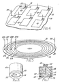
- Referring to the drawings and firstly to Figs 1 to 3; the transducer component comprises a
PVdF film 10 which has been treated in known manner to make it piezoelectric. On one surface of the film is applied aconductive layer 12, for example of gold, suitably applied by known vapour deposition techniques. Theconductive layer 12 takes the form of a disc, and has a smallrectangular extension 14 to one side. - As shown in Fig. 2, the other surface of the
layer 10 is completely coated with ametallised layer 16, except for a generallyrectangular window 18 which is coincident with theextension 14 on the other surface, but slightly (about 0.5 mm) larger on the sides remote from thedisc 12, thereby creating anarrow gap 20 where there is no metallised layer on either surface. Thus, the piezoelectrically active region, defined between two overlapping metallised areas, is the region defined by thedisc 12, since all other parts of thefilm 16 have a conductive layer on one side only or on neither side. - An electrical connection is made to the
metallised layer 12 in conventional manner by adhering anelectrical lead 22 to theextension region 14 using for exampleconductive epoxy resin 24 or solder. An electrical connection is made with the othermetallised surface 16 by making ahole 28 through the film outside the active region, passing anelectrical lead 26 through the hole and adhering it to theconductive layer 16 byconductive epoxy resin 30 or solder. Thus, theelectrical leads film 10 which carries a smallerconductive area - The manner in which such a transducer can be used is illustrated in Fig. 7. A
casing 40 is made from metal, and is provided at one end with for example an externally screw- threadedboss 42 for connection to a suitable support, and at the opposite end with an opening 44, in this case circular and of the same size as thedisc 12. Thefilm 10 is cut to an appropriate size around the inactive region outside thedisc 10 so that it will fit inside thecasing 40 over the opening 44 so as to be supported peripherally by the casing around the opening. Whereas the casing as a whole is made of metal, thisperipheral region 45 around the opening can suitably be made of synthetic resin such as epoxy material. The transducer component is peripherally secured in place with the largerconductive surface 16 facinq outwardly of the casinq and the smallerconductive disc 12 on the inside of the casing in register with the opening 44. Thus, the electrical leads 22,26 also lie inside the casing. The lead from the externalconductive surface 16 is connected to themetal casing 40, while thelead 22 from theconductive disc 12 is taken to aterminal 46 in theboss 42 insulated from thecasing 40; the interior of the casing being then filled with an electrically insulatingmaterial 48 such as an epoxy resin. - A
preferred material 48 is a filled resin, wherein the filler comprises bismuth oxide or PVdF granules, preferably both, and most preferably also nickel powder. In a typical composition, 100 parts by weight of Araldite (Ciba-Geigy trade mark) CY1301 epoxy resin, 30 parts HY1300 hardener, 180 parts BiO and 60 parts Ni are mixed and poured into the transducer casing through thetop 42. PVdF granules, typically 1.5 x 3 mm, are then added to the resin in the casing so as to form a virtually continuous layer at the top (remote from the piezoelectric element) with the density of qranule concentration decreasing downwards so that there are virtually no granules close to the piezoelectric element. The resin is then allowed to harden. - The resulting transducer has a number of significant properties arising from the nature of the
backing material 48. To begin with, there is no separate bonding material between the piezoelectric element and the backing, as there is with conventional piezoelectric devices, and this eliminates one source of unwanted signal. Then, the PVdF granules reduce the signal loss due to reflection from the top face of the resin, while the Ni and BiO particles scatter the reflected signals, while at the same time provide sufficient density to the resin to orevent the PVdF qranules from sinking to the bottom (near the piezoelectric element). - Granules other than PVdF could be used, but it is convenient to use the same material as that used to make the piezoelectric layer, and PVdF has suitable properties for reducing stray reflected signals. The graded distribution of the qranules through the depth of the epoxy resin is useful in randomizing the reflections of the unwanted signals.
- Nickel is convenient as a filler for scattering the unwanted reflections and increasing the density of the resin composition. However, too much nickel would make the resin conductive, and since there is no insulating adhesive layer between the resin backing and the piezoelectric element, this would be obviously detrimental. BiO is insulating and dense, and provides likewise good acoustic properties for scattering the unwanted signal.
- The amounts and relative proportions of BiO, Ni and resin are not critical, and can generally be varied within about 10% of the figures given above without significant effect in performance.
- All three materials, BiO, Ni and PVdF granules have a high acoustic mismatch with epoxy resin, which aids the acoustic scattering effect and minimises unwanted signals from the back of the transducer. The particulate materials can be used separately or in combinations of two of them, but optimum performance is obtained by the use of all three particulate materials.
- In the construction shown in Fig. 6, there is only one region from which substantial background noise might be produced; namely the
extension 14 of the innerconductive layer 12, and this is closely surrounded by the outerconductive surface 16 which is connected to the casing and acts as a screen, thereby limiting the amount of electrical noise emission from thearea 14. Typically thearea 14 may be about 2 to 3 mm square. - The transducer can be used for example to emit an ultrasound signal and pick up any returning echo. Such devices are useful in ultrasound scanners in medical diagnosis, and in non-destructive testing of materials.
- Many variations are possible on the size, shape and configuration of the piezoelectrically active region, and the type of transducer device into which the piezoelectric element is incorporated. The present invention is particularly suitable for the production of multi-element transducer components, examples of which are shown in Figs 4 to 6.
- In Fig. 4, a single
piezoelectric film 10 is provided with a singleconductive layer 16 on one side and a series of smallerconductive layers 12 on the other side. Eachconductive layer 12 has anextension 14 lying over awindow 18 in theconductive layer 16, and has arespective lead 22 connected to theextension 14. Thus, an array of transducer elements is provided, and if they are intended to be used in that form, then a singleelectrical connection 26 can be made to theconductive layer 16. However, the construction of Fig. 4 may be used to produce individual separate transducer components by cutting the sheet between the elements, in which caseseparate connections 26 will have to be provided for each element. The active regions in the embodiment shown in Fig. 4 are shown as being rectangular, but they could be any desired shape or mixture of shapes. - Fig. 5 shows an embodiment in which the smaller conductive surfaces are provided on one side of the
piezoelectric film 10 in the form of acentral disc 12A (or it could be a ring) surrounded by a series ofconcentric ings 12B,C,D...etc.. Eachconductive surface 12 is provided with a respectiveelectrical connector 22A to 22D etc. from respective extension elements lying over respective windows in the singleconductive layer 16 provided on the other surface of thefilm 10. Theconductive areas 12A to 12D etc. are designed so as to have the same area, and thus their width decreases as their diameter increases. - The device as shown in Fig. 5 can be incorporated in a transducer illustrated in Fig. 6, of analogous construction to that shown in Fig. 7, except of course that the
electrical leads 22A to 22D will be taken to separate terminals insulated from thecasing 40. Also, thewindows 18 will obviously extend radially over thesurface 16, and if desired these can be covered by anextension limb 50 of theepoxy rim 45 of the casinq.
Claims (11)
Applications Claiming Priority (2)
| Application Number | Priority Date | Filing Date | Title |
|---|---|---|---|
| GB8507596 | 1985-03-23 | ||
| GB858507596A GB8507596D0 (en) | 1985-03-23 | 1985-03-23 | Piezoelectric transducer |
Publications (2)
| Publication Number | Publication Date |
|---|---|
| EP0196839A2 true EP0196839A2 (en) | 1986-10-08 |
| EP0196839A3 EP0196839A3 (en) | 1988-09-28 |
Family
ID=10576518
Family Applications (1)
| Application Number | Title | Priority Date | Filing Date |
|---|---|---|---|
| EP86302108A Ceased EP0196839A3 (en) | 1985-03-23 | 1986-03-21 | Piezoelectric transducer and components therefor |
Country Status (2)
| Country | Link |
|---|---|
| EP (1) | EP0196839A3 (en) |
| GB (2) | GB8507596D0 (en) |
Cited By (11)
| Publication number | Priority date | Publication date | Assignee | Title |
|---|---|---|---|---|
| EP0451533A1 (en) * | 1990-03-16 | 1991-10-16 | Hoechst CeramTec Aktiengesellschaft | Piezoelectric ceramic transducer disc and process for making the same |
| EP0796669A2 (en) * | 1996-03-19 | 1997-09-24 | Siemens Aktiengesellschaft | Ultrasonic transducer |
| WO2001059852A2 (en) * | 2000-02-09 | 2001-08-16 | Sri International | Monolithic electroactive polymers |
| WO2008052541A1 (en) * | 2006-11-03 | 2008-05-08 | Danfoss A/S | A capacitive transducer with cutting areas |
| US9195058B2 (en) | 2011-03-22 | 2015-11-24 | Parker-Hannifin Corporation | Electroactive polymer actuator lenticular system |
| US9231186B2 (en) | 2009-04-11 | 2016-01-05 | Parker-Hannifin Corporation | Electro-switchable polymer film assembly and use thereof |
| US9425383B2 (en) | 2007-06-29 | 2016-08-23 | Parker-Hannifin Corporation | Method of manufacturing electroactive polymer transducers for sensory feedback applications |
| US9553254B2 (en) | 2011-03-01 | 2017-01-24 | Parker-Hannifin Corporation | Automated manufacturing processes for producing deformable polymer devices and films |
| US9590193B2 (en) | 2012-10-24 | 2017-03-07 | Parker-Hannifin Corporation | Polymer diode |
| US9761790B2 (en) | 2012-06-18 | 2017-09-12 | Parker-Hannifin Corporation | Stretch frame for stretching process |
| US9876160B2 (en) | 2012-03-21 | 2018-01-23 | Parker-Hannifin Corporation | Roll-to-roll manufacturing processes for producing self-healing electroactive polymer devices |
Citations (3)
| Publication number | Priority date | Publication date | Assignee | Title |
|---|---|---|---|---|
| US3872332A (en) * | 1971-04-19 | 1975-03-18 | Honeywell Inc | Composite bond for acoustic transducers |
| FR2389238A1 (en) * | 1977-04-25 | 1978-11-24 | Rosenthal Technik Ag | Very flat piezoelectric push button switch - has flat laminate comprising metal or plastics foil on piezoelectric wafer |
| US4417170A (en) * | 1981-11-23 | 1983-11-22 | Imperial Clevite Inc. | Flexible circuit interconnect for piezoelectric element |
Family Cites Families (3)
| Publication number | Priority date | Publication date | Assignee | Title |
|---|---|---|---|---|
| GB1536066A (en) * | 1976-01-29 | 1978-12-20 | Seiko Instr & Electronics | Piezo-electric vibrator |
| JPS6318175Y2 (en) * | 1980-11-10 | 1988-05-23 | ||
| EP0059447B1 (en) * | 1981-02-28 | 1985-05-15 | Kinseki, Ltd. | Piezoelectric oscillator device |
-
1985
- 1985-03-23 GB GB858507596A patent/GB8507596D0/en active Pending
-
1986
- 1986-03-21 GB GB08607092A patent/GB2173637B/en not_active Expired
- 1986-03-21 EP EP86302108A patent/EP0196839A3/en not_active Ceased
Patent Citations (3)
| Publication number | Priority date | Publication date | Assignee | Title |
|---|---|---|---|---|
| US3872332A (en) * | 1971-04-19 | 1975-03-18 | Honeywell Inc | Composite bond for acoustic transducers |
| FR2389238A1 (en) * | 1977-04-25 | 1978-11-24 | Rosenthal Technik Ag | Very flat piezoelectric push button switch - has flat laminate comprising metal or plastics foil on piezoelectric wafer |
| US4417170A (en) * | 1981-11-23 | 1983-11-22 | Imperial Clevite Inc. | Flexible circuit interconnect for piezoelectric element |
Cited By (14)
| Publication number | Priority date | Publication date | Assignee | Title |
|---|---|---|---|---|
| EP0451533A1 (en) * | 1990-03-16 | 1991-10-16 | Hoechst CeramTec Aktiengesellschaft | Piezoelectric ceramic transducer disc and process for making the same |
| EP0796669A2 (en) * | 1996-03-19 | 1997-09-24 | Siemens Aktiengesellschaft | Ultrasonic transducer |
| EP0796669A3 (en) * | 1996-03-19 | 1998-04-29 | Siemens Aktiengesellschaft | Ultrasonic transducer |
| WO2001059852A2 (en) * | 2000-02-09 | 2001-08-16 | Sri International | Monolithic electroactive polymers |
| WO2001059852A3 (en) * | 2000-02-09 | 2002-02-21 | Stanford Res Inst Int | Monolithic electroactive polymers |
| US6664718B2 (en) | 2000-02-09 | 2003-12-16 | Sri International | Monolithic electroactive polymers |
| WO2008052541A1 (en) * | 2006-11-03 | 2008-05-08 | Danfoss A/S | A capacitive transducer with cutting areas |
| US9425383B2 (en) | 2007-06-29 | 2016-08-23 | Parker-Hannifin Corporation | Method of manufacturing electroactive polymer transducers for sensory feedback applications |
| US9231186B2 (en) | 2009-04-11 | 2016-01-05 | Parker-Hannifin Corporation | Electro-switchable polymer film assembly and use thereof |
| US9553254B2 (en) | 2011-03-01 | 2017-01-24 | Parker-Hannifin Corporation | Automated manufacturing processes for producing deformable polymer devices and films |
| US9195058B2 (en) | 2011-03-22 | 2015-11-24 | Parker-Hannifin Corporation | Electroactive polymer actuator lenticular system |
| US9876160B2 (en) | 2012-03-21 | 2018-01-23 | Parker-Hannifin Corporation | Roll-to-roll manufacturing processes for producing self-healing electroactive polymer devices |
| US9761790B2 (en) | 2012-06-18 | 2017-09-12 | Parker-Hannifin Corporation | Stretch frame for stretching process |
| US9590193B2 (en) | 2012-10-24 | 2017-03-07 | Parker-Hannifin Corporation | Polymer diode |
Also Published As
| Publication number | Publication date |
|---|---|
| GB2173637B (en) | 1988-11-16 |
| EP0196839A3 (en) | 1988-09-28 |
| GB8507596D0 (en) | 1985-05-01 |
| GB8607092D0 (en) | 1986-04-30 |
| GB2173637A (en) | 1986-10-15 |
Similar Documents
| Publication | Publication Date | Title |
|---|---|---|
| US4728844A (en) | Piezoelectric transducer and components therefor | |
| US8319399B2 (en) | Ultrasound probe | |
| EP0397959B1 (en) | Annular array sensors | |
| EP0196839A2 (en) | Piezoelectric transducer and components therefor | |
| EP0458146B1 (en) | Ultrasonic transducer with reduced acoustic cross coupling | |
| RU2419388C2 (en) | Ultrasonic probe | |
| JPS6133516B2 (en) | ||
| US4704774A (en) | Ultrasonic transducer and method of manufacturing same | |
| US4611372A (en) | Method for manufacturing an ultrasonic transducer | |
| JPH0110079Y2 (en) | ||
| EP0265679B1 (en) | Flexural disk transducer | |
| US3510698A (en) | Electroacoustical transducer | |
| KR20190073572A (en) | Ultrasonic transducer | |
| JPS5851697A (en) | Ultrasonic wave transceiver | |
| JPH0242898A (en) | Ultrasonic oscillator | |
| JP6542769B2 (en) | Mass production of single element ultrasonic transducers | |
| JPH0833097A (en) | Piezoelectric element | |
| JPH0678398A (en) | Ultrasonic wave transducer | |
| CN217726112U (en) | Annular ultrasonic transducer | |
| JP3614075B2 (en) | Ultrasonic probe | |
| JP2601503B2 (en) | Array type ultrasonic probe | |
| JPS62133900A (en) | Acoustic attenuating material for ultrasonic sensor | |
| JPS59202059A (en) | Probe for ultrasonic tomographic apparatus | |
| JP2022086307A (en) | Ultrasonic transducer | |
| JPH0765986B2 (en) | Array type ultrasonic probe |
Legal Events
| Date | Code | Title | Description |
|---|---|---|---|
| PUAI | Public reference made under article 153(3) epc to a published international application that has entered the european phase |
Free format text: ORIGINAL CODE: 0009012 |
|
| AK | Designated contracting states |
Kind code of ref document: A2 Designated state(s): AT BE CH DE FR IT LI LU NL SE |
|
| PUAL | Search report despatched |
Free format text: ORIGINAL CODE: 0009013 |
|
| AK | Designated contracting states |
Kind code of ref document: A3 Designated state(s): AT BE CH DE FR IT LI LU NL SE |
|
| 17P | Request for examination filed |
Effective date: 19881231 |
|
| 17Q | First examination report despatched |
Effective date: 19910201 |
|
| STAA | Information on the status of an ep patent application or granted ep patent |
Free format text: STATUS: THE APPLICATION HAS BEEN REFUSED |
|
| 18R | Application refused |
Effective date: 19910817 |
|
| RIN1 | Information on inventor provided before grant (corrected) |
Inventor name: CROCKER, ROBERT Inventor name: STEWART, DUNCAN Inventor name: KENT, PETER Inventor name: WILSON, PAUL |